Embed Size (px)
Citation preview
IYOKAN - Institutional Repository : the EHIME area http://iyokan.lib.ehime-u.ac.jp/dspace/
>> 愛媛大学 - Ehime University
This document is downloaded at: 2017-10-15 14:52:59
Title PWM Amplifier and Its Application to Sinusoidal WaveInverter
Author(s) MIYAUCHI, Masayoshi
Citation 愛媛大学教育学部紀要. 第III部, 自然科学. vol.15, no.1,p.83-98
Issue Date 1994-09-30
URL http://iyokan.lib.ehime-u.ac.jp/dspace/handle/iyokan/2960
Rights
Note
Mem. Fac. Educ. Ehime Univ.,Nat. Sci., Vol. 15, No. 1 83'xJ98 (1994)
PWM to
Amplifier and Its
Sinusoida! WaveApplicationInverter
Masayoshi MiyAucHiDePartments of Technology, Faculty of Education,
Ehime University, Bunleyo-cho, Matsuyama, 790
(Received April 28, 1994)
ABSTRACT
This paper deals with both a power amplifier equipped with switched type puls-width-
modulated (PWM) operation and its application to the compound method PWM sinusoidal
wave inverters is proposed.
This PWM amplifier and inverters are clarified by means of the frequency spectrum
distributions of the og,tput PWM signals analyzed by double Fourier series expansions, and its
spectrum distributions are shown by the experimental results.
We describe that a new switching method and compound method (PWM sinusoidal wave
inverters) are available for obtaining good sinusoidal output signals and applicable to AC
power sources for the devices, such as UPS, CVCF and the use of high frequency power in-
verters.
Key words: Power electronics, PWM amplifier, PWM sinusoidal wave inverter, Fre-
quency spectrum distribution, double Fourier series expansion, switched modulation type
PWM, compound method PWM, optimum PWM method, high frequency power inverter,Uniterruptible power supply, constant voltage constant frequency power source.
1. Introduction
Since pulse-width modulation (hereafter abbreviated as PWM) is a simplified method
and yet is capable of providing high output power, various amplifiers for power circuitshave been devised, and several practicable methods have already been r6alized.(i)"V(4)
Especially, when the input signals to PWM are limited to those having sinusoidal
waveforms, it is usable as the sinusoidal waveform inverter utilizable in the recent power
83
Masayoshi MIyAucHI
electronic technology fields, and so it is applicable to AC power sources for the devices
such as UPS (uninterruptible power supply), CVCF (constant voltage constant frequency), (5) (6) (8)and so on.
In the present paper, the basic principles, the configuration methods, andcharacteristics of this PWM sinusoidal wave amplifier are presented, and particularly, due
to the excellent characteristics of a switched modulation type PWM sinusoidal waveform
amplifier, its utilization as inverter devices is described. And then a compound PWM
sinusoidal inverter, er the theoretically extended method thereof, as an inverter adopting
this optimum PWM method, are proposed; the characteristics of each method is clarified by
means of double Fourier series expansions, computer simulations, and experiments on trial
models; and their applications are described,
2. Basic configurations and operation principles of PWM amplifier
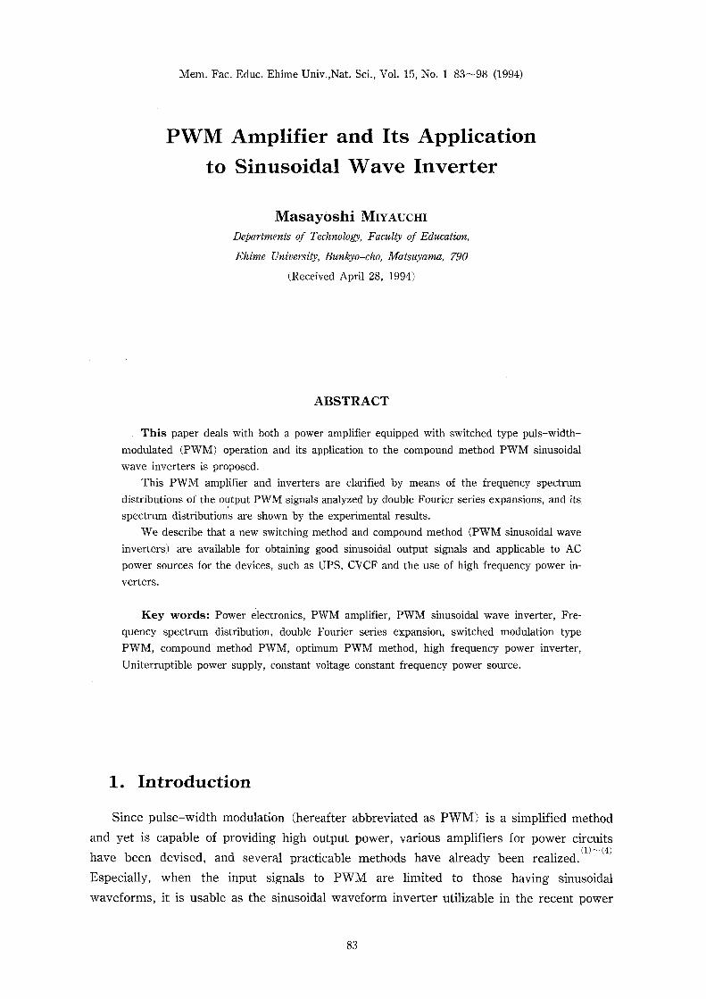
Figs. 1 and 2 show the basic configurations and the operating principles of PWM
amplifier, respectively. The amplitude of the input signal Vi(t) is compared with that of a
DC Powersource Å}Em
lnput signalVi(Q
g(el
Compara-tor
Switehelement
Output filterLPF
Output signal Ve
Specified biassignal Eo(t) PWMsignat ' Fig. 1 PWM amplifier basic configuration.
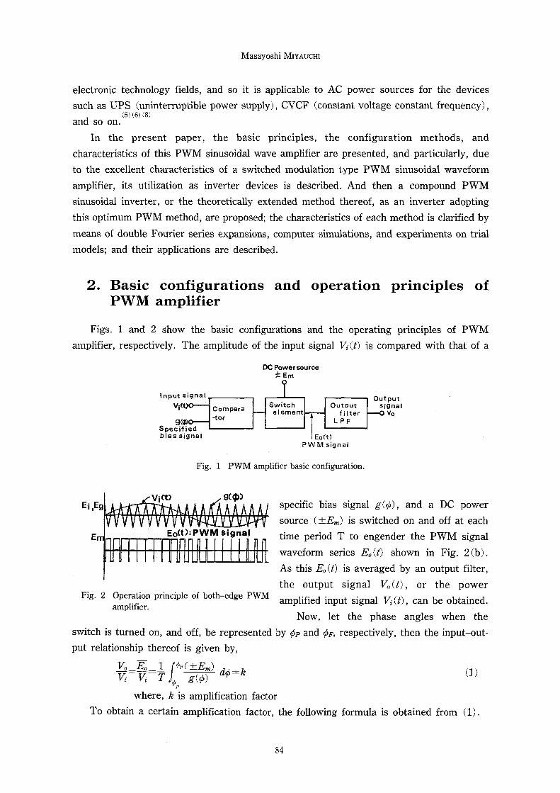
vi ro gcÅë) specific bias signal g(ip), and a DC power E•i Eg
source (Å}Em) is switched on and off at each Eo(t):PWMSignat time period T to engender the PWM signal
waveform series E,(t) shown in Fig. 2(b).
As this E,(t) is averaged by an output filter,
the output signal V,(t), or the power Fig' 2 .0mPeprl,a.ft.ie'Orn, Pri"CiPle Of bOth-edge PWM amplified input signal Vi(t), can be obtained.
Now, let the phase angles when theswitch is turned on, and off, be represented by ipp and ipF, respectively, then the input-out-
put relationship thereof is given by,
S/==tt/==i f,eF(.',k) dip-le (i) P where, le is amplification factor
To obtain a certain amplification factor, the following formula is obtained from (1).
84
PWM Amplifier and Its Application to Sinusoidal Wave Inverter
g(Åë)=Å}-TlfE-lemdÅë (2) For a specific bias signal, an integrated waveform of the power source may be adopted.
Here, the PWM signals Eo(t), when a single sinusoidal waveform (Ei sin wst) is input,
assuming that the repetition angular frequency of the specific bias signal is tu, (=2z/T),
can be expanded generally by the following double Fourier series, and the frequency spec-
trum is obtained as follows.
oo
=is known as both-edge type PWM, and the R'5 Emagnitude represents the relative values of
each harmonic wave component and thepower source voltage. In the figure, "X"
marks denote the theoretical values of each of Fig.those obtained from (4), and coincides com-
pletely with the measured values thereof.
If tus<<toc, than the input signals (ws component)
region sufficiently separated from other components
monic wave components'),
a output circuit; consequently, an amplifier having an
linear characteristics can be realized.
Now, assuming that the ratio (SN ratio) of the
necessary harmonic wave components is equal to or
imum angular frequency
that tu, is separable from cac-4ws, the following
Wsm = (oc15
A LPF,quency of cac/5, is needed for the output filter. In
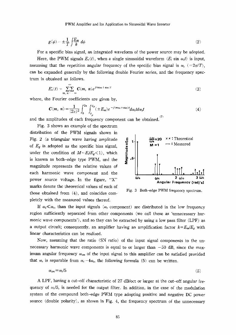
system of the compound both-edge PWM typesource (double polarity), as shown in Fig. 4, the
85
E6(t) == ZZ C(m, n)ej(mws+ndic)t
m, n=- oowhere, the Fourier coefficients are given by,
C(m, n) = (21n)2 fo2" fipOF(Å}E.)e mj'(Mcos+"toc)tdto,tdw,t
P (7)and the amplitudes of each frequency component can be obtained.
Fig. 3 shows an example of the spectrum
distribution of the PWM signals shown in
Fig. 2 (a triangular wave having amplitude .E 1 {S.\='20of Eg is adopted as the specific bias signal, :. M"1under the condition of M=EilEg<1), which .-5-
x x : Theoretical
- : Measured
(3)
(4)
Ws wc 2coc 3toc Angular Frequency Cradls]
3 Both-edge PWM frequency spectrum.
are distributed in the low frequency
(we call these as `unnecessary har-
and so they can be extracted by using a low pass filter (LPF) as
amplification factor le=EmlEg with
input signal components to the un-
larger than -50 dB, since the max- tosm of the input signal to this amplifier can be satisfied provided
formula (5) can be written.
(5)
having a cut-off characteristic of 27 dB/oct or larger at the cut-off angular fre-
addition, in the case of the modulation
adopting positive and negative DC power
frequency spectrum of the unnecessary
Masayoshi MiyAucHi
EiEg
Em
E-1:g•"=-
? .5E
-
Ka!.2ocvs
M =1
x pt i Theoretical
- l Measured
M
CVs wc 2coc 3coc Angular Frequency Crad!sJ
Fig. 4 Double-polar both-edge PWM operation and its frequency spectrum.
dynamic range and the improvement of the
which are to be achieved by the degeneracy of the unnecessary harmonic wave components
included in the PWM signals. Especially, to
the modulation method is needed.
harmonic wave components includes only 2n
w, sideband components of the both-edge
PWM (Fig. 3). Its maximum amplitudevalue diminishes, and the upper limit angular
frequency of the input sinusoidal wave
signals, capable of being amplified, is
lowered.
In such a way, for the realization of the
PWM sinusoidal wave amplifier, its inherent
characteristics are determined according to
the sorts of PWM being employed. For apreferable configuration, the following two
items are generally considered as the re-
quirements to be met, i.e., (D The realization
of the amplification mechanism intended for
the increase of the amplitude of the output
sinusoidal wave; @ The enlargement of the
accuracy of the output waveforms, both of
meet the requirements of @, contrivance in
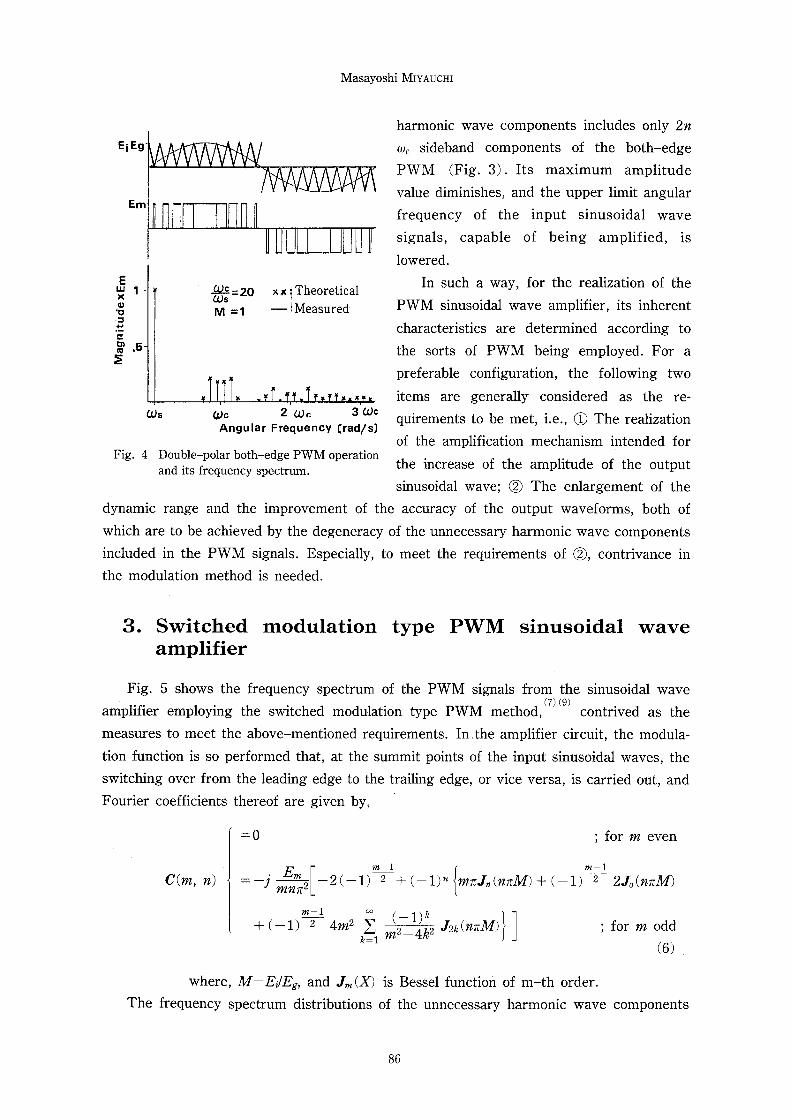
3. Switched modulation type PWM sinusoidal wave amplifier
Fig. 5 shows the frequency spectrum of the PWM signals from the sinusoidal wave (7) (9)amplifier employing the switched modulation type PWM method, contrived as the
measures to meet the above-mentioned requirements. In.the amplifier circuit, the modula-
tion function is so performed that, at the summit points of the input sinusoidal waves, the
switching over from the leading edge to the trailing edge, or vice versa, is carried out, and
Fourier coefficients thereof are given by,
=O 'formeven '
C(m, n) == -7' mEnM.2[-2(-1)M2-i+(-1)" (mzJ.(nzM) +(-1)M2-i 2J,(nzM)
+(-1)M2Mi 4m2 lei.li m(E-ltÅí2 J2le(nzM))] ;for m odd
(6)
where, M=Ei/Eg, and J.(X) is Bessel function of m-th order.
The frequency spectrum distributions of the unnecessary harmonic wave components
86
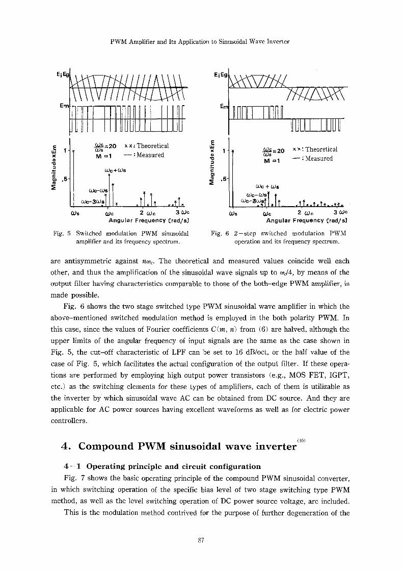
s:g==-
?E•
EiiE
1
.5
PWM Amplifier and Its Application to Sinusoidal Wave Inverter
EiEg
.SZ2g=2o xx:TheoreticalCL)$
M=1 -:Measured
(Dc+ COs
<L)C, - toS
cLke3tos
E
s:ig•-=-
Etn' •5
Ct)s M =1
cac + cos
tuc- coscvÅë-Sws
.gs2s2=2o xX:Theoretical
-- :Measured
cos cvc 2coc 3Wc cvs wc 2coc 3tuc Angular Frequency Crad!s] Angular Frequency Crad!$JFig. 5 Switched modulation PWM sinusoidal Fig. 6 2-step switched tnodulation PWM
amplifier and its frequency spectrum. operation and its frequency spectrum.
are antisymmetric against ntu,. The theoretical and measured values coincide well each
other, and thus the amplification of the sinusoidal wave signals up to toc/4, by means of the
output filter having characteristics comparable to those of the both-edge PWM amplifier, is
made possible.
Fig. 6 shows the two stage switched type PWM sinusoidal wave amplifier in which the
above-mentioned switched modulation method is employed in the both polarity PWM. In
this case, since the values of Fourier coefficients C(m, n) from (6) are halved, although the
upper limits of the angular frequency of input signals are the same as the case Shown in
Fig. 5, the cut-off characteristic of LPF can be set to 16 dBloct, or the half value of the
case of Fig. 5, which facilitates the actual configuration of the output filter. If these opera-
tions are performed by employing high output power transistors (e.g., MOS FET, IGPT,
etc.) as the switching elements for these types of amplifiers, each of thern is utilizable as
the inverter by which sinusoidal wave AC can be obtained from DC source. And they are
applicable for AC power sources having excellent waveforms as well as for electric power
controllers.
(10) 4. Compound PWM sinusoidal wave inverter
4-1 Operating principle and circuit configuration Fig. 7 shows the basic operating principle of the compound PWM sinusoidal converter,
in which switching operation of the specific bias level of two stage switching type PWM
method, as well as the level switching operation of DC power source voltage, are included.
This is the modulation method contrived for the purpose of further degeneration of the
87
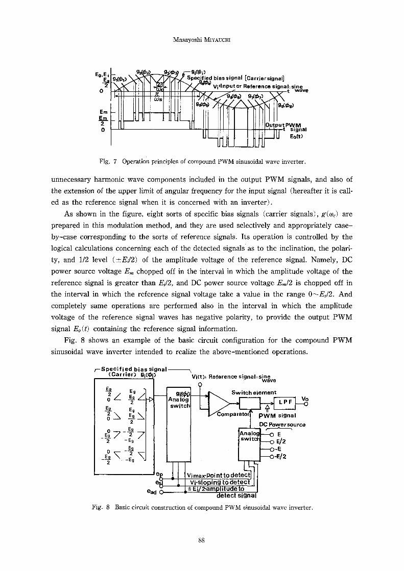
Masayoshi MIyAucHI
Eg,Ei .!Eia
2 o
Em Em 2 o
gKÅë,)
ab gstosl ir5gei(cto'ti)lÅíeuldbiassignat(carriersignaij
- vi.'lnput.orReferencesignal:sinert
casgKÅë!)
g"ÅëpgKÅë7)gafÅëal
twav
slgnaEo(t)
O.uttputtPWM
Fig. 7 Operation principles of compound PWM sinusoidal wave inverter.
unnecessary harmonic wave components included in the output PWM signals, and also of
the extension of the upper limit of angular frequency for the input signal (hereafter it is call-
ed as the reference signal when it is concerned with an inverter).
As shown in the figure, eight sorts of specific bias signals (carrier signals), g(tu,) are
prepared in this modulation method, and they are used selectively and appropriately case-
by--case corresponding to the sorts of reference signals. Its operation is controlled by the
logical calculations concerning each of the detected signals as to the inclination, the polari-
ty, and 1/2 level (Å}Ei/2) of the amplitude voltage of the reference signal. Namely, DC
power source voltage E. chopped off in the interval in which the amplitude voltage of the
reference signal is greater than Ei/2, and DC power source voltage Em/2 is chopped off in
the interval in which the reference signal voltage take a value in the range Ot-Es/2. And
completely same operations are performed also in the interval in which the amplitude
voltage of the reference signal waves has negative polarity, to provide the output PWM
signal Eo(t) containing the reference signal information.
Fig. 8 shows an example of the basic circuit configuration for the compound PWM
sinusoidal wave inverter intended to realize the above-mentioned operations.
r--Specified bias signa17 giCÅëi) Vict): Reference signat:sine CCarrier) wave
Switchelement gl top vo Analog LPF switch 21> Comparator PWM s''ignal DC Powersource
EEg.
g,< Eg,< aE E2g g i)>, s,x 2 Eg.;• 7la, 7
-EEg--!ll• Y -g, y
e
Analogswitc
Vi max• Poi nt to detect
E
agead
Vi•sloping to detectÅ}Ei• 2.amplitu eto
Fig. 8
E/2..E
-E/2
detect signal
Basic circuit construction of compound PWM sinusoidal wave inverter.
88
PWM Amplifier and Its Application to Sinusoidal Wave Inverter
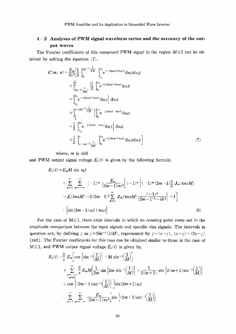
4-2 Analyses of PWM signal waveform series and the accuracy of the out-
put waves The Fourier coefficients of this compound PWM signal in the region MS1 can be ob-
tained by solving the equation (7),
c(m, n) ==Sllltff[S Sii"-i(iilii) S:ie-j(mtust+nwct)dto,tdto,t
n + Sii.-,("t) (ll I:2e-j(mwst+nevct)dto,t
+ Silerj(MWst+ntuct)dtu,t) dtu,t
+ ig-sin'i(it) (!i3e-j(mtost+nwct)dw,t
+ll S2X3e -j(mtust+nwct)dto,t] dto,t
+li !l-,i.n,(21ttT) I:`e-j(Mwst+nwct)dtu,tdto,t] (7)
where, m is oddand PWM output signal voltage E,(t) is given by the following formula.
Eo(t) =EmM sin cast
+.Eli .=200-. (-1)M (2m.EMI)m2[(-1)"((-1)m(2m-1)E Jm(4nzM)
-J,(4nnM) -2(2m-1)2lei.;, J2k(4nnan (2mg-1)12)-k 4le21 +1]
•(sin (2m-1) to,t+ntu,t] (8) For the case of M;})1, there exist intervals in which no crossing point come out in the
amplitude comparison between the input signals and specific vias signals. The intervals in
question are, by defining r as r=Sinri(11M), represented by rn--(z-r), (z+r)--(2n-r)
[rad]. The Fourier coefficients for this case can be obtained similar to those in the case of
M-<1, and PWM output signal voltage E,(t) is given by,
Eo(t) =-; Em[cos (sin-i(jl})) +Msin-i(il)F)]
+.=iSi.. ; EinM[Sitlt sin (2m sin-i(ili)) +2(ml+1) sin (2 (m+1)sin-i(ili)l
m\O +cos ( (2m+1)sinmi(jl})) ]sin (2m+1) ca,t
-.S.i ..Åí.oor. (2mEMI)m2[si" ((2m+1)sinT'(5Ii)1
89
Masayoshi MIyAucHI
- (2m-1)Jm (4nzM) sin-i(
oo-(2m-1) Z Jle(4nnM) fek=#-.Oo
• (sin(2in-1)tust+ntoct)
jl})
1
2m-1-le
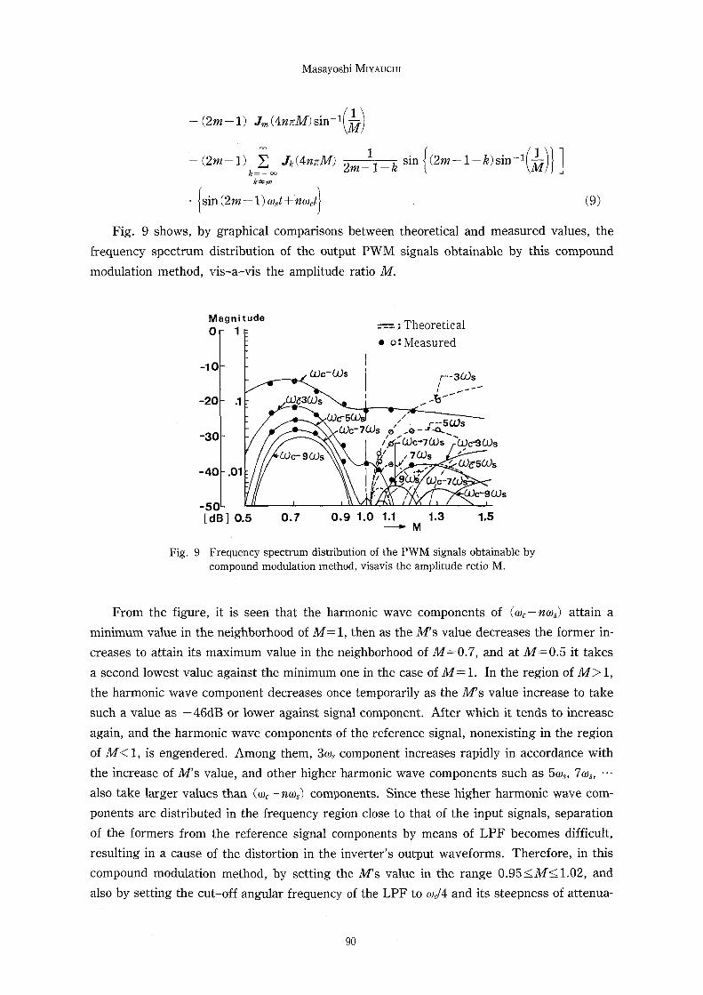
Fig. 9 shows, by graphical comparisons between
frequency spectrum distribution of the output PWM
modulation method, vis-a-vis the amplitude ratio M.
sin ( (2m -1 - le) sinmi( 1
M)1 ]
theoretical and measured
signals obtainable by this
(9)
values, the
compound
Fig.
Magnitudeo
--1 O
-20
-30
-40
-50
1
.1
.Ol
[dB]
=- ; Theoretical
e o:Measured l coc-CDs l /r--3CS'E.
CV63CDs i ..B-'t tuCco-5,C.Lls7co..i/.e-="a5coS
N. /ssi'COc-e7CDs "'cDcsCOscoc--gcos B/.e if' 7CV.s. . 7 'co' .---scv.
!lf. .gNSfl,iil,"'"cL,,c'--722}
• 'tst CL)c-9(t)s
O.5 O.7 O.9 1.0 1.1 t.3 -M
1.5
9 Frequency spectrum distribution of the PWM signals obtainable by compound modulation method, visavis the amplitude retio M.
From the figure, it is seen that the harmonic wave components of (toc-ncas) attain a
minimum value in the neighborhood of M==1, then as the M's value decreases the former in-
creases to attain its maximum value in the neighborhood of M=:O.7, and at M=O.5 it takes
a second lowest value against the minimum one in the case of M =1. In the region of M>1,
the harmonic wave component decreases once temporarily as the M"s value increase to take
such a value as -46dB or lower against signal component. After which it tends to increase
again, and the harmonic wave components of the reference signal, nonexisting in the region
of M<1, is engendered. Among them, 3ws component increases rapidly in accordance with
the increase of M's value, and other higher harmonic wave components such as 5ws, 7tos, '''
also take larger values than (w,-ntu,) components. Since these higher harmonic wave com-
ponents are distributed in the frequency region close to that of the input signals, separation
of the formers from the reference signal components by means of LPF becomes difficult,
resulting in a cause of the distortion in the inverter's output waveforms. Therefore, in this
compound modulation method, by setting the M's value in the range O.95sl;ME{1,02, and
also by setting the cut-off angular frequency of the LPF to toc/4 and its steepness of attenua-
90
PWM Amplifier and Its Application to Sinusoidal Wave Inverter
tion characteristic to 14 dB/oct, an inverter having a favorable output waveform accuracy
can be obtained. However, in this modulation method, a problem of the errors in the switch-
ed modulation at the maximum amplitude of the reference sinusoidal wave also comes out.
Now, by letting the delay angle of the switched modulation point from the summit point
of the reference sinusoidal wave signal, be Åë (rad), then the Fourier coefficients, consisting
of five sorts of components concerning the output PWM waveform series, for the region of
ME{1, are given by,
(1) DC component
C(O, O)-O (10) (2) Signal component
c(o, o)--1' E2MM (11) (3) Higher harmonic wave component of reference signal
C(m, O) -O (12) (4) Higher harmonic wave component of the specific bias signal
C(O, n) =O (13) (5) Sum and difference components between the higher harmonic wave of specific bias
signal and the signal's higher harmonic wave
C(M' ")=:2i :2[ill(-1)M2rr' sin(mdi)
+ le ..Si .. J2 fe (4n nM) m l 2le ( - i) M- 22le -i sin (m - 2le) ip
+]' "h(-oM2-' cos(mip)-7' -2n J.(4nzM)
-i',=Sl.. J2k(4nzM). il2le(-1)M-22le-' cos(m-2le)ip] (14)
where, m is odd
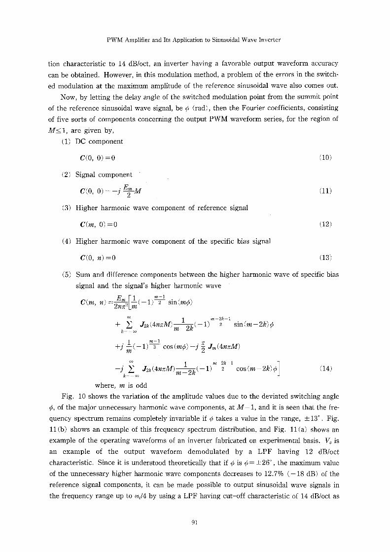
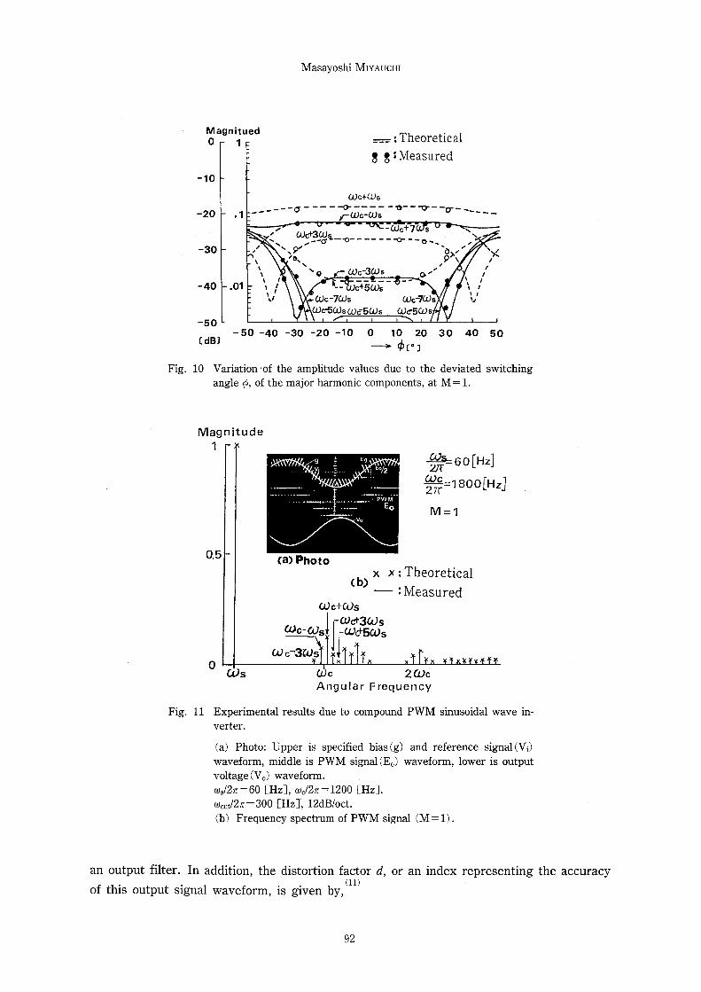
Fig. 10 shows the variation of the amplitude values due to the deviated switching angle
Åë, of the major unnecessary harmonic wave components, at M=1, and it is seen that the fre-
quency spectrum remains completely invariable if ip takes a value in the range, Å}130 . Fig.
11(b) shows an example of this frequency spectrum distribution, and Fig. 11(a) shows an
example of the operating waveforms of an inverter fabricated on experimental basis. Vo is
an example of the output waveform demodulated by a LPF having 12 dB/octcharacteristic. Since it is understood theoretically that if ip is ip= Å}260 , the maximum value
of the unnecessary higher harmonic wave components decreases to 12.7oro (-18 dB) of the
reference signal components, it can be made possible to output sinusoidal wave signals in
the frequency range up to to,/4 by using a LPF having cut-off characteristic of 14 dB/oct as
91
Masayoshi MiyAucm
Magnituedo
-10
-20
-30
-40
-5o[dB)
1
,1
- .Ol
88:
:
Theoretical
Measured
coc+cvs---"- a - --- 7ca-.: di; -e- -v- -cr .. .- .--
1'
N
s s
' t:tN N N
cvc+3 cos t.-cr -- v- -- -- -Nptte. N No c,oc-3CVs
-cvct7
-- o- s-- o .-
o.
s
/
st8>(t
N XK'
Xt lt
v
N s>ct,
tt
t
stsllst
- ---..- -- - c+ 5 CVs
CVc-7CVstuc"5tuscoc'5tos
- --
coc-7tus
toe5tos
Fig.
`
-50 -40 -30 -20 -10 O 10 20 30 40 50 --"-)- (jb[e]
10 Variation•of the amplitude values due to the deviated switching angle ip, of the major harmonic components, at M= 1.
Fig.
Magnitude 1
O,5
o
rfCc26o[Hz]
:l!ll =isoo[HzJ
M=1
11 Experimental results in- verter.
(a) Photo: Upper is specified bias(g) and reference signal(Vi) waveform, middle is PWM signal(E,) waveform, lower is output voltage(V,) waveform. tu,/2z :60 [Hz], to,/2z=1200 [Hz]. to.t12z=:300 [Hz]', 12dB/oct.
(b) Frequency spectrum of PWM signal (M =1).
x x Theoretical (b) Measured wc+Ws.[lllillii.a."'sificawcte3sw.s.
Wc 2CVc Angular Frequency
due to compound PWM sinusoidal wave
anof
output filter. In addition, the
this output signal waveform,
distortion factor d, or an (11)is given by,
index .representmg the accuracy
92
PWM Amplifier and Its Application to Sinusoidal Wave Inverter
oo oo oo Z {ÅíC(m, O) }2+ Z Z {eC(m, n) }2
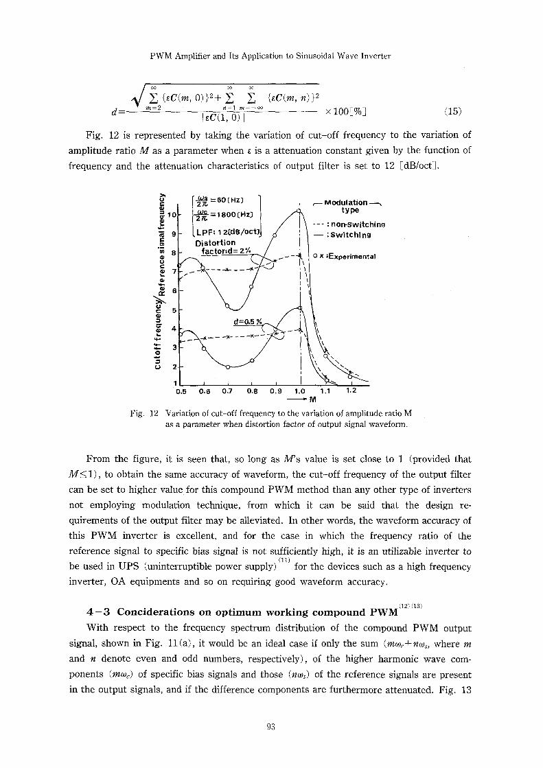
d- M=2 l,c(1",=6 )l!1=-OO xlOO[9J{,] as) Fig. 12 is represented by taking the variation of cut-off frequency to the variation of
amplitude ratio M as a parameter when 6 is a attenuation constant given by the function of
frequency and the attenuation characteristics of output filter is set to 12 [dBloct].
vh
8 glo
2•
gg i9m s
sg.7
<.ec6
g,s
g,4tS'3
oi
gere =60 CHz)
get =1800(Hz)
LPF: 1 2CdB!oct)
Distortion fac tor;d= 2 e/.
- --- .. -- ajt e'
,
ft
-
d=o.s o/.
•-4 .-- - -x- -- -x-- J
t ,t-' tx
tN ll
,
k '",
l,
l,
l
t
t
,
1
r-- Modutation --A type--- ; noftswitching- : switchlng
O x :Experimental
N NNX
NN
x
x
N
xx x x N Ns
Fig.
O.5 O.6 O.7 O.8 O.9 1.0 1.1 1.2 ----M12 Variation of cut-off frequency to the variation of amplitude ratio M
as a parameter when distortion factor of output signal waveform.
From the figure, it is seen that, so long as M's value is set close to 1 (provided that
Ms:1), to obtain the same accuracy of waveform, the cut-off frequency of the output filter
can be set to higher value for this compound PWM method than any other type of inverters
not employing modulation technique, from which it can be said that the design re-
quirements of the output filter may be alleviated. In other words, the waveform accuracy of
this PWM inverter is excellent, and for the case in which the frequency ratio of the
reference signal to specific bias signal is not sufficiently high, it is an utilizable inverter to (11)be used in UPS (uninterruptible power supply) for the devices such as a high frequency
inverter, OA equipments and so on requiring good waveform accuracy.
(12) (13) 4-3 Conciderations on optimum working compound PWM With respect to the frequency spectrum distribution of the compound PWM output
signal, shown in Fig. 11(a), it would be an ideal case if only the sum (mtoc+ntus, where m
and n denote even and odd numbers, respectively), of the higher harmonic wave com-
ponents (mtoc) of specific bias signals and those (ntos) of the reference signals are present
in the output signals, and if the difference components are furthermore attenuated. Fig. 13
93
Masayoshi MIyAucHI
Lt
Eg Ei Eg2 Eor o
Ems.2o
Fig.
gtÅë)
acos
vi(t) 2rr3T,
arrRl
' :f
-
zacoclMp=RofRi"
I-.PW
':Eo(t
--.s
13 Operation principles of sinusoidal inverter.
OPtlMUMworking compound
t
t
PWM
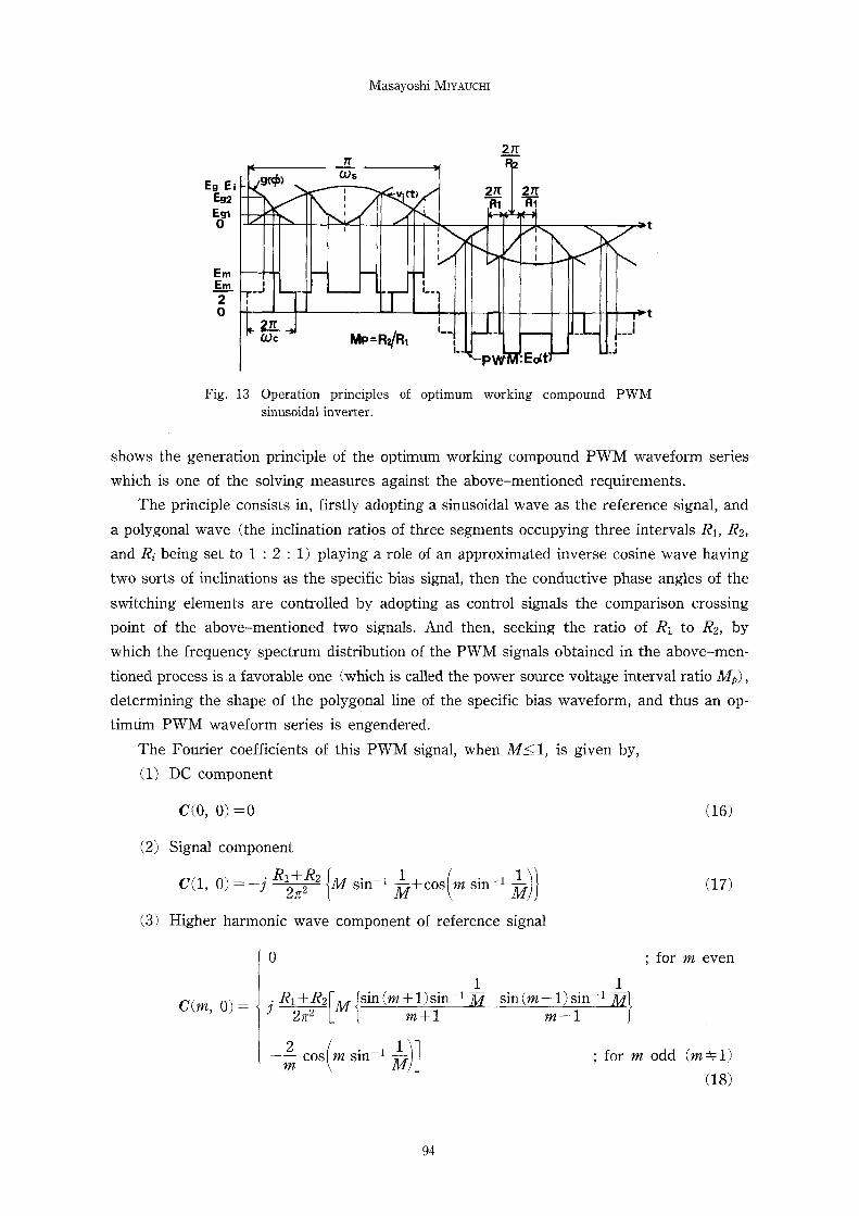
shows the generation principle of the optimum working compound PWM waveform series
which is one of the solving measures against the above-mentioned requirements.
The principle consists in, firstly adopting a sinusoidal wave as the reference signal, and
a polygonal wave (the inclination ratios of three segments occupying three intervals Ri, R2,
and Ri being set to 1:2: 1) playing a role of an approximated inverse cosine wave having
two sorts of inclinations as the specific bias signal, then the conductive phase angles of the
switching elements are controlled by adopting as control signals the comparison crossing
point of the above-mentioned two signals. And then, seeking the ratio of Ri to R2, by
which the frequency spectrum distribution of the PWM signals obtained in the above-men-
tioned process is a favorable one <which is called the power source voltage interval ratio Mp) ,
determining the shape of the polygonal line of the specific bias waveform, and thus an op-
timitm PWM waveform series is engendered.
The Fourier coefficients of this PWM signal, when MSI, is given by,
(1) DC component
c(o,
(2) Signal
C(1,
(3) Higher
o) -o
component
o) = v' Riin2R2 (M sin-i ?iZ+cos(m sinnti
harmonic wave component of reference
C(m, O) =
o
j R,+R2[M( !sin(m+1)sin-i
M))
signal
sin(m-1)sin-i1
M}; for m
(16)
(17)
even
2n2
-ilili cos(m
m+1sin-i ?l))]
m-1
; for m odd (m \1)
(18)
94
PWM Amplifier and Its Application to Sinusoidal Wave Inverter
(4) Higher harmonic wave component of the specific bias signal
C(O, n) =O (19) (5) Sum and difference components between the higher harmonic wave of specific bias
signal and the signal's higher harmonic wave
O 'formeven '
C(m, n)= ]'2 :2[il} (sin{m sinm'(2 (RRii++2R5)2M)+nRi} ;for m odd
'sin{m sin-i(2 (Ri5iR2)M)-nRi}+sin(m sin'i ?l})]
ve sinTi(2 (R, 5'R,) M) Jm {2 (Ri +R2) nM}
- le =;i .. Jk {2 (Ri +R2) nM} .!k sin{ (m -k) sin-i(2 (R, +R'R,) M) }
le:\m -2 cos(Z Ri) ({sinNi(2 (RRi,++2R5)2M) -sinrm'(2 (Ri+R'R2)M)}
• Jm { (Ri + R2) nlva +, ..Si .. Jk { (Ri +R2) nM} .I le
k#m • sin{ (m - le) sin"i(2 (RRi, ++ 2R5)2M) } u sin { (m - le) sin un '(2 (R, 5iR,) M) })
+ 2 sin (Z Ri), =Sl .. Jfe { (Ri + R2) nM} . ! le
k\m • (cos{ (m-k) sinmi (2 (RRii ++ R2f)2M) } - cos{ (m -k) sinri (2 (Ri +Ri 2) M) }l
+ cos (nR2) ({sin rr i(2 ("Rl?ii ++ 2R{ll3M) - sinr i ]li} J. {2 (Ri + R2) nM}
+k=;i .. Jk {2 (Ri +R2) nM} m 1- le sin{ (m - k) sin rr i (2 (RRii ++ 2R5)2M) }
-sin{(m-k)sinLi ihF}]
+ sin (nR2) fe ..jli .. Jfe {2 (Ri + R2) nM} ml le
k#m • (cos{(m-k)sin-i(2 (Rii ++2R5)2M)}-cos{(m-k) sin-i 71}}) ]
(20)
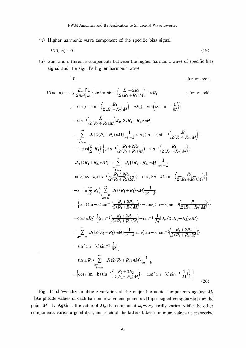
Fig. 14 shows the amplitude variation of the major harmonic components against Mp
( LAmplitude values of each harmonic wave components 11iInput signal components D at the
point M=1. Against the value of Mp the component oc-3tus hardly varies, while the other
components varies a good deal, and each of the latters takes minimum values at respective
95
Masayoshi MIyAucHI
two points, and when Mp=3.72, the average values of each component takes their respec-
tive minimum values. However, when the value of Mp lies in the range 3.72-J4.52, com-
ponents tuc-5tu, and toc-7tus do not vary too much and component toc-tus takes a minimum
value, which leads to a practicable selection of the components' values against the range of
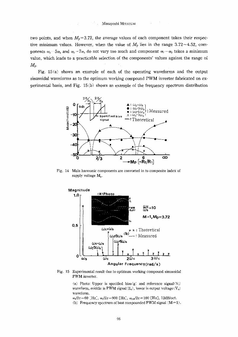
Mp• ' Fig. 15(a) shows an example of each of the operating waveforms and the output 'sinusoidal waveforms as to the optimum working compound PWM inverter fabricated on ex-
perimental basis, and Fig. 15(b) shows an example of the frequency spectrum distribution
Fig.
Atx)
vv
B.e-.
kE
2YRa>2%2o AN :cvc-cDs
eI'cacoc.i3coav,S:Measured
-10
-20signal
.-Specified
A
xbias-:;cvc-7cvs
TheoreticalA
-30
-40 -
x
- o 2/3 2- 6Mp[=R2/Ri] co
14 Main harmonic components are convorted in to composite index of supply voltage M,.
Magnitude (a)Photo 1.0
O.5 cvc+CDs
coct3cvs
COc-CL)scoc-3• cVs L
i
PWMEcit}
vo
xx(b)
iCVCt5cv,
:
:
{Sgt =1o
M=1,Mp=3.72
Theoretical
Measured
Fig.
o cas coc 2toc 3CL)c Angular Frequency(rad/s)
15 Experimental result due to optimum working compound sinusoidal PWM inverter.
(a) Photo: Upper is specified bias(g) and reference signal(Vi) waveform, middle is PWM signal(E,), lower is output voltage(Vo)
waveform. tu,12n==60 [Hz], tu,/2n=900 [Hz], to,.t12n =100 [Hz], 12dBloct.
(b) Frequency spectrum ofbast compounded PWM signal (M =1).
96
PWM Amplifier and Its Application to Sinusoidal Wave Inverter
measured thereof. "X" marks in the figure denote theoretical values, and since they coin-
cide well with the measured values, the validity of our theory is confirmed. The measured
values of each component at the optimum pattern (M=1, Mp=3.72), of the output signals
against the corresponding reference signal components take such values as tuc+tos=:-6.7
dB, toc-tus= -40.0 dB, tuc-3ws= -36.3 dB, and tu,-5bls=-45.1 dB. It is seen that compo-
nent tuc-3tos is somewhat large, but all of the differences of harmonic waves' components
between the other specific bias signals and the reference signals are -40 dB or lower.
From these facts, so long as M takes a value close to 1 (O.9<M<1.05), since the upper
limit frequency of the reference signal is confined by the component's difference [cac-3tos]
between the harmonic wave of specific bias signal and the odd number higher harmonic
waves, more improvement of the dynamic range, compared with the case of the compound
PWM sinusoidal wave inverter shown in Fig. 7, can be achieved, leading to the applicabili-
ty to higher frequency devices.
5. Conclusion
Basic principles and representative configuration methods of PWM amplifiers have
been presented, their frequency spectra were obtained by expanding the PWM signals, on
the occasion when the input signals are confined to sinusoidal waves, in double Fourier
series, and the characteristics thereof were described. Especially, the two stage PWM
sinusoidal wave amplifier, in which the pulse width is switched over from the leading edge
to trailing edge, or to leading edge modulation, makes possible the lowering of the
amplitudes of unnecessary harmonic wave components, and also the enlargement of the
dynamic range (the upper limit value of input sinusoidal wave frequency), which proved
the applicability of the present amplifier as inverter.
Next, we proposed a compound PWM sinusoidal wave inverter which is a logically ex-
tended version of the two stage PWM sinusoidal wave amplifier employing this switched
modulation method. From the studies on theoretical analyses and the experimental results
based on the devices prepared by trial fabrication, it was clarified that the basic
characteristics of the new inverter provide sinusoidal wave output having very low distor-
tion rate, and that it is effectively applicable to CVCF (constant voltage-constant freq-
uency) device and also to UPS (uninterruptible power supply) for OA appliances.
Moreover, we have replaced the specific bias signal waves in this compound PWM
method with a polygonal line waveforms (using a sawtooth waveforms with differently in-
clined segrnents) having two sorts of inclinations approximated to inverse cosine function,
and made propositions and studies on the models made by trial fabrication concerning the
optimum compound PWM method in which upwardly convex type DC power source voltage
is adopted. From these studies it was shown that, since the upper limit frequency of the
reference sinusoidal waveform signal is confined by the difference between the harmonic
components of the secondary specific bias signal (carrier signal) and the odd number
97
Masayoshi•MIyAucHi
higher harmonic components of the reference signal to delimit the upper frequency at tu,-3
w,, which facilitates the configuration of the output filter (LPF), and that it is applicable to
inverters for high frequency circuit devices in which the frequency ratio of the reference
signal to carrier signal cannot be set to a large number. Moreover, by means of the
sinusoidal wave approximation of DC power source voltage using this optimum compound
PWM method, it is possible to realize as the unnecessary harmonic wave 'components of a
certain PWM signal such that the former comprise only the components' sum of the two
signals, i.e., odd number harmonic waves of the reference signal and the harmonic waves of
carrier signal. However, as to this proposed new scheme, it will later be reported in
another paper, together with VVVF(variable voltage, variable frequency) method in which
the reference signal itself varies, and also with the development of an inverter in which fur-
-ther multiplexing techniques are applied to PWM.
Finally, the authors express sincere gratitude to Prof. Shukichi Kaku (Osaka Institute
of Technology) who participated in the discussion of the present research and gave us
valuable advices.
References'
(1) H. S. Black.: Modulation theory, van Nostrand 1966
(2) S. Kaku, S. Minamoto & K. Miyakosi.: "Generalized analysis of output signal of switched mode
amplifier". Bull. of Univ. of Osaka Pref., A-15, 119(1966)
(3) S. Minamoto, K. Nohara & K. Miyakosi.: "Soltd-state thyratron arnplifier". Bull. of Univ. of Osaka
Pref., A-11, 55(1962)
(4) S. Kaku. "Output filter for thyristor amplifier". J. Inst. Elec. Eng. (Tokyo). vol. 89, No. 7,
27(1969) (5) S. Kaku. "Swithing-mode absolute-value amplifier and its applications". IEEE Trans. IM 25.
79 (1976)
(6) M. Miyauchi. "Swithing-mode absolute-value amplifier and its applications -Traianguler-wave
multiplier and arbitrary function generator-". Bulletin of the Japan Society of Industrial and
Technical Education, Vol. 20, No. 1(1978)
(7) M. Miyauchi.: "PWM Operational Amplifier", Mem. Fac, Educ. Ehime Univ., Nat. sci, Vol. 14, No.
1, 49(1993) • (8) I. B. Huang & W. S. Lin. "Harmonic reduction in inverter by use of sinusoidal pulse width modula-
tion", IEEE Trans. Ind. Ele. Com. Instrum, IECI-27, 201(1970)
(9) D. A. Grant.: "Ratio changing in pulse-width-modulated inverter", IEEE Proc. B. Elect. P. Aplli.
128-5, 242(1981)(10) I. Yamamoto, T. Yamauchi, S. Kaku & M. Miyauchi.: "Compounded PWM sinusoidal amplifier",
Proc. 28th SICE Annual Conf., Vol. 1, JS8-2(1989)
(11) L. Hampson.: "PWM uninterruputable power supplies", Electronic Components and Applications.
Vol. 4, No.2(February 1982) '(12) M. Miyauchi & Y. Honda.: "Compound PWM sinusoidal amplifier", Proc, 33th, Jap. Soci. Ind., and
Tec, Educ. Conf., No. 401(1990)
(13) M. Miyauchi.: "Compound PWM sinusoidal inverter", Proc, 35th, Jap. Soci. Ind., and Tec. Educ.
Conf., No. 308(1992)
98