Embed Size (px)
Citation preview
Nanomaterials and AnalyticsSemiconductor Nanocrystals and Carbon Nanotubes
- Introduction and Preparation- Characterisation
- Applications
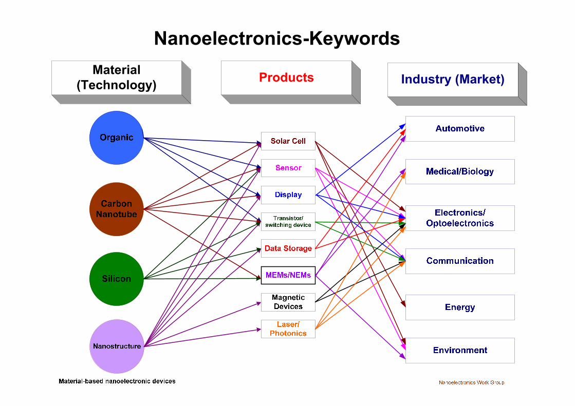
Schematic Structure of a QD Laser
n+ GaAs Substrate
n+ GaAs Buffer 0.5 μm
n+ GaAs/AlAs Superlattice
n Al0.65Ga0.35As 1.6 μm
p Al0.65Ga0.35As 1.6 μmp GaAs/AlAs Superlattice
p+ GaAs 0.15 μm
p AlxGa1-xAs Grading
n AlxGa1-xAs Grading
GaAs 100 nm
GaAs 100 nm
GaAs30 nm
1100 1200 1300 1400 1500EL
Inte
nsity
26oC 85oC 100oC
Wavelength (nm)1100 1200 1300 1400
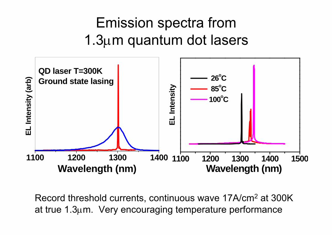
QD laser T=300KGround state lasing
EL In
tens
ity (a
rb)
Wavelength (nm)
Emission spectra from 1.3μm quantum dot lasers
Record threshold currents, continuous wave 17A/cm2 at 300K at true 1.3μm. Very encouraging temperature performance
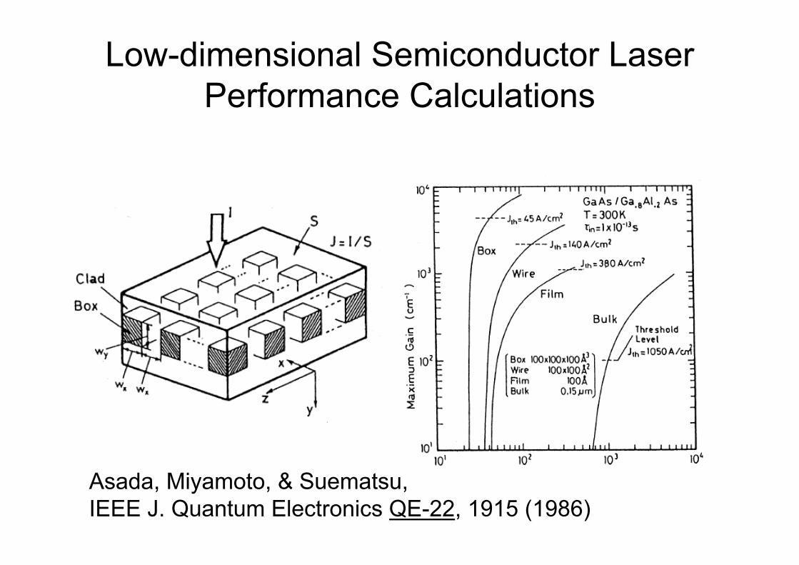
Low-dimensional Semiconductor LaserPerformance Calculations
Asada, Miyamoto, & Suematsu,IEEE J. Quantum Electronics QE-22, 1915 (1986)
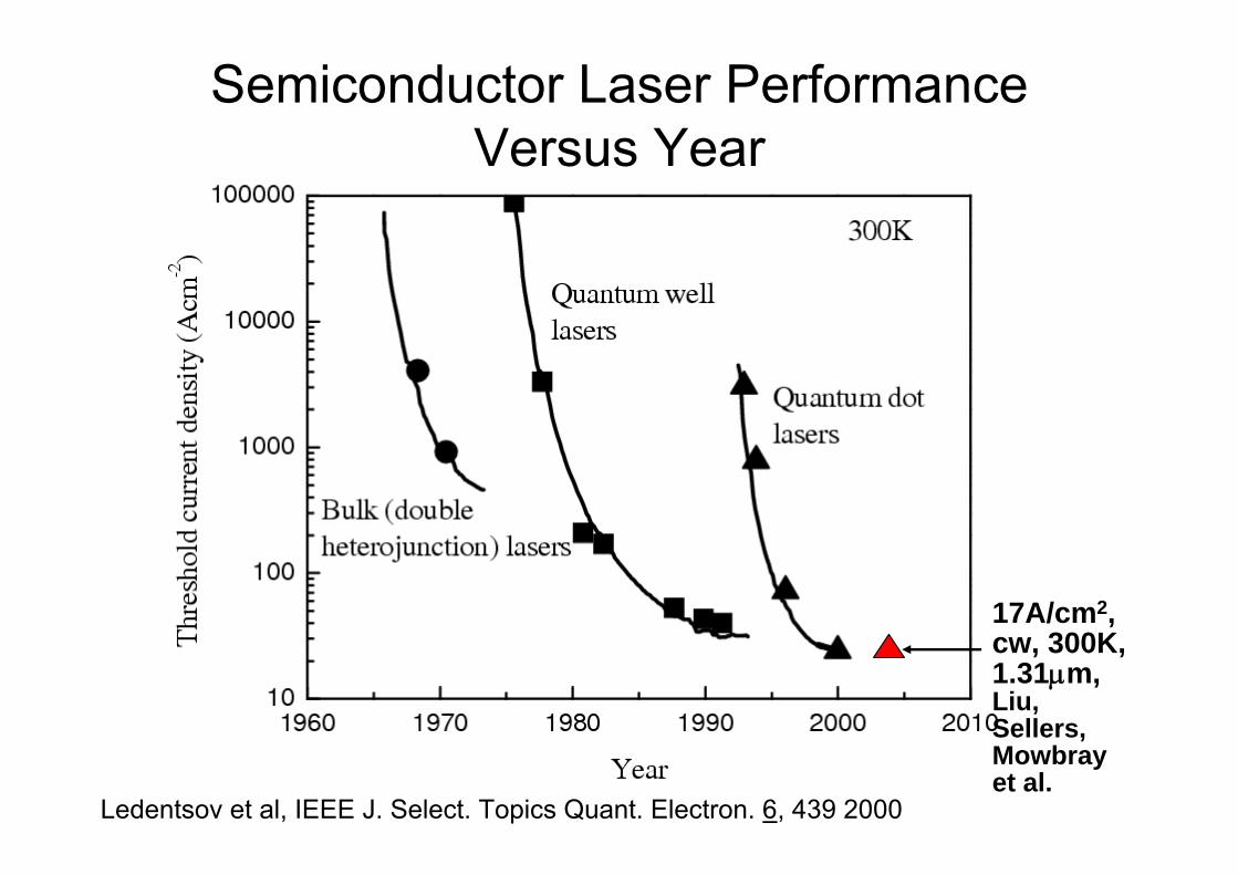
Semiconductor Laser Performance Versus Year
Ledentsov et al, IEEE J. Select. Topics Quant. Electron. 6, 439 2000
17A/cm2, cw, 300K, 1.31μm, Liu, Sellers, Mowbray et al.
Why a Quantum Dot Solar Cell ?
Core/Shell dots high luminescence ηSemiconductor should not degradeSingle molecule precursor dots cheapAbsorption shift tuned by dot sizeSpread fixed by growth conditionsRe-absorption can be maximised
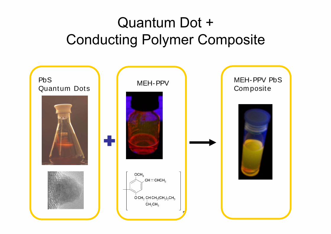
Quantum Dot + Conducting Polymer Composite
PbSQuantum Dots
MEH-PPV MEH-PPV PbSComposite
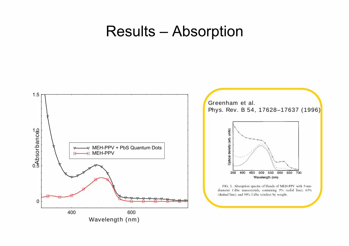
Results – Absorption
Greenham et al. Phys. Rev. B 54, 17628–17637 (1996)
Wavelength (nm)
Abs
orba
nce
0
0.5
1.0
1.5
400 600
MEH-PPV + PbS Quantum DotsMEH-PPV
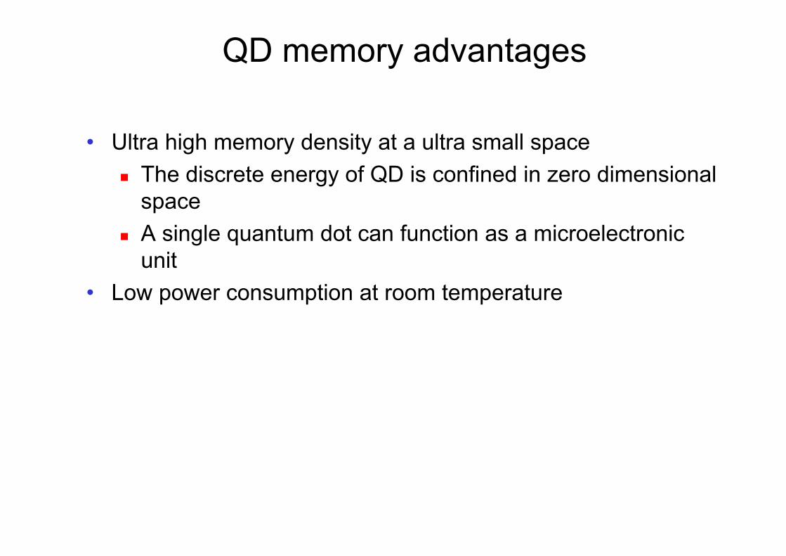
QD memory advantages
• Ultra high memory density at a ultra small space The discrete energy of QD is confined in zero dimensional spaceA single quantum dot can function as a microelectronic unit
• Low power consumption at room temperature
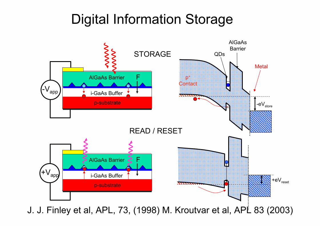
+eVreset
READ / RESET
p-substrate
i-GaAs Buffer
AlGaAs Barrier F
+Vapp
-eVstorep-substrate
i-GaAs Buffer
AlGaAs Barrier F
STORAGE
-Vapp
p+
Contact
Metal
AlGaAsBarrier
QDs
Digital Information Storage
J. J. Finley et al, APL, 73, (1998) M. Kroutvar et al, APL 83 (2003)
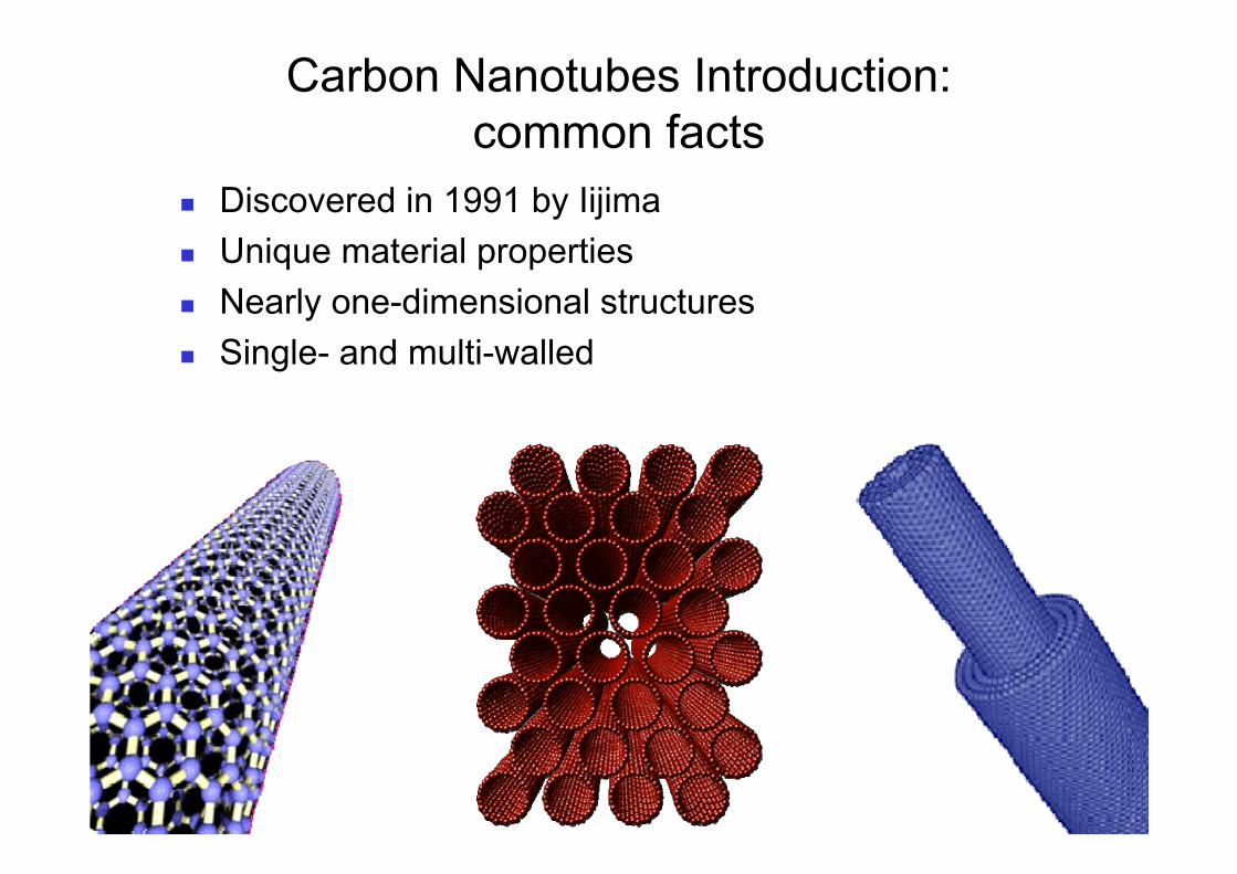
Carbon Nanotubes Introduction: common facts
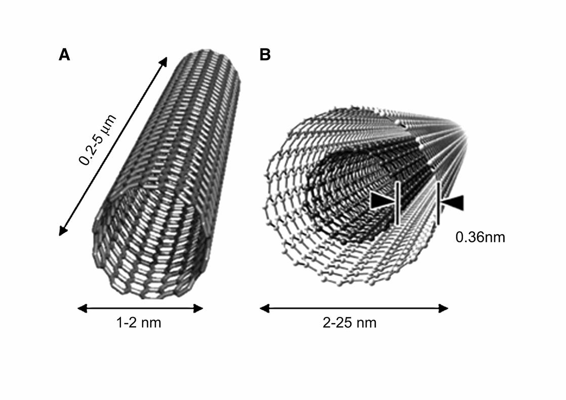
Discovered in 1991 by IijimaUnique material propertiesNearly one-dimensional structuresSingle- and multi-walled
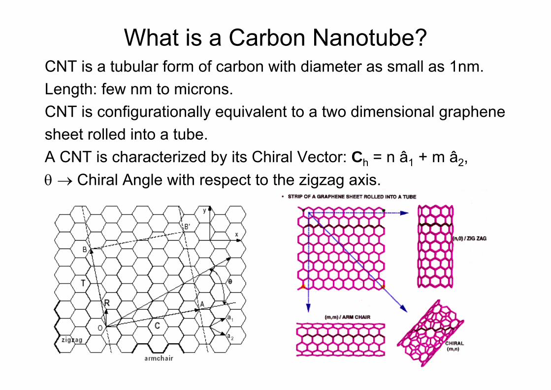
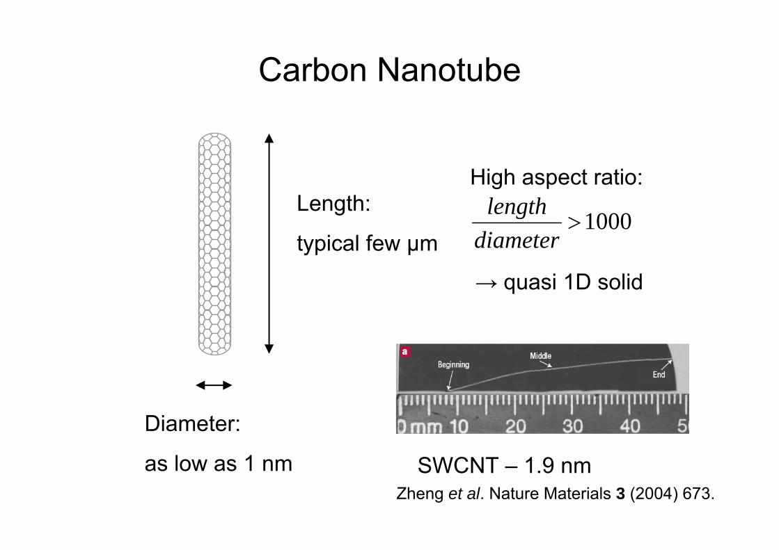
What is a Carbon Nanotube?CNT is a tubular form of carbon with diameter as small as 1nm.Length: few nm to microns.CNT is configurationally equivalent to a two dimensional graphenesheet rolled into a tube.A CNT is characterized by its Chiral Vector: Ch = n â1 + m â2, θ → Chiral Angle with respect to the zigzag axis.
Schematicof a CNT
STM imageof CNT
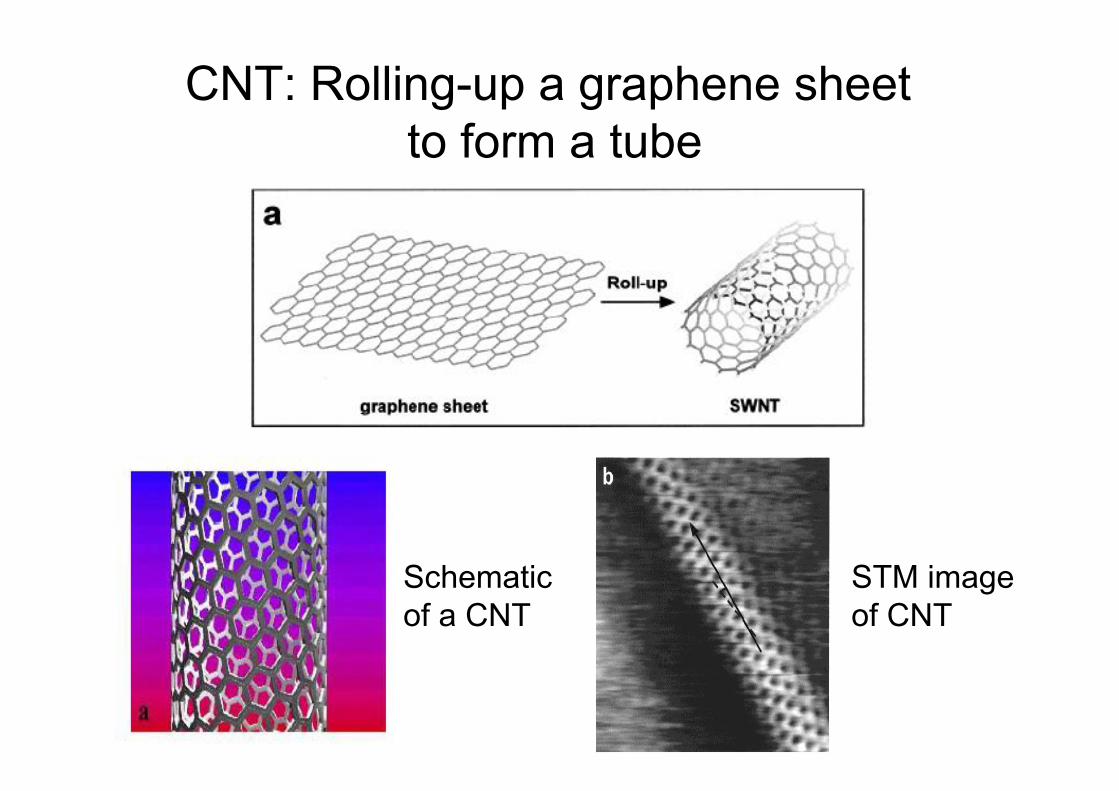
CNT: Rolling-up a graphene sheet to form a tube
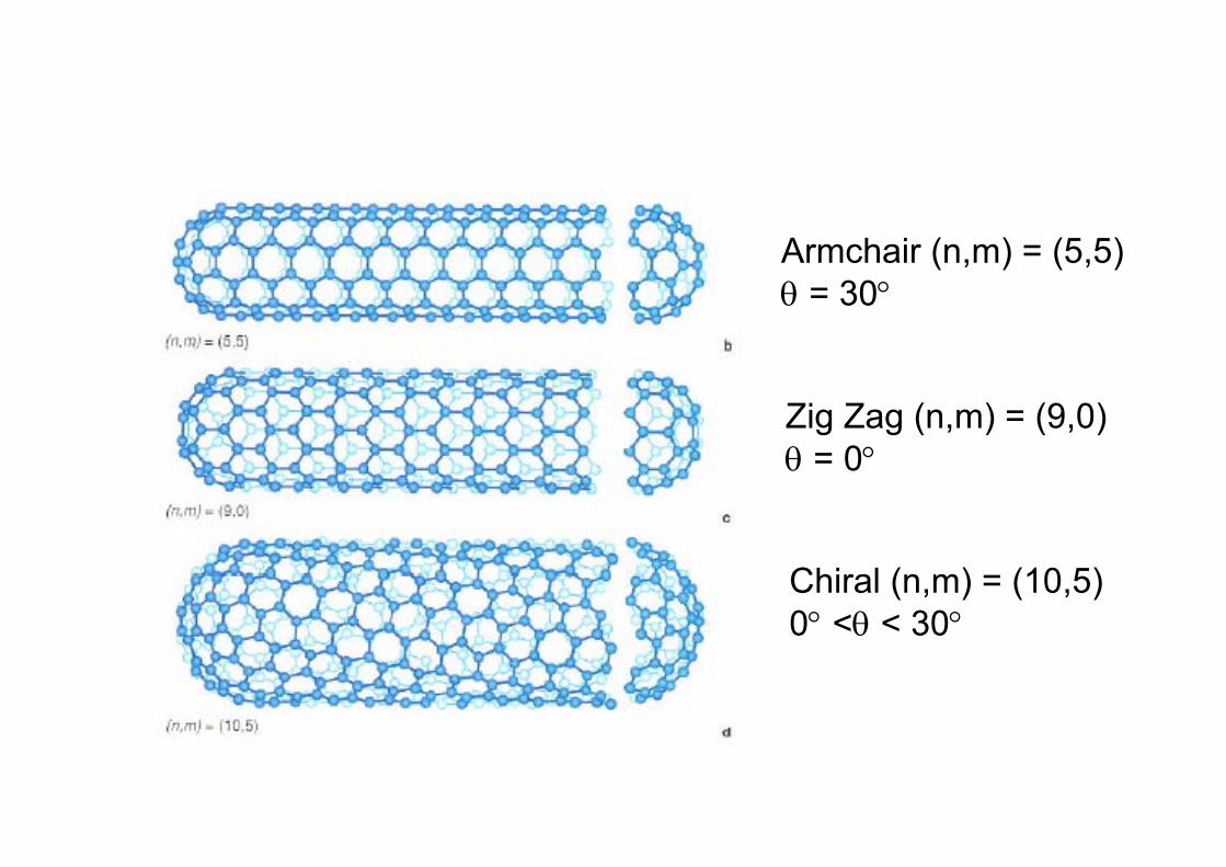
Armchair (n,m) = (5,5)θ = 30°
Zig Zag (n,m) = (9,0)θ = 0°
Chiral (n,m) = (10,5)0° <θ < 30°
Carbon Nanotube
Zheng et al. Nature Materials 3 (2004) 673.SWCNT – 1.9 nm
Diameter:
as low as 1 nm
Length:
typical few μm
High aspect ratio:
1000>diameterlength
→ quasi 1D solid
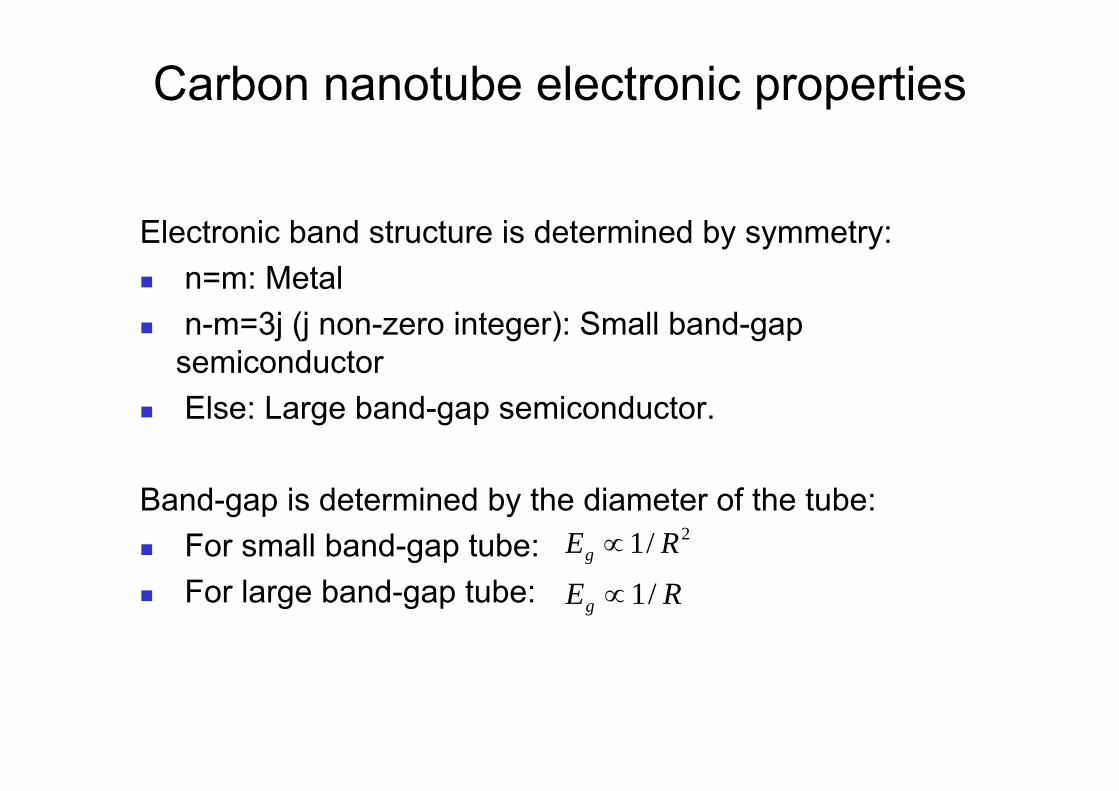
Carbon nanotube electronic properties
Electronic band structure is determined by symmetry:n=m: Metaln-m=3j (j non-zero integer): Small band-gap semiconductorElse: Large band-gap semiconductor.
Band-gap is determined by the diameter of the tube:For small band-gap tube: For large band-gap tube:
2/1 REg ∝
REg /1∝
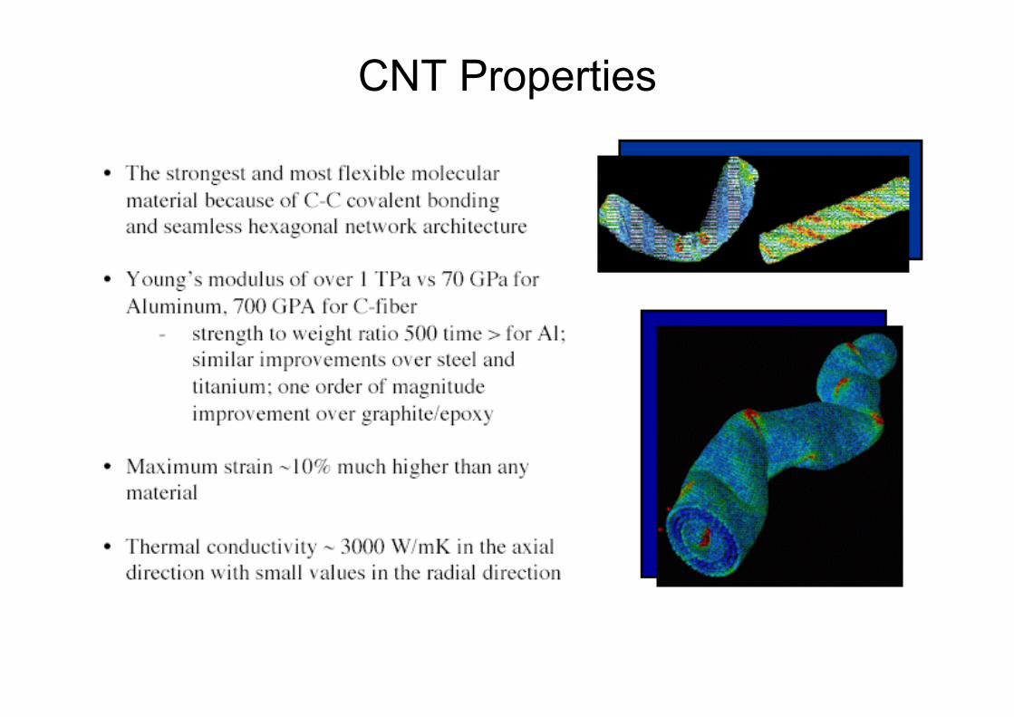
CNT Properties
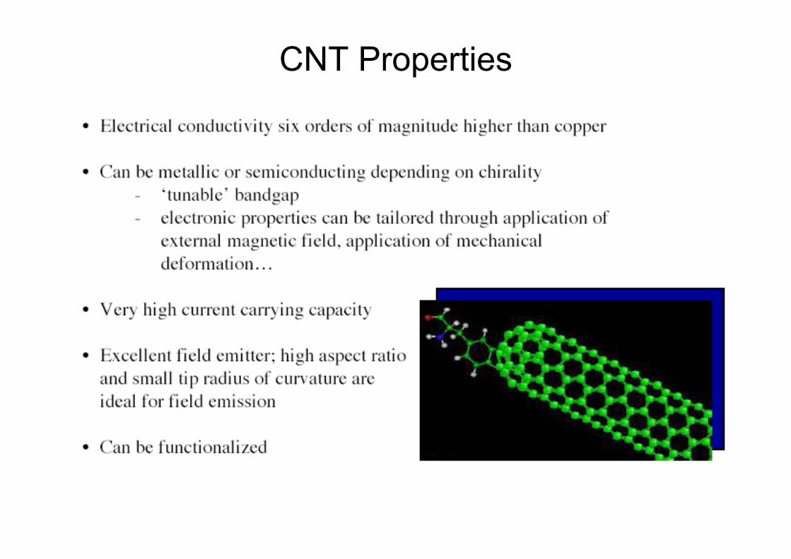
CNT Properties
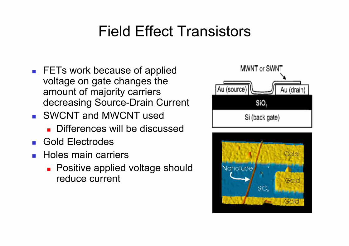
Field Effect Transistors
FETs work because of applied voltage on gate changes the amount of majority carriers decreasing Source-Drain CurrentSWCNT and MWCNT used
Differences will be discussedGold ElectrodesHoles main carriers
Positive applied voltage should reduce current
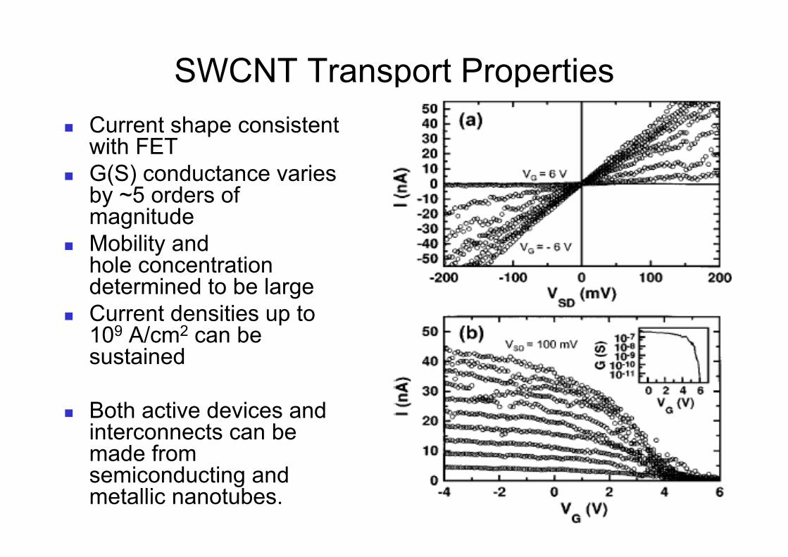
SWCNT Transport PropertiesCurrent shape consistent with FETG(S) conductance varies by ~5 orders of magnitudeMobility and hole concentration determined to be largeCurrent densities up to 109 A/cm2 can be sustained
Both active devices and interconnects can be made from semiconducting and metallic nanotubes.
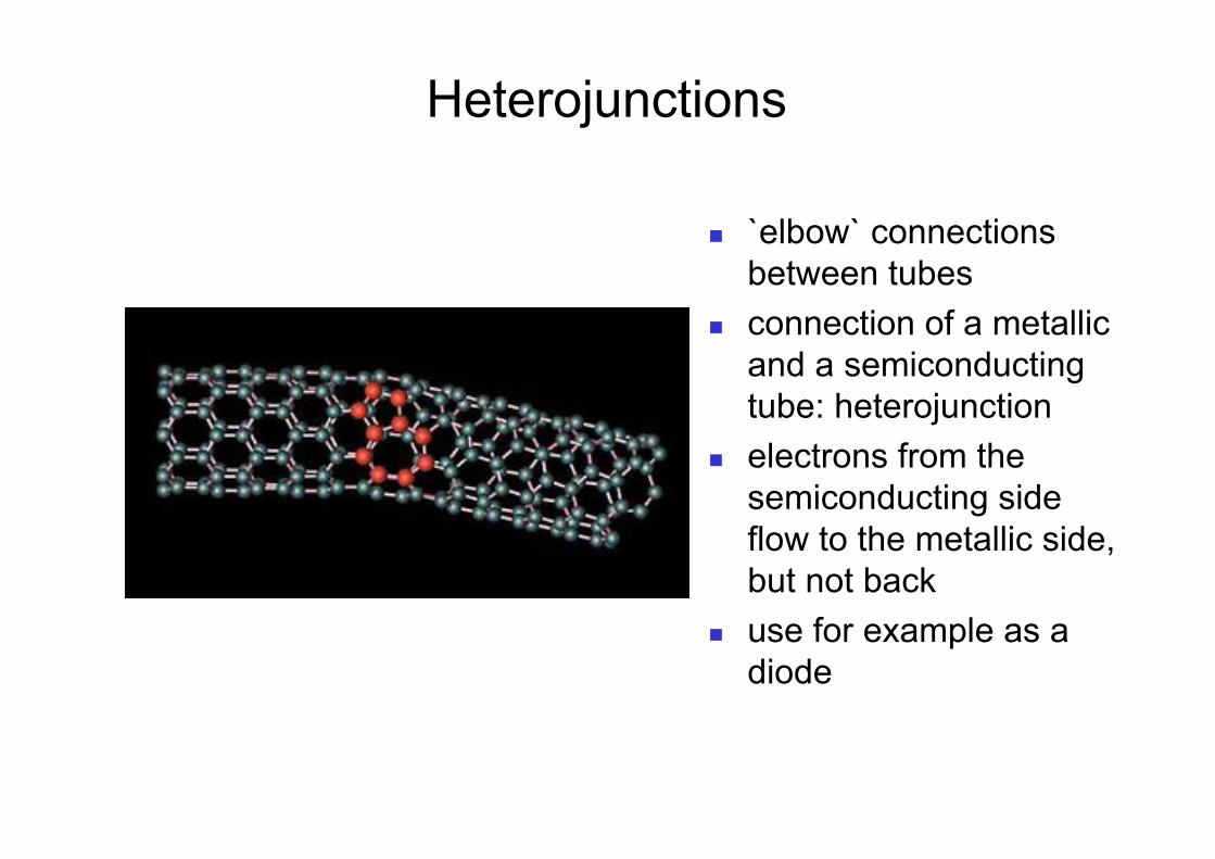
Heterojunctions
`elbow` connectionsbetween tubesconnection of a metallic and a semiconductingtube: heterojunctionelectrons from thesemiconducting sideflow to the metallic side, but not backuse for example as a diode
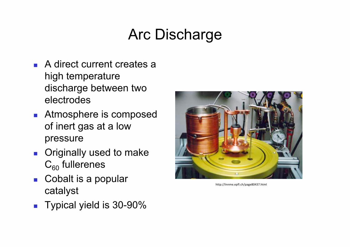
Arc Discharge
A direct current creates a high temperature discharge between two electrodesAtmosphere is composed of inert gas at a low pressureOriginally used to make C60 fullerenesCobalt is a popular catalystTypical yield is 30-90%
http://lnnme.epfl.ch/page80437.html
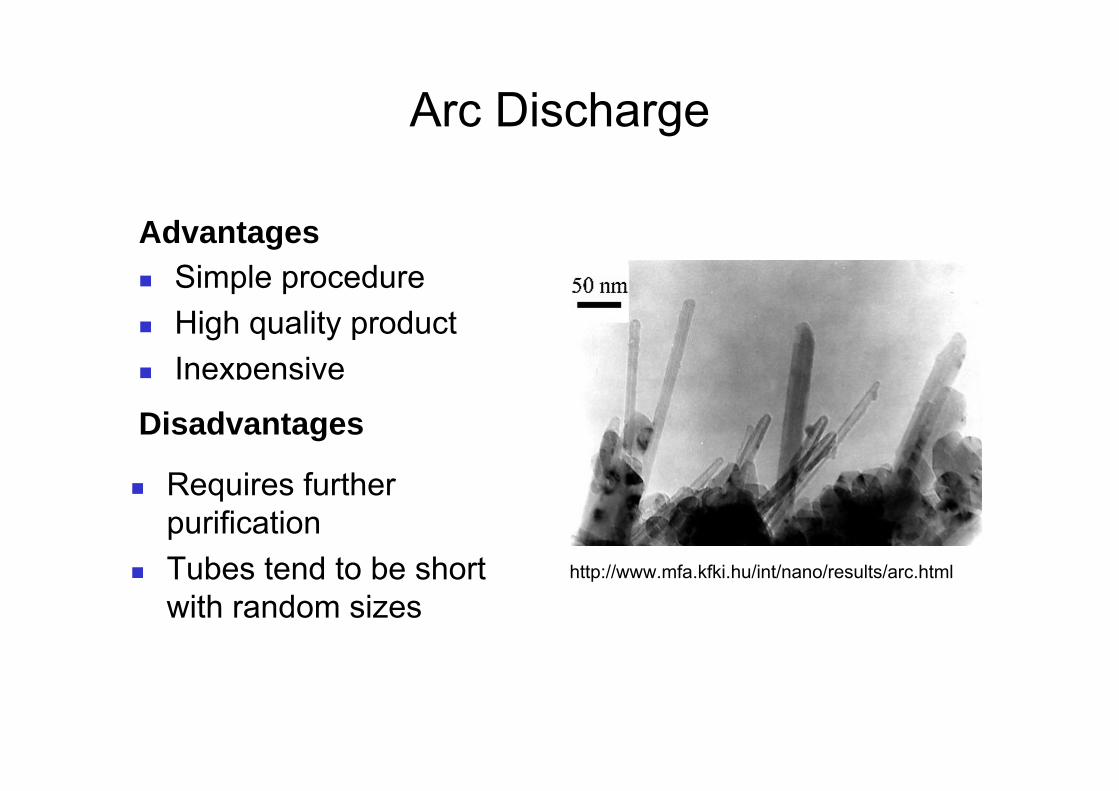
Arc Discharge
AdvantagesSimple procedureHigh quality productInexpensive
Disadvantages
Requires further purificationTubes tend to be short with random sizes
http://www.mfa.kfki.hu/int/nano/results/arc.html
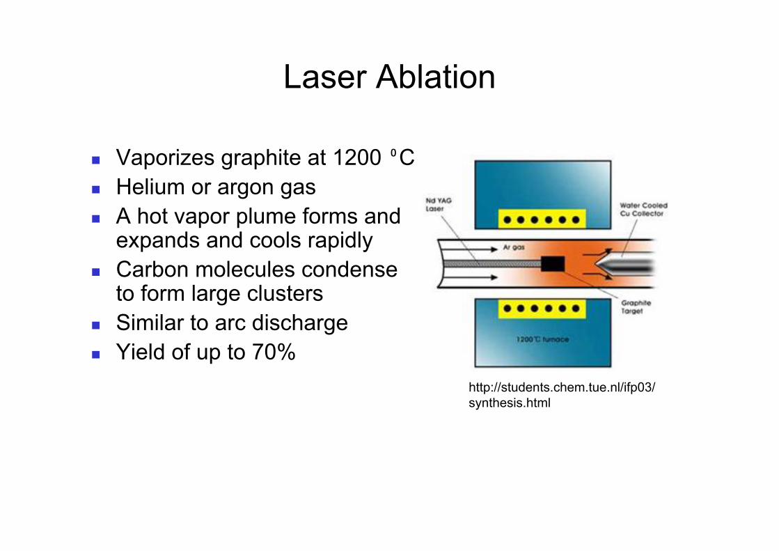
Laser Ablation
Vaporizes graphite at 1200 ⁰CHelium or argon gasA hot vapor plume forms and expands and cools rapidlyCarbon molecules condense to form large clustersSimilar to arc dischargeYield of up to 70%
http://students.chem.tue.nl/ifp03/synthesis.html
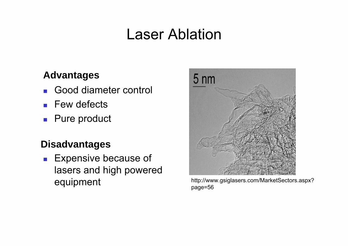
Laser Ablation
AdvantagesGood diameter controlFew defectsPure product
DisadvantagesExpensive because of lasers and high powered equipment http://www.gsiglasers.com/MarketSectors.aspx?
page=56
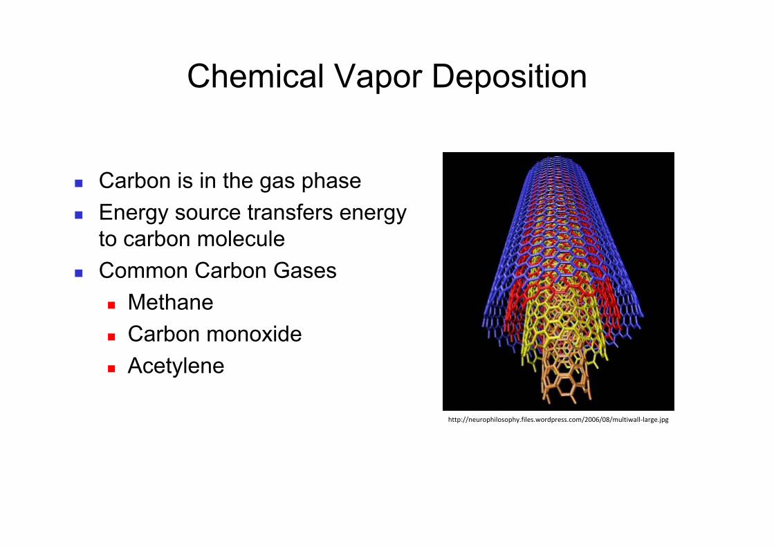
Chemical Vapor Deposition
Carbon is in the gas phaseEnergy source transfers energy to carbon moleculeCommon Carbon Gases
MethaneCarbon monoxideAcetylene
http://neurophilosophy.files.wordpress.com/2006/08/multiwall‐large.jpg
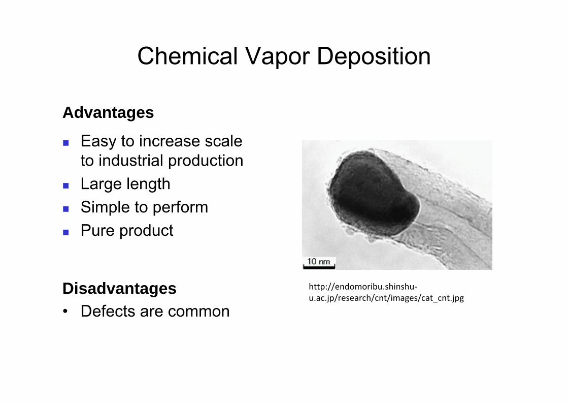
Chemical Vapor Deposition
Advantages
Disadvantages
Easy to increase scale to industrial productionLarge lengthSimple to performPure product
http://endomoribu.shinshu‐u.ac.jp/research/cnt/images/cat_cnt.jpg
• Defects are common
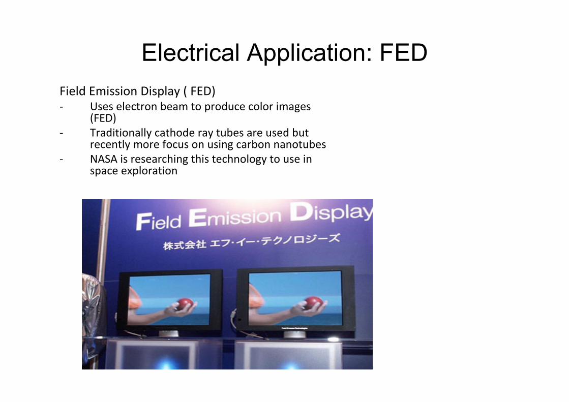
Electrical Application: FEDField Emission Display ( FED)‐ Uses electron beam to produce color images
(FED)‐ Traditionally cathode ray tubes are used but
recently more focus on using carbon nanotubes‐ NASA is researching this technology to use in
space exploration
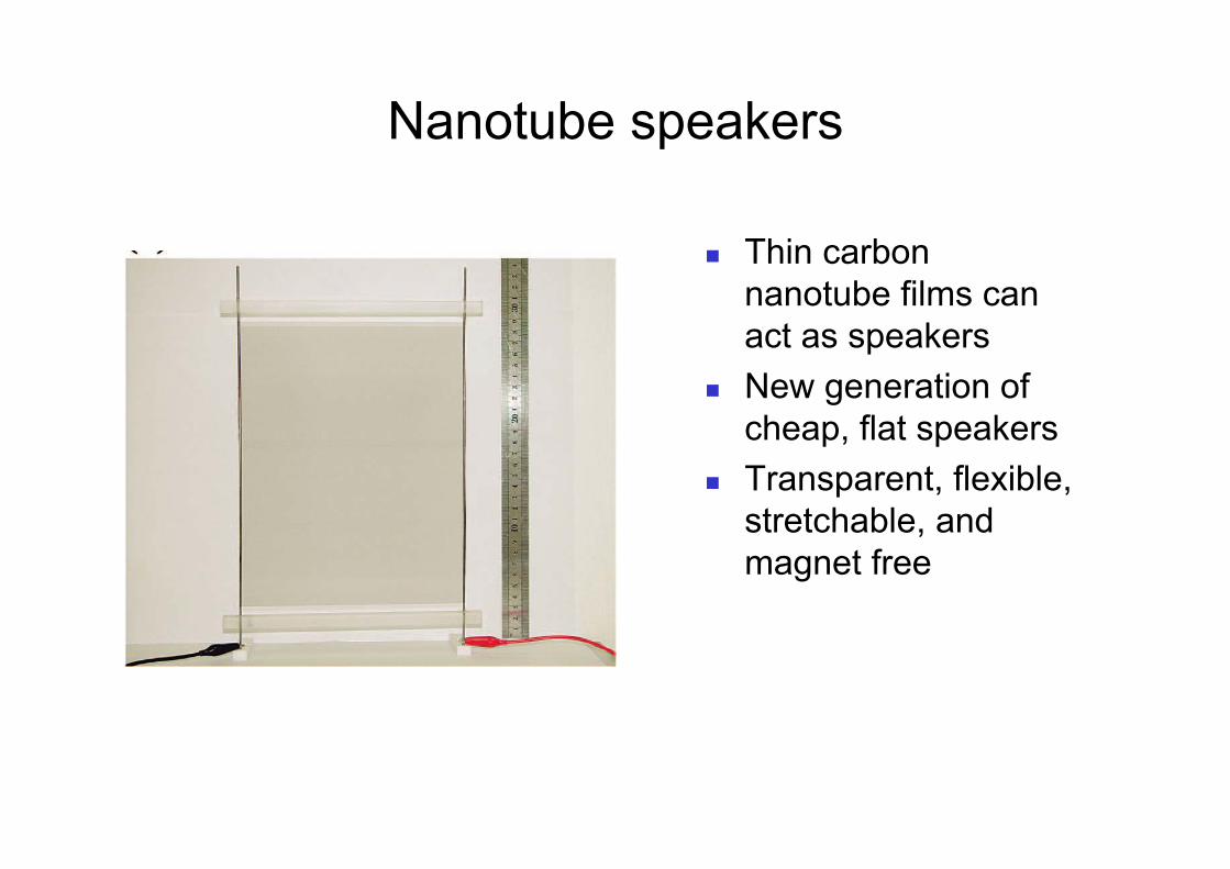
Nanotube speakers
Thin carbon nanotube films can act as speakersNew generation of cheap, flat speakersTransparent, flexible, stretchable, and magnet free
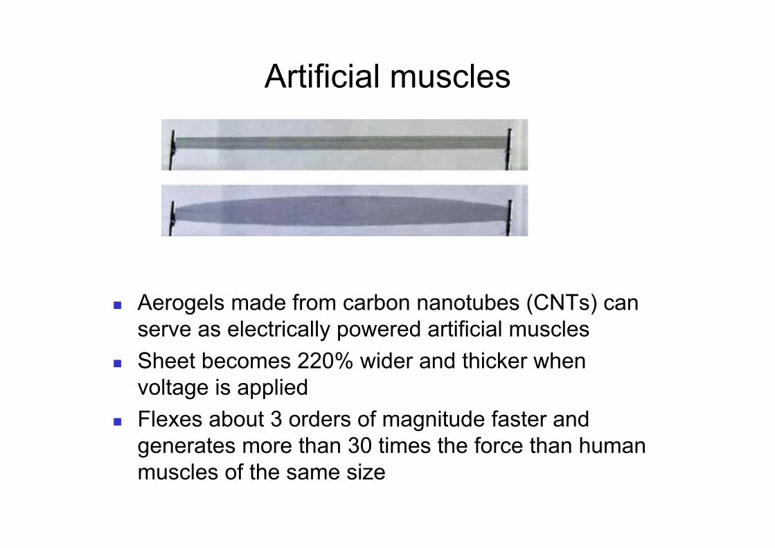
Artificial muscles
Aerogels made from carbon nanotubes (CNTs) can serve as electrically powered artificial musclesSheet becomes 220% wider and thicker when voltage is appliedFlexes about 3 orders of magnitude faster and generates more than 30 times the force than human muscles of the same size
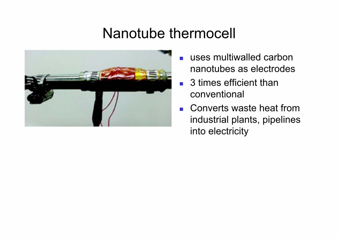
Nanotube thermocelluses multiwalled carbon nanotubes as electrodes3 times efficient than conventionalConverts waste heat from industrial plants, pipelines into electricity
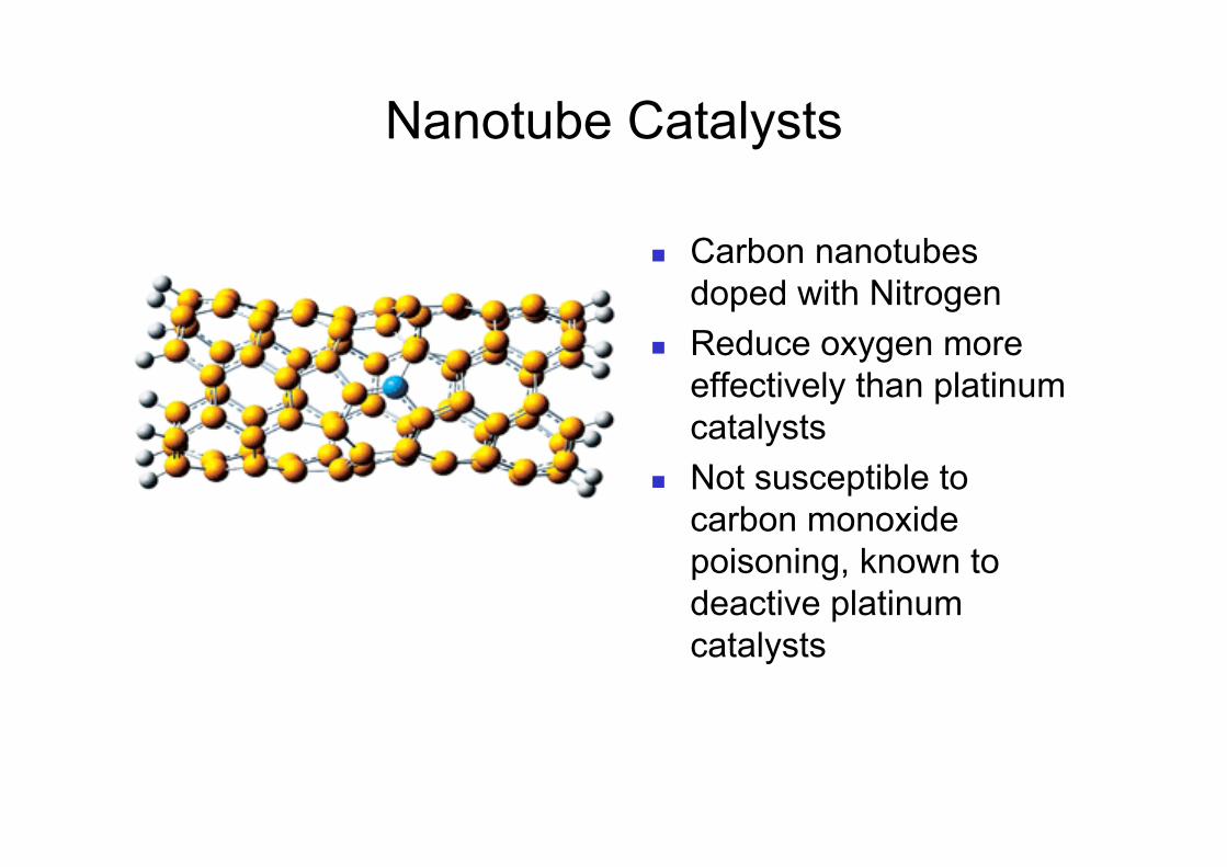
Nanotube Catalysts
Carbon nanotubesdoped with NitrogenReduce oxygen more effectively than platinum catalystsNot susceptible to carbon monoxide poisoning, known to deactive platinum catalysts
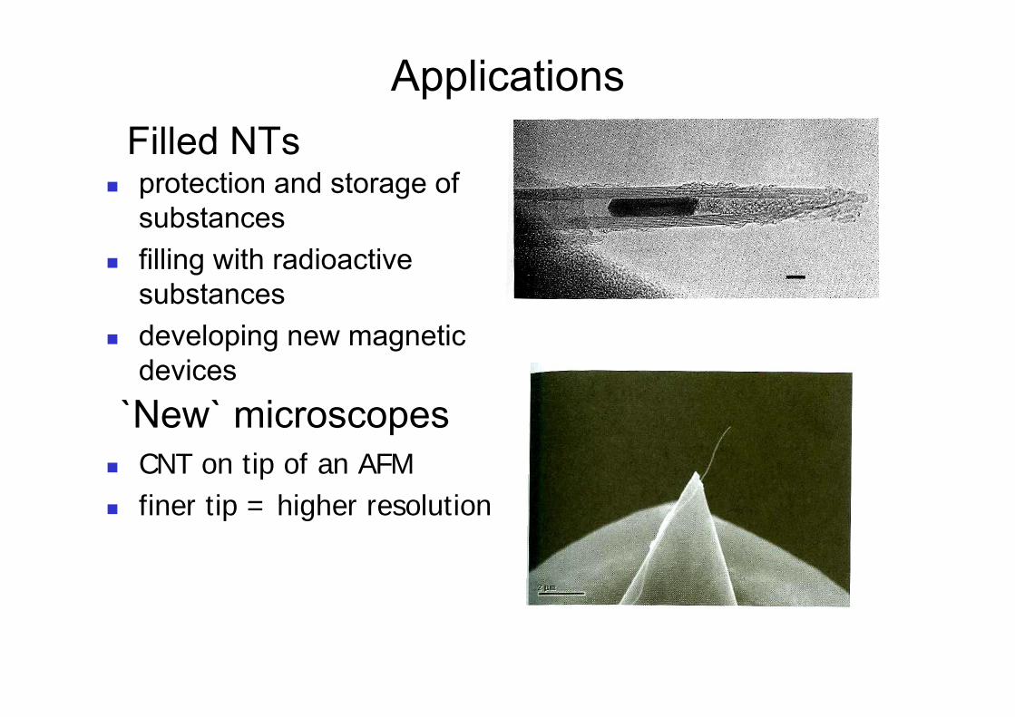
Applications
protection and storage of substancesfilling with radioactivesubstancesdeveloping new magneticdevices
Filled NTs
`New` microscopesCNT on tip of an AFMfiner tip = higher resolution
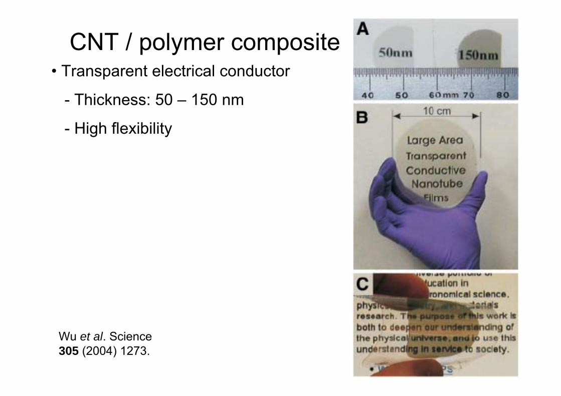
CNT / polymer composite
Wu et al. Science305 (2004) 1273.
• Transparent electrical conductor
- Thickness: 50 – 150 nm
- High flexibility
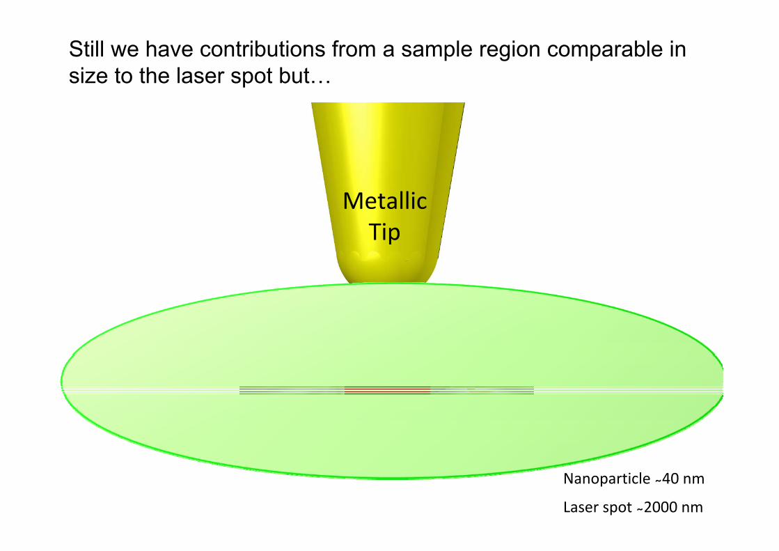
Laser spot ̴ 2000 nm Nanoparticle ̴ 40 nm
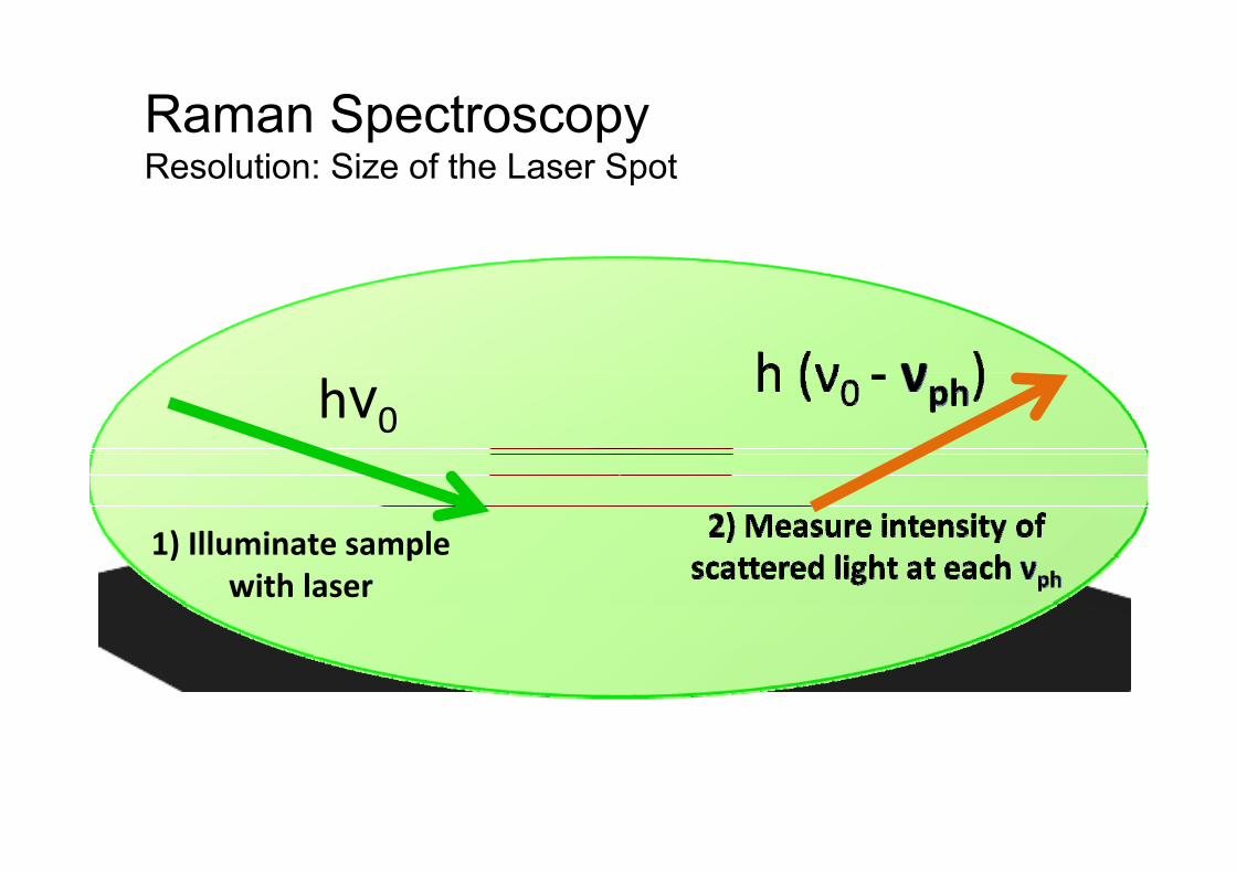
hν0
1) Illuminate sample with laser
Raman SpectroscopyResolution: Size of the Laser Spot
Metallic Tip
Still we have contributions from a sample region comparable in size to the laser spot but…
Laser spot ̴ 2000 nm
Nanoparticle ̴ 40 nm
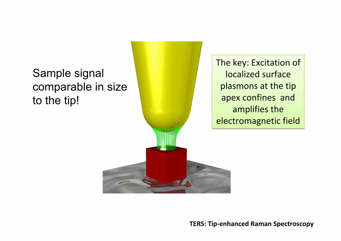
Sample signal comparable in size to the tip!
This is TERS
TERS: Tip‐enhanced Raman Spectroscopy
The key: Excitation of localized surface
plasmons at the tip apex confines and
amplifies the electromagnetic field
The key: Excitation of localized surface
plasmons at the tip apex confines and
amplifies the electromagnetic field
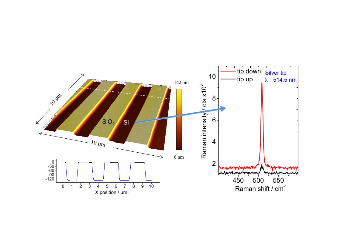
10 µm
10 µm
0 nm
SiSiO2
X position / μm
142 nm
0 1 2 3 4 5 6 7 8 9 10-120-90-60-30
0
Hei
ght
/ nm
450 500 550
2
4
6
8
10
Ram
an in
tens
ity /
cts
x103
Raman shift / cm-1
tip down tip up
Silver tipλ = 514.5 nm
AFM & Tip-Enhanced Raman Spectroscopy
E=2.7·107
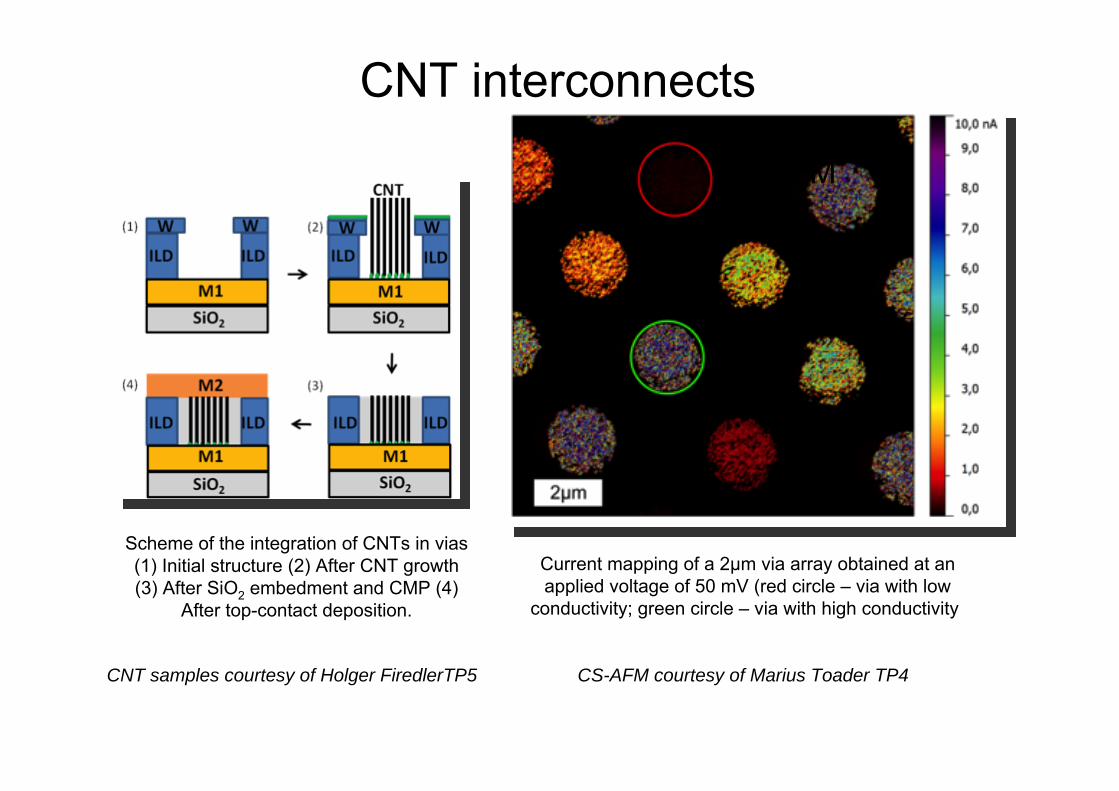
Scheme of the integration of CNTs in vias(1) Initial structure (2) After CNT growth (3) After SiO2 embedment and CMP (4)
After top-contact deposition.
Current mapping of a 2µm via array obtained at an applied voltage of 50 mV (red circle – via with low
conductivity; green circle – via with high conductivity)
CS-AFM
CS-AFM courtesy of Marius Toader TP4
CNT interconnects
CNT samples courtesy of Holger FiredlerTP5
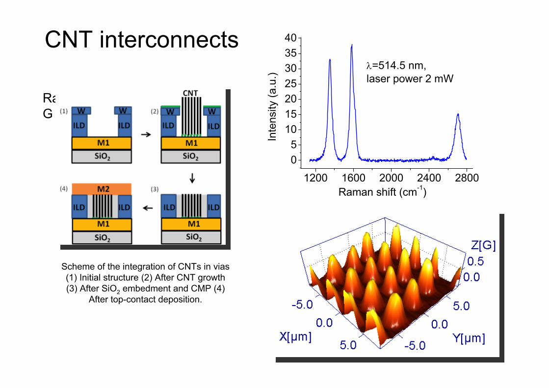
1200 1600 2000 2400 280005
10152025303540
Inte
nsity
(a.u
.)
Raman shift (cm-1)
λ=514.5 nm, laser power 2 mW
DG
2DRaman mapG band
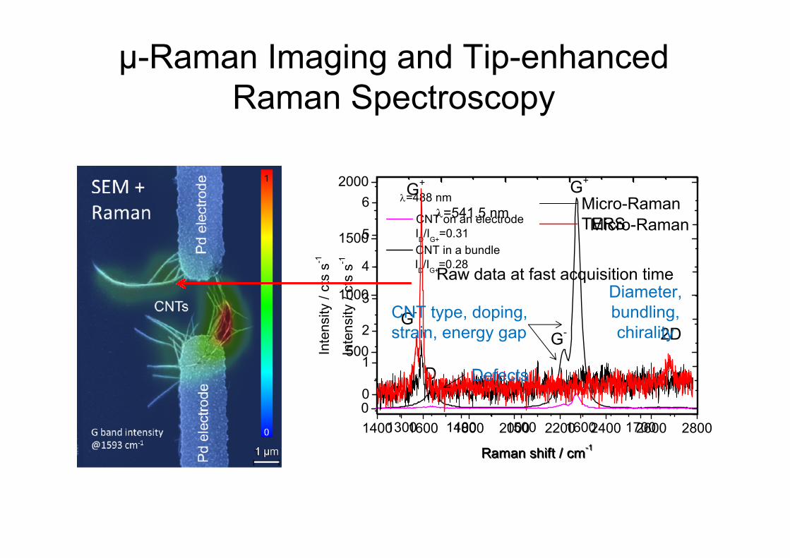
CNT interconnects
Scheme of the integration of CNTs in vias(1) Initial structure (2) After CNT growth (3) After SiO2 embedment and CMP (4)
After top-contact deposition.
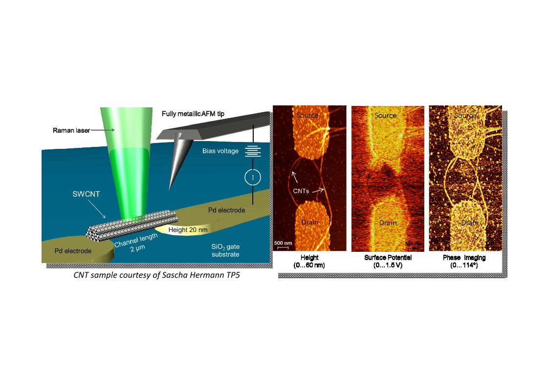
CNT sample courtesy of Sascha Hermann TP5
CNT FET
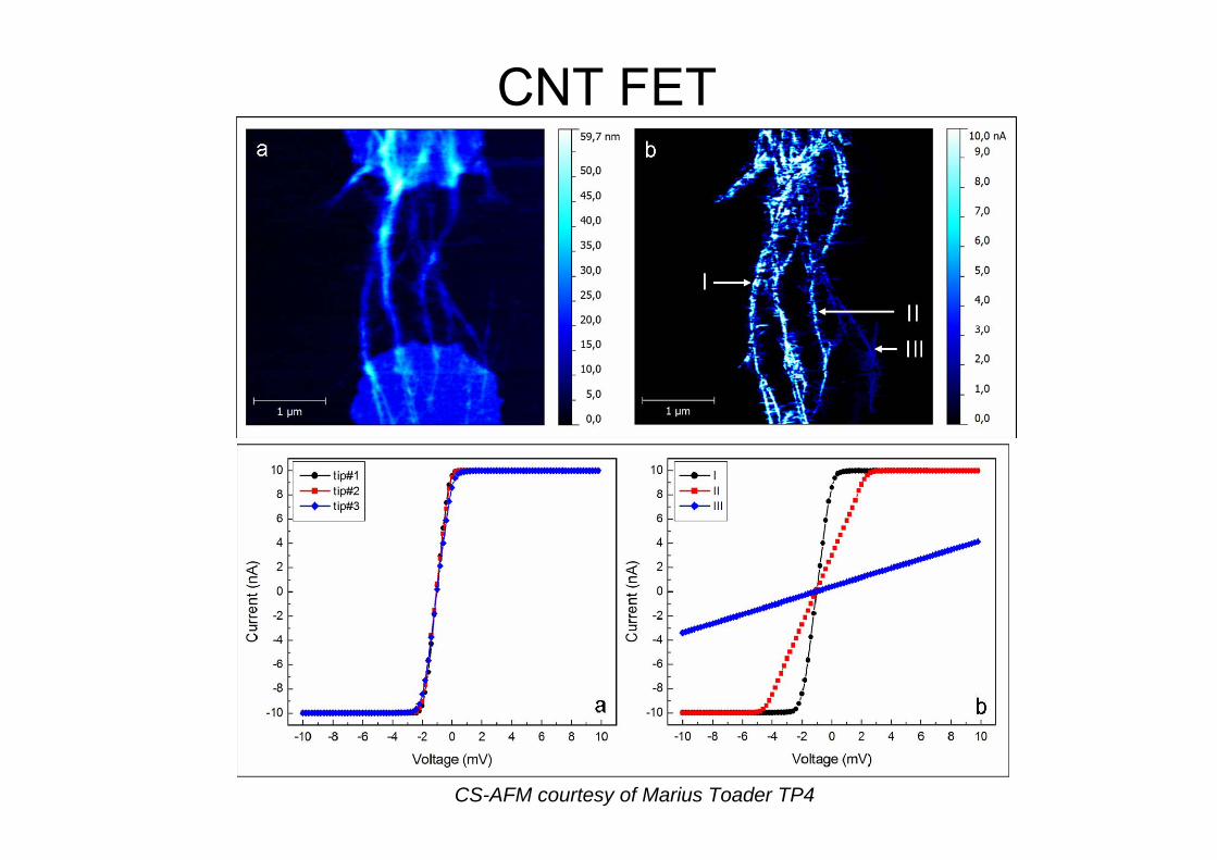
CS-AFM courtesy of Marius Toader TP4
CNT FET
1300 1400 1500 1600 17000
500
1000
1500
2000
CNT in a bundle ID/IG+=0.28
λ=488 nm
Inte
nsity
/ ct
s s-1
Raman shift / cm-1
D
G-
G+
CNT on an electrode ID/IG+=0.31 Micro-Raman
1400 1600 1800 2000 2200 2400 2600 2800
0
1
2
3
4
5
6 Micro-Raman TERS
λ=541.5 nm
Inte
nsity
/ ct
s s-1
Raman shift / cm-1
2DG-
G+
Raw data at fast acquisition time
Defects
CNT type, doping, strain, energy gap
Diameter, bundling, chirality
µ-Raman Imaging and Tip-enhanced Raman Spectroscopy
Challenges and future
Future applications:1. Already in product: CNT tipped AFM2. Big hit: CNT field effect transistors based nano electronics.3. Futuristic: CNT based OLED, artificial muscles…
Challenges1. Manufacture: Important parameters are hard to control.2. Large quantity fabrication process still missing.3. Manipulation of nanotubes.
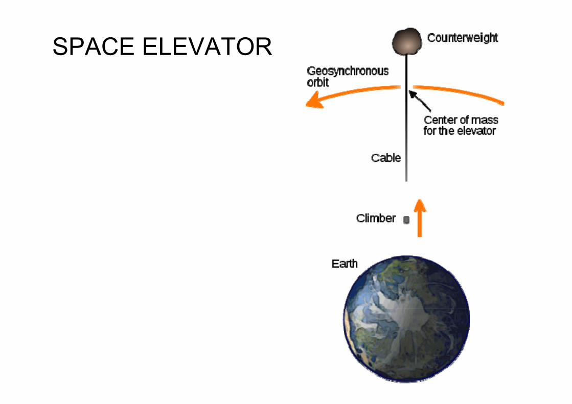
SPACE ELEVATOR
Semiconductor Physics Group Semiconductor Physics Group Chemnitz University of TechnologyChemnitz University of Technology