Embed Size (px)
Citation preview
SLUS492D − JUNE 2001 − REVISED SEPTEMBER 2007
1www.ti.com
FEATURES Industry-Standard Pin-Out
High Current Drive Capability of ±4 A at theMiller Plateau Region
Efficient Constant Current Sourcing Even atLow Supply Voltages
TTL/CMOS Compatible Inputs Independentof Supply Voltage
20-ns Typical Rise and 15-ns Typical FallTimes with 1.8-nF Load
Typical Propagation Delay Times of 25 nswith Input Falling and 35 ns with Input Rising
4-V to 15-V Supply Voltage
Supply Current of 0.3 mA
Dual Outputs Can Be Paralleled for HigherDrive Current
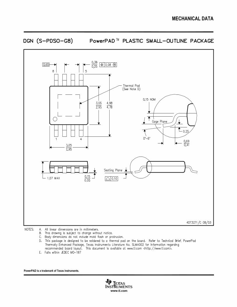
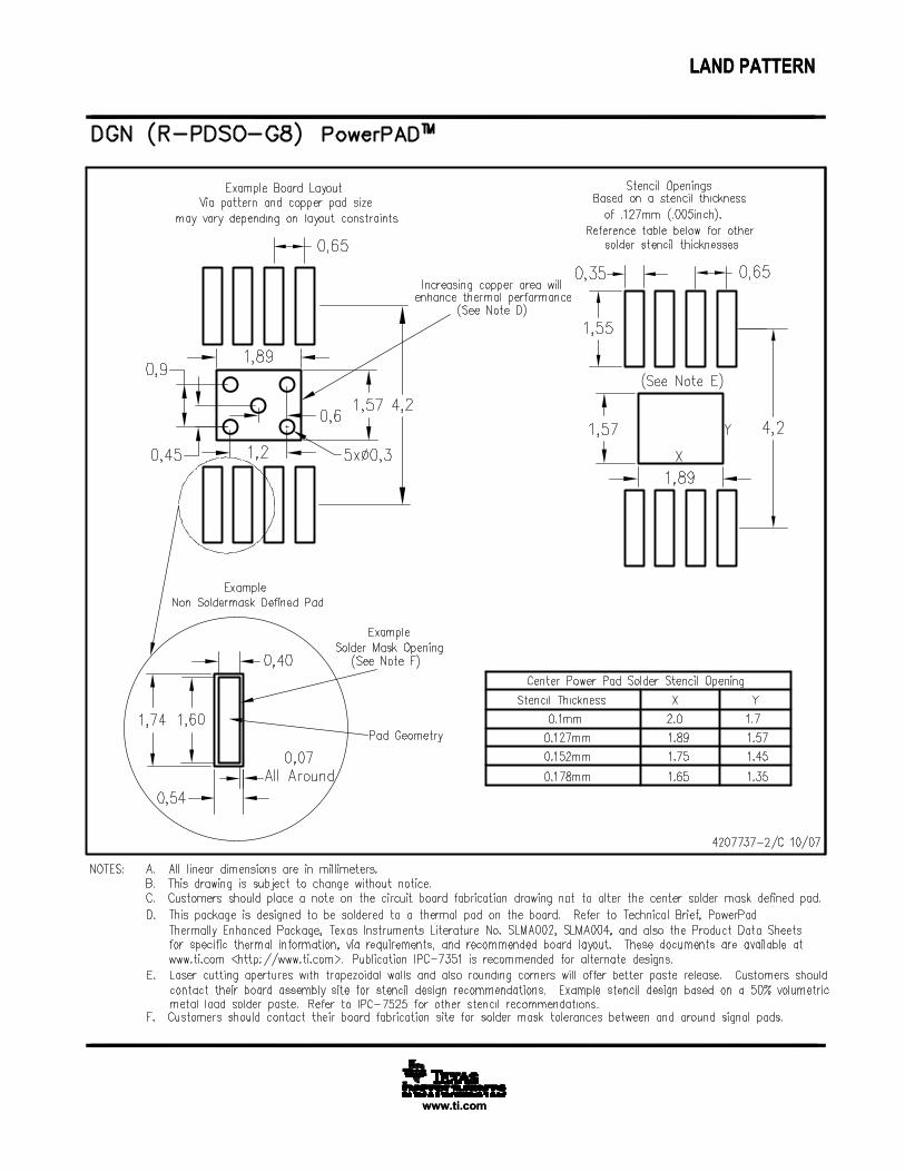
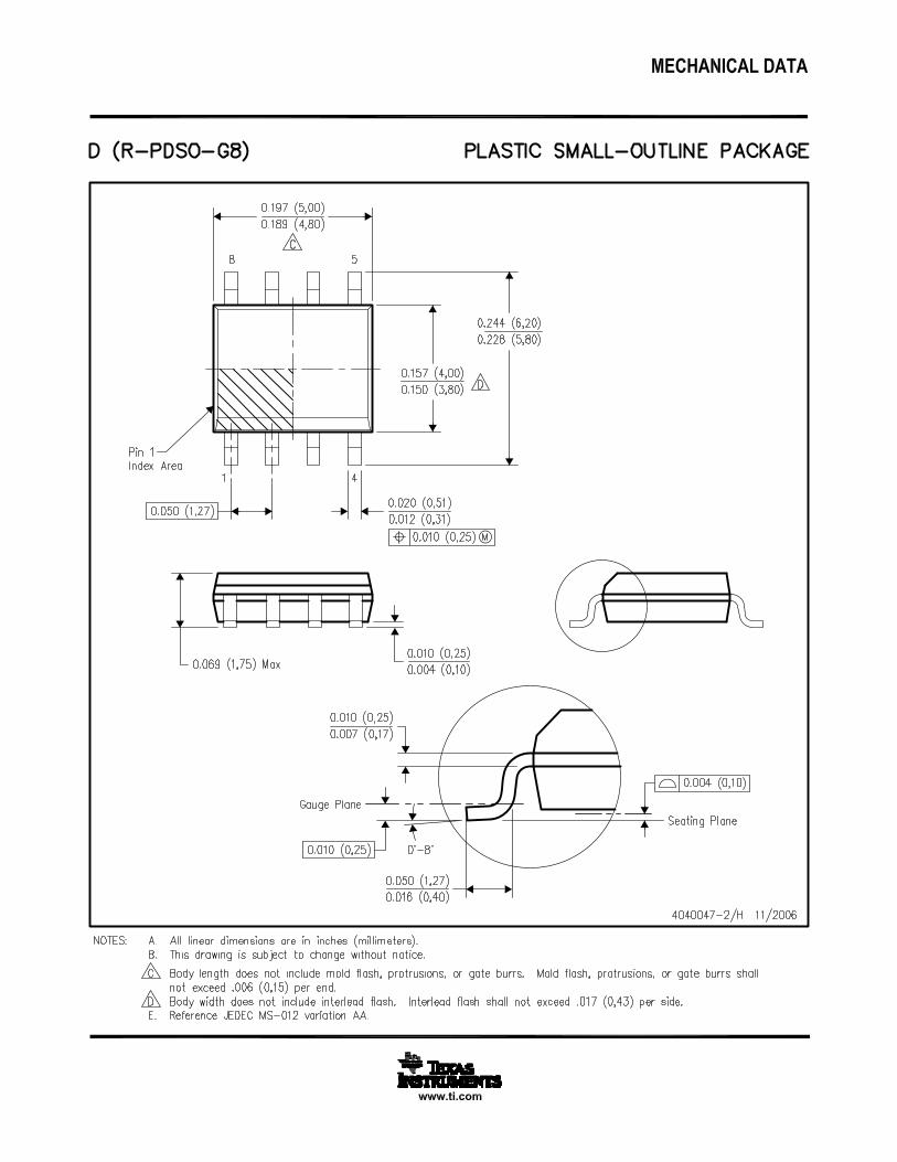
Available in Thermally Enhanced MSOPPowerPAD TM Package with 4.7 °C/W θjc
Rated From –40 °C to 85°C TrueDrive Output Architecture Using Bipolar
and CMOS Transistors in Parallel
APPLICATIONS Switch Mode Power Supplies
DC/DC Converters
Motor Controllers
Line Drivers
Class D Switching Amplifiers
DESCRIPTION
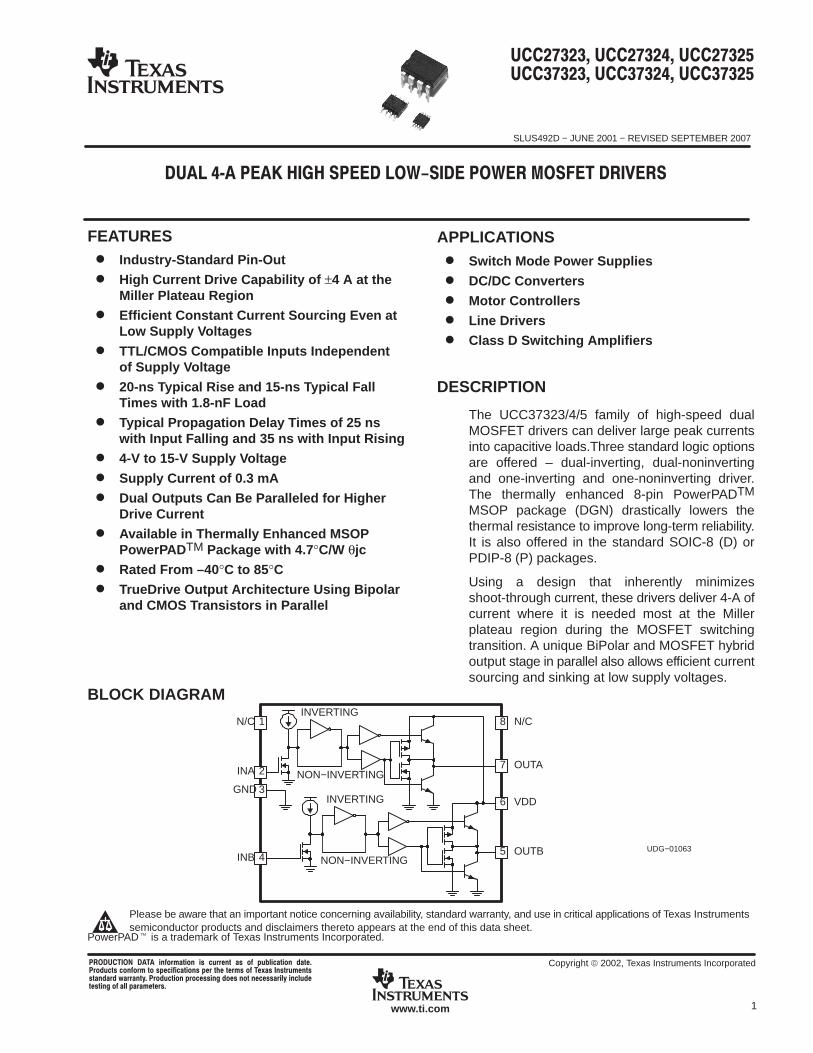
The UCC37323/4/5 family of high-speed dualMOSFET drivers can deliver large peak currentsinto capacitive loads.Three standard logic optionsare offered – dual-inverting, dual-noninvertingand one-inverting and one-noninverting driver.The thermally enhanced 8-pin PowerPADTM
MSOP package (DGN) drastically lowers thethermal resistance to improve long-term reliability.It is also offered in the standard SOIC-8 (D) orPDIP-8 (P) packages.
Using a design that inherently minimizesshoot-through current, these drivers deliver 4-A ofcurrent where it is needed most at the Millerplateau region during the MOSFET switchingtransition. A unique BiPolar and MOSFET hybridoutput stage in parallel also allows efficient currentsourcing and sinking at low supply voltages.
BLOCK DIAGRAM
1
OUTA
N/C
2INA
3GND
7
N/C8INVERTING
NON−INVERTING
OUTB4
5
INVERTING
NON−INVERTINGINB
6 VDD
UDG−01063
PowerPAD is a trademark of Texas Instruments Incorporated.
!"#$%! & '("")% $& ! *(+,'$%! -$%). "!-('%& '!!"# %! &*)''$%!& *)" %/) %)"#& ! )0$& &%"(#)%&&%$-$"- 1$""$%2. "!-('%! *"!')&&3 -!)& !% )')&&$",2 ',(-)%)&%3 ! $,, *$"$#)%)"&.
Copyright 2002, Texas Instruments Incorporated
Please be aware that an important notice concerning availability, standard warranty, and use in critical applications of Texas Instrumentssemiconductor products and disclaimers thereto appears at the end of this data sheet.
SLUS492D − JUNE 2001 − REVISED SEPTEMBER 2007
2 www.ti.com
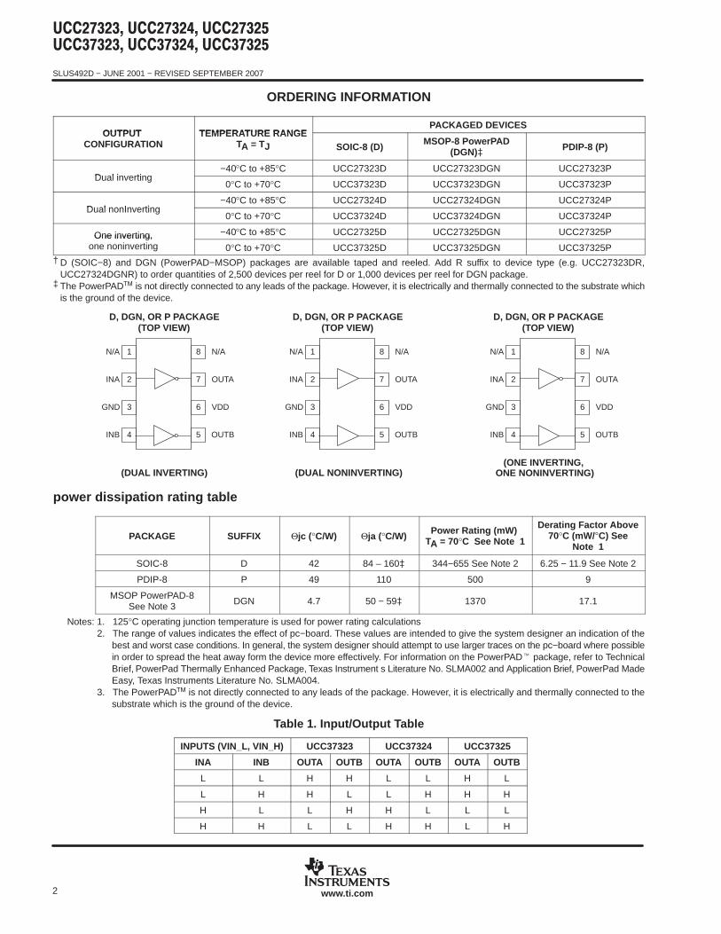
ORDERING INFORMATION
OUTPUT TEMPERATURE RANGEPACKAGED DEVICES
OUTPUT CONFIGURATION
TEMPERATURE RANGETA = TJ SOIC-8 (D)
MSOP-8 PowerPAD(DGN) PDIP-8 (P)
Dual inverting−40°C to +85°C UCC27323D UCC27323DGN UCC27323P
Dual inverting0°C to +70°C UCC37323D UCC37323DGN UCC37323P
Dual nonInverting−40°C to +85°C UCC27324D UCC27324DGN UCC27324P
Dual nonInverting0°C to +70°C UCC37324D UCC37324DGN UCC37324P
One inverting, −40°C to +85°C UCC27325D UCC27325DGN UCC27325POne inverting,one noninverting 0°C to +70°C UCC37325D UCC37325DGN UCC37325P
† D (SOIC−8) and DGN (PowerPAD−MSOP) packages are available taped and reeled. Add R suffix to device type (e.g. UCC27323DR,UCC27324DGNR) to order quantities of 2,500 devices per reel for D or 1,000 devices per reel for DGN package.
‡ The PowerPAD is not directly connected to any leads of the package. However, it is electrically and thermally connected to the substrate whichis the ground of the device.
D, DGN, OR P PACKAGE(TOP VIEW)
VDD
OUTA
N/A
OUTB
INA
N/A
GND
INB
1
2
3
4
8
7
6
5
D, DGN, OR P PACKAGE(TOP VIEW)
VDD
OUTA
N/A
OUTB
INA
N/A
GND
INB
1
2
3
4
8
7
6
5
D, DGN, OR P PACKAGE(TOP VIEW)
VDD
OUTA
N/A
OUTB
INA
N/A
GND
INB
1
2
3
4
8
7
6
5
(DUAL INVERTING) (DUAL NONINVERTING)(ONE INVERTING,
ONE NONINVERTING)
power dissipation rating table
PACKAGE SUFFIX Θjc (°C/W) Θja (°C/W)Power Rating (mW)
TA = 70°C See Note 1
Derating Factor Above70°C (mW/C) See
Note 1
SOIC-8 D 42 84 – 160 344−655 See Note 2 6.25 − 11.9 See Note 2
PDIP-8 P 49 110 500 9
MSOP PowerPAD-8See Note 3 DGN 4.7 50 − 59 1370 17.1
Notes: 1. 125°C operating junction temperature is used for power rating calculations2. The range of values indicates the effect of pc−board. These values are intended to give the system designer an indication of the
best and worst case conditions. In general, the system designer should attempt to use larger traces on the pc−board where possiblein order to spread the heat away form the device more effectively. For information on the PowerPAD package, refer to TechnicalBrief, PowerPad Thermally Enhanced Package, Texas Instrument s Literature No. SLMA002 and Application Brief, PowerPad MadeEasy, Texas Instruments Literature No. SLMA004.
3. The PowerPAD is not directly connected to any leads of the package. However, it is electrically and thermally connected to thesubstrate which is the ground of the device.
Table 1. Input/Output Table
INPUTS (VIN_L, VIN_H) UCC37323 UCC37324 UCC37325
INA INB OUTA OUTB OUTA OUTB OUTA OUTB
L L H H L L H L
L H H L L H H H
H L L H H L L L
H H L L H H L H
SLUS492D − JUNE 2001 − REVISED SEPTEMBER 2007
3www.ti.com
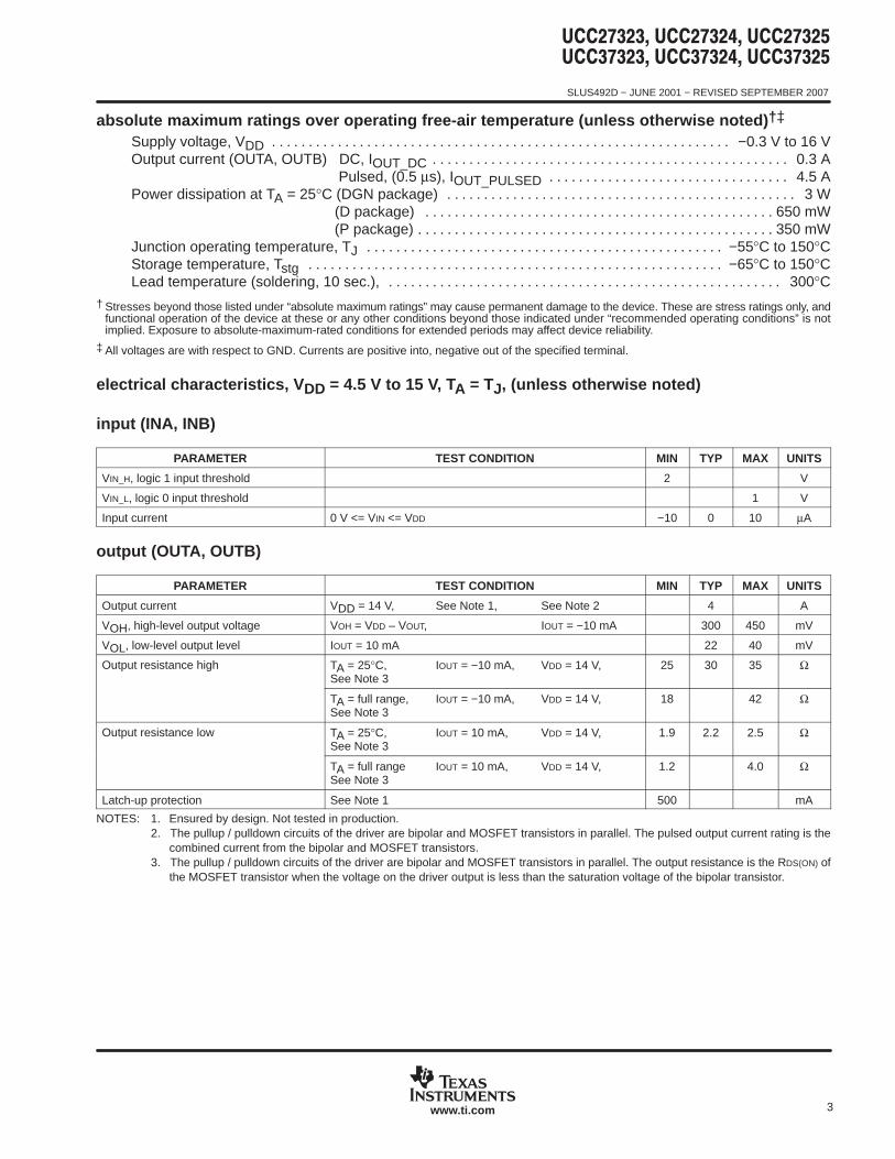
absolute maximum ratings over operating free-air temperature (unless otherwise noted) †
Supply voltage, VDD −0.3 V to 16 V. . . . . . . . . . . . . . . . . . . . . . . . . . . . . . . . . . . . . . . . . . . . . . . . . . . . . . . . . . . . . . . Output current (OUTA, OUTB) DC, IOUT_DC 0.3 A. . . . . . . . . . . . . . . . . . . . . . . . . . . . . . . . . . . . . . . . . . . . . . . . . Pulsed, (0.5 µs), IOUT_PULSED 4.5 A. . . . . . . . . . . . . . . . . . . . . . . . . . . . . . . . . Power dissipation at TA = 25°C (DGN package) 3 W. . . . . . . . . . . . . . . . . . . . . . . . . . . . . . . . . . . . . . . . . . . . . . . . (D package) 650 mW. . . . . . . . . . . . . . . . . . . . . . . . . . . . . . . . . . . . . . . . . . . . . . . . (P package) 350 mW. . . . . . . . . . . . . . . . . . . . . . . . . . . . . . . . . . . . . . . . . . . . . . . . . Junction operating temperature, TJ −55°C to 150°C. . . . . . . . . . . . . . . . . . . . . . . . . . . . . . . . . . . . . . . . . . . . . . . . . Storage temperature, Tstg −65°C to 150°C. . . . . . . . . . . . . . . . . . . . . . . . . . . . . . . . . . . . . . . . . . . . . . . . . . . . . . . . . Lead temperature (soldering, 10 sec.), 300°C. . . . . . . . . . . . . . . . . . . . . . . . . . . . . . . . . . . . . . . . . . . . . . . . . . . . . .
† Stresses beyond those listed under “absolute maximum ratings” may cause permanent damage to the device. These are stress ratings only, andfunctional operation of the device at these or any other conditions beyond those indicated under “recommended operating conditions” is notimplied. Exposure to absolute-maximum-rated conditions for extended periods may affect device reliability.
‡ All voltages are with respect to GND. Currents are positive into, negative out of the specified terminal.
electrical characteristics, V DD = 4.5 V to 15 V, TA = TJ, (unless otherwise noted)
input (INA, INB)
PARAMETER TEST CONDITION MIN TYP MAX UNITS
VIN_H, logic 1 input threshold 2 V
VIN_L, logic 0 input threshold 1 V
Input current 0 V <= VIN <= VDD −10 0 10 µA
output (OUTA, OUTB)
PARAMETER TEST CONDITION MIN TYP MAX UNITS
Output current VDD = 14 V, See Note 1, See Note 2 4 A
VOH, high-level output voltage VOH = VDD – VOUT, IOUT = −10 mA 300 450 mV
VOL, low-level output level IOUT = 10 mA 22 40 mV
Output resistance high TA = 25°C, IOUT = −10 mA, VDD = 14 V,See Note 3
25 30 35 Ω
TA = full range, IOUT = −10 mA, VDD = 14 V,See Note 3
18 42 Ω
Output resistance low TA = 25°C, IOUT = 10 mA, VDD = 14 V,See Note 3
1.9 2.2 2.5 Ω
TA = full range IOUT = 10 mA, VDD = 14 V,See Note 3
1.2 4.0 Ω
Latch-up protection See Note 1 500 mA
NOTES: 1. Ensured by design. Not tested in production.2. The pullup / pulldown circuits of the driver are bipolar and MOSFET transistors in parallel. The pulsed output current rating is the
combined current from the bipolar and MOSFET transistors.3. The pullup / pulldown circuits of the driver are bipolar and MOSFET transistors in parallel. The output resistance is the RDS(ON) of
the MOSFET transistor when the voltage on the driver output is less than the saturation voltage of the bipolar transistor.
SLUS492D − JUNE 2001 − REVISED SEPTEMBER 2007
4 www.ti.com
electrical characteristics, V DD = 4.5 V to 15 V, TA = −40C to 85C for the UCC2732x, T A = 0C to 70Cfor the UCC3732x, T A = TJ, (unless otherwise noted)
switching time
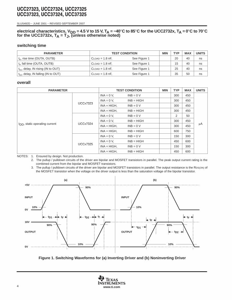
PARAMETER TEST CONDITION MIN TYP MAX UNITS
tR, rise time (OUTA, OUTB) CLOAD = 1.8 nF, See Figure 1 20 40 ns
tF, fall time (OUTA, OUTB) CLOAD = 1.8 nF, See Figure 1 15 40 ns
tD1, delay, IN rising (IN to OUT) CLOAD = 1.8 nF, See Figure 1 25 40 ns
tD2, delay, IN falling (IN to OUT) CLOAD = 1.8 nF, See Figure 1 35 50 ns
overall
PARAMETER TEST CONDITION MIN TYP MAX UNITS
INA = 0 V, INB = 0 V 300 450
UCCx7323INA = 0 V, INB = HIGH 300 450
UCCx7323INA = HIGH, INB = 0 V 300 450
INA = HIGH, INB = HIGH 300 450
INA = 0 V, INB = 0 V 2 50
IDD, static operating current UCCx7324INA = 0 V, INB = HIGH 300 450
AIDD, static operating current UCCx7324INA = HIGH, INB = 0 V 300 450
µA
INA = HIGH, INB = HIGH 600 750
INA = 0 V, INB = 0 V 150 300
UCCx7325INA = 0 V, INB = HIGH 450 600
UCCx7325INA = HIGH, INB = 0 V 150 300
INA = HIGH, INB = HIGH 450 600
NOTES: 1. Ensured by design. Not production.2. The pullup / pulldown circuits of the driver are bipolar and MOSFET transistors in parallel. The peak output current rating is the
combined current from the bipolar and MOSFET transistors.3. The pullup / pulldown circuits of the driver are bipolar and MOSFET transistors in parallel. The output resistance is the RDS(ON) of
the MOSFET transistor when the voltage on the driver output is less than the saturation voltage of the bipolar transistor.
+5V
INPUT
16V
OUTPUT
0V
0V
10%
90%
10%
90%
(a)
90%
90%
10%
90%
(b)
INPUT
OUTPUT
10%
tD1 tD2tF tf
tD1
tFtF
tD2
Figure 1. Switching Waveforms for (a) Inverting Driver and (b) Noninverting Driver
SLUS492D − JUNE 2001 − REVISED SEPTEMBER 2007
5www.ti.com
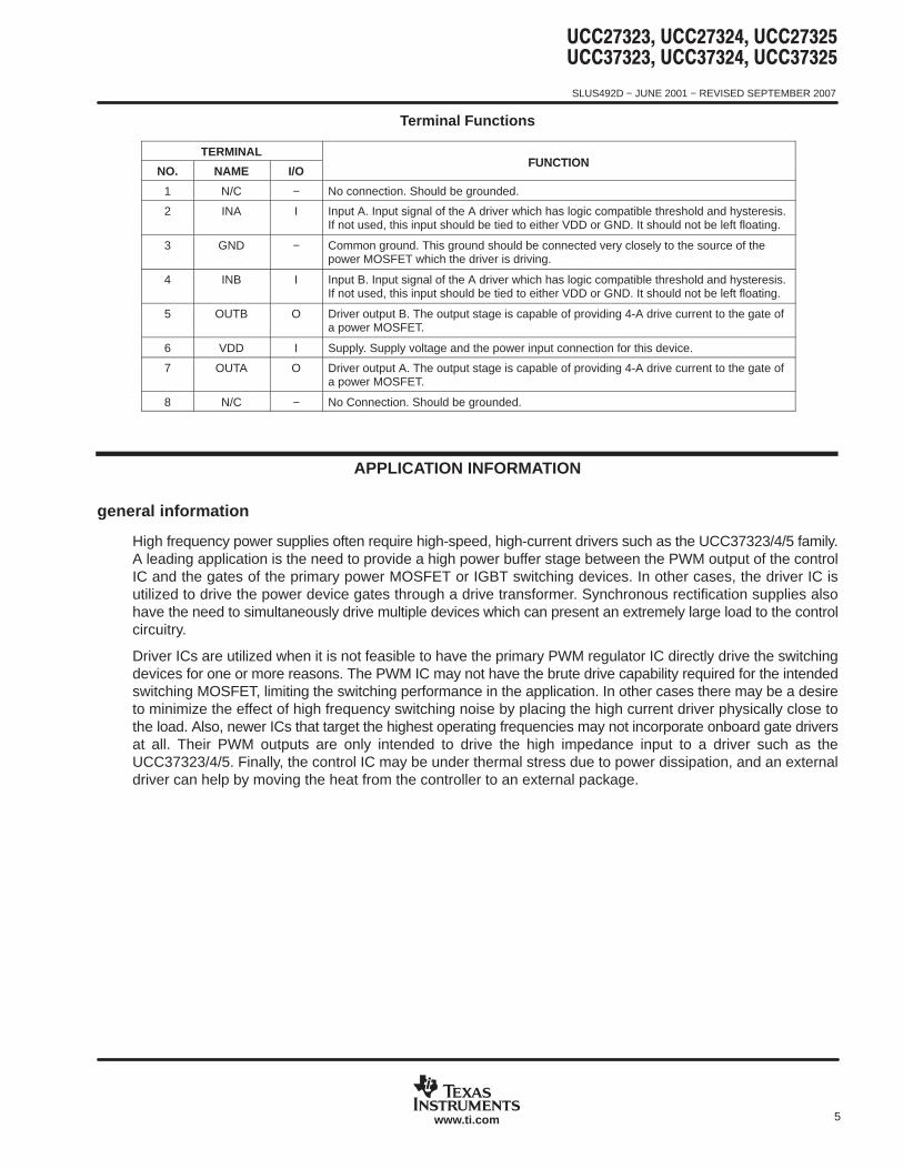
Terminal Functions
TERMINALFUNCTION
NO. NAME I/OFUNCTION
1 N/C − No connection. Should be grounded.
2 INA I Input A. Input signal of the A driver which has logic compatible threshold and hysteresis.If not used, this input should be tied to either VDD or GND. It should not be left floating.
3 GND − Common ground. This ground should be connected very closely to the source of thepower MOSFET which the driver is driving.
4 INB I Input B. Input signal of the A driver which has logic compatible threshold and hysteresis.If not used, this input should be tied to either VDD or GND. It should not be left floating.
5 OUTB O Driver output B. The output stage is capable of providing 4-A drive current to the gate ofa power MOSFET.
6 VDD I Supply. Supply voltage and the power input connection for this device.
7 OUTA O Driver output A. The output stage is capable of providing 4-A drive current to the gate ofa power MOSFET.
8 N/C − No Connection. Should be grounded.
APPLICATION INFORMATION
general information
High frequency power supplies often require high-speed, high-current drivers such as the UCC37323/4/5 family.A leading application is the need to provide a high power buffer stage between the PWM output of the controlIC and the gates of the primary power MOSFET or IGBT switching devices. In other cases, the driver IC isutilized to drive the power device gates through a drive transformer. Synchronous rectification supplies alsohave the need to simultaneously drive multiple devices which can present an extremely large load to the controlcircuitry.
Driver ICs are utilized when it is not feasible to have the primary PWM regulator IC directly drive the switchingdevices for one or more reasons. The PWM IC may not have the brute drive capability required for the intendedswitching MOSFET, limiting the switching performance in the application. In other cases there may be a desireto minimize the effect of high frequency switching noise by placing the high current driver physically close tothe load. Also, newer ICs that target the highest operating frequencies may not incorporate onboard gate driversat all. Their PWM outputs are only intended to drive the high impedance input to a driver such as theUCC37323/4/5. Finally, the control IC may be under thermal stress due to power dissipation, and an externaldriver can help by moving the heat from the controller to an external package.
SLUS492D − JUNE 2001 − REVISED SEPTEMBER 2007
6 www.ti.com
APPLICATION INFORMATION
input stage
The input thresholds have a 3.3−V logic sensitivity over the full range of VDD voltage; yet it is equally compatablewith 0 V to VDD signals.
The inputs of UCC37323/4/5 family of drivers are designed to withstand 500-mA reverse current without eitherdamage to the IC for logic upset. The input stage of each driver should be driven by a signal with a short riseor fall time. This condition is satisfied in typical power supply applications, where the input signals are providedby a PWM controller or logic gates with fast transition times (<200 ns). The input stages to the drivers functionas a digital gate, and they are not intended for applications where a slow changing input voltage is used togenerate a switching output when the logic threshold of the input section is reached. While this may not beharmful to the driver, the output of the driver may switch repeatedly at a high frequency.
Users should not attempt to shape the input signals to the driver in an attempt to slow down (or delay) the signalat the output. If limiting the rise or fall times to the power device is desired, limit the rise or fall times to the powerdevice, then an external resistance can be added between the output of the driver and the load device, whichis generally a power MOSFET gate. The external resistor may also help remove power dissipation from the ICpackage, as discussed in the section on Thermal Considerations.
output stage
Inverting outputs of the UCC37323 and OUTA of the UCC37325 are intended to drive external P-channelMOSFETs. Noninverting outputs of the UCC37324 and OUTB of the UCC37325 are intended to drive externalN-channel MOSFETs.
Each output stage is capable of supplying ±4-A peak current pulses and swings to both VDD and GND. Thepullup/ pulldown circuits of the driver are constructed of bipolar and MOSFET transistors in parallel. The peakoutput current rating is the combined current from the bipolar and MOSFET transistors. The output resistanceis the RDS(on) of the MOSFET transistor when the voltage on the driver output is less than the saturation voltageof the bipolar transistor. Each output stage also provides a very low impedance to overshoot and undershootdue to the body diode of the internal MOSFET. This means that in many cases, external-schottky-clamp diodesare not required.
The UCC37323 family delivers 4-A of gate drive where it is most needed during the MOSFET switchingtransition – at the Miller plateau region – providing improved efficiency gains. A unique BiPolar and MOSFEThybrid output stage in parallel also allows efficient current sourcing at low supply voltages.
SLUS492D − JUNE 2001 − REVISED SEPTEMBER 2007
7www.ti.com
APPLICATION INFORMATION
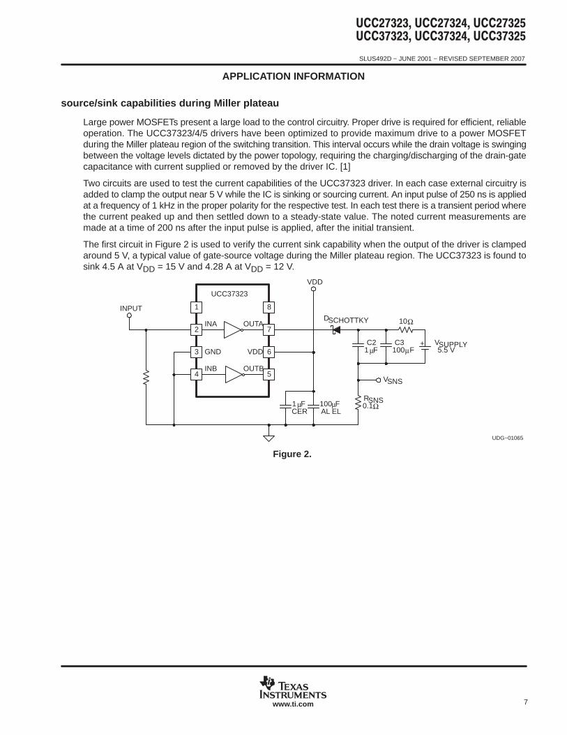
source/sink capabilities during Miller plateau
Large power MOSFETs present a large load to the control circuitry. Proper drive is required for efficient, reliableoperation. The UCC37323/4/5 drivers have been optimized to provide maximum drive to a power MOSFETduring the Miller plateau region of the switching transition. This interval occurs while the drain voltage is swingingbetween the voltage levels dictated by the power topology, requiring the charging/discharging of the drain-gatecapacitance with current supplied or removed by the driver IC. [1]
Two circuits are used to test the current capabilities of the UCC37323 driver. In each case external circuitry isadded to clamp the output near 5 V while the IC is sinking or sourcing current. An input pulse of 250 ns is appliedat a frequency of 1 kHz in the proper polarity for the respective test. In each test there is a transient period wherethe current peaked up and then settled down to a steady-state value. The noted current measurements aremade at a time of 200 ns after the input pulse is applied, after the initial transient.
The first circuit in Figure 2 is used to verify the current sink capability when the output of the driver is clampedaround 5 V, a typical value of gate-source voltage during the Miller plateau region. The UCC37323 is found tosink 4.5 A at VDD = 15 V and 4.28 A at VDD = 12 V.
UDG−01065
UCC37323
GND
1
2
3
4INB
INA7
6
5
8
OUTA
VDD
OUTB
INPUT
1 µFCER
100µFAL EL
DSCHOTTKY
VDD
C21 µF
VSNS
RSNS0.1Ω
C3100µF
10Ω
+ VSUPPLY5.5 V
Figure 2.
SLUS492D − JUNE 2001 − REVISED SEPTEMBER 2007
8 www.ti.com
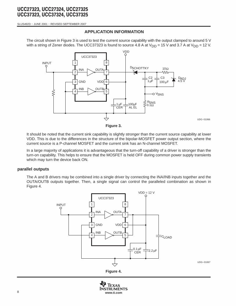
APPLICATION INFORMATION
The circuit shown in Figure 3 is used to test the current source capability with the output clamped to around 5 Vwith a string of Zener diodes. The UCC37323 is found to source 4.8 A at VDD = 15 V and 3.7 A at VDD = 12 V.
UCC37323
GND
1
2
3
4INB
INA7
6
5
8
OUTA
VDD
OUTB
INPUT
1 µFCER
100µFAL EL
DSCHOTTKY
VDD
C21 µF
VSNS
RSNS0.1Ω
C3100 µF
10Ω
DADJ4.5 V
UDG−01066
Figure 3.
It should be noted that the current sink capability is slightly stronger than the current source capability at lowerVDD. This is due to the differences in the structure of the bipolar-MOSFET power output section, where thecurrent source is a P-channel MOSFET and the current sink has an N-channel MOSFET.
In a large majority of applications it is advantageous that the turn-off capability of a driver is stronger than theturn-on capability. This helps to ensure that the MOSFET is held OFF during common power supply transientswhich may turn the device back ON.
parallel outputs
The A and B drivers may be combined into a single driver by connecting the INA/INB inputs together and theOUTA/OUTB outputs together. Then, a single signal can control the paralleled combination as shown inFigure 4.
UDG−01067
UCC37323
GND
1
2
3
4INB
INA7
6
5
8
OUTA
VDD
OUTB
INPUT
0.1 µFCER 2.2 µF
VDD = 12 V
CLOAD
Figure 4.
SLUS492D − JUNE 2001 − REVISED SEPTEMBER 2007
9www.ti.com
APPLICATION INFORMATION
operational waveforms and circuit layout
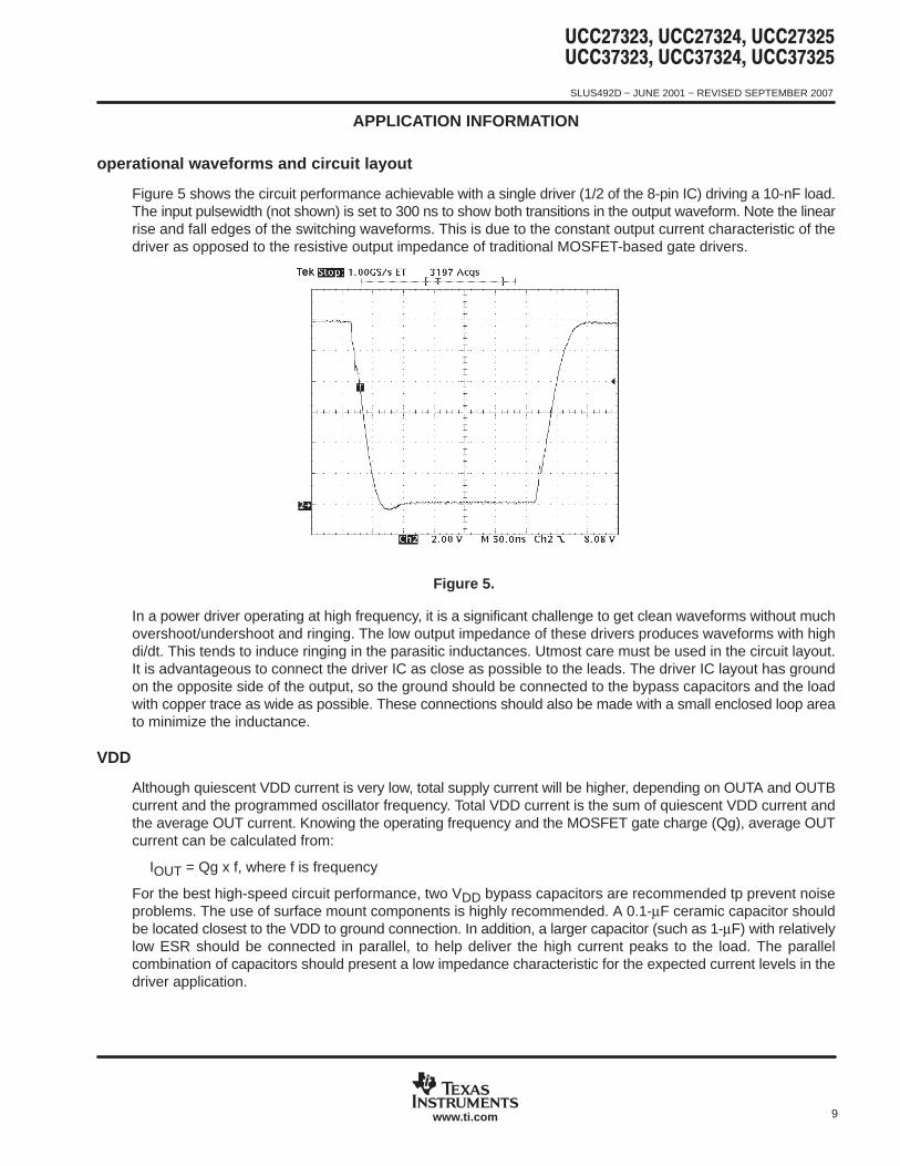
Figure 5 shows the circuit performance achievable with a single driver (1/2 of the 8-pin IC) driving a 10-nF load.The input pulsewidth (not shown) is set to 300 ns to show both transitions in the output waveform. Note the linearrise and fall edges of the switching waveforms. This is due to the constant output current characteristic of thedriver as opposed to the resistive output impedance of traditional MOSFET-based gate drivers.
Figure 5.
In a power driver operating at high frequency, it is a significant challenge to get clean waveforms without muchovershoot/undershoot and ringing. The low output impedance of these drivers produces waveforms with highdi/dt. This tends to induce ringing in the parasitic inductances. Utmost care must be used in the circuit layout.It is advantageous to connect the driver IC as close as possible to the leads. The driver IC layout has groundon the opposite side of the output, so the ground should be connected to the bypass capacitors and the loadwith copper trace as wide as possible. These connections should also be made with a small enclosed loop areato minimize the inductance.
VDD
Although quiescent VDD current is very low, total supply current will be higher, depending on OUTA and OUTBcurrent and the programmed oscillator frequency. Total VDD current is the sum of quiescent VDD current andthe average OUT current. Knowing the operating frequency and the MOSFET gate charge (Qg), average OUTcurrent can be calculated from:
IOUT = Qg x f, where f is frequency
For the best high-speed circuit performance, two VDD bypass capacitors are recommended tp prevent noiseproblems. The use of surface mount components is highly recommended. A 0.1-µF ceramic capacitor shouldbe located closest to the VDD to ground connection. In addition, a larger capacitor (such as 1-µF) with relativelylow ESR should be connected in parallel, to help deliver the high current peaks to the load. The parallelcombination of capacitors should present a low impedance characteristic for the expected current levels in thedriver application.
SLUS492D − JUNE 2001 − REVISED SEPTEMBER 2007
10 www.ti.com
APPLICATION INFORMATION
drive current and power requirements
The UCC37323/4/5 family of drivers are capable of delivering 4-A of current to a MOSFET gate for a period ofseveral hundred nanoseconds. High peak current is required to turn the device ON quickly. Then, to turn thedevice OFF, the driver is required to sink a similar amount of current to ground. This repeats at the operatingfrequency of the power device. A MOSFET is used in this discussion because it is the most common type ofswitching device used in high frequency power conversion equipment.
References 1 and 2 discuss the current required to drive a power MOSFET and other capacitive-input switchingdevices. Reference 2 includes information on the previous generation of bipolar IC gate drivers.
When a driver IC is tested with a discrete, capacitive load it is a fairly simple matter to calculate the power thatis required from the bias supply. The energy that must be transferred from the bias supply to charge the capacitoris given by:
E 12
CV2, where C is the load capacitor and V is the bias voltage feeding the driver.
There is an equal amount of energy transferred to ground when the capacitor is discharged. This leads to apower loss given by the following:
P 2 12
CV2f, where f is the switching frequency.
This power is dissipated in the resistive elements of the circuit. Thus, with no external resistor between the driverand gate, this power is dissipated inside the driver. Half of the total power is dissipated when the capacitor ischarged, and the other half is dissipated when the capacitor is discharged. An actual example using theconditions of the previous gate drive waveform should help clarify this.
With VDD = 12 V, CLOAD = 10 nF, and f = 300 kHz, the power loss can be calculated as:
P = 10 nF x (12)2 x (300 kHz) = 0.432 W
With a 12-V supply, this would equate to a current of:
I PV
0.432 W12 V
0.036 A
The actual current measured from the supply was 0.037 A, and is very close to the predicted value. But, theIDD current that is due to the IC internal consumption should be considered. With no load the IC current drawis 0.0027 A. Under this condition the output rise and fall times are faster than with a load. This could lead to analmost insignificant, yet measurable current due to cross-conduction in the output stages of the driver. However,these small current differences are buried in the high frequency switching spikes, and are beyond themeasurement capabilities of a basic lab setup. The measured current with 10-nF load is reasonably close tothat expected.
SLUS492D − JUNE 2001 − REVISED SEPTEMBER 2007
11www.ti.com
APPLICATION INFORMATION
The switching load presented by a power MOSFET can be converted to an equivalent capacitance by examiningthe gate charge required to switch the device. This gate charge includes the effects of the input capacitanceplus the added charge needed to swing the drain of the device between the ON and OFF states. Mostmanufacturers provide specifications that provide the typical and maximum gate charge, in nC, to switch thedevice under specified conditions. Using the gate charge Qg, one can determine the power that must bedissipated when charging a capacitor. This is done by using the equivalence Qg = CeffV to provide the followingequation for power:
P C V2 f Qg f
This equation allows a power designer to calculate the bias power required to drive a specific MOSFET gateat a specific bias voltage.
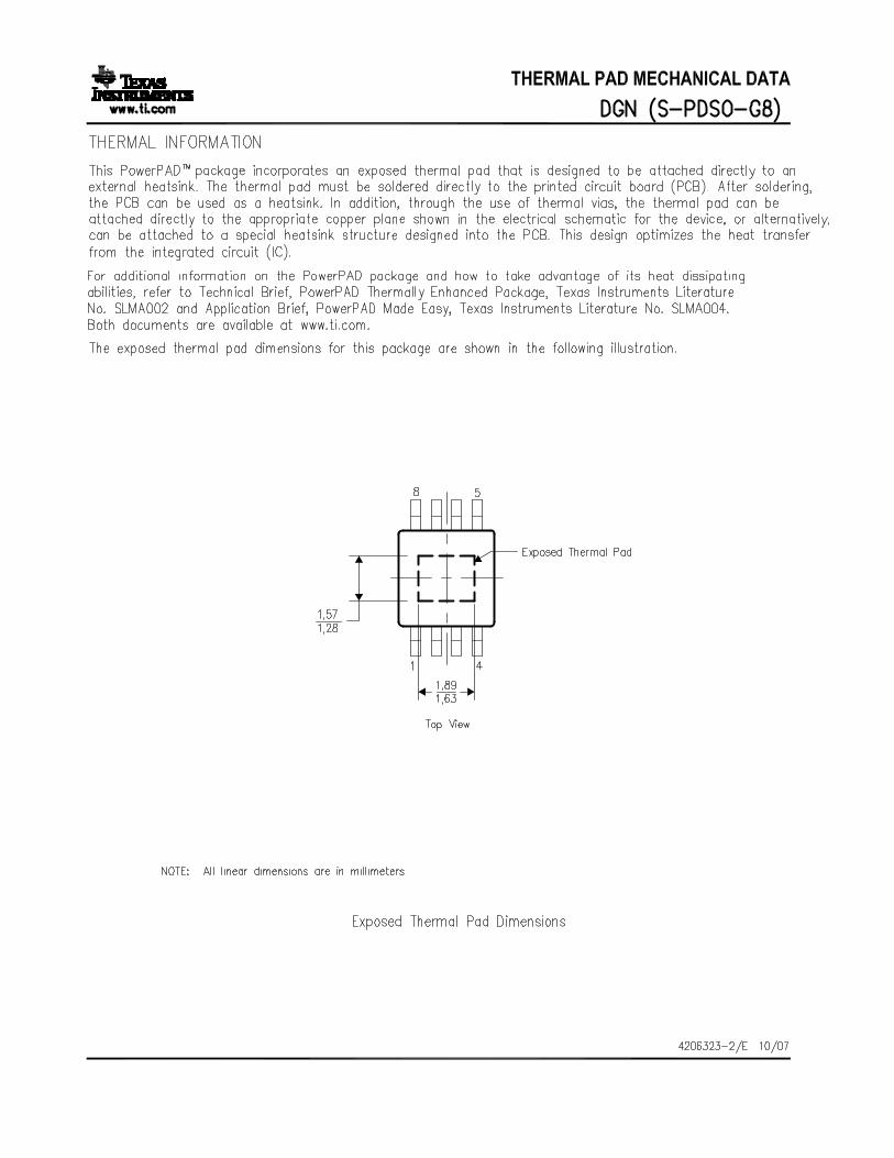
THERMAL INFORMATION
The useful range of a driver is greatly affected by the drive power requirements of the load and the thermalcharacteristics of the IC package. In order for a power driver to be useful over a particular temperature rangethe package must allow for the efficient removal of the heat produced while keeping the junction temperaturewithin rated limits. The UCC37323/4/5 family of drivers is available in three different packages to cover a rangeof application requirements.
As shown in the power dissipation rating table, the SOIC-8 (D) and PDIP-8 (P) packages each have a powerrating of around 0.5 W with TA = 70°C. This limit is imposed in conjunction with the power derating factor alsogiven in the table. Note that the power dissipation in our earlier example is 0.432 W with a 10-nF load, 12 VDD,switched at 300 kHz. Thus, only one load of this size could be driven using the D or P package, even if the twoonboard drivers are paralleled. The difficulties with heat removal limit the drive available in the older packages.
The MSOP PowerPAD-8 (DGN) package significantly relieves this concern by offering an effective means ofremoving the heat from the semiconductor junction. As illustrated in Reference 3, the PowerPAD packages offera leadframe die pad that is exposed at the base of the package. This pad is soldered to the copper on the PCboard directly underneath the IC package, reducing the Θjc down to 4.7°C/W. Data is presented in Reference 3to show that the power dissipation can be quadrupled in the PowerPAD configuration when compared to thestandard packages. The PC board must be designed with thermal lands and thermal vias to complete the heatremoval subsystem, as summarized in Reference 4. This allows a significant improvement in heatsinking overthat available in the D or P packages, and is shown to more than double the power capability of the D and Ppackages.
NOTE:The PowerPAD is not directly connected to any leads of the package. However, it iselectrically and thermally connected to the substrate which is the ground of the device.
references
1. Power Supply Seminar SEM−1400 Topic 2: Design And Application Guide For High Speed MOSFETGate Drive Circuits, by Laszlo Balogh, Texas Instruments Literature No. SLUP133.
2. Application Note, Practical Considerations in High Performance MOSFET, IGBT and MCT Gate DriveCircuits, by Bill Andreycak, Texas Instruments Literature No. SLUA105
3. Technical Brief, PowerPad Thermally Enhanced Package, Texas Instruments Literature No. SLMA002
4. Application Brief, PowerPAD Made Easy, Texas Instruments Literature No. SLMA004
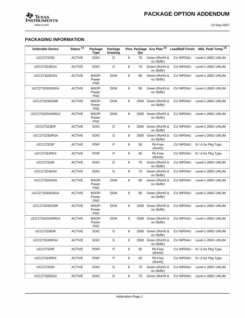
PACKAGING INFORMATION
Orderable Device Status (1) PackageType
PackageDrawing
Pins PackageQty
Eco Plan (2) Lead/Ball Finish MSL Peak Temp (3)
UCC27323D ACTIVE SOIC D 8 75 Green (RoHS &no Sb/Br)
CU NIPDAU Level-1-260C-UNLIM
UCC27323DG4 ACTIVE SOIC D 8 75 Green (RoHS &no Sb/Br)
CU NIPDAU Level-1-260C-UNLIM
UCC27323DGN ACTIVE MSOP-Power PAD
DGN 8 80 Green (RoHS &no Sb/Br)
CU NIPDAU Level-1-260C-UNLIM
UCC27323DGNG4 ACTIVE MSOP-Power PAD
DGN 8 80 Green (RoHS &no Sb/Br)
CU NIPDAU Level-1-260C-UNLIM
UCC27323DGNR ACTIVE MSOP-Power PAD
DGN 8 2500 Green (RoHS &no Sb/Br)
CU NIPDAU Level-1-260C-UNLIM
UCC27323DGNRG4 ACTIVE MSOP-Power PAD
DGN 8 2500 Green (RoHS &no Sb/Br)
CU NIPDAU Level-1-260C-UNLIM
UCC27323DR ACTIVE SOIC D 8 2500 Green (RoHS &no Sb/Br)
CU NIPDAU Level-1-260C-UNLIM
UCC27323DRG4 ACTIVE SOIC D 8 2500 Green (RoHS &no Sb/Br)
CU NIPDAU Level-1-260C-UNLIM
UCC27323P ACTIVE PDIP P 8 50 Pb-Free(RoHS)
CU NIPDAU N / A for Pkg Type
UCC27323PE4 ACTIVE PDIP P 8 50 Pb-Free(RoHS)
CU NIPDAU N / A for Pkg Type
UCC27324D ACTIVE SOIC D 8 75 Green (RoHS &no Sb/Br)
CU NIPDAU Level-1-260C-UNLIM
UCC27324DG4 ACTIVE SOIC D 8 75 Green (RoHS &no Sb/Br)
CU NIPDAU Level-1-260C-UNLIM
UCC27324DGN ACTIVE MSOP-Power PAD
DGN 8 80 Green (RoHS &no Sb/Br)
CU NIPDAU Level-1-260C-UNLIM
UCC27324DGNG4 ACTIVE MSOP-Power PAD
DGN 8 80 Green (RoHS &no Sb/Br)
CU NIPDAU Level-1-260C-UNLIM
UCC27324DGNR ACTIVE MSOP-Power PAD
DGN 8 2500 Green (RoHS &no Sb/Br)
CU NIPDAU Level-1-260C-UNLIM
UCC27324DGNRG4 ACTIVE MSOP-Power PAD
DGN 8 2500 Green (RoHS &no Sb/Br)
CU NIPDAU Level-1-260C-UNLIM
UCC27324DR ACTIVE SOIC D 8 2500 Green (RoHS &no Sb/Br)
CU NIPDAU Level-1-260C-UNLIM
UCC27324DRG4 ACTIVE SOIC D 8 2500 Green (RoHS &no Sb/Br)
CU NIPDAU Level-1-260C-UNLIM
UCC27324P ACTIVE PDIP P 8 50 Pb-Free(RoHS)
CU NIPDAU N / A for Pkg Type
UCC27324PE4 ACTIVE PDIP P 8 50 Pb-Free(RoHS)
CU NIPDAU N / A for Pkg Type
UCC27325D ACTIVE SOIC D 8 75 Green (RoHS &no Sb/Br)
CU NIPDAU Level-1-260C-UNLIM
UCC27325DG4 ACTIVE SOIC D 8 75 Green (RoHS & CU NIPDAU Level-1-260C-UNLIM
PACKAGE OPTION ADDENDUM
www.ti.com 13-Sep-2007
Addendum-Page 1
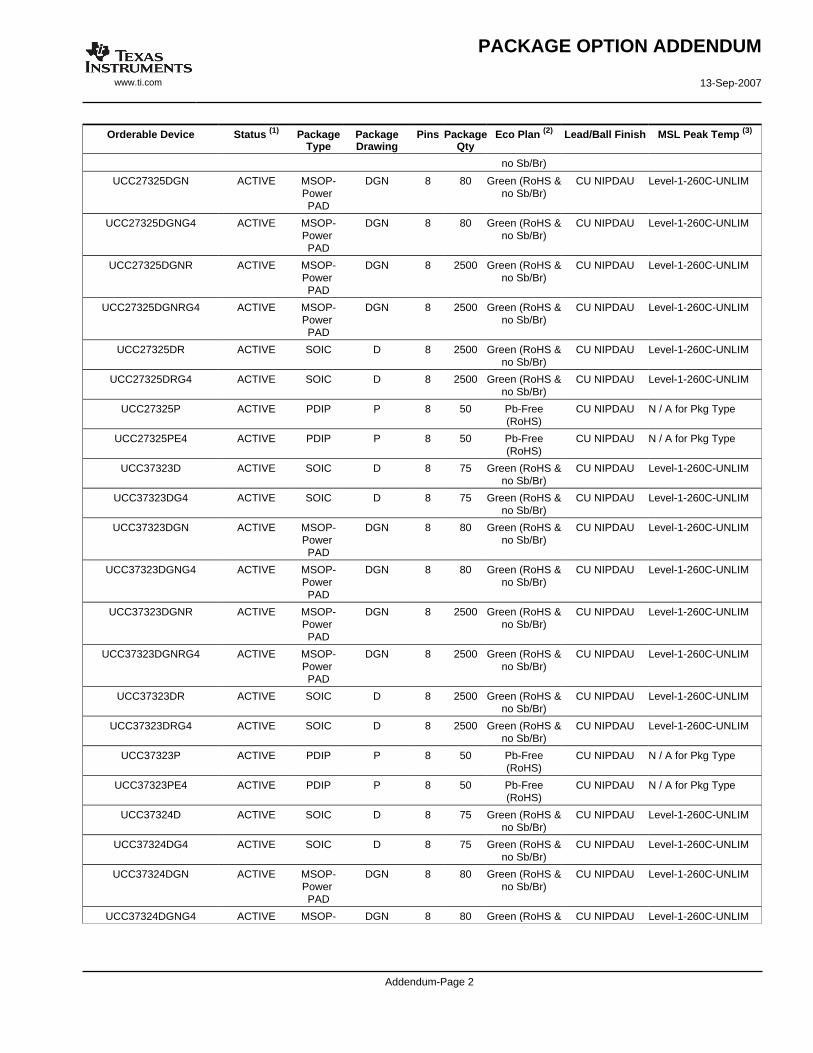
Orderable Device Status (1) PackageType
PackageDrawing
Pins PackageQty
Eco Plan (2) Lead/Ball Finish MSL Peak Temp (3)
no Sb/Br)
UCC27325DGN ACTIVE MSOP-Power PAD
DGN 8 80 Green (RoHS &no Sb/Br)
CU NIPDAU Level-1-260C-UNLIM
UCC27325DGNG4 ACTIVE MSOP-Power PAD
DGN 8 80 Green (RoHS &no Sb/Br)
CU NIPDAU Level-1-260C-UNLIM
UCC27325DGNR ACTIVE MSOP-Power PAD
DGN 8 2500 Green (RoHS &no Sb/Br)
CU NIPDAU Level-1-260C-UNLIM
UCC27325DGNRG4 ACTIVE MSOP-Power PAD
DGN 8 2500 Green (RoHS &no Sb/Br)
CU NIPDAU Level-1-260C-UNLIM
UCC27325DR ACTIVE SOIC D 8 2500 Green (RoHS &no Sb/Br)
CU NIPDAU Level-1-260C-UNLIM
UCC27325DRG4 ACTIVE SOIC D 8 2500 Green (RoHS &no Sb/Br)
CU NIPDAU Level-1-260C-UNLIM
UCC27325P ACTIVE PDIP P 8 50 Pb-Free(RoHS)
CU NIPDAU N / A for Pkg Type
UCC27325PE4 ACTIVE PDIP P 8 50 Pb-Free(RoHS)
CU NIPDAU N / A for Pkg Type
UCC37323D ACTIVE SOIC D 8 75 Green (RoHS &no Sb/Br)
CU NIPDAU Level-1-260C-UNLIM
UCC37323DG4 ACTIVE SOIC D 8 75 Green (RoHS &no Sb/Br)
CU NIPDAU Level-1-260C-UNLIM
UCC37323DGN ACTIVE MSOP-Power PAD
DGN 8 80 Green (RoHS &no Sb/Br)
CU NIPDAU Level-1-260C-UNLIM
UCC37323DGNG4 ACTIVE MSOP-Power PAD
DGN 8 80 Green (RoHS &no Sb/Br)
CU NIPDAU Level-1-260C-UNLIM
UCC37323DGNR ACTIVE MSOP-Power PAD
DGN 8 2500 Green (RoHS &no Sb/Br)
CU NIPDAU Level-1-260C-UNLIM
UCC37323DGNRG4 ACTIVE MSOP-Power PAD
DGN 8 2500 Green (RoHS &no Sb/Br)
CU NIPDAU Level-1-260C-UNLIM
UCC37323DR ACTIVE SOIC D 8 2500 Green (RoHS &no Sb/Br)
CU NIPDAU Level-1-260C-UNLIM
UCC37323DRG4 ACTIVE SOIC D 8 2500 Green (RoHS &no Sb/Br)
CU NIPDAU Level-1-260C-UNLIM
UCC37323P ACTIVE PDIP P 8 50 Pb-Free(RoHS)
CU NIPDAU N / A for Pkg Type
UCC37323PE4 ACTIVE PDIP P 8 50 Pb-Free(RoHS)
CU NIPDAU N / A for Pkg Type
UCC37324D ACTIVE SOIC D 8 75 Green (RoHS &no Sb/Br)
CU NIPDAU Level-1-260C-UNLIM
UCC37324DG4 ACTIVE SOIC D 8 75 Green (RoHS &no Sb/Br)
CU NIPDAU Level-1-260C-UNLIM
UCC37324DGN ACTIVE MSOP-Power PAD
DGN 8 80 Green (RoHS &no Sb/Br)
CU NIPDAU Level-1-260C-UNLIM
UCC37324DGNG4 ACTIVE MSOP- DGN 8 80 Green (RoHS & CU NIPDAU Level-1-260C-UNLIM
PACKAGE OPTION ADDENDUM
www.ti.com 13-Sep-2007
Addendum-Page 2
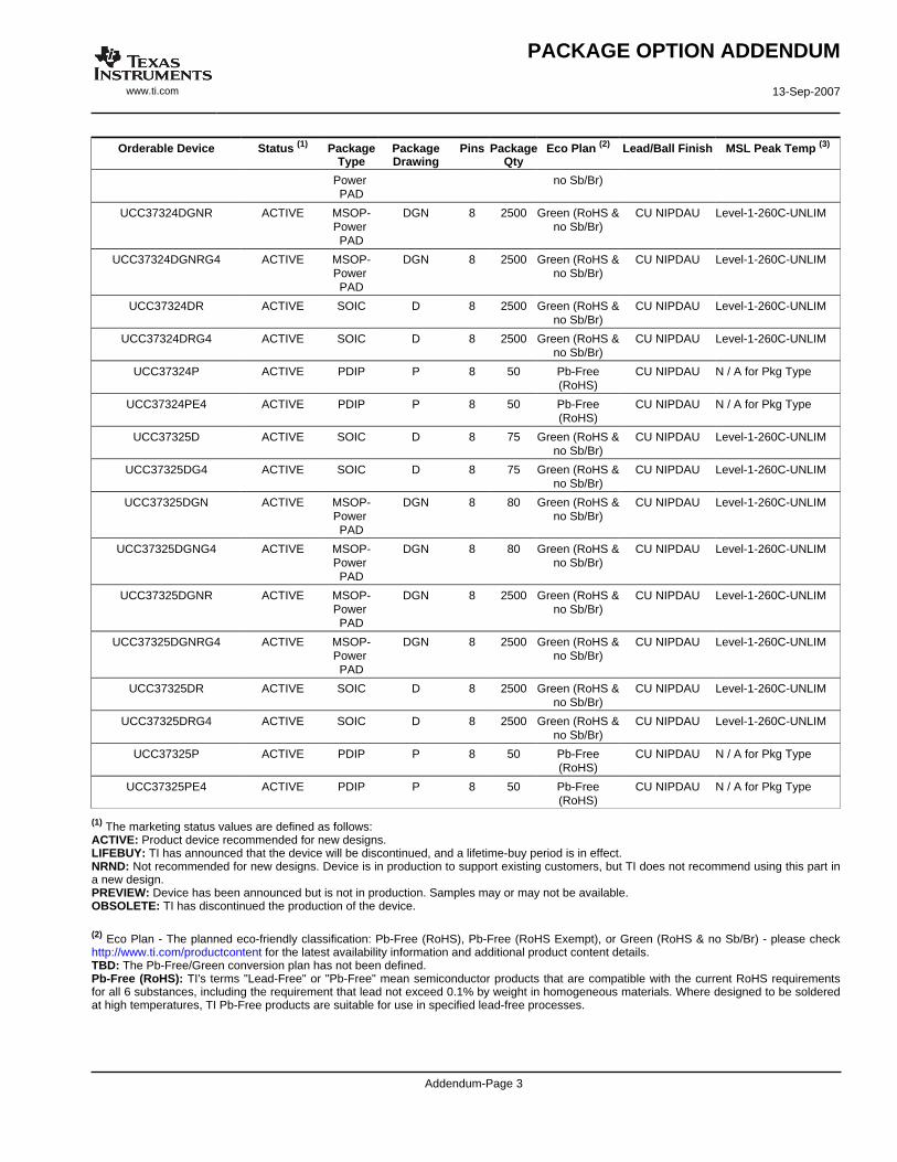
Orderable Device Status (1) PackageType
PackageDrawing
Pins PackageQty
Eco Plan (2) Lead/Ball Finish MSL Peak Temp (3)
Power PAD
no Sb/Br)
UCC37324DGNR ACTIVE MSOP-Power PAD
DGN 8 2500 Green (RoHS &no Sb/Br)
CU NIPDAU Level-1-260C-UNLIM
UCC37324DGNRG4 ACTIVE MSOP-Power PAD
DGN 8 2500 Green (RoHS &no Sb/Br)
CU NIPDAU Level-1-260C-UNLIM
UCC37324DR ACTIVE SOIC D 8 2500 Green (RoHS &no Sb/Br)
CU NIPDAU Level-1-260C-UNLIM
UCC37324DRG4 ACTIVE SOIC D 8 2500 Green (RoHS &no Sb/Br)
CU NIPDAU Level-1-260C-UNLIM
UCC37324P ACTIVE PDIP P 8 50 Pb-Free(RoHS)
CU NIPDAU N / A for Pkg Type
UCC37324PE4 ACTIVE PDIP P 8 50 Pb-Free(RoHS)
CU NIPDAU N / A for Pkg Type
UCC37325D ACTIVE SOIC D 8 75 Green (RoHS &no Sb/Br)
CU NIPDAU Level-1-260C-UNLIM
UCC37325DG4 ACTIVE SOIC D 8 75 Green (RoHS &no Sb/Br)
CU NIPDAU Level-1-260C-UNLIM
UCC37325DGN ACTIVE MSOP-Power PAD
DGN 8 80 Green (RoHS &no Sb/Br)
CU NIPDAU Level-1-260C-UNLIM
UCC37325DGNG4 ACTIVE MSOP-Power PAD
DGN 8 80 Green (RoHS &no Sb/Br)
CU NIPDAU Level-1-260C-UNLIM
UCC37325DGNR ACTIVE MSOP-Power PAD
DGN 8 2500 Green (RoHS &no Sb/Br)
CU NIPDAU Level-1-260C-UNLIM
UCC37325DGNRG4 ACTIVE MSOP-Power PAD
DGN 8 2500 Green (RoHS &no Sb/Br)
CU NIPDAU Level-1-260C-UNLIM
UCC37325DR ACTIVE SOIC D 8 2500 Green (RoHS &no Sb/Br)
CU NIPDAU Level-1-260C-UNLIM
UCC37325DRG4 ACTIVE SOIC D 8 2500 Green (RoHS &no Sb/Br)
CU NIPDAU Level-1-260C-UNLIM
UCC37325P ACTIVE PDIP P 8 50 Pb-Free(RoHS)
CU NIPDAU N / A for Pkg Type
UCC37325PE4 ACTIVE PDIP P 8 50 Pb-Free(RoHS)
CU NIPDAU N / A for Pkg Type
(1) The marketing status values are defined as follows:ACTIVE: Product device recommended for new designs.LIFEBUY: TI has announced that the device will be discontinued, and a lifetime-buy period is in effect.NRND: Not recommended for new designs. Device is in production to support existing customers, but TI does not recommend using this part ina new design.PREVIEW: Device has been announced but is not in production. Samples may or may not be available.OBSOLETE: TI has discontinued the production of the device.
(2) Eco Plan - The planned eco-friendly classification: Pb-Free (RoHS), Pb-Free (RoHS Exempt), or Green (RoHS & no Sb/Br) - please checkhttp://www.ti.com/productcontent for the latest availability information and additional product content details.TBD: The Pb-Free/Green conversion plan has not been defined.Pb-Free (RoHS): TI's terms "Lead-Free" or "Pb-Free" mean semiconductor products that are compatible with the current RoHS requirementsfor all 6 substances, including the requirement that lead not exceed 0.1% by weight in homogeneous materials. Where designed to be solderedat high temperatures, TI Pb-Free products are suitable for use in specified lead-free processes.
PACKAGE OPTION ADDENDUM
www.ti.com 13-Sep-2007
Addendum-Page 3
Pb-Free (RoHS Exempt): This component has a RoHS exemption for either 1) lead-based flip-chip solder bumps used between the die andpackage, or 2) lead-based die adhesive used between the die and leadframe. The component is otherwise considered Pb-Free (RoHScompatible) as defined above.Green (RoHS & no Sb/Br): TI defines "Green" to mean Pb-Free (RoHS compatible), and free of Bromine (Br) and Antimony (Sb) based flameretardants (Br or Sb do not exceed 0.1% by weight in homogeneous material)
(3) MSL, Peak Temp. -- The Moisture Sensitivity Level rating according to the JEDEC industry standard classifications, and peak soldertemperature.
Important Information and Disclaimer:The information provided on this page represents TI's knowledge and belief as of the date that it isprovided. TI bases its knowledge and belief on information provided by third parties, and makes no representation or warranty as to theaccuracy of such information. Efforts are underway to better integrate information from third parties. TI has taken and continues to takereasonable steps to provide representative and accurate information but may not have conducted destructive testing or chemical analysis onincoming materials and chemicals. TI and TI suppliers consider certain information to be proprietary, and thus CAS numbers and other limitedinformation may not be available for release.
In no event shall TI's liability arising out of such information exceed the total purchase price of the TI part(s) at issue in this document sold by TIto Customer on an annual basis.
PACKAGE OPTION ADDENDUM
www.ti.com 13-Sep-2007
Addendum-Page 4
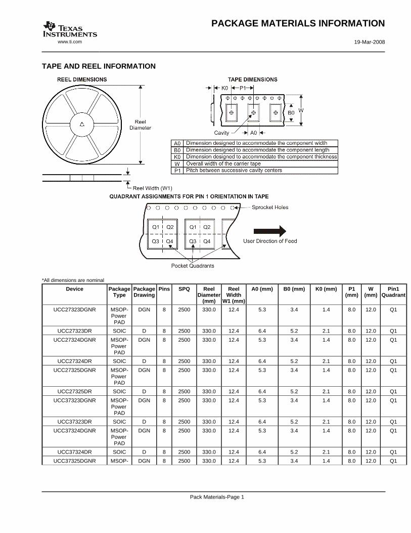
TAPE AND REEL INFORMATION
*All dimensions are nominal
Device PackageType
PackageDrawing
Pins SPQ ReelDiameter
(mm)
ReelWidth
W1 (mm)
A0 (mm) B0 (mm) K0 (mm) P1(mm)
W(mm)
Pin1Quadrant
UCC27323DGNR MSOP-Power PAD
DGN 8 2500 330.0 12.4 5.3 3.4 1.4 8.0 12.0 Q1
UCC27323DR SOIC D 8 2500 330.0 12.4 6.4 5.2 2.1 8.0 12.0 Q1
UCC27324DGNR MSOP-Power PAD
DGN 8 2500 330.0 12.4 5.3 3.4 1.4 8.0 12.0 Q1
UCC27324DR SOIC D 8 2500 330.0 12.4 6.4 5.2 2.1 8.0 12.0 Q1
UCC27325DGNR MSOP-Power PAD
DGN 8 2500 330.0 12.4 5.3 3.4 1.4 8.0 12.0 Q1
UCC27325DR SOIC D 8 2500 330.0 12.4 6.4 5.2 2.1 8.0 12.0 Q1
UCC37323DGNR MSOP-Power PAD
DGN 8 2500 330.0 12.4 5.3 3.4 1.4 8.0 12.0 Q1
UCC37323DR SOIC D 8 2500 330.0 12.4 6.4 5.2 2.1 8.0 12.0 Q1
UCC37324DGNR MSOP-Power PAD
DGN 8 2500 330.0 12.4 5.3 3.4 1.4 8.0 12.0 Q1
UCC37324DR SOIC D 8 2500 330.0 12.4 6.4 5.2 2.1 8.0 12.0 Q1
UCC37325DGNR MSOP- DGN 8 2500 330.0 12.4 5.3 3.4 1.4 8.0 12.0 Q1
PACKAGE MATERIALS INFORMATION
www.ti.com 19-Mar-2008
Pack Materials-Page 1
Device PackageType
PackageDrawing
Pins SPQ ReelDiameter
(mm)
ReelWidth
W1 (mm)
A0 (mm) B0 (mm) K0 (mm) P1(mm)
W(mm)
Pin1Quadrant
Power PAD
UCC37325DR SOIC D 8 2500 330.0 12.4 6.4 5.2 2.1 8.0 12.0 Q1
*All dimensions are nominal
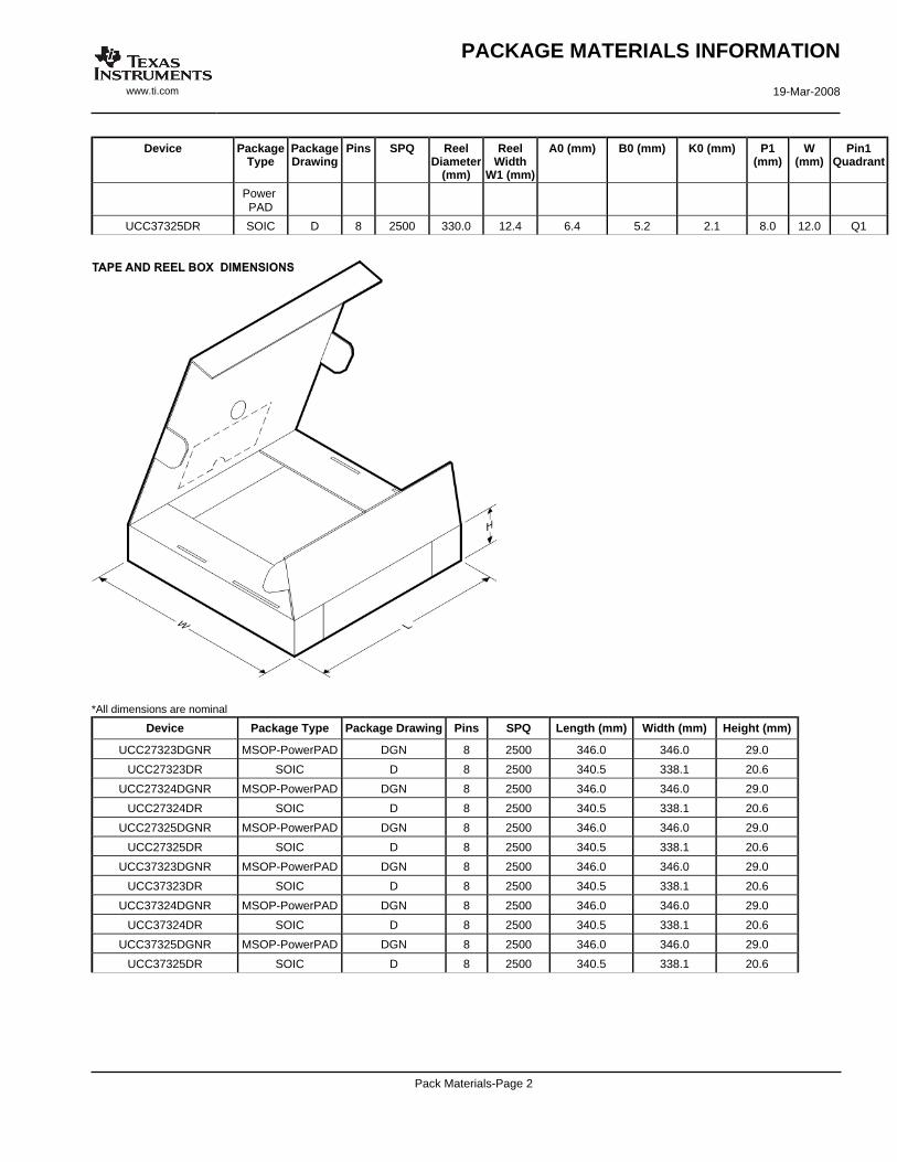
Device Package Type Package Drawing Pins SPQ Length (mm) Width (mm) Height (mm)
UCC27323DGNR MSOP-PowerPAD DGN 8 2500 346.0 346.0 29.0
UCC27323DR SOIC D 8 2500 340.5 338.1 20.6
UCC27324DGNR MSOP-PowerPAD DGN 8 2500 346.0 346.0 29.0
UCC27324DR SOIC D 8 2500 340.5 338.1 20.6
UCC27325DGNR MSOP-PowerPAD DGN 8 2500 346.0 346.0 29.0
UCC27325DR SOIC D 8 2500 340.5 338.1 20.6
UCC37323DGNR MSOP-PowerPAD DGN 8 2500 346.0 346.0 29.0
UCC37323DR SOIC D 8 2500 340.5 338.1 20.6
UCC37324DGNR MSOP-PowerPAD DGN 8 2500 346.0 346.0 29.0
UCC37324DR SOIC D 8 2500 340.5 338.1 20.6
UCC37325DGNR MSOP-PowerPAD DGN 8 2500 346.0 346.0 29.0
UCC37325DR SOIC D 8 2500 340.5 338.1 20.6
PACKAGE MATERIALS INFORMATION
www.ti.com 19-Mar-2008
Pack Materials-Page 2
MECHANICAL DATA
MPDI001A – JANUARY 1995 – REVISED JUNE 1999
POST OFFICE BOX 655303 • DALLAS, TEXAS 75265
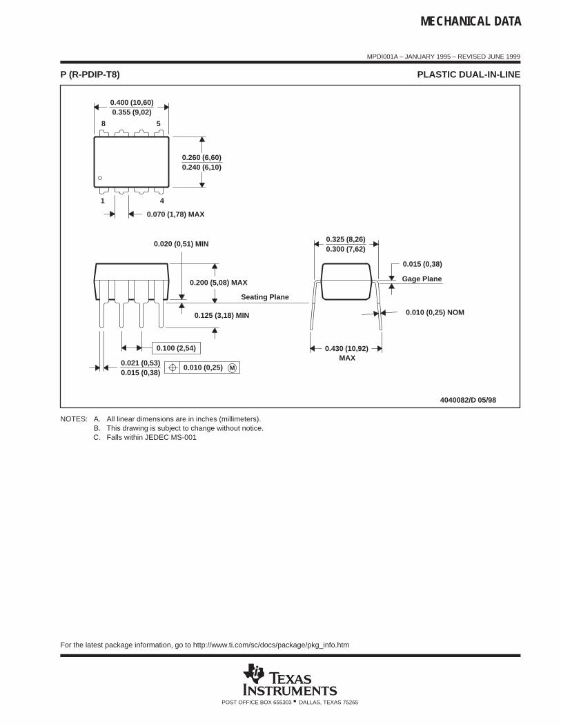
P (R-PDIP-T8) PLASTIC DUAL-IN-LINE
8
4
0.015 (0,38)
Gage Plane
0.325 (8,26)0.300 (7,62)
0.010 (0,25) NOM
MAX0.430 (10,92)
4040082/D 05/98
0.200 (5,08) MAX
0.125 (3,18) MIN
5
0.355 (9,02)
0.020 (0,51) MIN
0.070 (1,78) MAX
0.240 (6,10)0.260 (6,60)
0.400 (10,60)
1
0.015 (0,38)0.021 (0,53)
Seating Plane
M0.010 (0,25)
0.100 (2,54)
NOTES: A. All linear dimensions are in inches (millimeters).B. This drawing is subject to change without notice.C. Falls within JEDEC MS-001
For the latest package information, go to http://www.ti.com/sc/docs/package/pkg_info.htm
IMPORTANT NOTICETexas Instruments Incorporated and its subsidiaries (TI) reserve the right to make corrections, modifications, enhancements, improvements,and other changes to its products and services at any time and to discontinue any product or service without notice. Customers shouldobtain the latest relevant information before placing orders and should verify that such information is current and complete. All products aresold subject to TI’s terms and conditions of sale supplied at the time of order acknowledgment.TI warrants performance of its hardware products to the specifications applicable at the time of sale in accordance with TI’s standardwarranty. Testing and other quality control techniques are used to the extent TI deems necessary to support this warranty. Except wheremandated by government requirements, testing of all parameters of each product is not necessarily performed.TI assumes no liability for applications assistance or customer product design. Customers are responsible for their products andapplications using TI components. To minimize the risks associated with customer products and applications, customers should provideadequate design and operating safeguards.TI does not warrant or represent that any license, either express or implied, is granted under any TI patent right, copyright, mask work right,or other TI intellectual property right relating to any combination, machine, or process in which TI products or services are used. Informationpublished by TI regarding third-party products or services does not constitute a license from TI to use such products or services or awarranty or endorsement thereof. Use of such information may require a license from a third party under the patents or other intellectualproperty of the third party, or a license from TI under the patents or other intellectual property of TI.Reproduction of TI information in TI data books or data sheets is permissible only if reproduction is without alteration and is accompaniedby all associated warranties, conditions, limitations, and notices. Reproduction of this information with alteration is an unfair and deceptivebusiness practice. TI is not responsible or liable for such altered documentation. Information of third parties may be subject to additionalrestrictions.Resale of TI products or services with statements different from or beyond the parameters stated by TI for that product or service voids allexpress and any implied warranties for the associated TI product or service and is an unfair and deceptive business practice. TI is notresponsible or liable for any such statements.TI products are not authorized for use in safety-critical applications (such as life support) where a failure of the TI product would reasonablybe expected to cause severe personal injury or death, unless officers of the parties have executed an agreement specifically governingsuch use. Buyers represent that they have all necessary expertise in the safety and regulatory ramifications of their applications, andacknowledge and agree that they are solely responsible for all legal, regulatory and safety-related requirements concerning their productsand any use of TI products in such safety-critical applications, notwithstanding any applications-related information or support that may beprovided by TI. Further, Buyers must fully indemnify TI and its representatives against any damages arising out of the use of TI products insuch safety-critical applications.TI products are neither designed nor intended for use in military/aerospace applications or environments unless the TI products arespecifically designated by TI as military-grade or "enhanced plastic." Only products designated by TI as military-grade meet militaryspecifications. Buyers acknowledge and agree that any such use of TI products which TI has not designated as military-grade is solely atthe Buyer's risk, and that they are solely responsible for compliance with all legal and regulatory requirements in connection with such use.TI products are neither designed nor intended for use in automotive applications or environments unless the specific TI products aredesignated by TI as compliant with ISO/TS 16949 requirements. Buyers acknowledge and agree that, if they use any non-designatedproducts in automotive applications, TI will not be responsible for any failure to meet such requirements.Following are URLs where you can obtain information on other Texas Instruments products and application solutions:Products ApplicationsAmplifiers amplifier.ti.com Audio www.ti.com/audioData Converters dataconverter.ti.com Automotive www.ti.com/automotiveDSP dsp.ti.com Broadband www.ti.com/broadbandClocks and Timers www.ti.com/clocks Digital Control www.ti.com/digitalcontrolInterface interface.ti.com Medical www.ti.com/medicalLogic logic.ti.com Military www.ti.com/militaryPower Mgmt power.ti.com Optical Networking www.ti.com/opticalnetworkMicrocontrollers microcontroller.ti.com Security www.ti.com/securityRFID www.ti-rfid.com Telephony www.ti.com/telephonyRF/IF and ZigBee® Solutions www.ti.com/lprf Video & Imaging www.ti.com/video
Wireless www.ti.com/wireless
Mailing Address: Texas Instruments, Post Office Box 655303, Dallas, Texas 75265Copyright © 2008, Texas Instruments Incorporated


![AtletIQ.com — тренируйся с умом! [версия для печати]€¦ · 3 Bent-Arm Dumbbell Pullover 4 10-15 60-90 sec 4 Wide-Grip Pulldown Behind The Neck 4](https://img.pdfslide.tips/doc/110x75/5f0b0dee7e708231d42e9fe9/a-f-f-3-bent-arm.jpg)


![AtletIQ.com — тренируйся с умом! [версия для печати] · Wide-Grip Lat Pulldown Powe r ati ls Dumbbell Flyes Weighted Bench Dip L egExt nsio Barbell](https://img.pdfslide.tips/doc/110x75/5f9ae69f5a010e7af47401df/a-f-f-wide-grip.jpg)