Embed Size (px)
Citation preview
1
Chapter 9 Counter/Timer Programming in the
8051
2
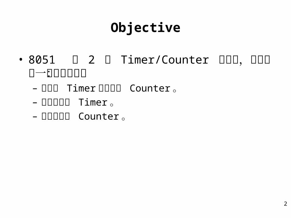
Objective
• 8051 有 2 個 Timer/Counter 的機制,我們在這一章裡要瞭解:– 什麼是 Timer ,什麼是 Counter 。– 如何來使用 Timer 。– 如何來使用 Counter 。
3
Sections
9.1 Programming 8051 Timers
9.2 Counter Programming
4
Section 9.1Programming 8051 Timers
5
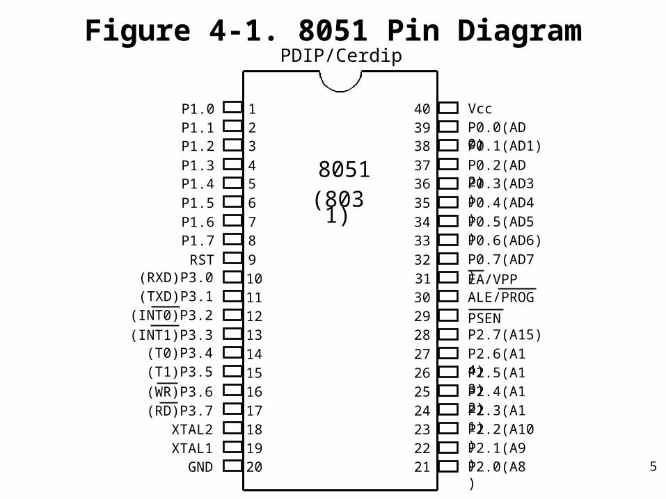
Figure 4-1. 8051 Pin DiagramPDIP/Cerdip
123
4567891011121314151617181920
403938
3736353433323130292827262524232221
P1.0P1.1P1.2
P1.3P1.4P1.5P1.6P1.7RST
(RXD)P3.0(TXD)P3.1
(T0)P3.4(T1)P3.5
XTAL2XTAL1
GND
(INT0)P3.2
(INT1)P3.3
(RD)P3.7(WR)P3.6
VccP0.0(AD0)P0.1(AD1)
P0.2(AD2)P0.3(AD3)P0.4(AD4)P0.5(AD5)P0.6(AD6)P0.7(AD7)
EA/VPPALE/PROG
PSENP2.7(A15)P2.6(A14)P2.5(A13)P2.4(A12)P2.3(A11)P2.2(A10)P2.1(A9)P2.0(A8)
8051(8031)
6
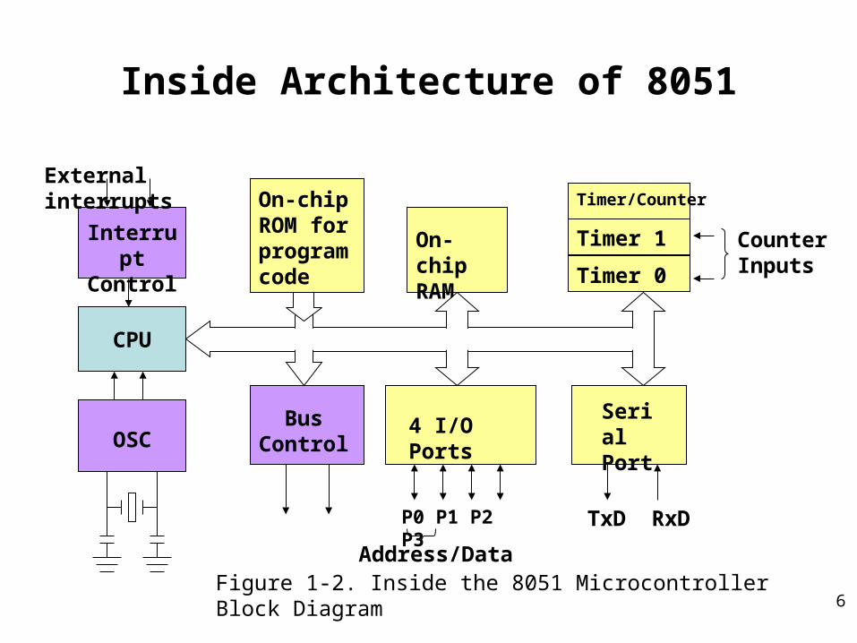
Inside Architecture of 8051
CPU
On-chip RAM
On-chip ROM for program code
4 I/O Ports
Timer 0
Serial Port
Figure 1-2. Inside the 8051 Microcontroller Block Diagram
OSC
Interrupt Control
External interrupts
Timer 1
Timer/Counter
Bus Control
TxD RxDP0 P1 P2 P3
Address/Data
Counter Inputs
7
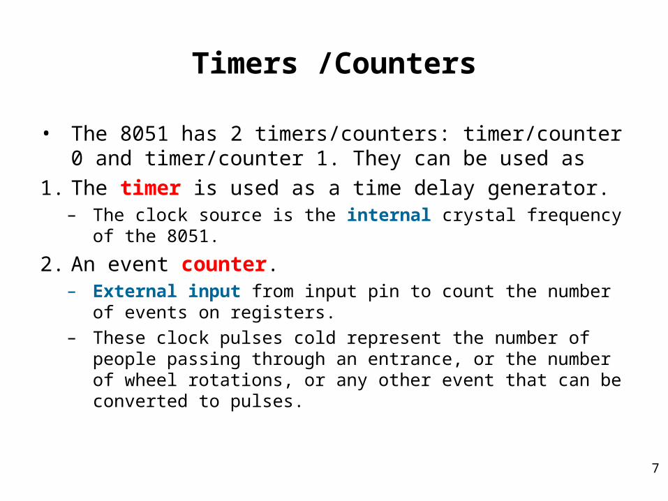
Timers /Counters
• The 8051 has 2 timers/counters: timer/counter 0 and timer/counter 1. They can be used as
1. The timer is used as a time delay generator.– The clock source is the internal crystal frequency of the 8051.
2. An event counter.– External input from input pin to count the number of events
on registers.
– These clock pulses cold represent the number of people passing through an entrance, or the number of wheel rotations, or any other event that can be converted to pulses.
8
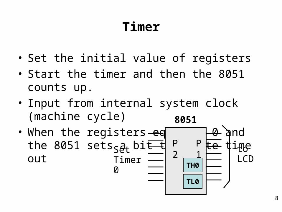
Timer
• Set the initial value of registers• Start the timer and then the 8051 counts up.• Input from internal system clock (machine cycle)• When the registers equal to 0 and the 8051 sets a
bit to denote time out
toLCD
P1
8051
TL0
TH0
P2SetTimer 0
9
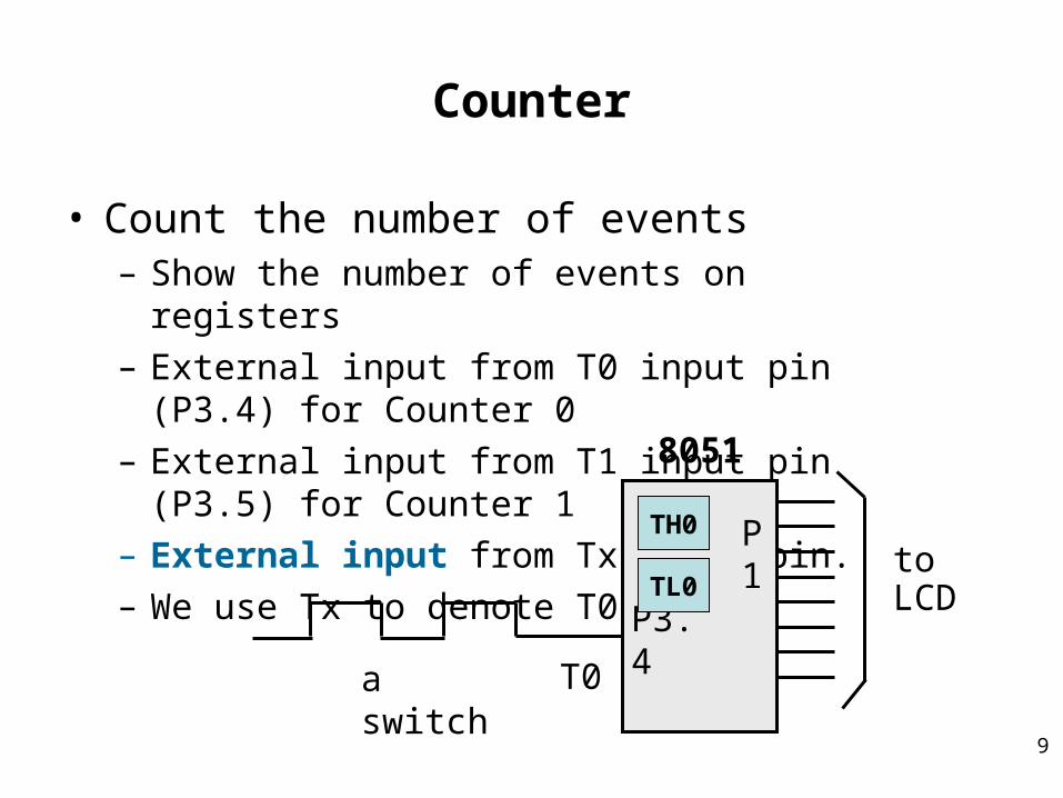
Counter
• Count the number of events– Show the number of events on registers
– External input from T0 input pin (P3.4) for Counter 0
– External input from T1 input pin (P3.5) for Counter 1
– External input from Tx input pin.
– We use Tx to denote T0 or T1.
T0
toLCD
P3.4
P1
8051
a switch
TL0
TH0
10
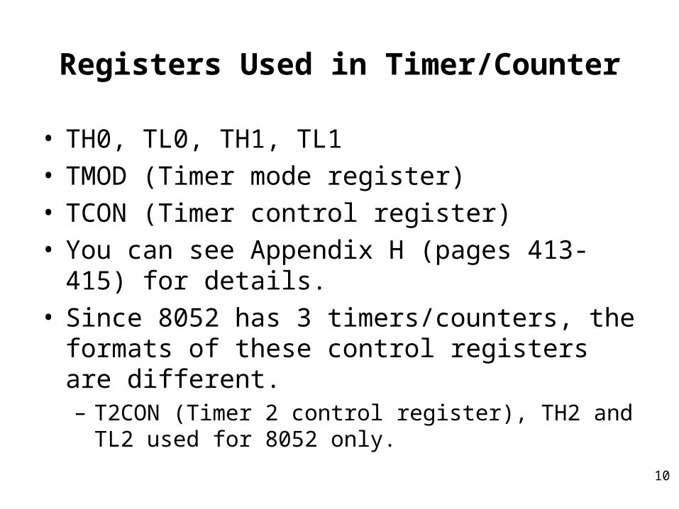
Registers Used in Timer/Counter
• TH0, TL0, TH1, TL1 • TMOD (Timer mode register)• TCON (Timer control register)• You can see Appendix H (pages 413-415) for details.• Since 8052 has 3 timers/counters, the formats of these
control registers are different. – T2CON (Timer 2 control register), TH2 and TL2 used for
8052 only.
11
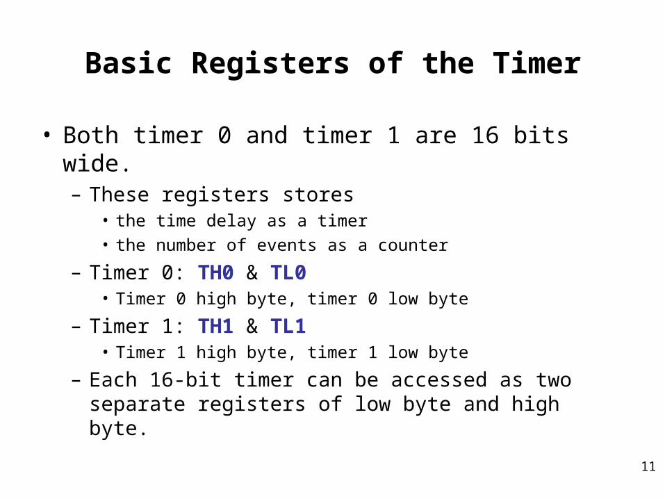
Basic Registers of the Timer
• Both timer 0 and timer 1 are 16 bits wide.– These registers stores
• the time delay as a timer
• the number of events as a counter
– Timer 0: TH0 & TL0• Timer 0 high byte, timer 0 low byte
– Timer 1: TH1 & TL1• Timer 1 high byte, timer 1 low byte
– Each 16-bit timer can be accessed as two separate registers of low byte and high byte.
12
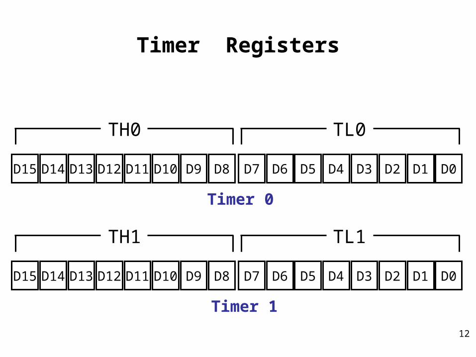
Timer Registers
D15 D8D9D10D11D12D13D14 D7 D0D1D2D3D4D5D6
TH0 TL0
D15 D8D9D10D11D12D13D14 D7 D0D1D2D3D4D5D6
TH1 TL1
Timer 0
Timer 1
13
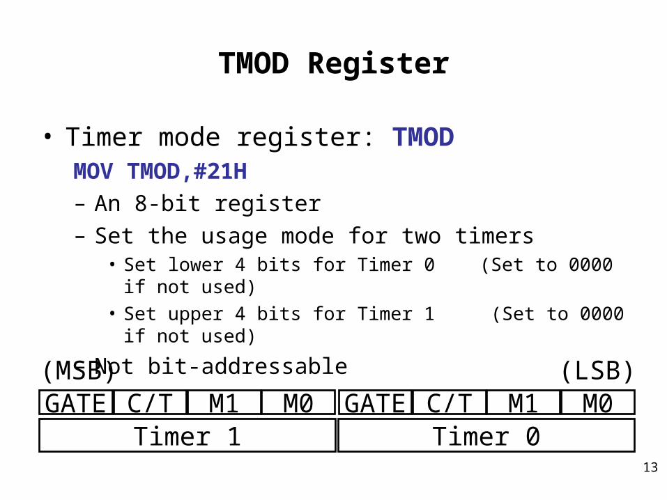
TMOD Register
• Timer mode register: TMODMOV TMOD,#21H– An 8-bit register
– Set the usage mode for two timers • Set lower 4 bits for Timer 0 (Set to 0000 if not used)
• Set upper 4 bits for Timer 1 (Set to 0000 if not used)
– Not bit-addressable
GATE C/T M1 M0 GATE C/T M1 M0Timer 1 Timer 0
(MSB) (LSB)
14
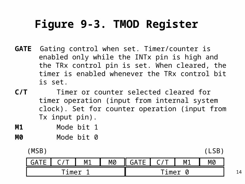
Figure 9-3. TMOD Register
GATE Gating control when set. Timer/counter is enabled only while the INTx pin is high and the TRx control pin is set. When cleared, the timer is enabled whenever the TRx control bit is set.
C/T Timer or counter selected cleared for timer operation (input from internal system clock). Set for counter operation (input from Tx input pin).
M1 Mode bit 1
M0 Mode bit 0
GATE C/T M1 M0 GATE C/T M1 M0
Timer 1 Timer 0
(MSB) (LSB)
15
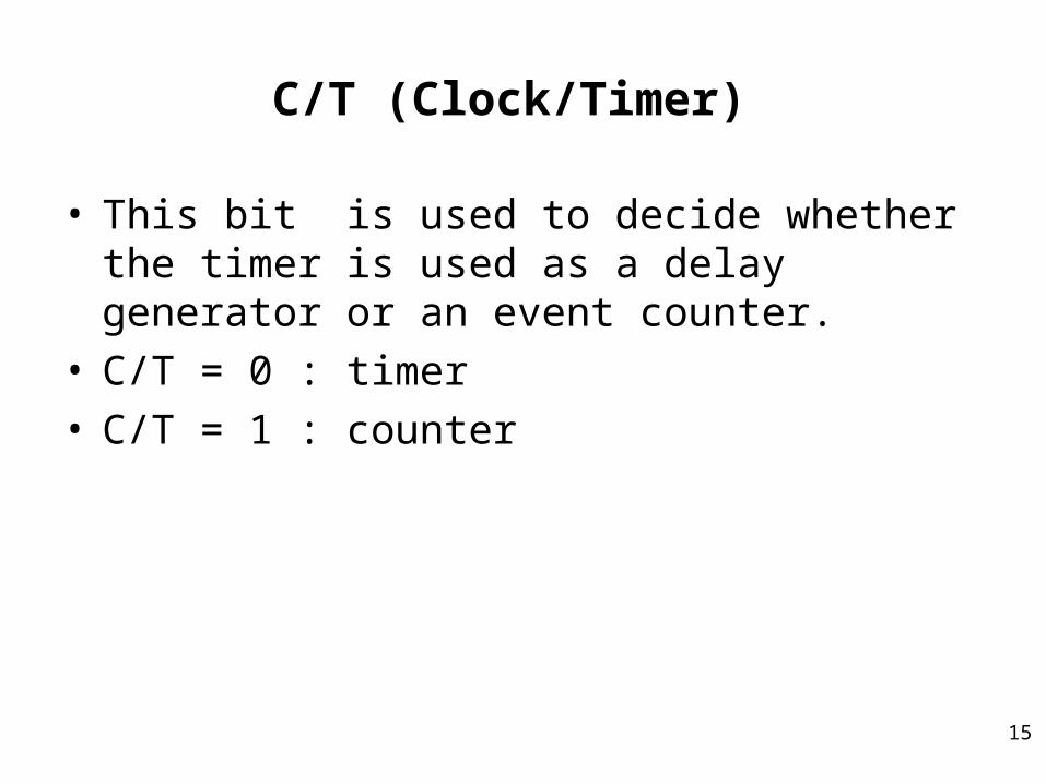
C/T (Clock/Timer)
• This bit is used to decide whether the timer is used as a delay generator or an event counter.
• C/T = 0 : timer• C/T = 1 : counter
16
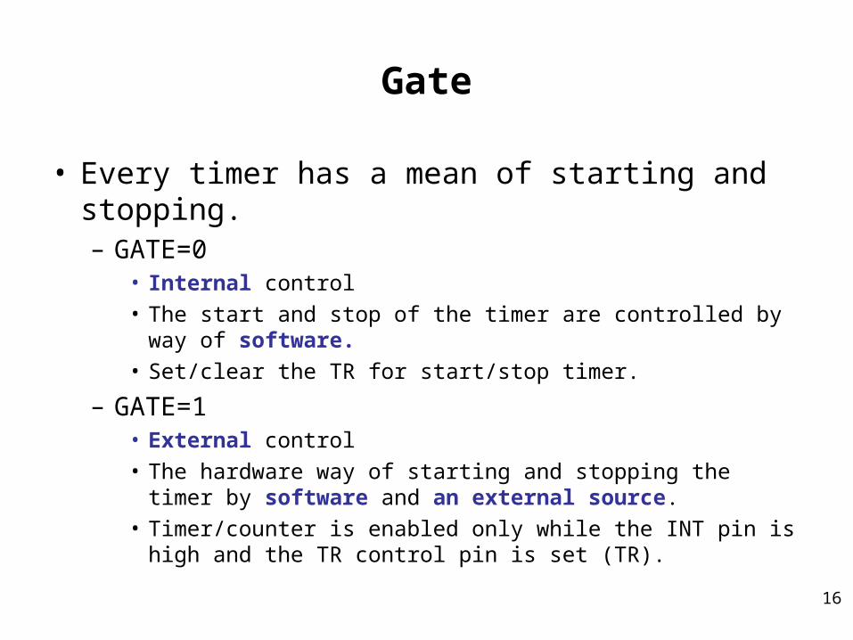
Gate
• Every timer has a mean of starting and stopping.– GATE=0
• Internal control
• The start and stop of the timer are controlled by way of software.
• Set/clear the TR for start/stop timer.
– GATE=1• External control
• The hardware way of starting and stopping the timer by software and an external source.
• Timer/counter is enabled only while the INT pin is high and the TR control pin is set (TR).
17
M1, M0
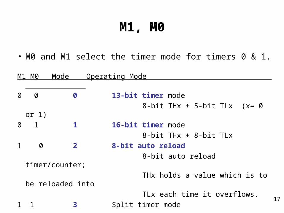
• M0 and M1 select the timer mode for timers 0 & 1.
M1 M0 Mode Operating Mode
0 0 0 13-bit timer mode
8-bit THx + 5-bit TLx (x= 0 or 1)
0 1 1 16-bit timer mode
8-bit THx + 8-bit TLx
1 0 2 8-bit auto reload
8-bit auto reload timer/counter;
THx holds a value which is to be reloaded into
TLx each time it overflows.
1 1 3 Split timer mode
18
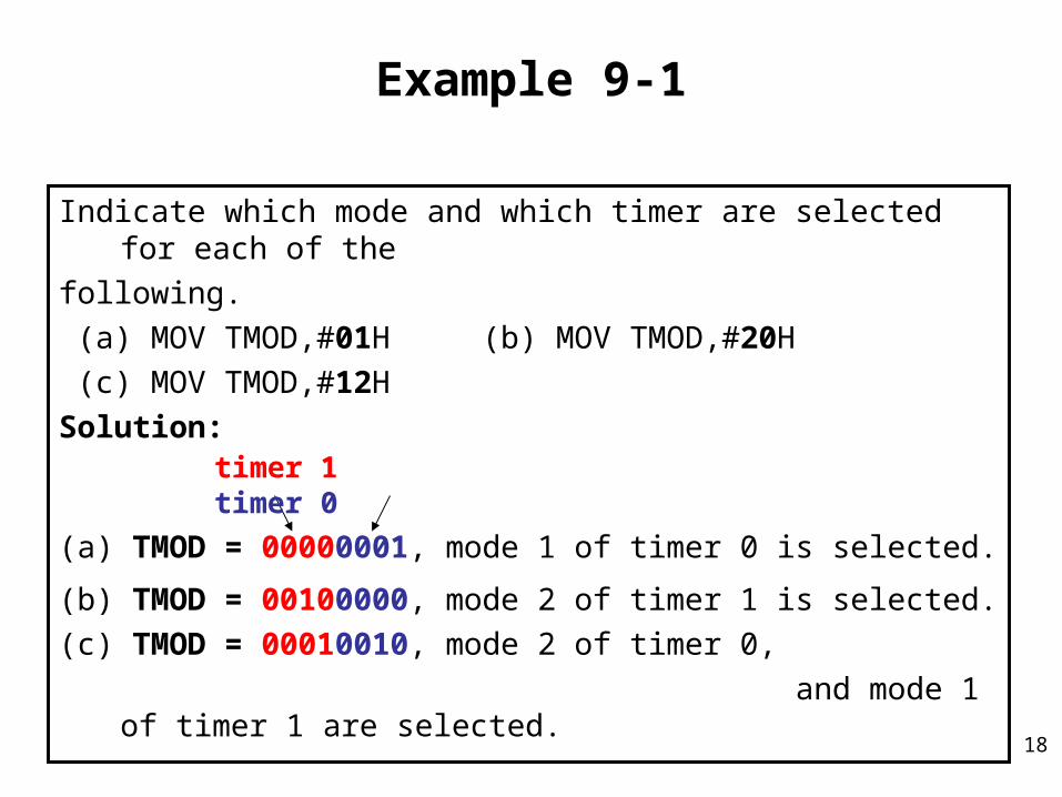
Example 9-1
Indicate which mode and which timer are selected for each of the
following.
(a) MOV TMOD,#01H (b) MOV TMOD,#20H
(c) MOV TMOD,#12H
Solution:
(a) TMOD = 00000001, mode 1 of timer 0 is selected.
(b) TMOD = 00100000, mode 2 of timer 1 is selected.
(c) TMOD = 00010010, mode 2 of timer 0,
and mode 1 of timer 1 are selected.
timer 1 timer 0
19
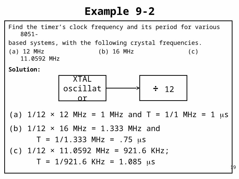
Example 9-2
Find the timer’s clock frequency and its period for various 8051-
based systems, with the following crystal frequencies.
(a) 12 MHz (b) 16 MHz (c) 11.0592 MHz
Solution:
(a) 1/12 × 12 MHz = 1 MHz and T = 1/1 MHz = 1 s
(b) 1/12 × 16 MHz = 1.333 MHz and
T = 1/1.333 MHz = .75 s(c) 1/12 × 11.0592 MHz = 921.6 KHz;
T = 1/921.6 KHz = 1.085 s
XTALoscillator ÷ 12
20
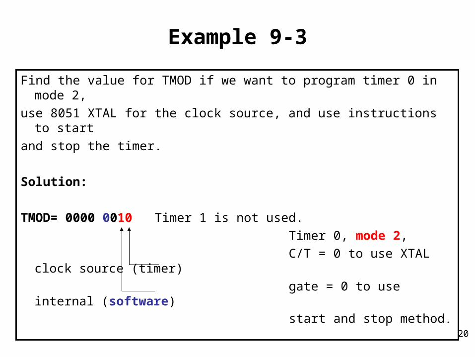
Example 9-3
Find the value for TMOD if we want to program timer 0 in mode 2,
use 8051 XTAL for the clock source, and use instructions to start
and stop the timer.
Solution:
TMOD= 0000 0010 Timer 1 is not used.
Timer 0, mode 2,
C/T = 0 to use XTAL clock source (timer)
gate = 0 to use internal (software)
start and stop method.
21
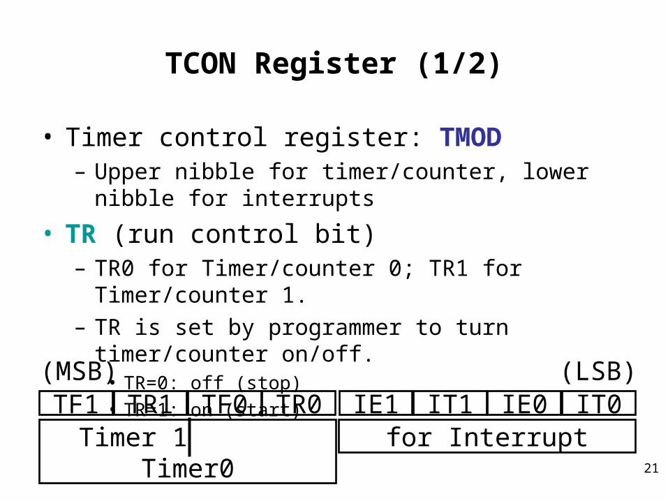
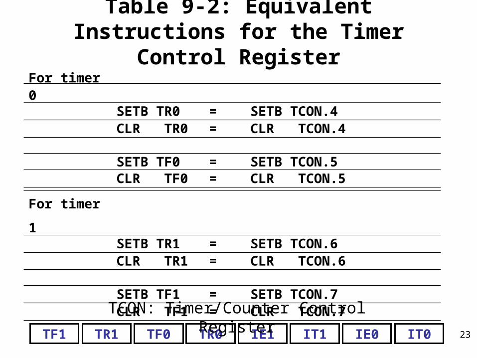
TCON Register (1/2)
• Timer control register: TMOD– Upper nibble for timer/counter, lower nibble for interrupts
• TR (run control bit)– TR0 for Timer/counter 0; TR1 for Timer/counter 1.
– TR is set by programmer to turn timer/counter on/off.• TR=0: off (stop)
• TR=1: on (start)
TF1 TR1 TF0 TR0 IE1 IT1 IE0 IT0Timer 1 Timer0 for Interrupt
(MSB) (LSB)
22
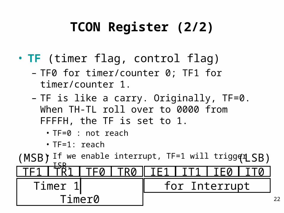
TCON Register (2/2)
• TF (timer flag, control flag) – TF0 for timer/counter 0; TF1 for timer/counter 1.
– TF is like a carry. Originally, TF=0. When TH-TL roll over to 0000 from FFFFH, the TF is set to 1.
• TF=0 : not reach
• TF=1: reach
• If we enable interrupt, TF=1 will trigger ISR.
TF1 TR1 TF0 TR0 IE1 IT1 IE0 IT0Timer 1 Timer0 for Interrupt
(MSB) (LSB)
23
Table 9-2: Equivalent Instructions for the Timer Control Register
For timer 0SETB TR0 = SETB TCON.4CLR TR0 = CLR TCON.4
SETB TF0 = SETB TCON.5CLR TF0 = CLR TCON.5
For timer 1SETB TR1 = SETB TCON.6CLR TR1 = CLR TCON.6
SETB TF1 = SETB TCON.7CLR TF1 = CLR TCON.7
TF1 IT0IE0IT1IE1TR0TF0TR1
TCON: Timer/Counter Control Register
24
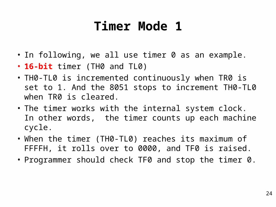
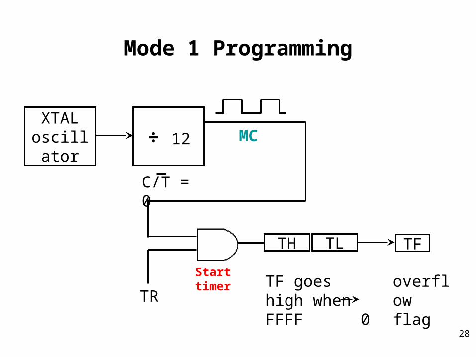
Timer Mode 1
• In following, we all use timer 0 as an example.• 16-bit timer (TH0 and TL0)• TH0-TL0 is incremented continuously when TR0 is set
to 1. And the 8051 stops to increment TH0-TL0 when TR0 is cleared.
• The timer works with the internal system clock. In other words, the timer counts up each machine cycle.
• When the timer (TH0-TL0) reaches its maximum of FFFFH, it rolls over to 0000, and TF0 is raised.
• Programmer should check TF0 and stop the timer 0.
25
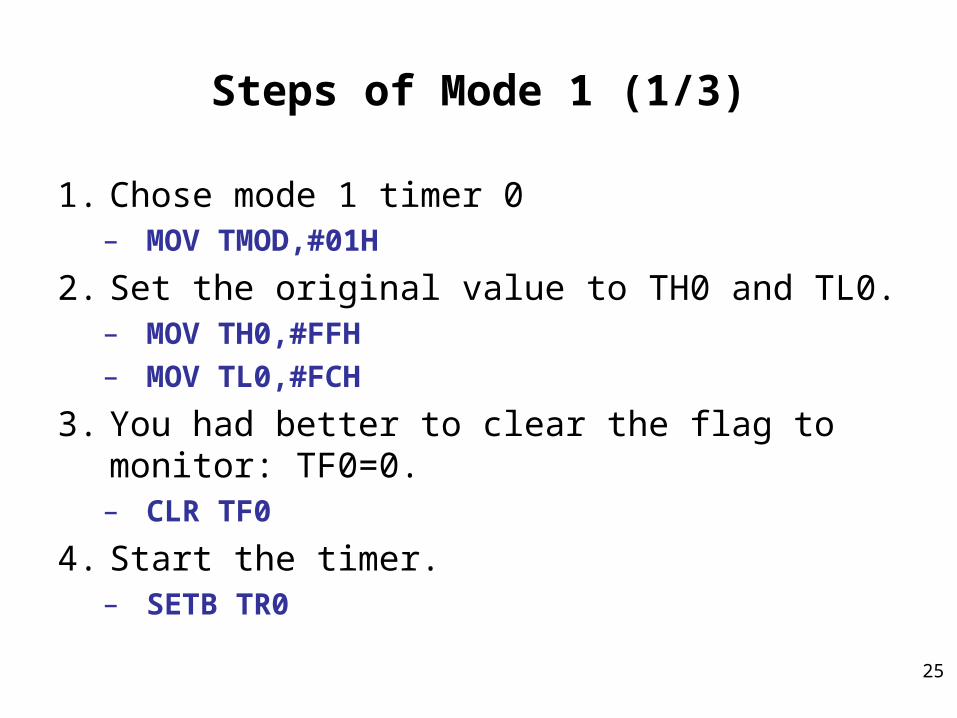
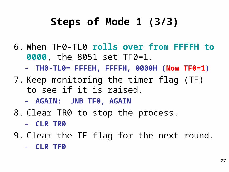
Steps of Mode 1 (1/3)
1. Chose mode 1 timer 0– MOV TMOD,#01H
2. Set the original value to TH0 and TL0.– MOV TH0,#FFH– MOV TL0,#FCH
3. You had better to clear the flag to monitor: TF0=0.– CLR TF0
4. Start the timer.– SETB TR0
26
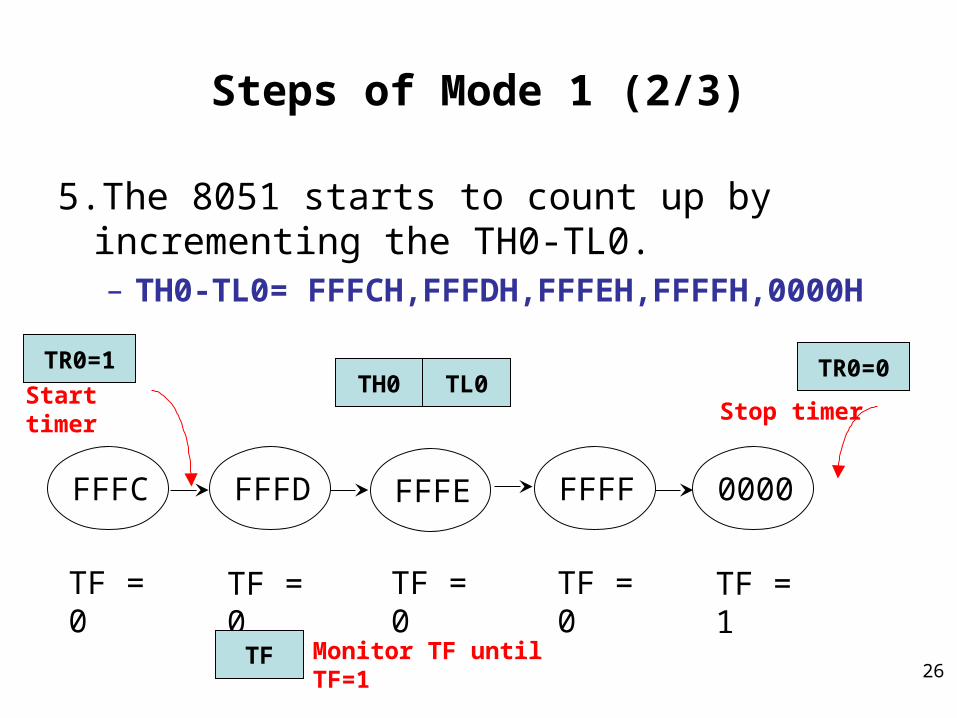
Steps of Mode 1 (2/3)
5. The 8051 starts to count up by incrementing the TH0-TL0.– TH0-TL0= FFFCH,FFFDH,FFFEH,FFFFH,0000H
FFFC FFFD FFFE FFFF 0000
TF = 0 TF = 0 TF = 0 TF = 0 TF = 1
TH0 TL0Start timerStop timer
Monitor TF until TF=1
TR0=1 TR0=0
TF
27
Steps of Mode 1 (3/3)
6. When TH0-TL0 rolls over from FFFFH to 0000, the 8051 set TF0=1. – TH0-TL0= FFFEH, FFFFH, 0000H (Now TF0=1)
7. Keep monitoring the timer flag (TF) to see if it is raised.– AGAIN: JNB TF0, AGAIN
8. Clear TR0 to stop the process.– CLR TR0
9. Clear the TF flag for the next round.– CLR TF0
28
Mode 1 Programming
XTALoscillator ÷ 12
TR
TH TL TF
TF goes high when FFFF 0
overflow flag
C/T = 0
MC
Start timer
29
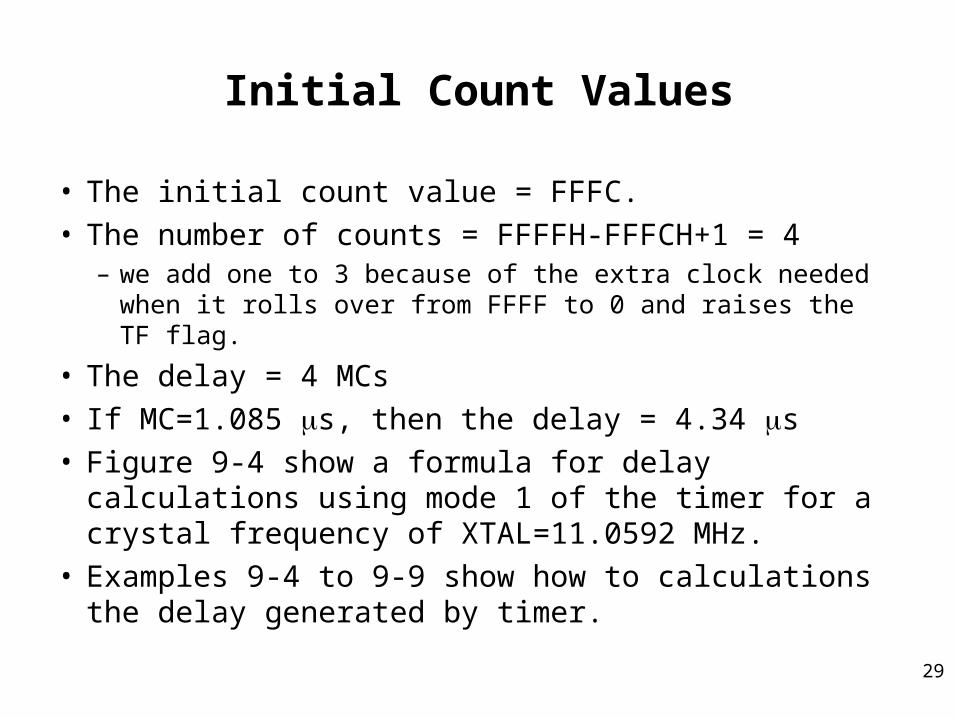
Initial Count Values
• The initial count value = FFFC.• The number of counts = FFFFH-FFFCH+1 = 4
– we add one to 3 because of the extra clock needed when it rolls over from FFFF to 0 and raises the TF flag.
• The delay = 4 MCs• If MC=1.085 s, then the delay = 4.34 s• Figure 9-4 show a formula for delay calculations using
mode 1 of the timer for a crystal frequency of XTAL=11.0592 MHz.
• Examples 9-4 to 9-9 show how to calculations the delay generated by timer.
30
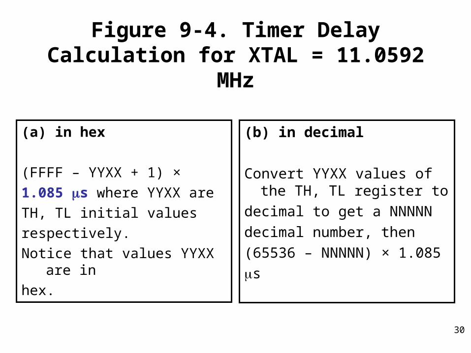
Figure 9-4. Timer Delay Calculation for XTAL = 11.0592 MHz
(a) in hex
(FFFF – YYXX + 1) ×
1.085 s where YYXX are
TH, TL initial values
respectively.
Notice that values YYXX are in
hex.
(b) in decimal
Convert YYXX values of the TH, TL register to
decimal to get a NNNNN
decimal number, then
(65536 – NNNNN) × 1.085
s
31
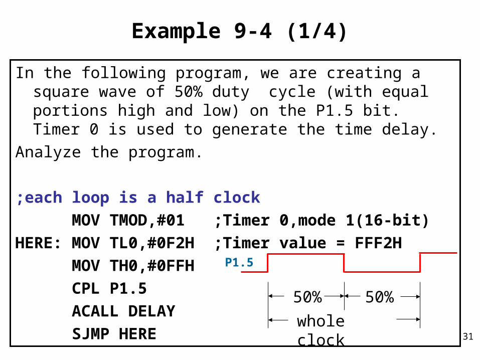
Example 9-4 (1/4)
In the following program, we are creating a square wave of 50% duty cycle (with equal portions high and low) on the P1.5 bit. Timer 0 is used to generate the time delay.
Analyze the program.
;each loop is a half clock
MOV TMOD,#01 ;Timer 0,mode 1(16-bit)
HERE: MOV TL0,#0F2H ;Timer value = FFF2H
MOV TH0,#0FFH
CPL P1.5
ACALL DELAY
SJMP HERE
50% 50%
whole clock
P1.5
32
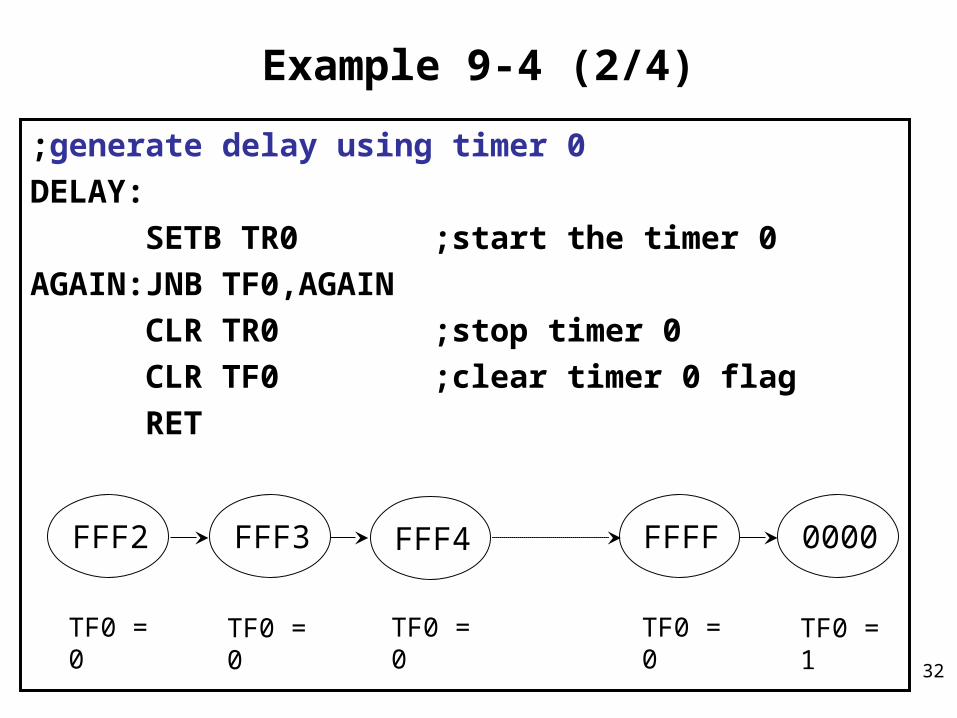
Example 9-4 (2/4)
;generate delay using timer 0
DELAY:
SETB TR0 ;start the timer 0
AGAIN:JNB TF0,AGAIN
CLR TR0 ;stop timer 0
CLR TF0 ;clear timer 0 flag
RET
FFF2 FFF3 FFF4 FFFF 0000
TF0 = 0 TF0 = 0 TF0 = 0 TF0 = 0 TF0 = 1
33
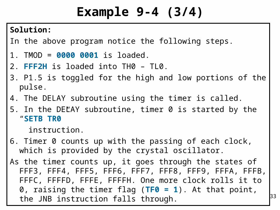
Example 9-4 (3/4)
Solution:
In the above program notice the following steps.
1. TMOD = 0000 0001 is loaded.
2. FFF2H is loaded into TH0 – TL0.
3. P1.5 is toggled for the high and low portions of the pulse.
4. The DELAY subroutine using the timer is called.
5. In the DELAY subroutine, timer 0 is started by the “SETB TR0”
instruction.
6. Timer 0 counts up with the passing of each clock, which is provided by the crystal oscillator.
As the timer counts up, it goes through the states of FFF3, FFF4, FFF5, FFF6, FFF7, FFF8, FFF9, FFFA, FFFB, FFFC, FFFFD, FFFE, FFFFH. One more clock rolls it to 0, raising the timer flag (TF0 = 1). At that point, the JNB instruction falls through.
34
Example 9-4 (4/4)
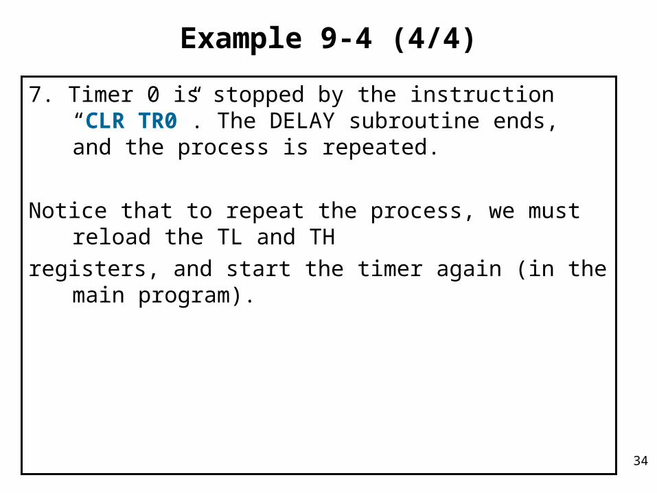
7. Timer 0 is stopped by the instruction “CLR TR0”. The DELAY subroutine ends, and the process is repeated.
Notice that to repeat the process, we must reload the TL and TH
registers, and start the timer again (in the main program).
35
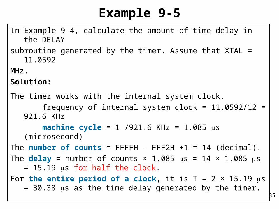
Example 9-5
In Example 9-4, calculate the amount of time delay in the DELAY
subroutine generated by the timer. Assume that XTAL = 11.0592
MHz.
Solution:
The timer works with the internal system clock.
frequency of internal system clock = 11.0592/12 = 921.6 KHz
machine cycle = 1 /921.6 KHz = 1.085 s (microsecond)
The number of counts = FFFFH – FFF2H +1 = 14 (decimal).
The delay = number of counts × 1.085 s = 14 × 1.085 s = 15.19 s for half the clock.
For the entire period of a clock, it is T = 2 × 15.19 s = 30.38 s as the time delay generated by the timer.
36
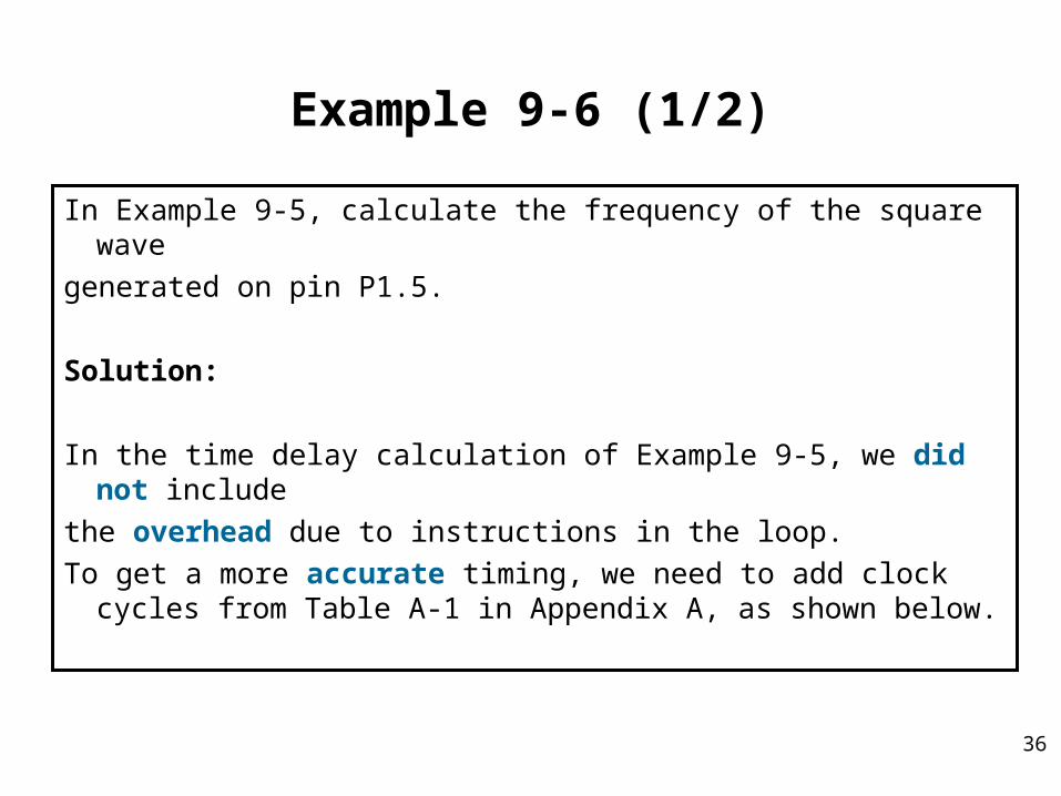
Example 9-6 (1/2)
In Example 9-5, calculate the frequency of the square wave
generated on pin P1.5.
Solution:
In the time delay calculation of Example 9-5, we did not include
the overhead due to instructions in the loop.
To get a more accurate timing, we need to add clock cycles from Table A-1 in Appendix A, as shown below.
37
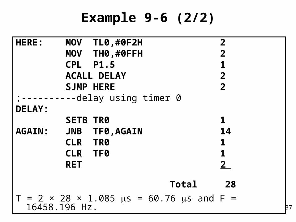
Example 9-6 (2/2)
HERE: MOV TL0,#0F2H 2 MOV TH0,#0FFH 2 CPL P1.5 1 ACALL DELAY 2 SJMP HERE 2;----------delay using timer 0DELAY: SETB TR0 1AGAIN: JNB TF0,AGAIN 14 CLR TR0 1 CLR TF0 1 RET 2 0 Total 28
T = 2 × 28 × 1.085 s = 60.76 s and F = 16458.196 Hz.
38
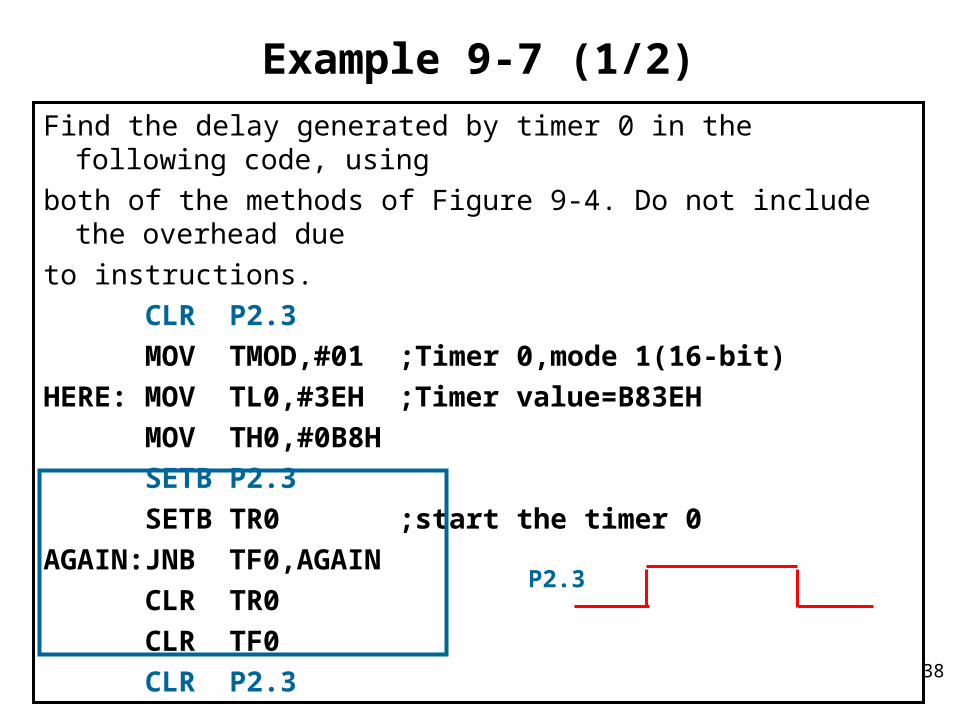
Example 9-7 (1/2)
Find the delay generated by timer 0 in the following code, using
both of the methods of Figure 9-4. Do not include the overhead due
to instructions.
CLR P2.3
MOV TMOD,#01 ;Timer 0,mode 1(16-bit)
HERE: MOV TL0,#3EH ;Timer value=B83EH
MOV TH0,#0B8H
SETB P2.3
SETB TR0 ;start the timer 0
AGAIN:JNB TF0,AGAIN
CLR TR0
CLR TF0
CLR P2.3
P2.3
39
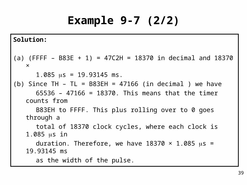
Example 9-7 (2/2)
Solution:
(a) (FFFF – B83E + 1) = 47C2H = 18370 in decimal and 18370 ×
1.085 s = 19.93145 ms.
(b) Since TH – TL = B83EH = 47166 (in decimal ) we have
65536 – 47166 = 18370. This means that the timer counts from
B83EH to FFFF. This plus rolling over to 0 goes through a
total of 18370 clock cycles, where each clock is 1.085 s in
duration. Therefore, we have 18370 × 1.085 s = 19.93145 ms
as the width of the pulse.
40
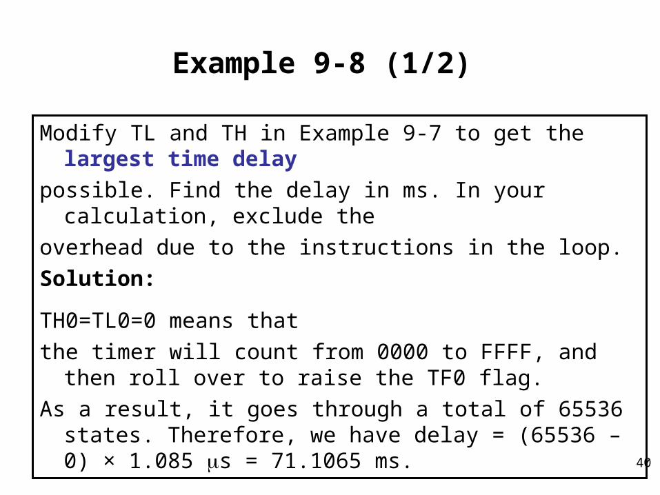
Example 9-8 (1/2)
Modify TL and TH in Example 9-7 to get the largest time delay
possible. Find the delay in ms. In your calculation, exclude the
overhead due to the instructions in the loop.
Solution:
TH0=TL0=0 means that
the timer will count from 0000 to FFFF, and then roll over to raise the TF0 flag.
As a result, it goes through a total of 65536 states. Therefore, we have delay = (65536 – 0) × 1.085 s = 71.1065 ms.
41
Example 9-8 (2/2)
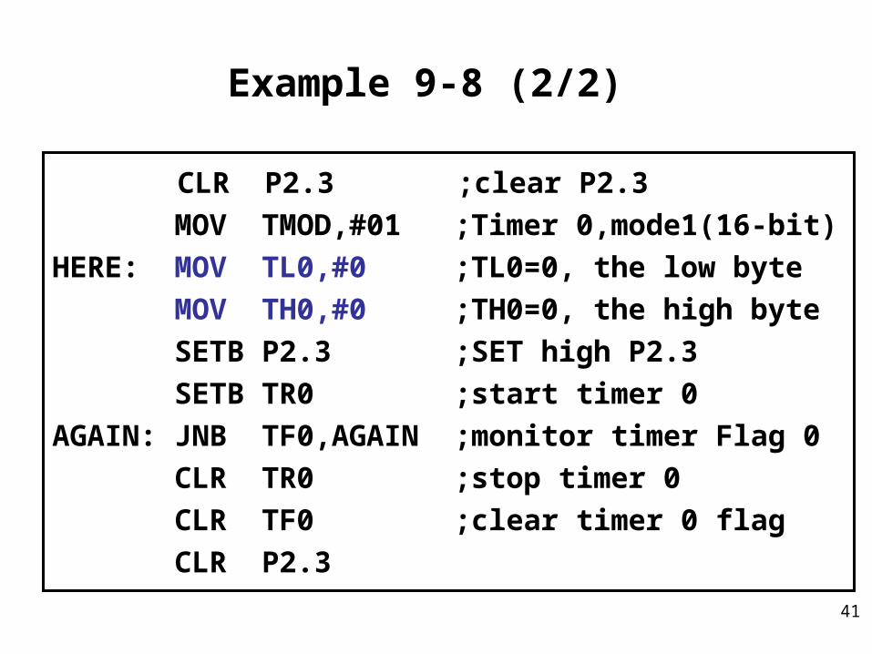
CLR P2.3 ;clear P2.3
MOV TMOD,#01 ;Timer 0,mode1(16-bit)
HERE: MOV TL0,#0 ;TL0=0, the low byte
MOV TH0,#0 ;TH0=0, the high byte
SETB P2.3 ;SET high P2.3
SETB TR0 ;start timer 0
AGAIN: JNB TF0,AGAIN ;monitor timer Flag 0
CLR TR0 ;stop timer 0
CLR TF0 ;clear timer 0 flag
CLR P2.3
42
Example 9-9 (1/2)
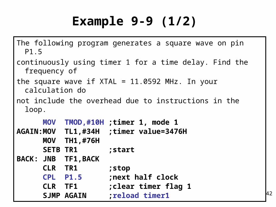
The following program generates a square wave on pin P1.5
continuously using timer 1 for a time delay. Find the frequency of
the square wave if XTAL = 11.0592 MHz. In your calculation do
not include the overhead due to instructions in the loop.
MOV TMOD,#10H ;timer 1, mode 1AGAIN:MOV TL1,#34H ;timer value=3476H MOV TH1,#76H SETB TR1 ;startBACK: JNB TF1,BACK CLR TR1 ;stop CPL P1.5 ;next half clock CLR TF1 ;clear timer flag 1 SJMP AGAIN ;reload timer1
43
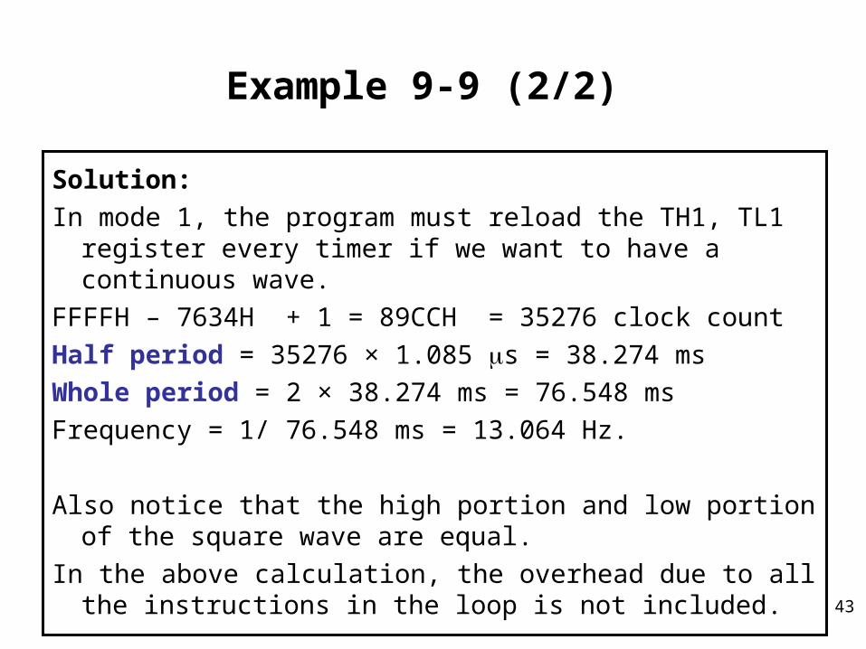
Example 9-9 (2/2)
Solution:
In mode 1, the program must reload the TH1, TL1 register every timer if we want to have a continuous wave.
FFFFH – 7634H + 1 = 89CCH = 35276 clock count
Half period = 35276 × 1.085 s = 38.274 ms
Whole period = 2 × 38.274 ms = 76.548 ms
Frequency = 1/ 76.548 ms = 13.064 Hz.
Also notice that the high portion and low portion of the square wave are equal.
In the above calculation, the overhead due to all the instructions in the loop is not included.
44
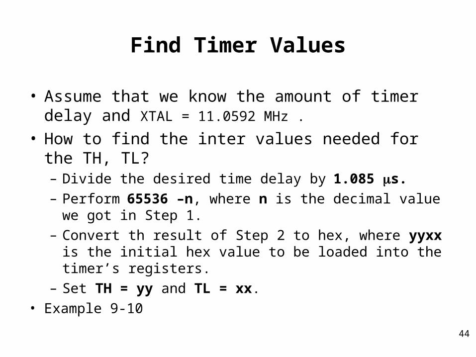
Find Timer Values
• Assume that we know the amount of timer delay and XTAL = 11.0592 MHz .
• How to find the inter values needed for the TH, TL?– Divide the desired time delay by 1.085 s.
– Perform 65536 –n, where n is the decimal value we got in Step 1.
– Convert th result of Step 2 to hex, where yyxx is the initial hex value to be loaded into the timer’s registers.
– Set TH = yy and TL = xx.
• Example 9-10
45
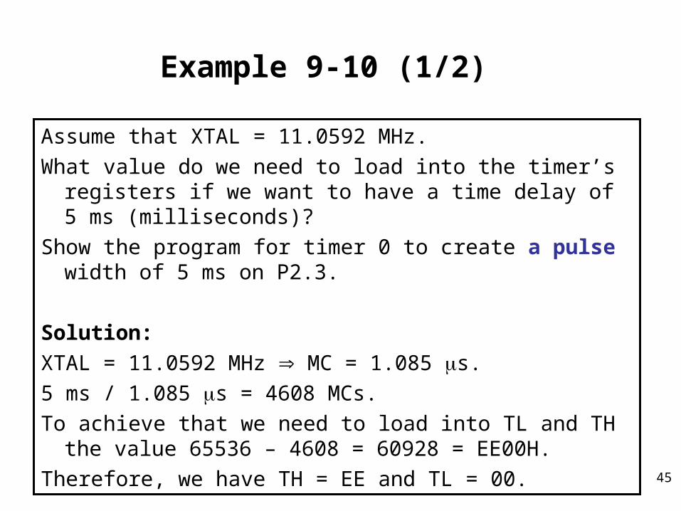
Example 9-10 (1/2)
Assume that XTAL = 11.0592 MHz.
What value do we need to load into the timer’s registers if we want to have a time delay of 5 ms (milliseconds)?
Show the program for timer 0 to create a pulse width of 5 ms on P2.3.
Solution:
XTAL = 11.0592 MHz MC = 1.085 s.
5 ms / 1.085 s = 4608 MCs.
To achieve that we need to load into TL and TH the value 65536 – 4608 = 60928 = EE00H.
Therefore, we have TH = EE and TL = 00.
46
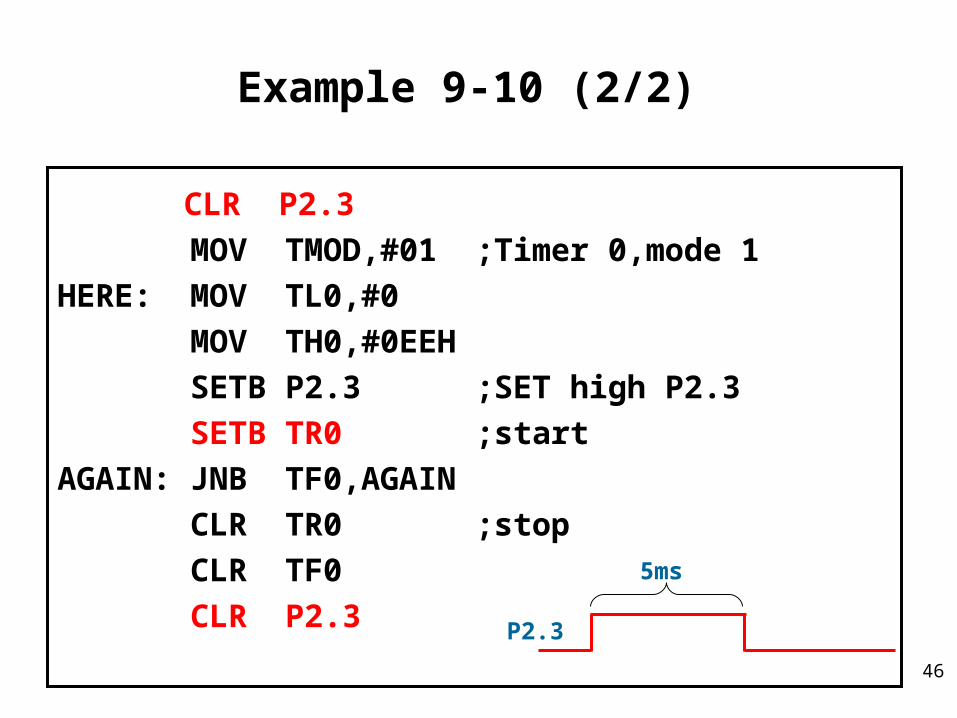
Example 9-10 (2/2)
CLR P2.3
MOV TMOD,#01 ;Timer 0,mode 1
HERE: MOV TL0,#0
MOV TH0,#0EEH
SETB P2.3 ;SET high P2.3
SETB TR0 ;start
AGAIN: JNB TF0,AGAIN
CLR TR0 ;stop
CLR TF0
CLR P2.3
P2.3
5ms
47
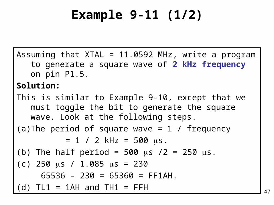
Example 9-11 (1/2)
Assuming that XTAL = 11.0592 MHz, write a program to generate a square wave of 2 kHz frequency on pin P1.5.
Solution:
This is similar to Example 9-10, except that we must toggle the bit to generate the square wave. Look at the following steps.
(a) The period of square wave = 1 / frequency
= 1 / 2 kHz = 500 s.
(b) The half period = 500 s /2 = 250 s.
(c) 250 s / 1.085 s = 230
65536 – 230 = 65360 = FF1AH.
(d) TL1 = 1AH and TH1 = FFH
48
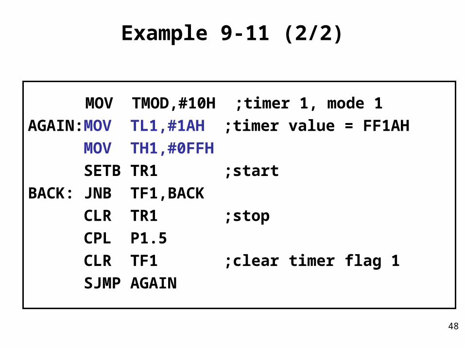
Example 9-11 (2/2)
MOV TMOD,#10H ;timer 1, mode 1
AGAIN:MOV TL1,#1AH ;timer value = FF1AH
MOV TH1,#0FFH
SETB TR1 ;start
BACK: JNB TF1,BACK
CLR TR1 ;stop
CPL P1.5
CLR TF1 ;clear timer flag 1
SJMP AGAIN
49
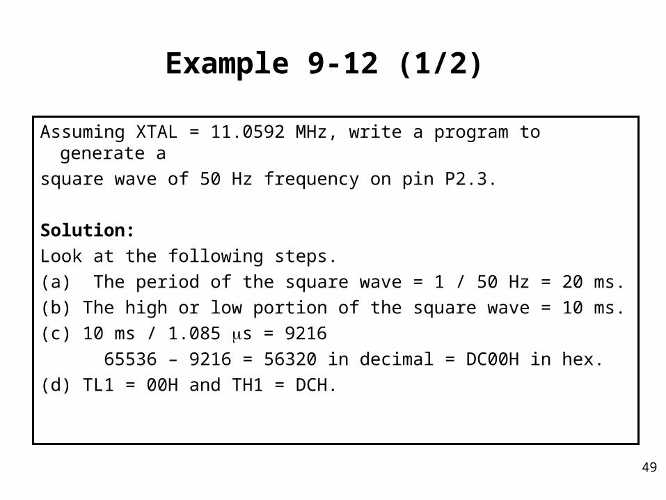
Example 9-12 (1/2)
Assuming XTAL = 11.0592 MHz, write a program to generate a
square wave of 50 Hz frequency on pin P2.3.
Solution:
Look at the following steps.
(a) The period of the square wave = 1 / 50 Hz = 20 ms.
(b) The high or low portion of the square wave = 10 ms.
(c) 10 ms / 1.085 s = 9216
65536 – 9216 = 56320 in decimal = DC00H in hex.
(d) TL1 = 00H and TH1 = DCH.
50
Example 9-12 (2/2)
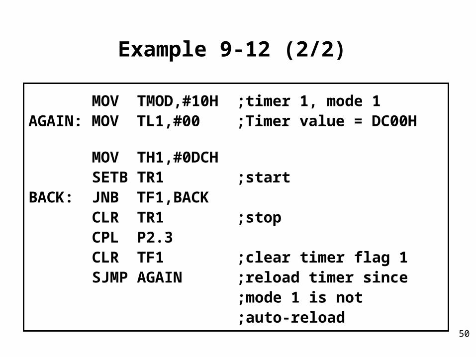
MOV TMOD,#10H ;timer 1, mode 1AGAIN: MOV TL1,#00 ;Timer value = DC00H
MOV TH1,#0DCH SETB TR1 ;startBACK: JNB TF1,BACK CLR TR1 ;stop CPL P2.3 CLR TF1 ;clear timer flag 1 SJMP AGAIN ;reload timer since ;mode 1 is not ;auto-reload
51
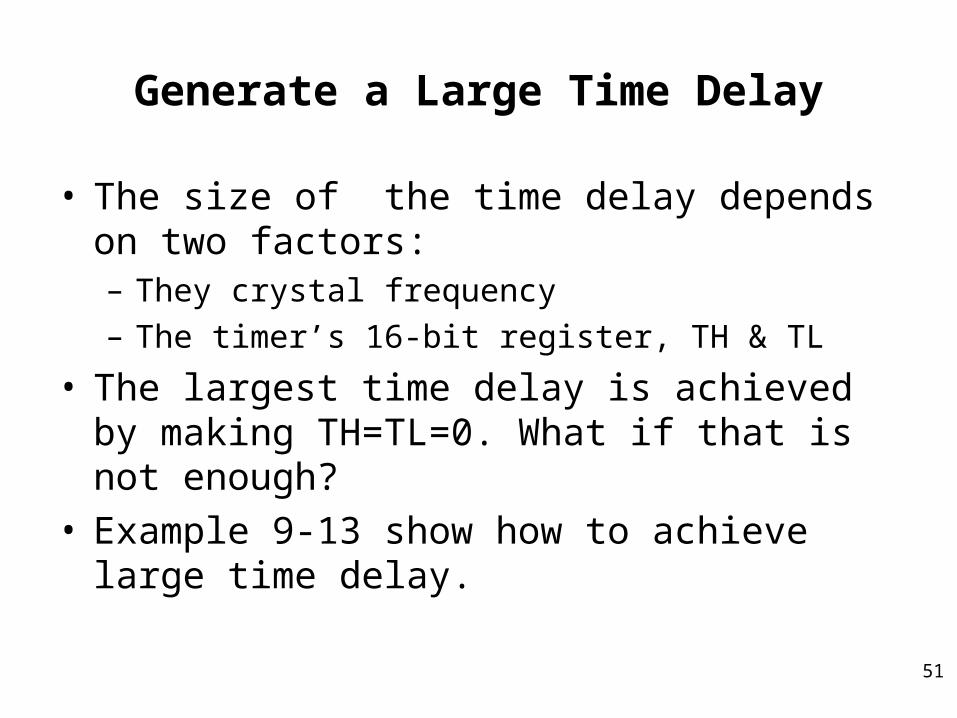
Generate a Large Time Delay
• The size of the time delay depends on two factors:– They crystal frequency
– The timer’s 16-bit register, TH & TL
• The largest time delay is achieved by making TH=TL=0. What if that is not enough?
• Example 9-13 show how to achieve large time delay.
52
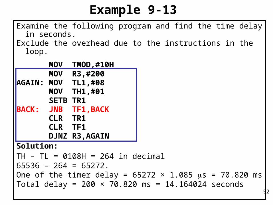
Example 9-13Examine the following program and find the time delay in seconds. Exclude the overhead due to the instructions in the loop.
MOV TMOD,#10H MOV R3,#200 AGAIN: MOV TL1,#08 MOV TH1,#01 SETB TR1 BACK: JNB TF1,BACK CLR TR1 CLR TF1 DJNZ R3,AGAIN Solution:TH – TL = 0108H = 264 in decimal 65536 – 264 = 65272.One of the timer delay = 65272 × 1.085 s = 70.820 msTotal delay = 200 × 70.820 ms = 14.164024 seconds
53
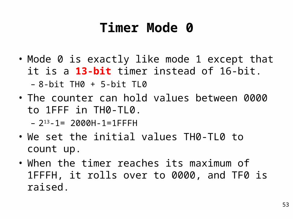
Timer Mode 0
• Mode 0 is exactly like mode 1 except that it is a 13-bit timer instead of 16-bit.– 8-bit TH0 + 5-bit TL0
• The counter can hold values between 0000 to 1FFF in TH0-TL0.– 213-1= 2000H-1=1FFFH
• We set the initial values TH0-TL0 to count up.• When the timer reaches its maximum of 1FFFH, it
rolls over to 0000, and TF0 is raised.
54
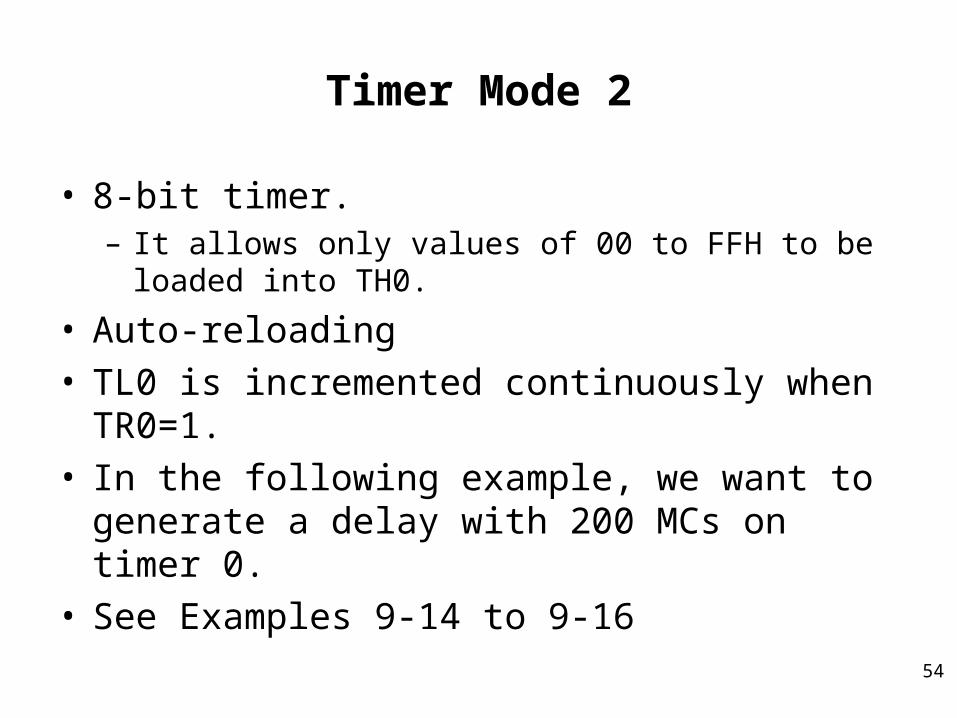
Timer Mode 2
• 8-bit timer. – It allows only values of 00 to FFH to be loaded into TH0.
• Auto-reloading• TL0 is incremented continuously when TR0=1.• In the following example, we want to generate a
delay with 200 MCs on timer 0.• See Examples 9-14 to 9-16
55
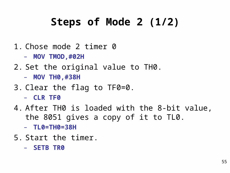
Steps of Mode 2 (1/2)
1. Chose mode 2 timer 0– MOV TMOD,#02H
2. Set the original value to TH0.– MOV TH0,#38H
3. Clear the flag to TF0=0.– CLR TF0
4. After TH0 is loaded with the 8-bit value, the 8051 gives a copy of it to TL0.– TL0=TH0=38H
5. Start the timer.– SETB TR0
56
Steps of Mode 2 (2/2)
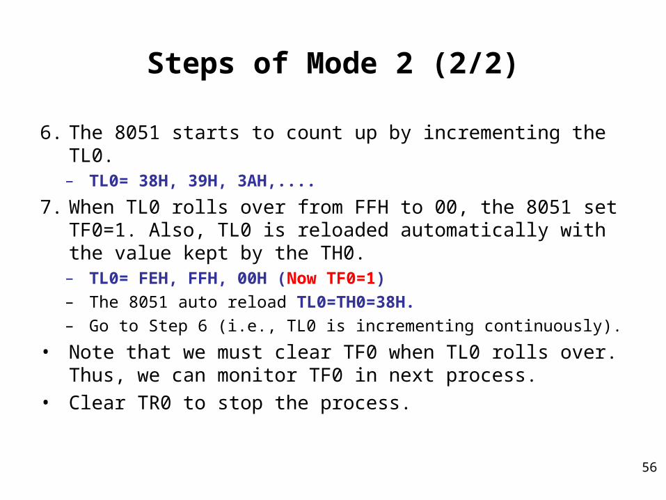
6. The 8051 starts to count up by incrementing the TL0.– TL0= 38H, 39H, 3AH,....
7. When TL0 rolls over from FFH to 00, the 8051 set TF0=1. Also, TL0 is reloaded automatically with the value kept by the TH0.– TL0= FEH, FFH, 00H (Now TF0=1)– The 8051 auto reload TL0=TH0=38H. – Go to Step 6 (i.e., TL0 is incrementing continuously).
• Note that we must clear TF0 when TL0 rolls over. Thus, we can monitor TF0 in next process.
• Clear TR0 to stop the process.
57
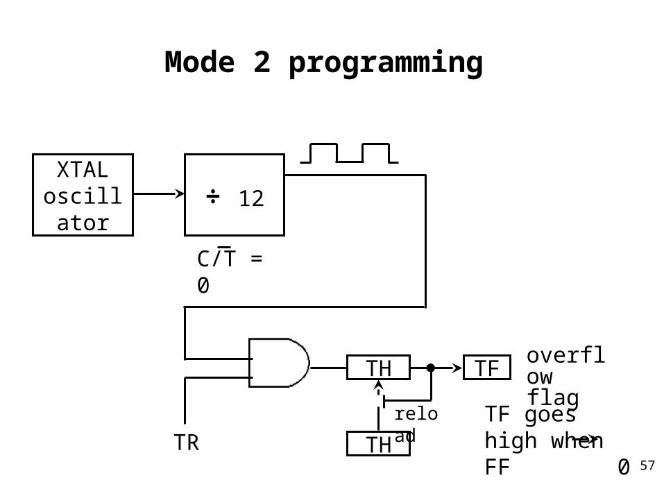
Mode 2 programming
XTALoscillator ÷ 12
TR
TH
TH
TF
TF goes high when FF 0
overflow flag
C/T = 0
reload
58
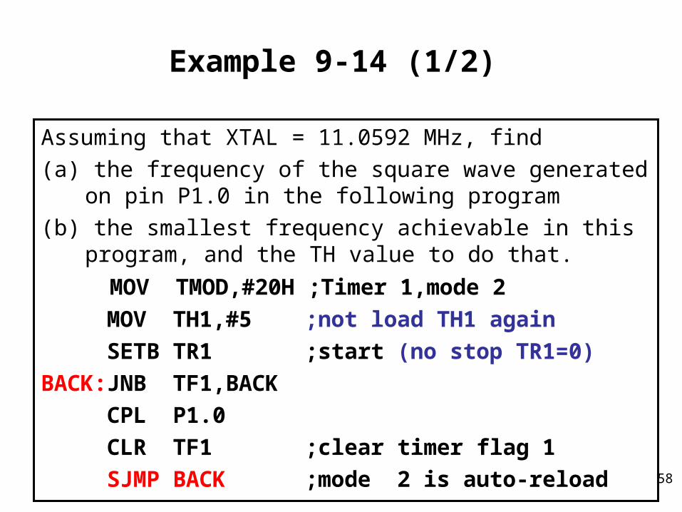
Example 9-14 (1/2)
Assuming that XTAL = 11.0592 MHz, find
(a) the frequency of the square wave generated on pin P1.0 in the following program
(b) the smallest frequency achievable in this program, and the TH value to do that.
MOV TMOD,#20H ;Timer 1,mode 2 MOV TH1,#5 ;not load TH1 again
SETB TR1 ;start (no stop TR1=0)
BACK:JNB TF1,BACK
CPL P1.0
CLR TF1 ;clear timer flag 1
SJMP BACK ;mode 2 is auto-reload
59
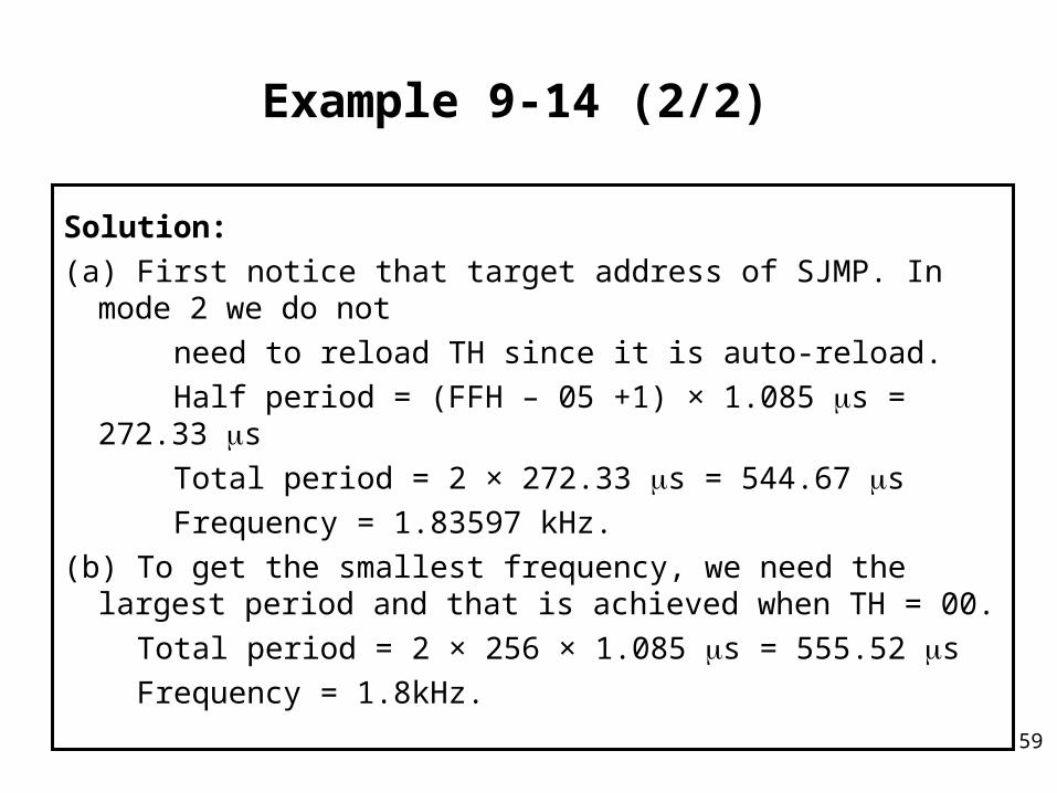
Example 9-14 (2/2)
Solution:
(a) First notice that target address of SJMP. In mode 2 we do not
need to reload TH since it is auto-reload.
Half period = (FFH – 05 +1) × 1.085 s = 272.33 s
Total period = 2 × 272.33 s = 544.67 s
Frequency = 1.83597 kHz.
(b) To get the smallest frequency, we need the largest period and that is achieved when TH = 00.
Total period = 2 × 256 × 1.085 s = 555.52 s
Frequency = 1.8kHz.
60
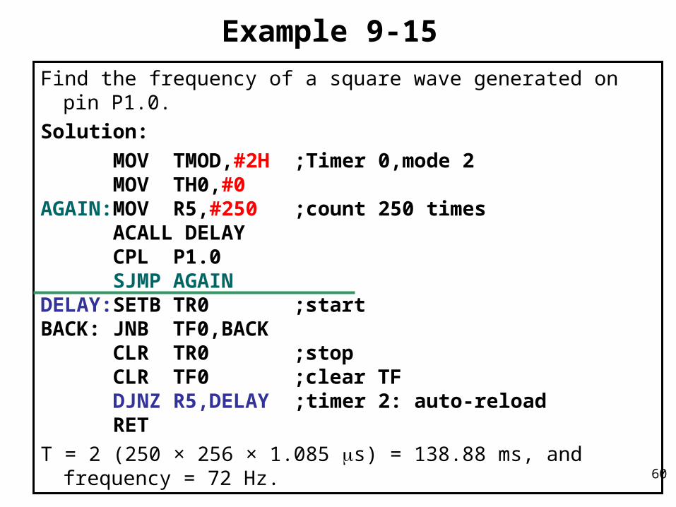
Example 9-15
Find the frequency of a square wave generated on pin P1.0.
Solution:
MOV TMOD,#2H ;Timer 0,mode 2 MOV TH0,#0 AGAIN:MOV R5,#250 ;count 250 times ACALL DELAY CPL P1.0 SJMP AGAINDELAY:SETB TR0 ;startBACK: JNB TF0,BACK CLR TR0 ;stop CLR TF0 ;clear TF DJNZ R5,DELAY ;timer 2: auto-reload RET
T = 2 (250 × 256 × 1.085 s) = 138.88 ms, and frequency = 72 Hz.
61
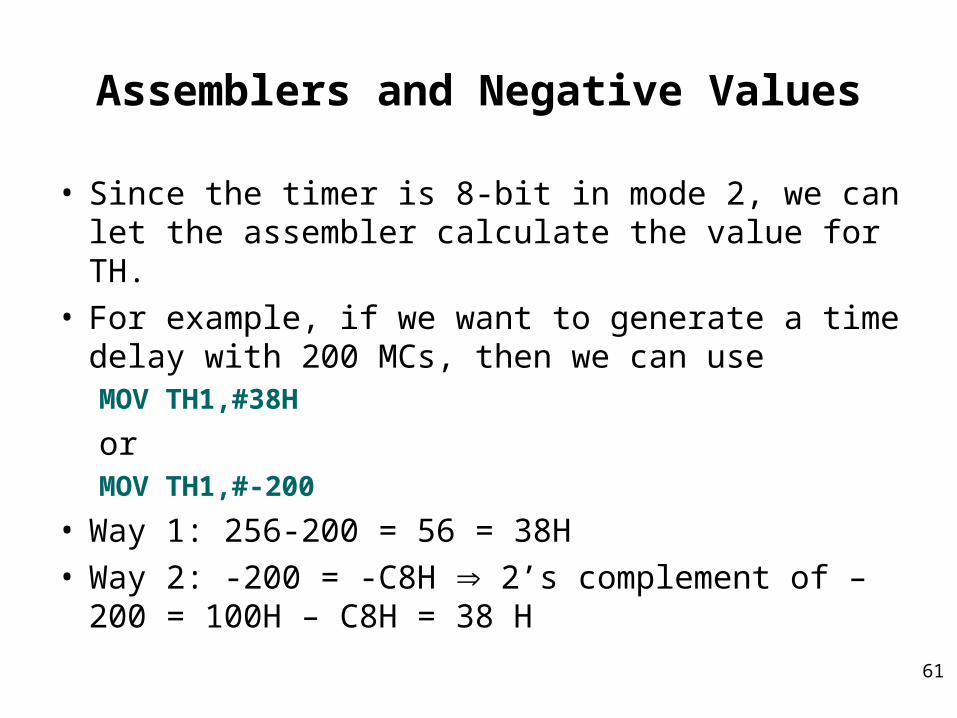
Assemblers and Negative Values
• Since the timer is 8-bit in mode 2, we can let the assembler calculate the value for TH.
• For example, if we want to generate a time delay with 200 MCs, then we can use MOV TH1,#38H
orMOV TH1,#-200
• Way 1: 256-200 = 56 = 38H• Way 2: -200 = -C8H 2’s complement of –200 =
100H – C8H = 38 H
62
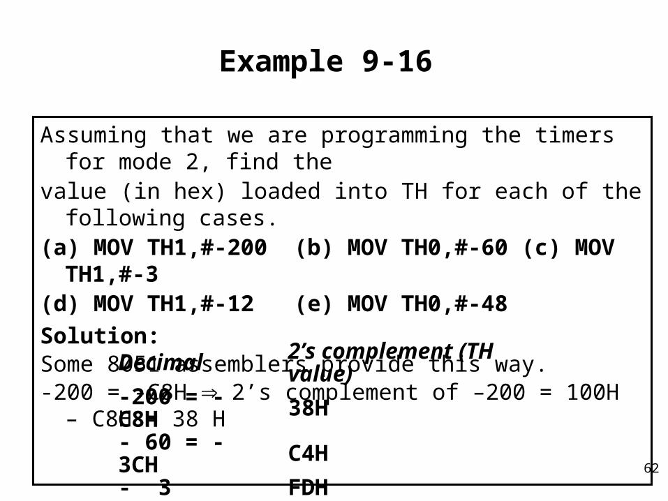
Example 9-16
Assuming that we are programming the timers for mode 2, find the value (in hex) loaded into TH for each of the following cases.(a) MOV TH1,#-200 (b) MOV TH0,#-60 (c) MOV TH1,#-3(d) MOV TH1,#-12 (e) MOV TH0,#-48
Solution:Some 8051 assemblers provide this way.-200 = -C8H 2’s complement of –200 = 100H – C8H = 38 H
Decimal 2’s complement (TH value)-200 = - C8H 38H- 60 = - 3CH C4H- 3 FDH- 12 F4H- 48 D0H
63
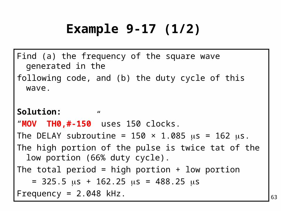
Example 9-17 (1/2)
Find (a) the frequency of the square wave generated in the
following code, and (b) the duty cycle of this wave.
Solution:
“MOV TH0,#-150” uses 150 clocks.
The DELAY subroutine = 150 × 1.085 s = 162 s.
The high portion of the pulse is twice tat of the low portion (66% duty cycle).
The total period = high portion + low portion
= 325.5 s + 162.25 s = 488.25 s
Frequency = 2.048 kHz.
64
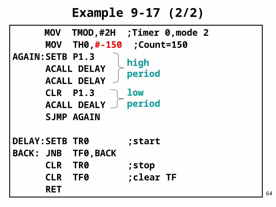
Example 9-17 (2/2)
MOV TMOD,#2H ;Timer 0,mode 2 MOV TH0,#-150 ;Count=150AGAIN:SETB P1.3 ACALL DELAY ACALL DELAY CLR P1.3 ACALL DEALY SJMP AGAIN
DELAY:SETB TR0 ;startBACK: JNB TF0,BACK CLR TR0 ;stop CLR TF0 ;clear TF RET
high period
low period
65
Section 9.2Counter Programming
66
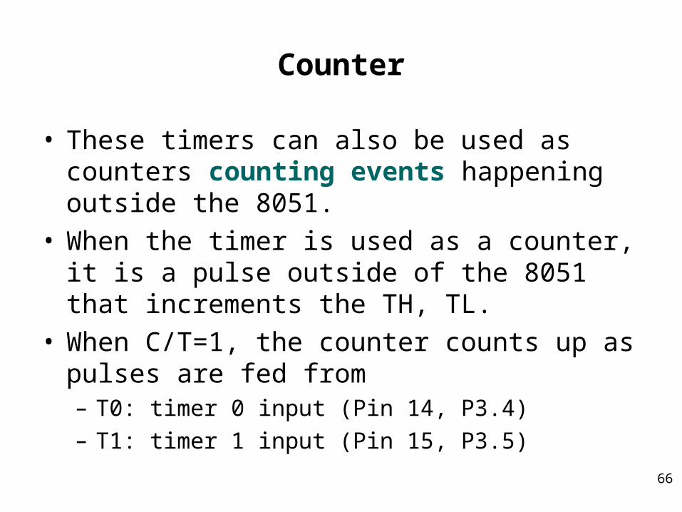
Counter
• These timers can also be used as counters counting events happening outside the 8051.
• When the timer is used as a counter, it is a pulse outside of the 8051 that increments the TH, TL.
• When C/T=1, the counter counts up as pulses are fed from– T0: timer 0 input (Pin 14, P3.4)
– T1: timer 1 input (Pin 15, P3.5)
67
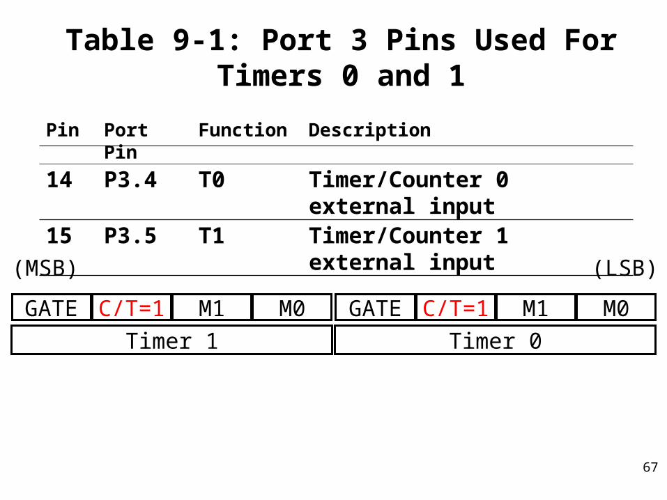
Table 9-1: Port 3 Pins Used For Timers 0 and 1
Pin Port Pin Function Description
14 P3.4 T0 Timer/Counter 0 external input15 P3.5 T1 Timer/Counter 1 external input
GATE C/T=1 M1 M0 GATE C/T=1 M1 M0
Timer 1 Timer 0
(MSB) (LSB)
68
Counter Mode 1
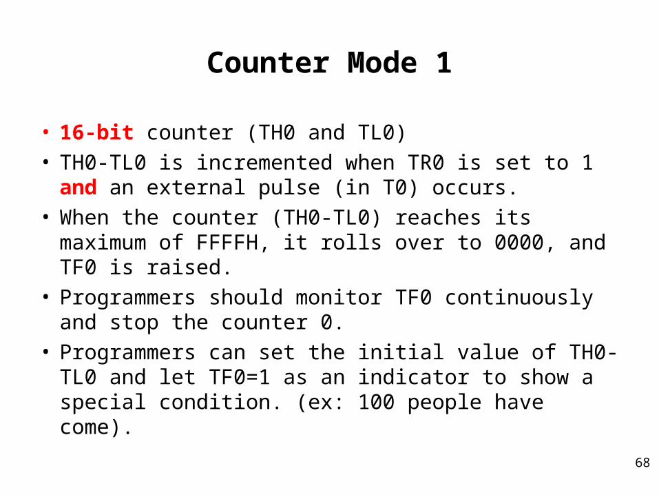
• 16-bit counter (TH0 and TL0)• TH0-TL0 is incremented when TR0 is set to 1 and an
external pulse (in T0) occurs.• When the counter (TH0-TL0) reaches its maximum
of FFFFH, it rolls over to 0000, and TF0 is raised.• Programmers should monitor TF0 continuously and
stop the counter 0.• Programmers can set the initial value of TH0-TL0
and let TF0=1 as an indicator to show a special condition. (ex: 100 people have come).
69
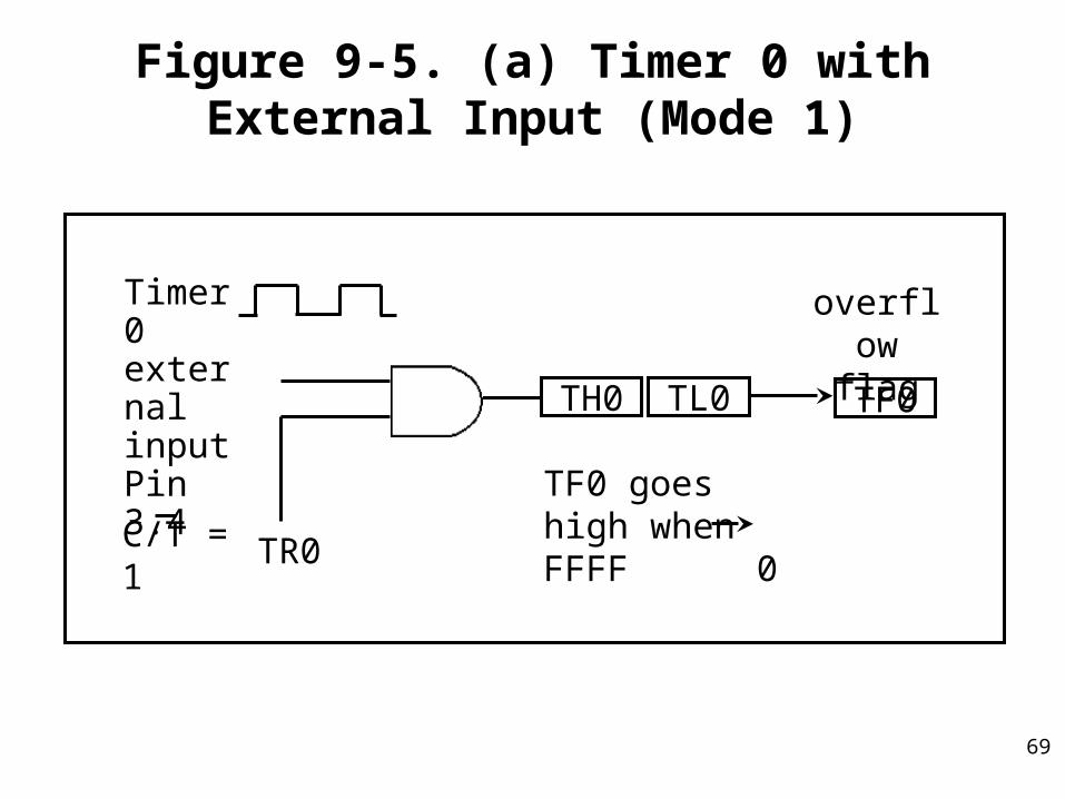
Figure 9-5. (a) Timer 0 with External Input (Mode 1)
Timer 0 external input Pin 3.4
TR0
TH0 TL0 TF0
TF0 goes high when FFFF 0
overflow flag
C/T = 1

70
Figure 9-5. (b) Timer 1 with External Input (Mode 1)
Timer 1 external input Pin 3.5
TR1
TH1 TL1 TF1
TF1 goes high when FFFF 0
overflow flag
C/T = 1
71
Counter Mode 2
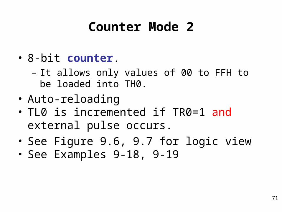
• 8-bit counter. – It allows only values of 00 to FFH to be loaded into TH0.
• Auto-reloading• TL0 is incremented if TR0=1 and external pulse
occurs.• See Figure 9.6, 9.7 for logic view• See Examples 9-18, 9-19
72
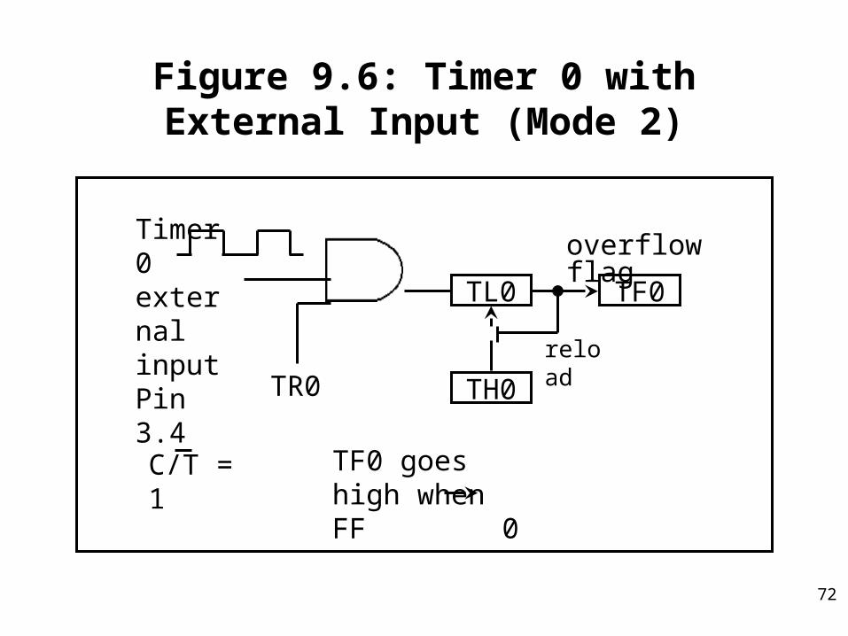
Figure 9.6: Timer 0 with External Input (Mode 2)
Timer 0 external input Pin 3.4 TR0
TL0
TH0
TF0
TF0 goes high when FF 0
overflow flag
C/T = 1
reload
73
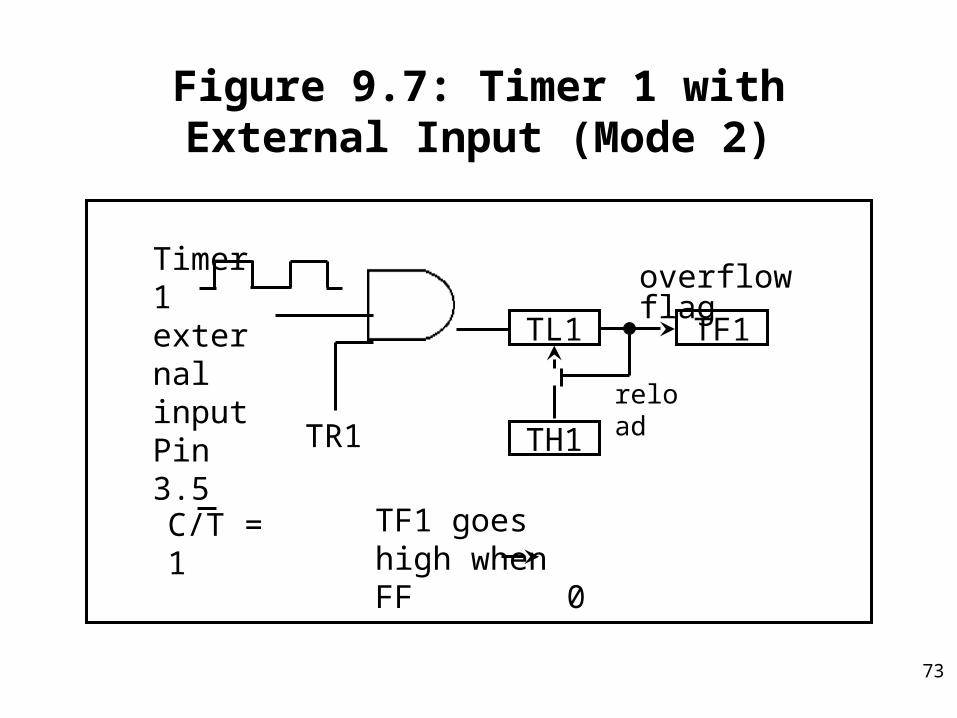
Figure 9.7: Timer 1 with External Input (Mode 2)
Timer 1 external input Pin 3.5 TR1
TL1
TH1
TF1
TF1 goes high when FF 0
overflow flag
C/T = 1
reload
74
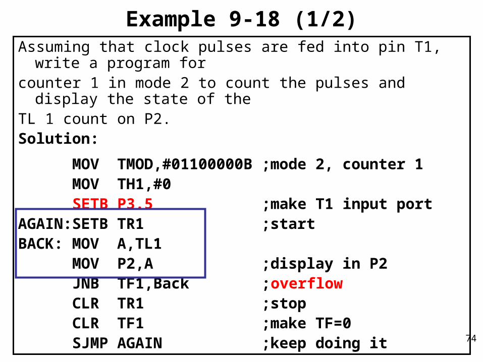
Example 9-18 (1/2)Assuming that clock pulses are fed into pin T1, write a program for counter 1 in mode 2 to count the pulses and display the state of the TL 1 count on P2.Solution:
MOV TMOD,#01100000B ;mode 2, counter 1 MOV TH1,#0 SETB P3.5 ;make T1 input portAGAIN:SETB TR1 ;startBACK: MOV A,TL1 MOV P2,A ;display in P2 JNB TF1,Back ;overflow CLR TR1 ;stop CLR TF1 ;make TF=0 SJMP AGAIN ;keep doing it
75
Example 9-18 (2/2)
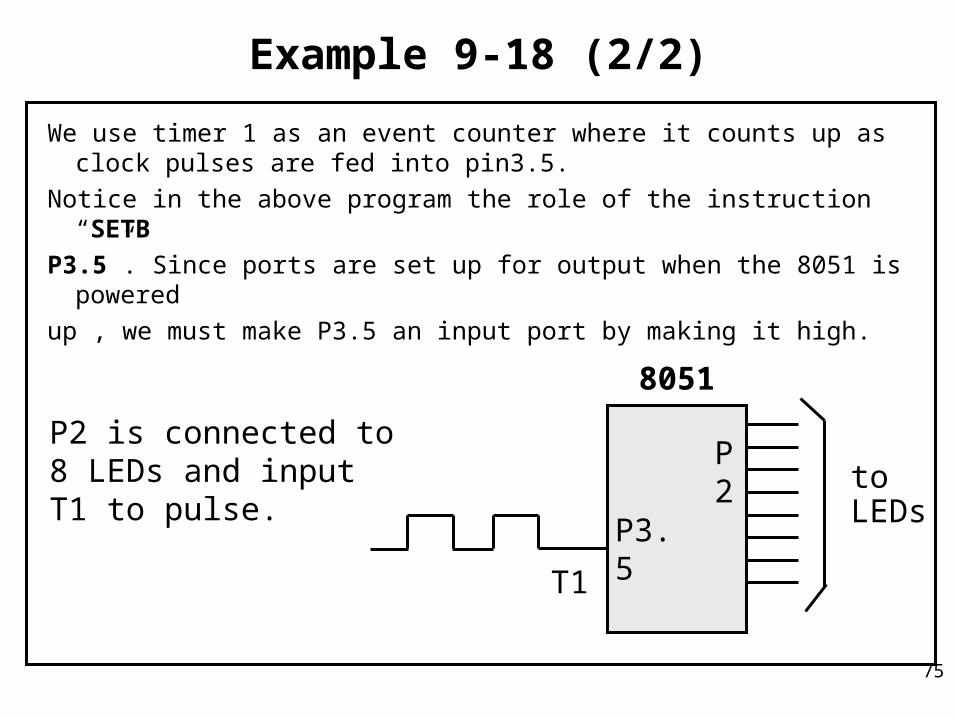
We use timer 1 as an event counter where it counts up as clock pulses are fed into pin3.5.
Notice in the above program the role of the instruction “SETB
P3.5”. Since ports are set up for output when the 8051 is powered
up , we must make P3.5 an input port by making it high.
P2 is connected to 8 LEDs and input T1 to pulse.
T1
toLEDs
P3.5
P2
8051
76
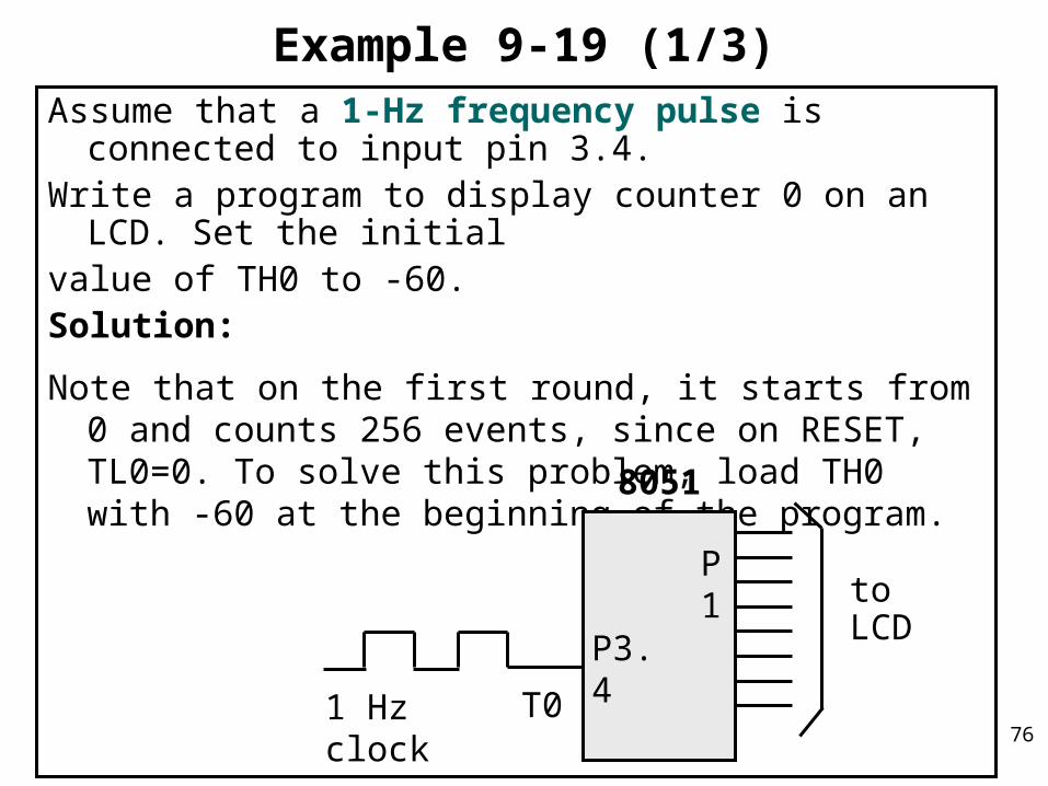
Example 9-19 (1/3)Assume that a 1-Hz frequency pulse is connected to input pin 3.4. Write a program to display counter 0 on an LCD. Set the initial value of TH0 to -60.Solution:
Note that on the first round, it starts from 0 and counts 256 events, since on RESET, TL0=0. To solve this problem, load TH0 with -60 at the beginning of the program.
T0
toLCD
P3.4
P1
8051
1 Hz clock
77
Example 9-19 (2/3)
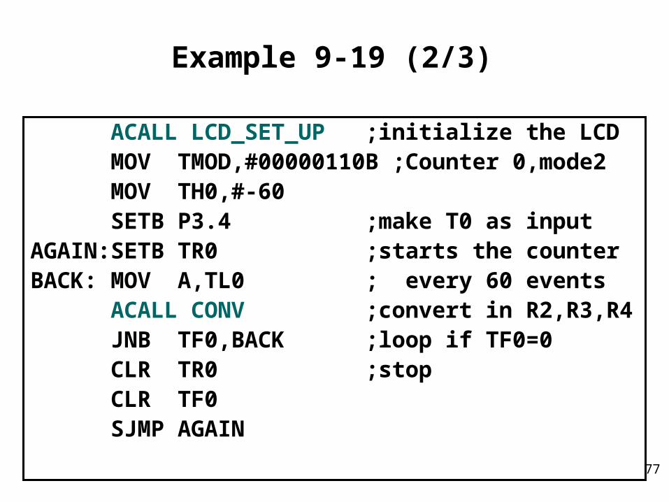
ACALL LCD_SET_UP ;initialize the LCD MOV TMOD,#00000110B ;Counter 0,mode2 MOV TH0,#-60 SETB P3.4 ;make T0 as inputAGAIN:SETB TR0 ;starts the counterBACK: MOV A,TL0 ; every 60 events ACALL CONV ;convert in R2,R3,R4 JNB TF0,BACK ;loop if TF0=0 CLR TR0 ;stop CLR TF0 SJMP AGAIN
78
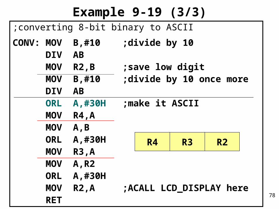
Example 9-19 (3/3);converting 8-bit binary to ASCII
CONV: MOV B,#10 ;divide by 10 DIV AB MOV R2,B ;save low digit MOV B,#10 ;divide by 10 once more DIV AB ORL A,#30H ;make it ASCII MOV R4,A MOV A,B ORL A,#30H MOV R3,A MOV A,R2 ORL A,#30H MOV R2,A ;ACALL LCD_DISPLAY here RET
R4 R3 R2
79
A Digital Clock
• Example 9-19 shows a simple digital clock.– If we feed an external square wave of 60 Hz frequency into
the timer/counter, we can generate the second, the minute, and the hour out of this input frequency and display the result on an LCD.
• You might think that the use of the instruction “JNB TF0,target” to monitor the raising of the TF0 flag is a waste of the microcontroller’s time.– The solution is the use of interrupt. See Chapter 11.
– In using interrupts we can do other things with the 8051.
– When the TF flag is raised it will inform us.
80
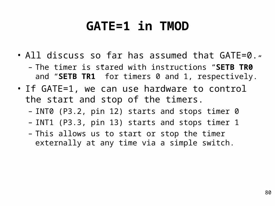
GATE=1 in TMOD
• All discuss so far has assumed that GATE=0.– The timer is stared with instructions “SETB TR0” and
“SETB TR1” for timers 0 and 1, respectively.
• If GATE=1, we can use hardware to control the start and stop of the timers.– INT0 (P3.2, pin 12) starts and stops timer 0
– INT1 (P3.3, pin 13) starts and stops timer 1
– This allows us to start or stop the timer externally at any time via a simple switch.
81
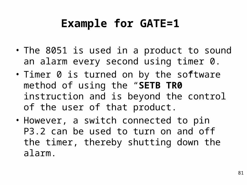
Example for GATE=1
• The 8051 is used in a product to sound an alarm every second using timer 0.
• Timer 0 is turned on by the software method of using the “SETB TR0” instruction and is beyond the control of the user of that product.
• However, a switch connected to pin P3.2 can be used to turn on and off the timer, thereby shutting down the alarm.
82
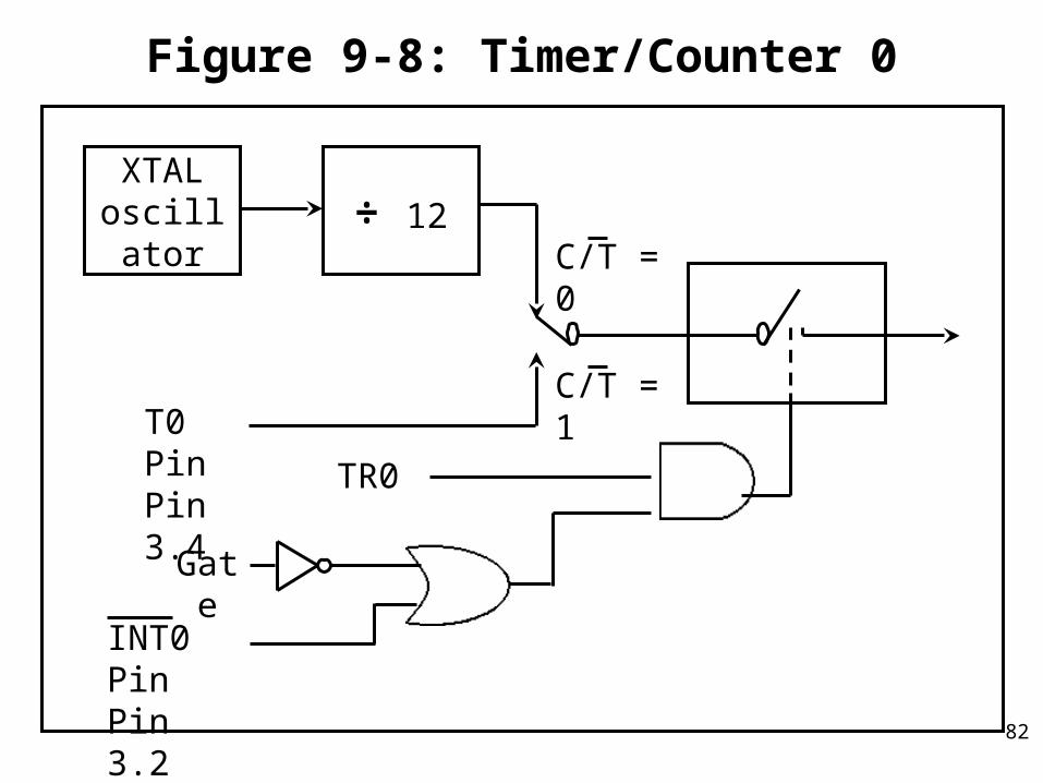
Figure 9-8: Timer/Counter 0
XTALoscillator ÷ 12
TR0
INT0 Pin Pin 3.2
C/T = 0
Gate
T0 Pin Pin 3.4
C/T = 1
83
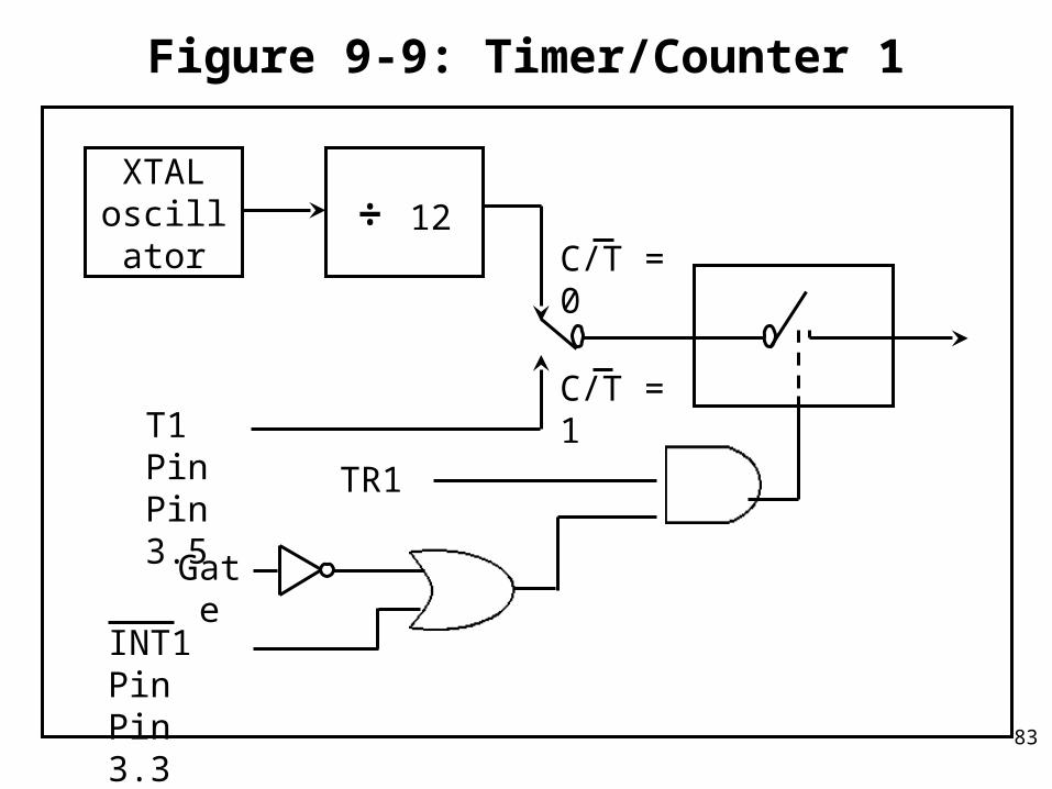
Figure 9-9: Timer/Counter 1
XTALoscillator ÷ 12
TR1
INT1 Pin Pin 3.3
C/T = 0
Gate
T1 Pin Pin 3.5
C/T = 1
84
Timer/Counter Mode 3
• For Timer/Counter 0– As a Timer:
• Two 8-bit timers
– As a Counter:• 8-bit counter.
• For Timer/Counter 1– Not available

85
86
You are able to
• List the timers of the 8051 and their associated registers
• Describe the various modes of the 8051 timers• Program the 8051 timers to generate time delays• Program the 8051 counters as event counters
87
Homework
• Chapter 9 Problems : 9,20,22,26,31,36,44,47,48