Embed Size (px)
Citation preview
1
High Voltage Power IC
설계 기술
2010. 12. 9
박 시 홍
단국대학교 전자전기공학부
2목 차
- 고전압 파워 IC
- 고전압 파워 IC 공정 소개
- 고전압 파워 IC 설계 고려 사항

3
고전압 파워 IC
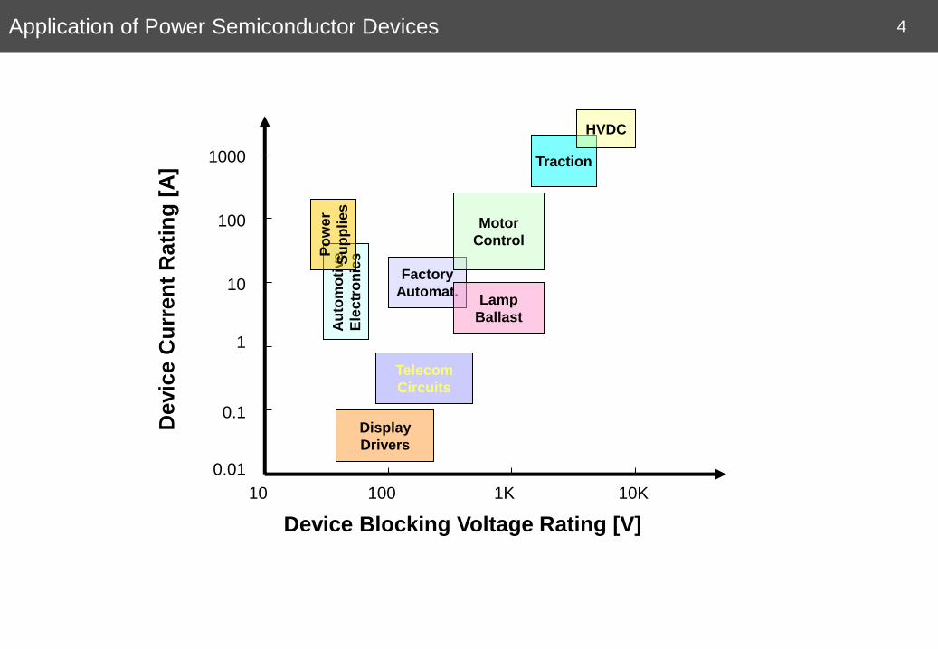
Application of Power Semiconductor Devices
10 100 1K 10K
0.01
0.1
1
10
100
1000
Display
Drivers
Telecom
Circuits
Au
tom
oti
ve
Ele
ctr
on
icsP
ow
er
Su
pp
lie
s
Factory
Automat.Lamp
Ballast
Motor
Control
Device Blocking Voltage Rating [V]
Devic
e C
urr
en
t R
ati
ng
[A
] Traction
HVDC
4
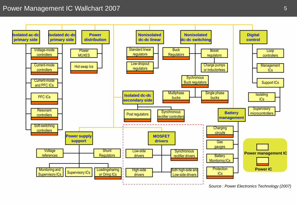
Power Management IC Wallchart 2007
Isolated ac-dc
primary side
Isolated dc-dc
primary side
Power
distribution
Nonisolated
dc-dc linear
Digital
control
Nonisolated
dc-dc switching
Power management IC
Power IC
Source : Power Electronics Technology (2007)
Voltage-mode
controllers
Current-mode
controllers
Current-mode
and PFC ICs
PFC ICs
Resonant
controllers
Soft-switching
controllers
Power
MUXES
Hot swap Ics
Power supply
support
Monitoring and
Supervisory ICs
Voltage
references
Shunt
Regulators
Supervisory ICsLoadingsharing
or Oring ICs
Isolated dc-dc
secondary side
Post regulatorsSynchronous
rectifier controllers
MOSFET
drivers
Low-side
drivers
High-side
drivers
Both high-side and
Low-side drivers
Synchronous
rectifier drivers
Low-dropout
regulators
Standard linear
regulators
Multiphase
bucks
Buck
RegulatorsBoost
regulators
Charge pumps
or inductorless
Sychronous
Buck regulators
Single phase
bucks
Battery
management
Charging
circuits
Gas
gauges
Battery
Monitoring ICs
Protection
ICs
Loop
controllers
Management
ICs
Support ICs
Isolating
ICs
Supervisory
microcontrollers
5
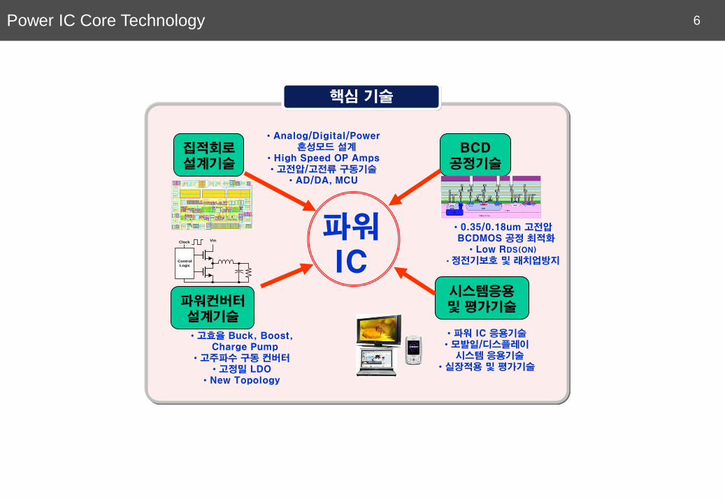
핵심 기술
BCD공정기술
파워컨버터설계기술
시스템응용및 평가기술
집적회로설계기술
• 0.35/0.18um 고전압BCDMOS 공정 최적화
• Low RDS(ON)
• 정전기보호 및 래치업방지
• 고효율 Buck, Boost,Charge Pump
• 고주파수 구동 컨버터• 고정밀 LDO
• New Topology
• Analog/Digital/Power 혼성모드 설계
• High Speed OP Amps• 고전압/고전류 구동기술
• AD/DA, MCU
• 파워 IC 응용기술• 모발일/디스플레이
시스템 응용기술• 실장적용 및 평가기술
파워ICControl
Logic
VinClock
Power IC Core Technology 6
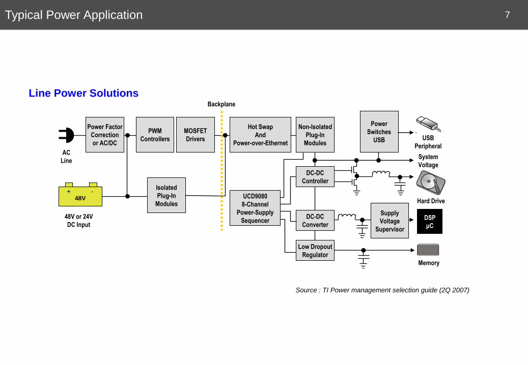
Typical Power Application
Source : TI Power management selection guide (2Q 2007)
Power Factor
Correction
or AC/DC
PWM
Controllers
MOSFET
Drivers
Hot Swap
And
Power-over-Ethernet
Non-Isolated
Plug-In
Modules
Power
Switches
USB
DC-DC
Controller
DC-DC
Converter
Low Dropout
Regulator
Isolated
Plug-In
Modules
Supply
Voltage
Supervisor
UCD9080
8-Channel
Power-Supply
Sequencer
+ -48V
Line Power Solutions
AC
Line
48V or 24V
DC Input
System
Voltage
USB
Peripheral
Hard Drive
DSP
μC
Memory
Backplane
7
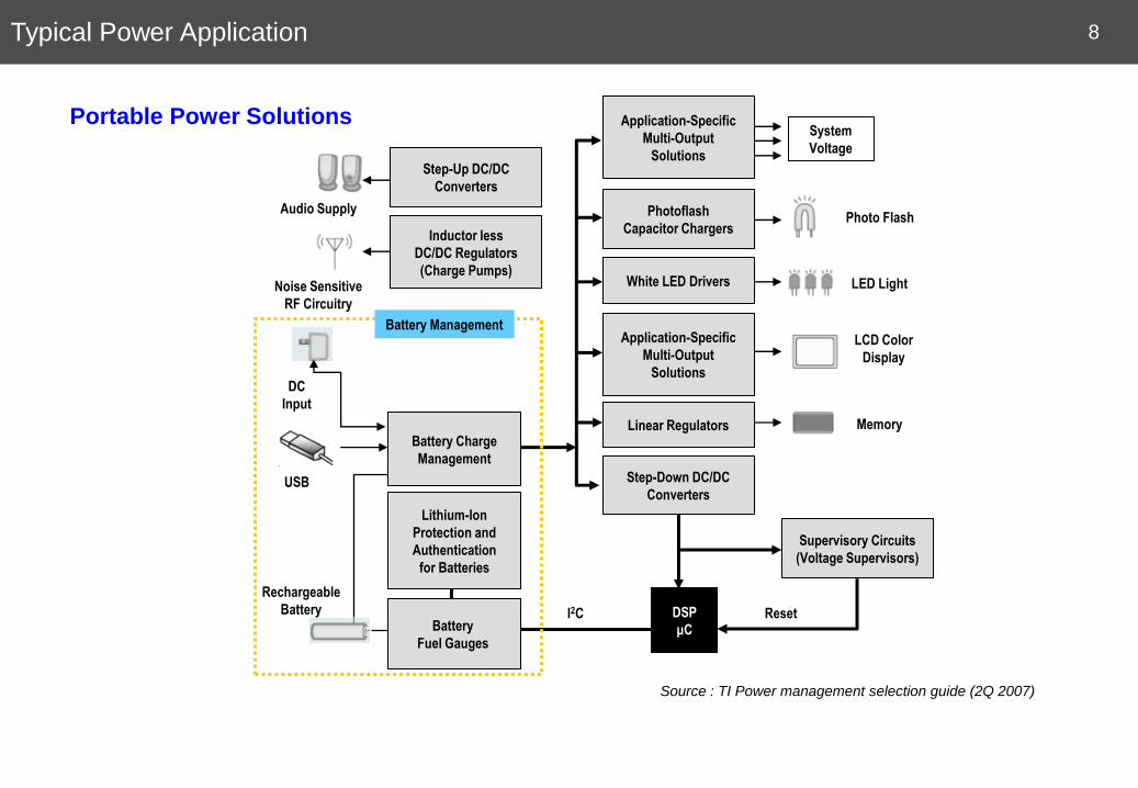
Step-Up DC/DC
Converters
Inductor less
DC/DC Regulators
(Charge Pumps)
Application-Specific
Multi-Output
Solutions
Photoflash
Capacitor Chargers
Linear Regulators
Application-Specific
Multi-Output
Solutions
White LED Drivers
Step-Down DC/DC
Converters
Supervisory Circuits
(Voltage Supervisors)
Battery Charge
Management
Lithium-Ion
Protection and
Authentication
for Batteries
Battery
Fuel Gauges
Portable Power Solutions
DSP
μC
System
Voltage
Photo Flash
LED Light
LCD Color
Display
Memory
ResetI2C
Audio Supply
Noise Sensitive
RF Circuitry
Battery Management
USB
DC
Input
Rechargeable
Battery
Source : TI Power management selection guide (2Q 2007)
Typical Power Application 8

9
고전압 파워 IC 공정
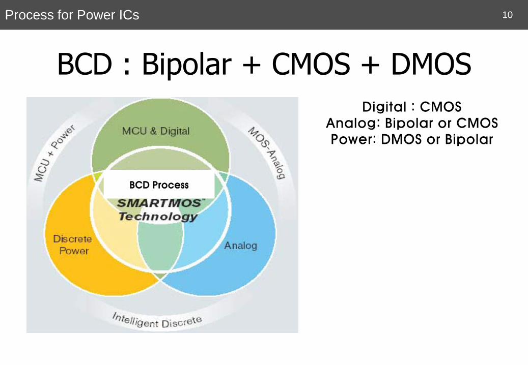
BCD : Bipolar + CMOS + DMOS
BCD Process
Digital : CMOSAnalog: Bipolar or CMOSPower: DMOS or Bipolar
Process for Power ICs 10
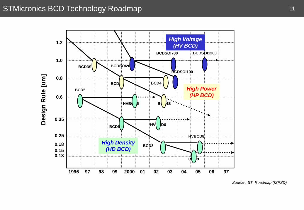
Desig
n R
ule
[u
m]
070605049998971996 0302012000
0.130.15
0.18
0.25
0.35
0.6
0.8
1.0
1.2
BCD5
HVBCD6 BCD6
BCD8
HVBCD8
BCD9
HVBCD5 BCD4S
High Density
(HD BCD)
BCD3S
BCD4 BCD4 SOI
BCDSOI200
High Power
(HP BCD)
BCDSOI700 BCDSOI1200
BCDSOI100
High Voltage
(HV BCD)
Source : ST Roadmap (ISPSD)
STMicronics BCD Technology Roadmap 11
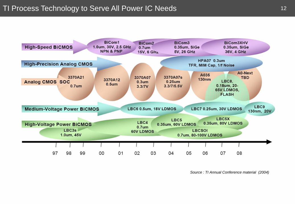
Source : TI Annual Conference material (2004)
TI Process Technology to Serve All Power IC Needs 12
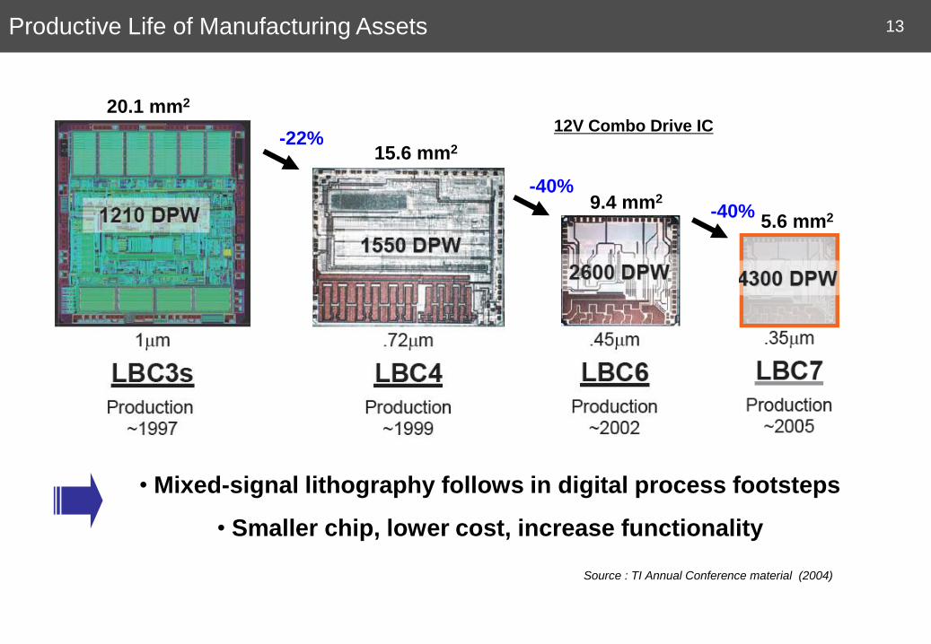
12V Combo Drive IC
• Mixed-signal lithography follows in digital process footsteps
• Smaller chip, lower cost, increase functionality
-22%
-40%
-40%
Source : TI Annual Conference material (2004)
20.1 mm2
15.6 mm2
9.4 mm2
5.6 mm2
Productive Life of Manufacturing Assets 13
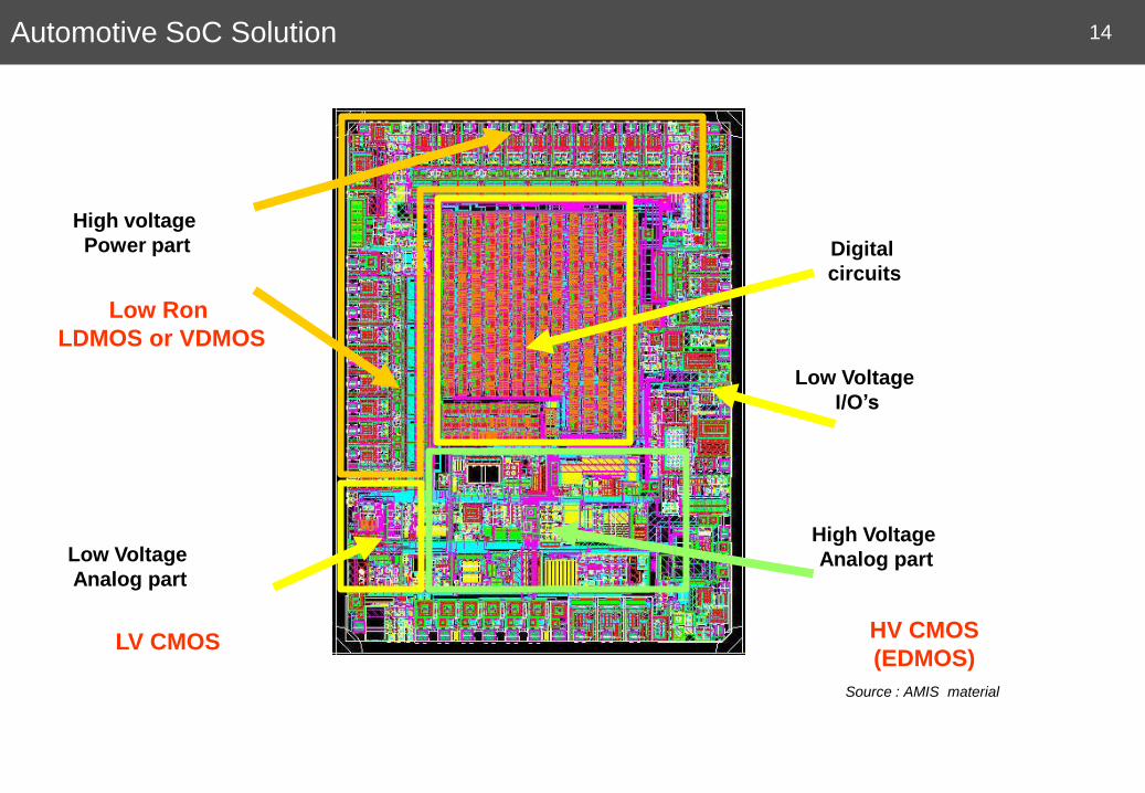
Source : AMIS material
High Voltage
Analog part
Digital
circuits
Low Voltage
Analog part
Low Voltage
I/O’s
High voltage
Power part
Low Ron
LDMOS or VDMOS
HV CMOS
(EDMOS)
Automotive SoC Solution
LV CMOS
14
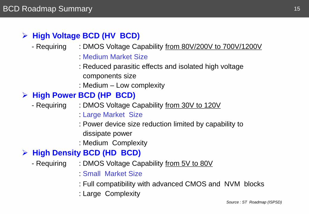
BCD Roadmap Summary
Source : ST Roadmap (ISPSD)
High Voltage BCD (HV BCD)
- Requiring : DMOS Voltage Capability from 80V/200V to 700V/1200V
: Medium Market Size
: Reduced parasitic effects and isolated high voltage
components size
: Medium – Low complexity
High Power BCD (HP BCD)
- Requiring : DMOS Voltage Capability from 30V to 120V
: Large Market Size
: Power device size reduction limited by capability to
dissipate power
: Medium Complexity
High Density BCD (HD BCD)
- Requiring : DMOS Voltage Capability from 5V to 80V
: Small Market Size
: Full compatibility with advanced CMOS and NVM blocks
: Large Complexity
15
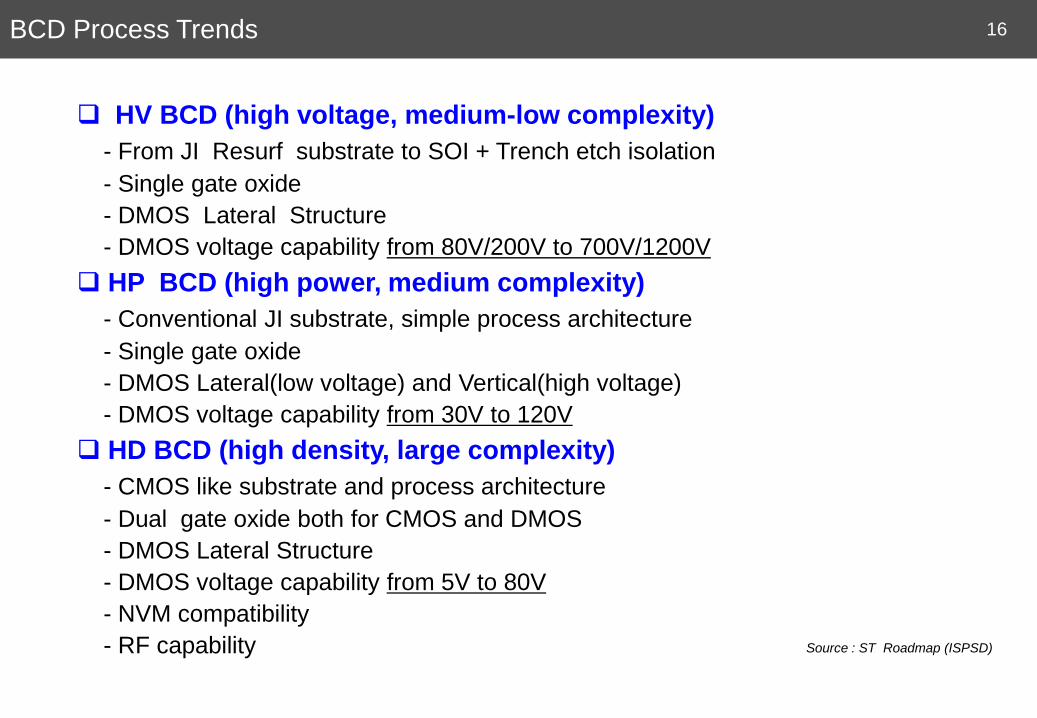
BCD Process Trends
Source : ST Roadmap (ISPSD)
HV BCD (high voltage, medium-low complexity)
- From JI Resurf substrate to SOI + Trench etch isolation
- Single gate oxide
- DMOS Lateral Structure
- DMOS voltage capability from 80V/200V to 700V/1200V
HP BCD (high power, medium complexity)
- Conventional JI substrate, simple process architecture
- Single gate oxide
- DMOS Lateral(low voltage) and Vertical(high voltage)
- DMOS voltage capability from 30V to 120V
HD BCD (high density, large complexity)
- CMOS like substrate and process architecture
- Dual gate oxide both for CMOS and DMOS
- DMOS Lateral Structure
- DMOS voltage capability from 5V to 80V
- NVM compatibility
- RF capability
16
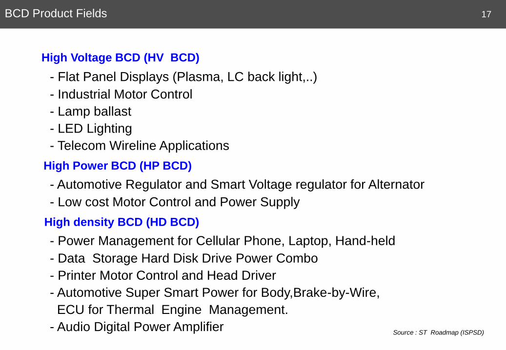
BCD Product Fields
Source : ST Roadmap (ISPSD)
High Voltage BCD (HV BCD)
- Flat Panel Displays (Plasma, LC back light,..)
- Industrial Motor Control
- Lamp ballast
- LED Lighting
- Telecom Wireline Applications
High Power BCD (HP BCD)
- Automotive Regulator and Smart Voltage regulator for Alternator
- Low cost Motor Control and Power Supply
High density BCD (HD BCD)
- Power Management for Cellular Phone, Laptop, Hand-held
- Data Storage Hard Disk Drive Power Combo
- Printer Motor Control and Head Driver
- Automotive Super Smart Power for Body,Brake-by-Wire,
ECU for Thermal Engine Management.
- Audio Digital Power Amplifier
17
0.6um BCDMOS (BCD5, ST)
• N-type epitaxial layer on P-type substrate, Junction isolation, Thick top metal
• 5V CMOS, 16V HVCMOS, 16/20/40/80V nLDMOS, 5/12V NPN, 20/40V LPNP
• Single & Double poly EEPROMSource : C.Contiero ST (ISPSD 1996)
18
0.35um BCDMOS (BD350BA, 동부하이텍)
• N-type epitaxial layer
on P-type substrate, Junction isolation, 3 metal Layers
• 3.3V, 8V CMOS, 12/30/60V HVCMOS, 20/30/50/80V nLDMOS
30V NPN, 30/60V LPNP
• Single & Double poly EEPROM
19
High Side nLDMOS (20/30V) LVCMOS (1.8V)
MVCMOS (5V)
nVDMOS (>50V) : Option
NPN (>20V)
Low Side nLDMOS (20/30V)
P-Sub
n+
PBODY
N+BL
NWELL
Deep NWell
p+STI
Channel
Stop
N-Epi
n+ n+ n+ p+ p+ p+n+ n+
DTI
n+ n+
PBODYNWELL
N+BL
N-Epi
N+SNK
NWELLNWELL PWELL
NWELL
n
+
n+ p+ n+ n+
NWELL
N+SNK
NWELL
n+ n+ p+ n+ n+ p+ n+ n+
NWELL
N+SNK
N+BL
PBODY PBODY PBODY
Channel
Stop P-Sub
D
GS D
G
D
GS D
G
D
GS S
GD
G
E B C
N-Epi
Deep NWell
Deep NWellDeep NWell
0.35um BCDMOS (Magnachip) -1
• N-type epitaxial layer
on P-type substrate, Trench isolation, 3 metals Layers
20
ED-nMOS
(Uni: 12 ~ 30V)
Bulk Zener Diode
P-Sub
n+
P+BL
p+STI
Channel
Stop
n+
HPW
n+ p+ p+n+
DTI
n+ n+
N+SNK
N+BL
N+
SNKN-
Epi
S
GD C A C
Isolated ED-nMOS
(Uni: 12/20V)
ED-pMOS
(Uni: 12 ~ 30V)
p+ p+
PWELL
n+
NWELL
S
GD S
GD
HPW
NWELL
HPW
N+B
L
GroundPoly-Si
Zener Diode
Lateral PNP
(>20V)
Substrate PNP
(>20V)
n+
N+BL
PWELL PWELL PWELL PWELL PWELL
HPW
P+BL
Channel
Stop
N-Epi
P-Sub
P+BL
PWELL
n+ n+ n+p+ p+ p+ p+ p+n+ p+ n+ p+ n+
GNDA
CC
BB EBCECB
HPW
N+B
L
N-
Epi
Deep NWellDeep NWell
Deep NWell Deep NWell
210.35um BCDMOS (Magnachip) -1
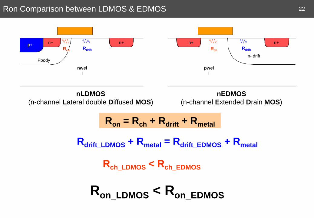
Ron Comparison between LDMOS & EDMOS
Pbody
nwel
l
nLDMOS
(n-channel Lateral double Diffused MOS)
p+n+ n+ n+ n+
nEDMOS
(n-channel Extended Drain MOS)
pwel
l
n- drift
Ron = Rch + Rdrift + Rmetal
Rdrift Rdrift
Rdrift_LDMOS + Rmetal = Rdrift_EDMOS + Rmetal
Rch Rch
Rch_LDMOS < Rch_EDMOS
Ron_LDMOS < Ron_EDMOS
22
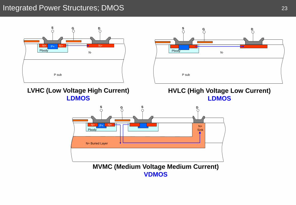
Integrated Power Structures; DMOS
N+ N+ N+
N-Pbody
P sub
S G D
P+N+ N+
LVHC (Low Voltage High Current)
LDMOSHVLC (High Voltage Low Current)
LDMOS
MVMC (Medium Voltage Medium Current)
VDMOS
P sub
PbodyN-
S G D
S G S D
Pbody
N+ Buried Layer
N+
Sink
P+
23
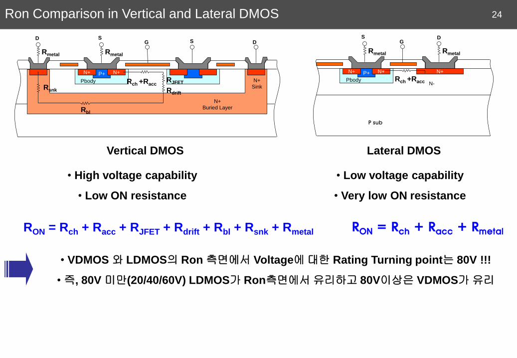
Ron Comparison in Vertical and Lateral DMOS
P+N+ N+ N+
N-Pbody
P sub
G
P+N+ N+
Vertical DMOS
SG S D
Pbody N+
Sink
D
Lateral DMOS
• High voltage capability
• Low ON resistance
N+
Buried Layer
Rsnk
Rbl
Rch +RaccRJFET
Rdrift
Rmetal Rmetal
RON = Rch + Racc + RJFET + Rdrift + Rbl + Rsnk + Rmetal
• Low voltage capability
• Very low ON resistance
Rch +Racc
S
RmetalRmetal
D
RON = Rch + Racc + Rmetal
• VDMOS 와 LDMOS의 Ron 측면에서 Voltage에대한 Rating Turning point는 80V !!!
• 즉, 80V 미만(20/40/60V) LDMOS가 Ron측면에서유리하고 80V이상은 VDMOS가유리
24
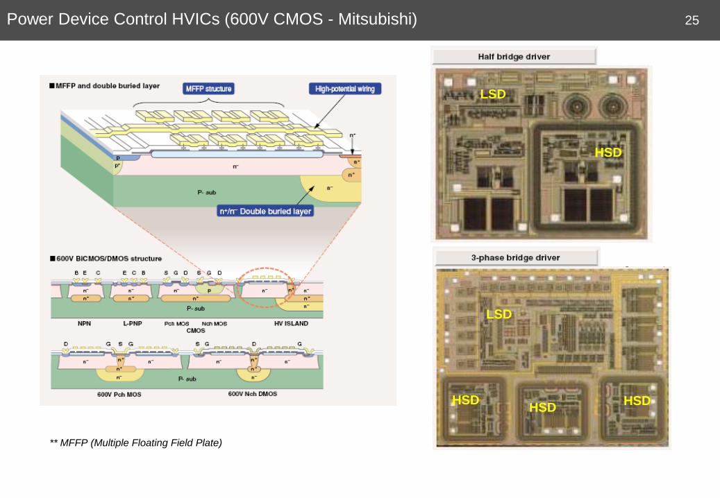
Power Device Control HVICs (600V CMOS - Mitsubishi)
LSD
HSD
LSD
HSDHSD
HSD
** MFFP (Multiple Floating Field Plate)
25
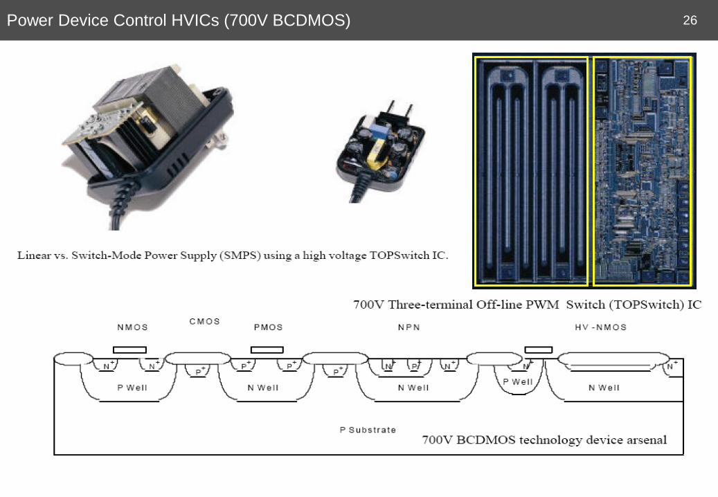
Power Device Control HVICs (700V BCDMOS) 26
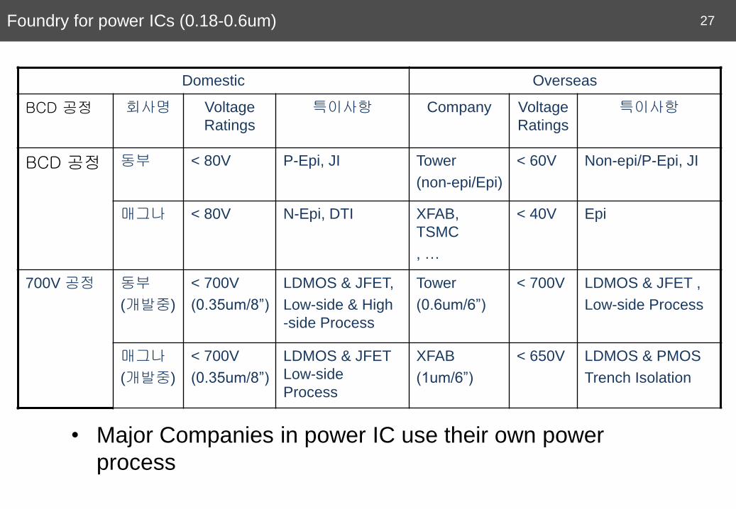
Foundry for power ICs (0.18-0.6um)
Domestic Overseas
BCD 공정 회사명 Voltage
Ratings
특이사항 Company Voltage
Ratings
특이사항
BCD 공정 동부 < 80V P-Epi, JI Tower
(non-epi/Epi)
< 60V Non-epi/P-Epi, JI
매그나 < 80V N-Epi, DTI XFAB,
TSMC
, …
< 40V Epi
700V 공정 동부
(개발중)
< 700V
(0.35um/8”)
LDMOS & JFET,
Low-side & High
-side Process
Tower
(0.6um/6”)
< 700V LDMOS & JFET ,
Low-side Process
매그나
(개발중)
< 700V
(0.35um/8”)
LDMOS & JFET
Low-side
Process
XFAB
(1um/6”)
< 650V LDMOS & PMOS
Trench Isolation
• Major Companies in power IC use their own power
process
27
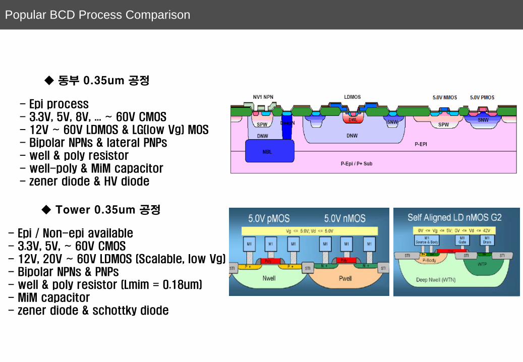
◆ 동부 0.35um 공정
- Epi process- 3.3V, 5V, 8V, ... ~ 60V CMOS- 12V ~ 60V LDMOS & LG(low Vg) MOS- Bipolar NPNs & lateral PNPs- well & poly resistor- well-poly & MiM capacitor- zener diode & HV diode
◆ Tower 0.35um 공정
- Epi / Non-epi available- 3.3V, 5V, ~ 60V CMOS- 12V, 20V ~ 60V LDMOS (Scalable, low Vg)- Bipolar NPNs & PNPs- well & poly resistor (Lmim = 0.18um)- MiM capacitor- zener diode & schottky diode
Popular BCD Process Comparison
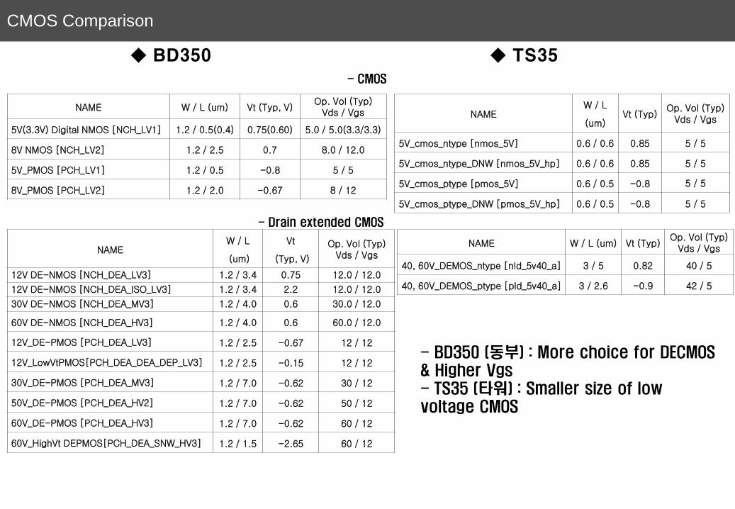
◆ BD350
- CMOS
NAME W / L (um) Vt (Typ, V)Op. Vol (Typ)
Vds / Vgs
5V(3.3V) Digital NMOS [NCH_LV1] 1.2 / 0.5(0.4) 0.75(0.60) 5.0 / 5.0(3.3/3.3)
8V NMOS [NCH_LV2] 1.2 / 2.5 0.7 8.0 / 12.0
5V_PMOS [PCH_LV1] 1.2 / 0.5 -0.8 5 / 5
8V_PMOS [PCH_LV2] 1.2 / 2.0 -0.67 8 / 12
- Drain extended CMOS
NAMEW / L
(um)
Vt
(Typ, V)
Op. Vol (Typ)Vds / Vgs
12V DE-NMOS [NCH_DEA_LV3] 1.2 / 3.4 0.75 12.0 / 12.0
12V DE-NMOS [NCH_DEA_ISO_LV3] 1.2 / 3.4 2.2 12.0 / 12.0
30V DE-NMOS [NCH_DEA_MV3] 1.2 / 4.0 0.6 30.0 / 12.0
60V DE-NMOS [NCH_DEA_HV3] 1.2 / 4.0 0.6 60.0 / 12.0
12V_DE-PMOS [PCH_DEA_LV3] 1.2 / 2.5 -0.67 12 / 12
12V_LowVtPMOS[PCH_DEA_DEA_DEP_LV3] 1.2 / 2.5 -0.15 12 / 12
30V_DE-PMOS [PCH_DEA_MV3] 1.2 / 7.0 -0.62 30 / 12
50V_DE-PMOS [PCH_DEA_HV2] 1.2 / 7.0 -0.62 50 / 12
60V_DE-PMOS [PCH_DEA_HV3] 1.2 / 7.0 -0.62 60 / 12
60V_HighVt DEPMOS[PCH_DEA_SNW_HV3] 1.2 / 1.5 -2.65 60 / 12
◆ TS35
NAMEW / L
(um)Vt (Typ)
Op. Vol (Typ)Vds / Vgs
5V_cmos_ntype [nmos_5V] 0.6 / 0.6 0.85 5 / 5
5V_cmos_ntype_DNW [nmos_5V_hp] 0.6 / 0.6 0.85 5 / 5
5V_cmos_ptype [pmos_5V] 0.6 / 0.5 -0.8 5 / 5
5V_cmos_ptype_DNW [pmos_5V_hp] 0.6 / 0.5 -0.8 5 / 5
NAME W / L (um) Vt (Typ)Op. Vol (Typ)
Vds / Vgs
40, 60V_DEMOS_ntype [nld_5v40_a] 3 / 5 0.82 40 / 5
40, 60V_DEMOS_ptype [pld_5v40_a] 3 / 2.6 -0.9 42 / 5
CMOS Comparison
- BD350 (동부) : More choice for DECMOS & Higher Vgs- TS35 (타워) : Smaller size of low voltage CMOS
NAME W / L (um) Vt (Typ)Op. Vol (Typ)
Vds / Vgs
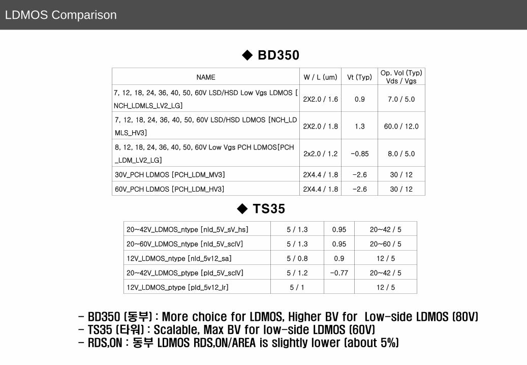
7, 12, 18, 24, 36, 40, 50, 60V LSD/HSD Low Vgs LDMOS [
NCH_LDMLS_LV2_LG]2X2.0 / 1.6 0.9 7.0 / 5.0
7, 12, 18, 24, 36, 40, 50, 60V LSD/HSD LDMOS [NCH_LD
MLS_HV3]2X2.0 / 1.8 1.3 60.0 / 12.0
8, 12, 18, 24, 36, 40, 50, 60V Low Vgs PCH LDMOS[PCH
_LDM_LV2_LG]2x2.0 / 1.2 -0.85 8.0 / 5.0
30V_PCH LDMOS [PCH_LDM_MV3] 2X4.4 / 1.8 -2.6 30 / 12
60V_PCH LDMOS [PCH_LDM_HV3] 2X4.4 / 1.8 -2.6 30 / 12
20~42V_LDMOS_ntype [nld_5V_sV_hs] 5 / 1.3 0.95 20~42 / 5
20~60V_LDMOS_ntype [nld_5V_sclV] 5 / 1.3 0.95 20~60 / 5
12V_LDMOS_ntype [nld_5v12_sa] 5 / 0.8 0.9 12 / 5
20~42V_LDMOS_ptype [pld_5V_sclV] 5 / 1.2 -0.77 20~42 / 5
12V_LDMOS_ptype [pld_5v12_lr] 5 / 1 12 / 5
- BD350 (동부) : More choice for LDMOS, Higher BV for Low-side LDMOS (80V)- TS35 (타워) : Scalable, Max BV for low-side LDMOS (60V)- RDS,ON : 동부 LDMOS RDS,ON/AREA is slightly lower (about 5%)
LDMOS Comparison
◆ BD350
◆ TS35
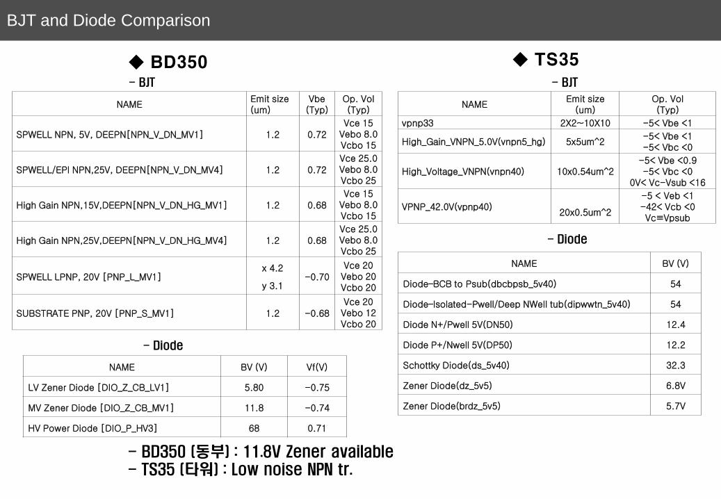
- BJT
- Diode
NAMEEmit size(um)
Vbe(Typ)
Op. Vol(Typ)
SPWELL NPN, 5V, DEEPN[NPN_V_DN_MV1] 1.2 0.72
Vce 15Vebo 8.0Vcbo 15
SPWELL/EPI NPN,25V, DEEPN[NPN_V_DN_MV4] 1.2 0.72
Vce 25.0Vebo 8.0Vcbo 25
High Gain NPN,15V,DEEPN[NPN_V_DN_HG_MV1] 1.2 0.68
Vce 15Vebo 8.0Vcbo 15
High Gain NPN,25V,DEEPN[NPN_V_DN_HG_MV4] 1.2 0.68
Vce 25.0Vebo 8.0Vcbo 25
SPWELL LPNP, 20V [PNP_L_MV1]x 4.2
y 3.1-0.70
Vce 20Vebo 20Vcbo 20
SUBSTRATE PNP, 20V [PNP_S_MV1] 1.2 -0.68
Vce 20Vebo 12Vcbo 20
NAMEEmit size
(um)Op. Vol(Typ)
vpnp33 2X2~10X10 -5< Vbe <1
High_Gain_VNPN_5.0V(vnpn5_hg) 5x5um^2-5< Vbe <1-5< Vbc <0
High_Voltage_VNPN(vnpn40) 10x0.54um^2-5< Vbe <0.9-5< Vbc <0
0V< Vc-Vsub <16
VPNP_42.0V(vpnp40)20x0.5um^2
-5 < Veb <1-42< Vcb <0Vc≡Vpsub
NAME BV (V) Vf(V)
LV Zener Diode [DIO_Z_CB_LV1] 5.80 -0.75
MV Zener Diode [DIO_Z_CB_MV1] 11.8 -0.74
HV Power Diode [DIO_P_HV3] 68 0.71
NAME BV (V)
Diode–BCB to Psub(dbcbpsb_5v40) 54
Diode–Isolated-Pwell/Deep NWell tub(dipwwtn_5v40) 54
Diode N+/Pwell 5V(DN50) 12.4
Diode P+/Nwell 5V(DP50) 12.2
Schottky Diode(ds_5v40) 32.3
Zener Diode(dz_5v5) 6.8V
Zener Diode(brdz_5v5) 5.7V
◆ BD350 ◆ TS35- BJT
- Diode
- BD350 (동부) : 11.8V Zener available- TS35 (타워) : Low noise NPN tr.
BJT and Diode Comparison
NAME W / L (um) Rs(Ohms)
POLY LSR [RES_P1L] 1.0 / 1.4 3.9
POLY MSR [RES_P1M] 1.0 / 2.1 54
POLY HSR [RES_P1H] 0.6 / 2.1 320
POLY VSR [RES_P1V] 1.0 / 2.1 2000
SNWELL Resistor [RES_SNW] 2.5 / 2.1 410
DNWELL Resistor [RES_DNW] 4.0 / 2.1 2450
NMOAT Resistor [RES_NMT] 1.2 / 1.2 68
HV NMOAT Resistor [RES_NMT_HV3] 1.2 / 1.2 52
- Resistor
NAME Rs(Ohms)
Metal 1 resistor [rm1] 80m
Metal 2 resistor [rm2] 80m
MT (20kÅA Al Thick Metal) resistor [rmt] 15m
HIPO–High Ohmic P-type Poly resistor [rphpoly3t] 1000
NMOPO–Medium Ohmic N Poly resistor [rnmpoly3t] 400
N+LOPO (Salicided Poly) resistor [rnlpoly2t] 6
N+ AA Diffusion resistor [rnplus2t, rnplus3t] 7
N-Well under STI resistor [rnwellsti2t, rnwellsti3t] 1000
P+LOPO (Salicided Poly) resistor [rplpoly2t, rplpoly3t] 5
P+ AA Diffusion resistor [rpplus2t, rpplus3t] 120
- Capacitor
NAMEW / L(um)
Op. Vol(V)
Capacitor(fF/um2)
DNWELL-POLY Capacitor [CAP_DNWP1] 10.0 / 10.0 12.0 1.15
SNWELL-POLY Capacitor [CAP_SNWP1] 10.0 / 10.0 5.0 2.70
POLY-MET1 Capacitor [CAP_P1M1] 10.0 / 10.0 66.0 0.053
MET1-MET2 Capacitor [CAP_M1M2] 10.0 / 10.0 66.0 0.050
MET2-MET3 Capacitor [CAP_M2M3] 10.0 / 10.0 66.0 0.050
MET3-MET4 Capacitor [CAP_M3M4] 10.0 / 10.0 66.0 0.050
PIP Capacitor [CAP_P1P2] 5.0 / 5.0 8 1.27
MIM Capacitor [CAP_MIM] 5.0 / 5.0 8 1
MIM Capacitor [CAP_MIM_1P8] 5.0 / 5.0 5 1.87
NAME Op. Vol (V)Capacitor(F/m2)
High-C MIM Capacitor [cmim_hc] -5~5V 1.70n
MIM Capacitor-Units [cmim_sq] -5~5V 1.0n
Ch53t 0~5V 1.852n
◆ BD350 ◆ TS35
- Capacitor
- Resistor
-TS35 (타워) : 0.18um min. length of poly resistor
Resistor and Capacitor Comparison

33
고전압 파워 IC 설계 고려 사항
34
적합한 소자의 선택 및 사용
- 소자의 내압
- Vgs 내압
Diode
- Zener
- Power Diode
DMOS & 기생 소자- Parasitic NPN, PNP
- Parasitic Diode
- Parasitic Capacitor
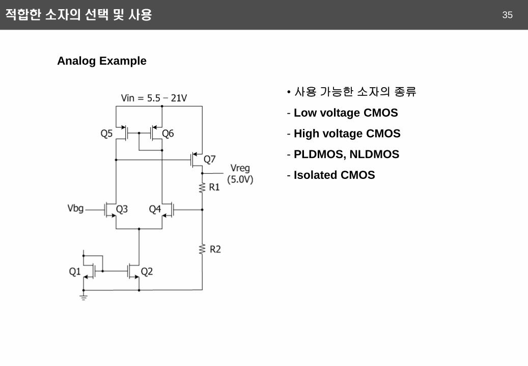
35적합한 소자의 선택 및 사용
• 사용가능한소자의종류
- Low voltage CMOS
- High voltage CMOS
- PLDMOS, NLDMOS
- Isolated CMOS
Analog Example
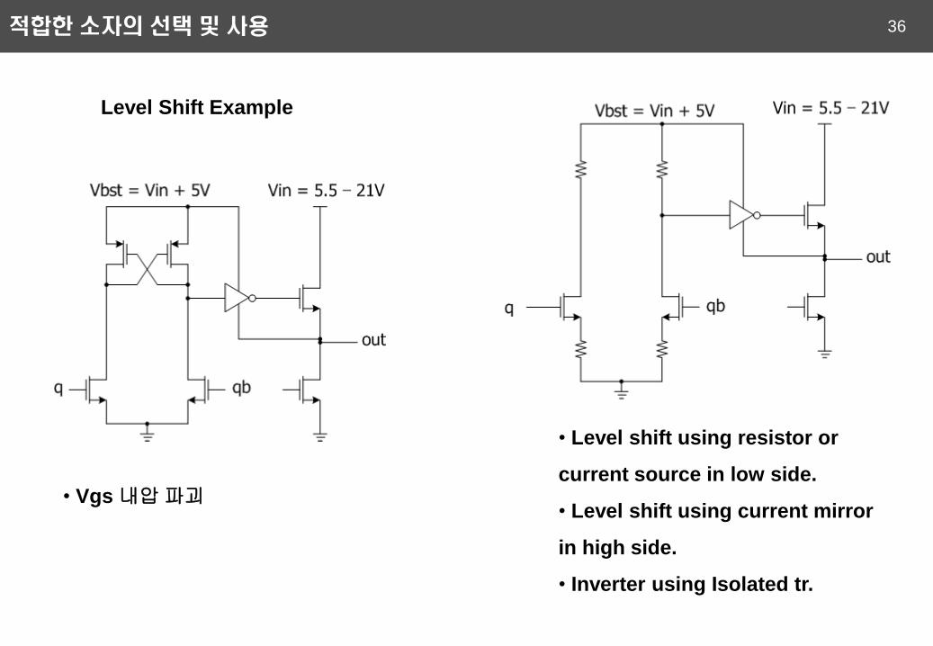
36
• Vgs 내압파괴
• Level shift using resistor or
current source in low side.
• Level shift using current mirror
in high side.
• Inverter using Isolated tr.
Level Shift Example
적합한 소자의 선택 및 사용
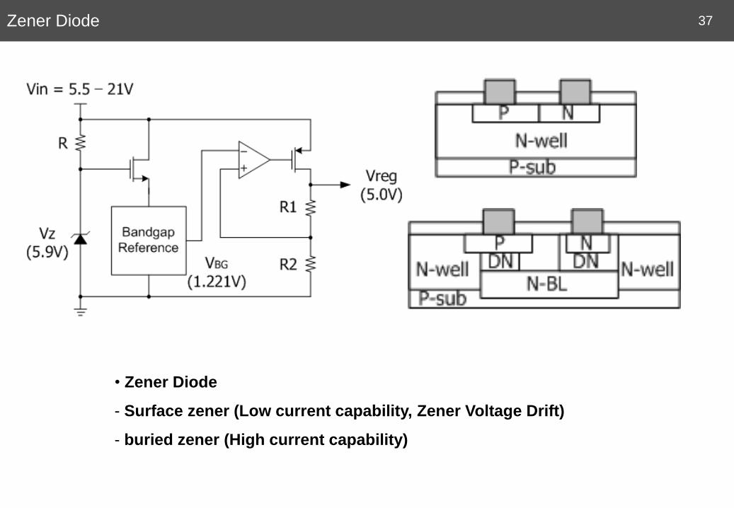
37Zener Diode
• Zener Diode
- Surface zener (Low current capability, Zener Voltage Drift)
- buried zener (High current capability)
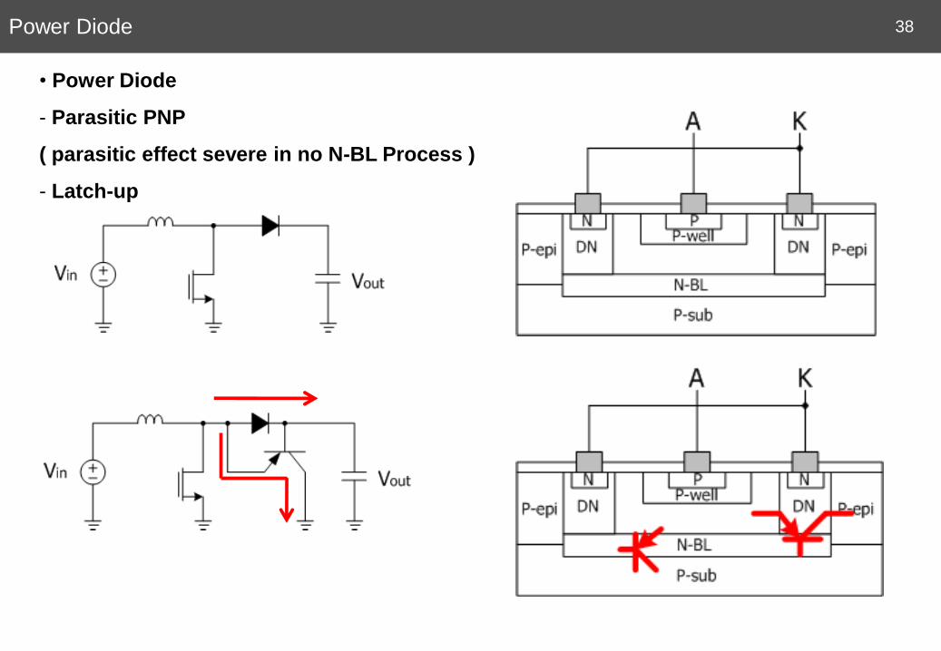
38Power Diode
• Power Diode
- Parasitic PNP
( parasitic effect severe in no N-BL Process )
- Latch-up
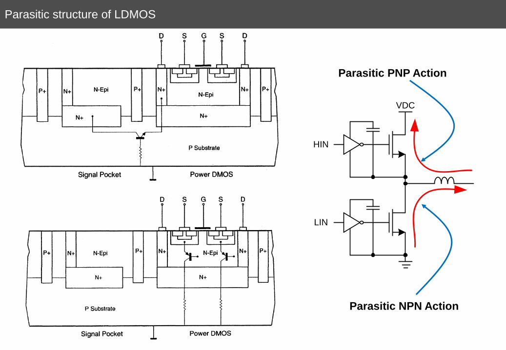
Parasitic structure of LDMOS
HIN
LIN
VDC
Parasitic PNP Action
Parasitic NPN Action
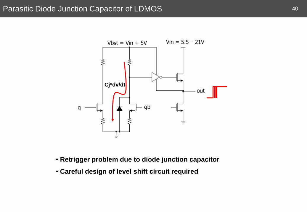
40Parasitic Diode Junction Capacitor of LDMOS
Cj*dv/dt
• Retrigger problem due to diode junction capacitor
• Careful design of level shift circuit required
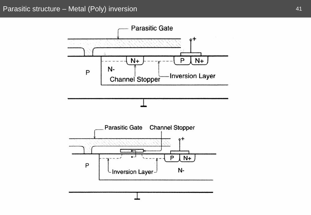
Parasitic structure – Metal (Poly) inversion 41