Embed Size (px)
Citation preview

Warm Welcome to
“Analog Circuits”

About the Lecturer
Name: Ning Beijia 宁贝佳
Office Add.: Room 104, Quarter Ⅲ, West Building
Email: [email protected]
Department: Electronic Eng. Departmentof SEE

About the Course
Objects: Undergraduate Students
Robert L. Boylestad et al.
Textbook: Electronic Devices & Circuit Theory, 9th Ed.
Class Time: 46 Hours
Final Test: Written Examination

Prerequisite
Circuit Analysisvoltage, current, resistance, capacitance, equivalent circuit
Some fundamental mathematical operations

Aim of the Course• Fundamentals of semiconductor Diode,
Bipolar Junction Transistor, Field-Effect Transistor and Operational Amplifier.
• Applications of the above mentioned analog devices.
• Analysis of power amplification circuits and feedback loops.

Structure of the Course Diode: chapter 1 & 2
BJT: chapter 3, 4 & 5
FET: chapter 6, 7 & 8
OA: chapter 10 & 11
Power Amp.: chapter 12
Feedback: chapter 13
Why Analog Circuits
Definition: An analog or analogue signal is any continuous signal for which the time varying feature of the signal is a representation of some other time varying quantity, i.e analogous to another time varying signal.

An analog signal is a measured response to changes in physical phenomena, such as sound, light, temperature, position, or pressure.
Normally, an analog signal is achieved using a transducer or sensor.

Example:
The voltage or the current is said to be an "analog" of the sound.
In sound recording, fluctuations of sound in air strike a microphone which causes corresponding fluctuations in a voltage or current in an electric circuit.

Differences to Digital Signal
Analog Signal
The values are real numbers.Small fluctuations in analog signal are meaningful.
It can appears at any time instant.
It’s easy to get affected by noise.

Digital Signal
The values are integers. Small fluctuations in digital signal are ignored.
It is meaningful only within sampling intervals.
Thus it’s robust to noise.
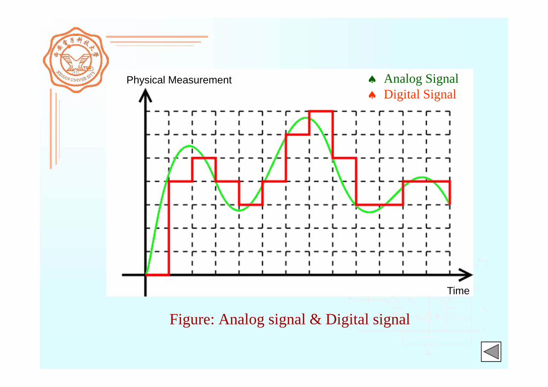
Figure: Analog signal & Digital signal
Time
Physical Measurement Analog Signal Digital Signal

Semiconductor Diodes
Semiconductor Materials
Definition:
Semiconductors are special class of elements having conductivity between that of a good conductor and that of an insulator.

Semiconductor Diodes
Semiconductors are divided into two classes:
Single-crystal: Ge (germanium) & Si (silicon)
Compound: GaAs (gallium arsenide) CdS (Cadmium sulfide)

Semiconductor Diodes
Intrinsic Materials
Definition:
Any semiconductor material that has been refined to reduce the number of impurities to a very low level, essentially as pure as can be made available through current technology.

Semiconductor Diodes
Definition:
The bonding of atoms, strengthened by the sharing of electrons, is referred to as covalence bonding.
Covalence Bonding

Semiconductor Diodes
For silicon, the four valence electrons of one atom form a bonding arrangement with four adjoining atoms, i.e. a covalence bonding.
For GaAs, sharing exists between different atoms.Five electrons are provided by arsenic atom and three by gallium atom.

Semiconductor Diodes
Figure: Covalence Bonding of the Silicon Atoms

Semiconductor Diodes
Figure: Covalence Bonding of the GaAs

Semiconductor Diodes
Covalence bond results strong bond between the valence electrons and their parent atom.
Only a few valence electrons can break covalence bond to assume free state by absorbing external energy like light or heat.
Intrinsic materials are poor conductor of electricity.

Semiconductor Diodes
Definition:
Doping is the process of intentionally introducing impurities into an intrinsic semiconductor to change its electrical properties.
Doping

Semiconductor Diodes
Definition:
A semiconductor material that has been subjected to the doping process is called an extrinsic material.
Extrinsic Materials
There two types of extrinsic materials:n-type and p-type.

Semiconductor Diodes
An n-type material is formed by doping impurity atoms that have five valence electrons, such as antimony (Sb) atoms.
n-Type Materials
The four covalence bonds still exist.
The fifth electron, loosely bound to Sb atom, is relatively free to move.

Semiconductor Diodes
Figure: Antimony impurity in n-type material

Semiconductor Diodes
The p-type material is created by doping impurity elements that have three valence electrons, such as Boron (B).
p-Type Materials
Only three covalence bonds exist.
The vacancy is called a hole, indicating the absence of a negative charge.

Semiconductor Diodes
Figure: Boron impurity in p-type material

Semiconductor Diodes
In an n-type material, the electron is called the majority carrier and the hole the minority carrier.
Majority & Minority Carrier
In a p-type material, the hole is called the majority carrier and the electron the minority carrier.The direction of conduction is conventional flow, i.e. same as hole flow and opposite to electron flow.

Semiconductor Diodes
Definition:A semiconductor diode is created by joining an n-type and a p-type material together, just the joining of one material with a majority carrier of electrons to one with a majority carrier of holes.
Semiconductor Diode

Semiconductor Diodes
Figure: Vacuum tube diode

Semiconductor Diodes
In the region of junction, electrons and holes will combine, leading to a lack of free carrier in the region near the junction.
Depletion region
The region of uncovered positive & negative ions is called the depletion region due to the “depletion” of free carriers in the region.

Semiconductor Diodes
Figure: Diode without bias

Semiconductor Diodes
The symbol for a semiconductor diode is corresponding to the p-n junction.
The bias, denoted by VD , is applied external voltage across the two terminals to extract a response.
Without bias across a diode, the net flow of charge in one direction is zero.

Semiconductor Diodes
Figure: Diode symbol & defined polarity

Semiconductor Diodes
An external potential is applied across p-njunction in the way that positive terminal is connected to the n-type material and negative to the p-type material.
Reverse-Bias Condition
The number of positive ions in the depletion region of n-type material will increase due to more free electrons drawn to the positive potential of the applied voltage.

Semiconductor Diodes
The number of negative ions in the depletion region of p-type material will increase due to more holes drawn to the negative potential of the applied voltage.
The net effect, is a widening of the depletion region.
So it’s a greater barrier for the majority carrier to overcome, leading to majority flow to zero.

Semiconductor Diodes
However, the number of minority carrier passing the depletion region will not change.
The current exists under reverse-bias condition is called the reverse saturation current, denoted by IS.
Normally, IS is only a few microamperes.

Semiconductor Diodes
Figure: Diode with reverse bias

Semiconductor Diodes
A forward-bias is established by applying the positive potential to the p-type material and the negative potential to the n-type material.
Forward-Bias Condition
The applied potential will “squeeze” the majority carriers to combine together and reduce the width of the depletion region.

Semiconductor Diodes
So a heavy majority flow across the junction occurs.
As the applied bias increases, the depletion region will decrease further, resulting in an exponential rise in current.
Typically, current ID is measured in mA and the voltage across a forward-biased diode will be less than 1 V.

Semiconductor Diodes
Figure: Diode with forward bias

Semiconductor Diodes
Figure: Silicon semiconductor diode characteristics

Semiconductor Diodes
The general characteristics of diode for the forward and reverse-bias region will conform to the following equation:
)1( / TD nVVSD eII
whereIS is the reverse saturation current
VD is the applied forward-bias voltage

Semiconductor Diodes
n is an ideality factor, assumed to be 1.
VT is called thermal voltage and is determined by
qkTVT /
T is the absolute temperature in Kelvins;
wherek is Boltzmann’s constant, ;KJoule /1038.1 23
q is magnitude of charge Coulomb19106.1

Semiconductor Diodes
When VD is too negative, the ID increases at a very rapid rate in the direction opposite to that of the positive voltage region.
Zener diode
The reverse-bias potential that results in this dramatic change in characteristics is called Zener potential, denoted by VZ.

Semiconductor Diodes
The diode employing this unique portion of the characteristics of a p-n junction is called Zener diode.
For the semiconductor diode, the “on” state will support a current in the direction of the arrow in the symbol.
The sharp change in characteristics is called Zener region.

Semiconductor Diodes
The polarity of VD and VZ are the same as would be obtained if each were a resistive element as shown in (c).
For the Zener diode, the direction of conduction is opposite to that of the arrow in the symbol.

Semiconductor Diodes
Figure: Zener region

Semiconductor Diodes
Figure: Conduction direction
(a) Zener diode; (b) semiconductor diode; (c) resistive element

Semiconductor Diodes
Summary of Chapter 1
• Intrinsic materials; Covalence bonding
• Doping; Extrinsic materials; n-Type, p-Type materials
• Semiconductor diode; Reverse bias; Forward bias; Zener diode