Embed Size (px)
Citation preview

1
The single cycle CPU
Shiftleft 2
PC
Instructionmemory
Readaddress
Instruction[31– 0]
Datamemory
Readdata
Writedata
RegistersWriteregister
Writedata
Readdata 1
Readdata 2
Readregister 1
Readregister 2
Instruction [15– 11]
Instruction [20– 16]
Instruction [25– 21]
Add
ALUresult
Zero
Instruction [5– 0]
MemtoReg
ALUOp
MemWrite
RegWrite
MemRead
Branch
JumpRegDst
ALUSrc
Instruction [31– 26]
4
Mux
Instruction [25– 0] Jump address [31– 0]
PC+4 [31– 28]
Signextend
16 32Instruction [15– 0]
1
Mux
1
0
Mux
0
1
Mux
0
1
ALUcontrol
Control
Add ALUresult
Mux
0
1 0
ALU
Shiftleft 2
26 28
Address

2
Performance of Single-Cycle Machines
• Memory Unit 2 ns• ALU and Adders 2 ns• Register file (Read or Write) 1 ns
Class Fetch Decode ALU Memory Write Back Total
R-format 2 1 2 0 1 6
LW 2 1 2 2 1 8
SW 2 1 2 2 7ns
Branch 2 1 2 5ns
Jump 2 2ns

3
עם קורה היה באורך cycleמה היה השעון שלמשתנה
•: פקודות של הבאה התערובת עם תוכנית לגבי נשווה• Rtype: 44%, LW: 24%, SW: 12% • BRANCH: 18%, JUMP: 2%
•I - בתוכנית פקודות מספר
•T - שעון מחזור אורך
•CPI - = לפקודה מחזורים 1מספר
Execution=I*T*CPI= 8*24%+7*12%+6*44%+5*18%+2*2%=6.3 ns

4
התוצאה
EXE Single cycle T single clock * I T single clock 8
EXE Variable T variable clock * I T variable clock 6.3
של פקודות. 1.27יחס נממש כאשר גרוע יותר יהיה היחסעם פעולות כמו floating pointמסובכות
. הבניה: - מבחינת מסובך משתנה בגודל שעון אינו הפתרון : של משתנה מספר לוקחת פקודה .cyclesהפתרון
5
Multicycle Approach
- ה שיטת מאחורי :Multicycleהרעיון
: השעון היחידות מספר את תקח פקודה כל בזמן חיסכוןלה.הנחוצות
: של שונים בשלבים רכיב באותו שימוש ברכיבים חיסכוןהפקודה.
6
- ה ארכיטקטורת של הבניה Multicycleשיטת
. שלב כל לשלבים הפקודה את :cycleחלק
. שלב - בכל הנדרשת העבודה כמות את אזן
רק - - יבצע שלב כל שלב בכל הנדרשת העבודה כמות את הקטן. פונקצינאלית אחת פעולה
: שעון מחזור כל בסיום
. הבאים - השלבים עבור הערכים את שמור
. נוספים - פנימיים רגיסטרים זו משימה לביצוע הוסף
7
PC
D. Memdata
D.Mem adrs
0x400000
Rs, Rt ALU inputs
ALU output(address)
Memory output
fetch Write backdecode execute
Memdata
memory
I.Mem data
PC
IR
A,B
ALUout
Mem data
MDR
fetch
Write back
decode
execute
memory
Timing of a lw instruction in a single cycle CPU
Timing of a lw instruction in a multi-cycle CPU
2ns
We want to replace a long single CK cyclewith 5 short ones:
1ns 2ns 2ns 1ns
0x400000
Instruction in IR
ALU calculates something
0 1 3 4 5=(0)2
8
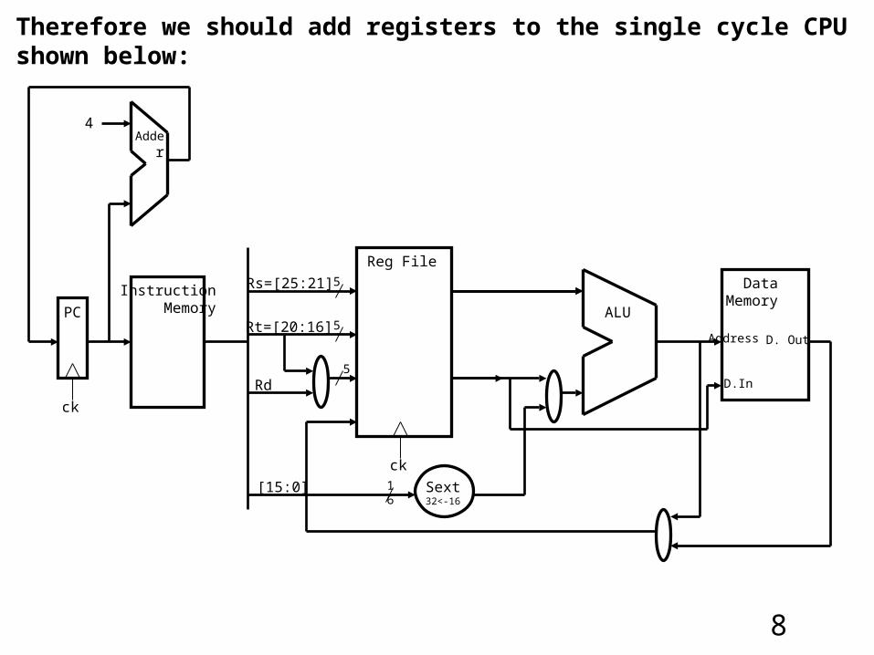
Therefore we should add registers to the single cycle CPU shown below:
5[25:21=]Rs
5[20:16=]Rt
Reg File
InstructionMemoryPC ALU
Adder4
ck
ck16[15:0]
5
Sext16>-32
DataMemory
Rd
Address
D.In
D. Out

9
Adding registers to “split” the instruction to 5 stages:
5[25:21=]Rs
5[20:16=]Rt
Reg File
InstructionMemoryPC ALU
Adder4
ck
ck16[15:0]
5
Sext16>-32
DataMemory
Rd
Address
D.In
D. Out
IR
ckck
ck
ck
ck
A
B
ALUout MDR
PCWrite
2
03
4
1
5
10
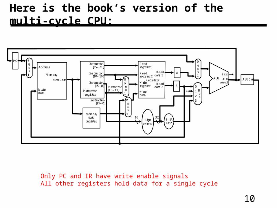
Here is the book’s version of the multi-cycle CPU:
Shiftleft 2
PC
Memory
MemData
Writedata
Mux
0
1
RegistersWriteregister
Writedata
Readdata 1
Readdata 2
Readregister 1
Readregister 2
Mux
0
1
Mux
0
1
4
Instruction[15– 0]
Signextend
3216
Instruction[25– 21]
Instruction[20– 16]
Instruction[15– 0]
Instructionregister
1 Mux
0
3
2
Mux
ALUresult
ALUZero
Memorydata
register
Instruction[15– 11]
A
B
ALUOut
0
1
Address
Only PC and IR have write enable signalsAll other registers hold data for a single cycle

11
Here is our version of A mult--cycle CPU capable of R-type & lw/sw & branch instructions
5IR[20:16]=Rt
Reg FileInstruction & dataMemory
PC
ALU
4
ck
16IR[15:0]
5
Sext16>-32
5IR[25:21]=Rs
Rd
IR
ck
IR
ck
ALUout
ck
A
ck
B
ck << 2
<<2
12
Let us explain the multi-cycle CPU
• First we’ll look at a CPU capable of performing only R-type instructions
• Then, we’ll add the lw instruction
• And the sw instruction
• Then, the beq instruction
• And finally, the j instruction

13
Let us remind ourselves how works a single cycle CPU capable of performingR-type instructions.Here you see the data-path and the timing of an R-typeinstruction.
5[25:21=]Rs
5[20:16=]Rt
5[15:11=]Rd
Reg File
InstructionMemoryPC ALU
Adder4
ck
ck
6[31:26]
6[5:0=]funct
PC 0x400000 0x400004
Rs, Rt ALU inputs new ALU inputs
ALU output
Memory output New Memory output
New ALU output
fetchWrite
backdecode execute

14
A single cycle CPU demo: R-type instruction
5[25:21=]Rs
5[20:16=]Rt
5[15:11=]Rd
Reg FileInstruction
Memory
PCALU
ck
ck
4

15
A multi cycle CPU capable of performing R-type instructions
5IR[20:16]=Rt
Reg FileInstruction & dataMemory
PC
ALU
ck5
5IR[25:21]=Rs
Rd
IR
ck
ALUout
ck
A
ck
B
ck

16
A multi cycle CPU capable of R-type & instructions
fetch
5IR[20:16]=Rt
Reg File
Instruction & dataMemory
PC
ALU
ck5
5IR[25:21]=Rs
Rd
IR
ck
ALUout
ck
A
ck
B
ck
01

17
A multi cycle CPU capable of R-type & instructions
decode
5IR[20:16]=Rt
Reg FileInstruction & dataMemory
PC
ALU
ck5
5IR[25:21]=Rs
Rd
IR
ck
ALUout
ck
A
ck
B
ck
1
2

18
A multi cycle CPU capable of R-type & instructions
execute
5IR[20:16]=Rt
Reg FileInstruction & dataMemory
PC
ck5
5IR[25:21]=Rs
Rd
IR
ck
ALUout
ck
A
ck
B
ck
ALU
2
3

19
A multi cycle CPU capable of R-type & instructions
write back
5IR[20:16]=Rt
Reg FileInstruction & dataMemory
PC
ALU
ck5
5IR[25:21]=Rs
Rd
IR
ck
ALUout
ck
A
ck
B
ck
Rd
ck3
4
20
PC
GPR input
0x400000
Rs, Rt ALU inputs
ALU output(Data = result of cala.)
Memory output = the instruction
fetch decode execute Write Back
Inst. Mem data
Mem data
IR
A,B
ALUout
fetch
Write back
decode
execute
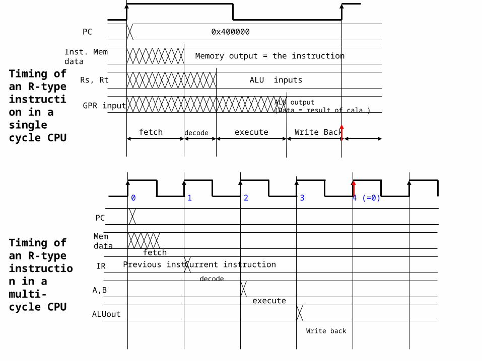
Timing of an R-type instruction in a single cycle CPU
Timing of an R-type instruction in a multi-cycle CPU
3 4 (=0)0 1 2
PC
Previous inst. Current instruction

21
Mem data
IR
A,B
ALUout
fetch
Write back
decode
execute
GPR outputs
ALUoutput
IR=M ( PC )
A= Rs, B= Rt
ALUuot= A op B
IRWrite
At the rising edge of CK:Rd=ALUoutR-Type instruction takes 4 CKs
PC
Previous inst.
Current instruction
Current instruction next inst.
IR=M(PC) A= Rs,B= Rt
ALUout = A op B Rd=ALUout
Rd = ALUout
The state diagram:

22
A multi-cycle CPU capable of R-type instructions (PC calc. )
5IR[20:16]=Rt
Reg FileInstruction & dataMemory
PC
ALU
4
ck5
5IR[25:21]=Rs
Rd
IR
ck
ALUout
ck
A
ck
B
ck
23
Mem data
IR
A,B
ALUout
fetch
Write back
decode
execute
GPR outputs
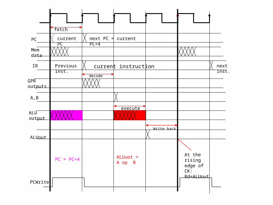
ALUoutput
ALUuot =A op B
At the rising edge of CK:Rd=ALUout
PC = PC+4
PC next PC = current PC+4current PC
next inst.Previous inst. current instruction
PCWrite

24
A multi cycle CPU capable of R-type & instructions
fetch
5IR[20:16]=Rt
Reg File
Instruction MemoryPC
ALU
ck5
5IR[25:21]=Rs
Rd
IR
ck
ALUout
ck
A
ck
B
ck
ALU
4

25
Fetch
WBR
ALU
Decode
1
6
0
7
R-type
The state diagram of a CPU capable of R-type instructions only
IR=M(PC)PC = PC+4
ALUout=A op B
A=RsB=Rt
Rd = ALUout
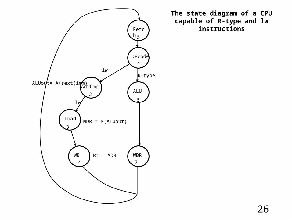
26
Fetch
WBR
Load
ALUAdrCmp
Decode
WB
1
26
0
74
3
lwR-type
lw
The state diagram of a CPU capable of R-type and lw
instructions
ALUout= A+sext(imm)
MDR = M(ALUout)
Rt = MDR
27
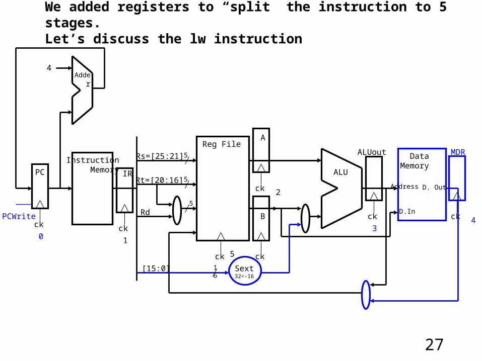
We added registers to “split” the instruction to 5 stages.Let’s discuss the lw instruction
5[25:21=]Rs
5[20:16=]Rt
Reg File
InstructionMemoryPC ALU
Adder4
ck
ck16[15:0]
5
Sext16>-32
DataMemory
Rd
Address
D.In
D. Out
IR
ckck
ck
ck
ck
A
B
ALUout MDR
PCWrite
2
03
4
1
5
28
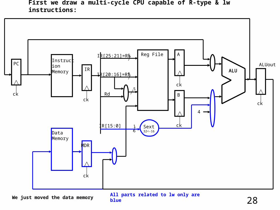
First we draw a multi-cycle CPU capable of R-type & lw instructions:
5IR[20:16]=Rt
Reg FileInstruction MemoryPC
ALU
4
ck
16IR[15:0]
5
Sext16>-32
5IR[25:21]=Rs
Rd
IR
ck
MDR
ck
ALUout
ck
A
ck
B
ck
ALUALU
We just moved the data memory All parts related to lw only are blue
Data Memory

29
A multi-cycle CPU capable of R-type & lw instructionsfetch
5IR[20:16]=Rt
Reg FileInstruction MemoryPC
ALU
4
ck
16IR[15:0]
5
Sext16>-32
5IR[25:21]=Rs
Rd
IR
ck
MDR
ck
ALUout
ck
A
ck
B
ck
ALUALU
Data Memory

30
A multi-cycle CPU capable of R-type & lw instructionsdecode
5IR[20:16]=Rt
Reg FileInstruction MemoryPC
ALU
4
ck
16IR[15:0]
5
Sext16>-32
5IR[25:21]=Rs
Rd
IR
ck
MDE
ck
ALUout
ck
A
ck
B
ck << 2Data Memory

31
A multi-cycle CPU capable of R-type & lw instructionsAdrCmp
5IR[20:16]=Rt
Reg FileInstruction MemoryPC
ALU
4
ck
16IR[15:0]
5
Sext16>-32
5IR[25:21]=Rs
Rd
IR
ck
MDR
ck
ALUout
ck
A
ck
B
ck
ALU
Data Memory

32
A multi-cycle CPU capable of R-type & lw instructionsmemory
5IR[20:16]=Rt
Reg FileInstructionMemoryPC
ALU
4
ck
16IR[15:0]
5
Sext16>-32
5IR[25:21]=Rs
Rd
Branch Address
IR
ck
MDR
ck
ALUout
ck
A
ck
B
ck << 2DataMemory

33
A multi-cycle CPU capable of R-type & lw instructionsWB
5IR[20:16]=Rt
Reg FileInstructionMemoryPC
ALU
4
ck
16IR[15:0]
5
Sext16>-32
5IR[25:21]=Rs
Rd
IR
ck
MDR
ck
ALUout
ck
A
ck
B
ck
DataMemory
ck
Rt

34
Can we unite the Instruction & Data memories? (They are not used simultaneously as in the single cycle CPU)
5IR[20:16]=Rt
Reg FileInstructionMemoryPC
ALU
4
ck
16IR[15:0]
5
Sext16>-32
5IR[25:21]=Rs
Rd
IR
ck
MDR
ck
ALUout
ck
A
ck
B
ck
DataMemory
ck

35
So here is a multi-cycle CPU capable of R-type & lw instructionsusing a single memory for instructions & data
5IR[20:16]=Rt
Reg File
PC
ALU
4
ck
16IR[15:0]
5
Sext16>-32
5IR[25:21]=Rs
Rd
IR
ck
MDR
ck
ALUout
ck
A
ck
B
ck
Instruction & dataMemory

36
PC
D. Memdata
D.Mem adrs
0x400000
Rs, Rt ALU inputs
ALU output(address)
Memory output
fetch Write backdecode execute
Memdata
memory
I.Mem data
PC
IR
A,B
ALUout
Mem data
MDR
fetch
Write back
decode
execute
memory
Timing of a lw instruction in a single cycle CPU
Timing of a lw instruction in a multi-cycle CPU
PC+4
Previous inst. current instruction
Data address
Data to Rt

37
Mem data
IR
A,B
ALUout
Mem data
MDR
fetch
Write back
decode
execute
memory
GPR outputs
ALUoutput
IR=M ( PC )PC= PC+4
A= Rs, B= Rt
ALUuot=A+sext(imm)
MDR=M(ALUout)
At the rising edge of CK:Rt=MDR
PC
Previous inst. current instruction
Data address
Data address
Data to Rt
PCWrite, IRWrite

38
Fetch
WBR
Load
ALUAdrCmp
Decode
WB
1
26
0
74
3
lwR-type
The state diagram of a CPU capable of R-type and lw
instructions
ALUout= A+sext(imm)
MDR = M(ALUout)
Rt = MDR
IR=M(PC)PC = PC+4
ALUout=A op B
A=RsB=Rt
Rd = ALUout

39
A multi-cycle CPU capable of R-type & lw & sw instructions
5IR[20:16]=Rt
Reg FileInstruction & dataMemory
PC
ALU
4
ck
16IR[15:0]
5
Sext16>-32
5IR[25:21]=Rs
Rd
Branch Address
IR
ck
MDR
ck
ALUout
ck
A
ck
B
ck << 2
lwsw

40
Fetch
WBR
Load
ALUAdrCmp
Store
Decode
WB
1
5
26
0
74
3
lw+swR-type
swlw
The state diagram of a CPU capable of R-type and lw and sw
instructions
M(ALUout)=B
IR=M(PC)PC = PC+4
ALUout=A op B
A=RsB=Rt
Rd = ALUout
ALUout= A+sext(imm)
MDR = M(ALUout)
Rt = MDR

41
A multi-cycle CPU capable of R-type & lw/sw & branch instructions
5IR[20:16]=Rt
Reg FileInstruction & dataMemory
PC
ALU
4
ck
16IR[15:0]
5
Sext16>-32
5IR[25:21]=Rs
Rd
IR
ck
IR
ck
ALUout
ck
A
ck
B
ck << 2
<<2

42
Calc PC=PC+sext(imm)<<2
Adding the instruction beq to the state diagram:
Calc Rs -Rt (just to produce the zero signal)
Fetch
WBR
Load
BranchALUAdrCmp
Store
Decode
WB
1
5
2 86
0
74
3
lw+swR-type beq
zero
swlw
not zero
43
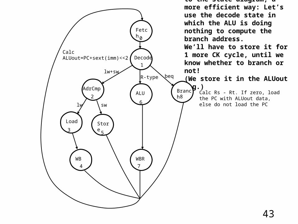
Adding the instruction beq to the state diagram, a more efficient way: Let’s use the decode state in which the ALU is doing nothing to compute the branch address.We’ll have to store it for 1 more CK cycle, until we know whether to branch or not! (We store it in the ALUout reg.)
Fetch
WBR
Load
BranchALUAdrCmp
Store
Decode
WB
1
5
2 86
0
74
3
lw+swR-type beq
swlw
Calc ALUout=PC+sext(imm)<<2
Calc Rs - Rt. If zero, load the PC with ALUout data, else do not load the PC

44
A multi-cycle CPU capable of R-type & lw/sw & branch instructions
5IR[20:16]=Rt
Reg FileInstruction & dataMemory
PC
ALU
4
ck
16IR[15:0]
5
Sext16>-32
5IR[25:21]=Rs
Rd
Branch Address
IR
ck
IR
ck
ALUout
ck
A
ck
B
ck
<<2
PC+4

45
Fetch
Jump
WBR
Load
BranchALUAdrCmp
Store
Decode
WB
1
5
2 86
9
0
74
3
lw+swR-type beq
j
swlw
Adding the instruction j to the state diagram:
PC = PC[31:28] || IR[25:0]<<2

46
A multi-cycle CPU capable of R-type & lw/sw & branch & jump instructions
5IR[20:16]=Rt
Reg FileInstruction & dataMemory
PC
ALU
4
ck
16IR[15:0]
5
Sext16>-32
5IR[25:21]=Rs
Rd
Branch Address
IR
ck
IR
ck
ALUout
ck
A
ck
B
ck
<<2
PC+4= next address
Jump addressIR[25:0]
<<2+ PC[31:28]

47
השונות הפקודות שלבי סיכום
Step nameAction for R-type
instructionsAction for memory-
reference instructionsAction for branches
Action for jumps
Instruction fetch IR = Memory[PC]PC = PC + 4
Instruction A = Reg [IR[25-21]]decode/register fetch B = Reg [IR[20-16]]
ALUOut = PC + (sign-extend (IR[15-0]) << 2)
Execution, address ALUOut = A op B ALUOut = A + sign-extend if (A ==B) then PC = PC [31-28] IIcomputation, branch/ (IR[15-0]) PC = ALUOut (IR[25-0]<<2)jump completion
Memory access or R-type Reg [IR[15-11]] = Load: MDR = Memory[ALUOut]completion ALUOut or
Store: Memory [ALUOut] = B
Memory read completion Load: Reg[IR[20-16]] = MDR5
2 8 96
1
0
7 4
3

48
MultiCycle implementation with Control
Shiftleft 2
PCMux
0
1
RegistersWriteregister
Writedata
Readdata 1
Readdata 2
Readregister 1
Readregister 2
Instruction[15– 11]
Mux
0
1
Mux
0
1
4
Instruction[15– 0]
Signextend
3216
Instruction[25– 21]
Instruction[20– 16]
Instruction[15– 0]
Instructionregister
ALUcontrol
ALUresult
ALUZero
Memorydata
register
A
B
IorD
MemRead
MemWrite
MemtoReg
PCWriteCond
PCWrite
IRWrite
ALUOp
ALUSrcB
ALUSrcA
RegDst
PCSource
RegWrite
Control
Outputs
Op[5– 0]
Instruction[31-26]
Instruction [5– 0]
Mux
0
2
Jumpaddress [31-0]Instruction [25– 0] 26 28
Shiftleft 2
PC [31-28]
1
1 Mux
0
3
2
Mux
0
1ALUOut
Memory
MemData
Writedata
Address

Final State Machine
PCWritePCSource = 10
ALUSrcA = 1ALUSrcB = 00ALUOp = 01PCWriteCond
PCSource = 01
ALUSrcA =1ALUSrcB = 00ALUOp= 10
RegDst = 1RegWrite
MemtoReg = 0
MemWriteIorD = 1
MemReadIorD = 1
ALUSrcA = 1ALUSrcB = 10ALUOp = 00
RegDst = 0RegWrite
MemtoReg =1
ALUSrcA = 0ALUSrcB = 11ALUOp = 00
MemReadALUSrcA = 0
IorD = 0IRWrite
ALUSrcB = 01ALUOp = 00
PCWritePCSource = 00
Instruction fetchInstruction decode/
register fetch
Jumpcompletion
BranchcompletionExecution
Memory addresscomputation
Memoryaccess
Memoryaccess R-type completion
Write-back step
(Op = 'LW') or (Op = 'SW') (Op = R-type)
(Op
= 'B
EQ')
(Op
= 'J
')
(Op = 'SW
')
(Op
= 'L
W')
4
01
9862
753
Start

50
Fetch
Jump
WBR
Load
BranchALUAdrCmp
Store
Decode
WB
1
5
2 86
9
0
74
3
lw+swR-type beq
j
swlw
The final state diagram:
51
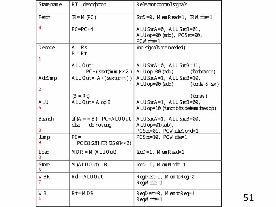
Relevant control signalsRTL descriptionState name
IorD=0, MemRead=1, IRWrite=1
ALUSrcA=0, ALUSrcB=01,ALUop=00 (add), PCSrc=00,PCWrite=1
IR= M(PC)
PC=PC+4
Fetch
0
(no signals are needed)
ALUSrcA=0, ALUSrcB=11,ALUop=00 (add) (for branch)
A = RsB = Rt
ALUOut = PC+( sext(imm)<<2 )
Decode
1
ALUSrcA=1, ALUSrcB=10,ALUop=00 (add) (for lw & sw)
(for sw)
ALUOut = A+( sext(imm) )
(B = Rt)
AdrCmp
2
ALUSrcA=1, ALUSrcB=00,ALUop=10 (funct bits determines op)
ALUOut = A op BALU6
ALUSrcA=1, ALUSrcB=00,ALUop=01(sub),PCSrc=01, PCWriteCond=1
if (A = = B) PC=ALUOutelse do nothing
Branch
8
PCSrc=10, PCWrite=1
PC= PC[31:28]||(IR[25:0]<<2)
Jump9
IorD=1, MemRead=1MDR = M(ALUOut)Load3
IorD=1, MemWrite=1M(ALUOut) = BStore5
RegDest=1, MemtoReg=0RegWrite=1
Rd = ALUOutWBR7
RegDest=0, MemtoReg=1RegWrite=1
Rt = MDRWB4

52
MultiCycle implementation with Control
Shiftleft 2
PCMux
0
1
RegistersWriteregister
Writedata
Readdata 1
Readdata 2
Readregister 1
Readregister 2
Instruction[15– 11]
Mux
0
1
Mux
0
1
4
Instruction[15– 0]
Signextend
3216
Instruction[25– 21]
Instruction[20– 16]
Instruction[15– 0]
Instructionregister
ALUcontrol
ALUresult
ALUZero
Memorydata
register
A
B
IorD
MemRead
MemWrite
MemtoReg
PCWriteCond
PCWrite
IRWrite
ALUOp
ALUSrcB
ALUSrcA
RegDst
PCSource
RegWrite
Control
Outputs
Op[5– 0]
Instruction[31-26]
Instruction [5– 0]
Mux
0
2
Jumpaddress [31-0]Instruction [25– 0] 26 28
Shiftleft 2
PC [31-28]
1
1 Mux
0
3
2
Mux
0
1ALUOut
Memory
MemData
Writedata
Address

53
• Implementation:
Finite State Machine for Control (The book’s version)
PCWrite
PCWriteCond
IorD
MemtoReg
PCSource
ALUOp
ALUSrcB
ALUSrcA
RegWrite
RegDst
NS3NS2NS1NS0
Op5
Op4
Op3
Op2
Op1
Op0
S3
S2
S1
S0
State register
IRWrite
MemRead
MemWrite
Instruction registeropcode field
Outputs
Control logic
Inputs

54
Opcode= IR[31:26]zero, neg, etc.
next state
current state
control signalsnext statecalculation
Outputs decoder
State reg
ck
The Control Finite State Machine:
For 10 states coded 0-9, we need 4 bits, i.e., [S3,S2,S1,S0]

55
The control signals decoder
We just implement the table of slide 54: Let’s look at ALUSrcA: it is “0” in states 0 and 1 and it is “1” in states 2, 6 and 8. In all other states we don’t care. let’s look at PCWrite: it is “1” in states 0 and 9. In all other states it must be “0”.And so, we’ll fill the table below and build the decoder.
S3 S2 S1 S0 ALUSrcA
state Control signals
0 10 0 0 0
01 00 0 0
0
0 0
10
1 0
X
1 X 0
0
0 00 1 0 1
PCWrite
0
1 0
11
0 0
X
1 X 0
0
All other combinations X
0 01 1
0 11 0 1
1
X
1 00 1 1
PCWriteCond
0
0
0
0
0
0
0
0
0
0
1
0
0
0
fetch
decode
AdrCmp
load
WB
store
ALU
WBR
branch
jump

56
The state machine “next state calc.” logic
R-type=000000, lw=100011, sw=101011, beq=000100, bne=000101, lui=001111, j=0000010, jal=000011, addi=001000
Fetch
0
Jump
9
WBR
7
Load
3
Branch
8ALU 6
AdrCmp 2
Store
5
Decode
1
WB
4
lw+sw
R-typebeq j
swlw
IR31 IR30 IR29 IR28 IR27 IR26
opcode
S3 S2 S1 S0
current state
S3 S2 S1 S0
next state
X 0X X X X X 0 0 0 0 0 0 1
0 0 0 1 0 1 1 00 0 00 0 0
X
X 1
0X
X X X
X X X
X
0 0 1 0
0 0 1 0
0 0 1 1
0 1 0 1
1 0X X X X X 0 0 1 0 0 1 0
R-type
lw
sw
lw+sw

57
Opcode = IR[31:26]
next state
current state
control signalsnext statecalculation
Outputs decoder
State reg
ck
The Control Finite State Machine:
Meally machine
PCWrite
PCWriteCond
zero
Mooremachine
to PC

58
Finite State Machine for ControlPCWrite
PCWriteCond
IorD
MemtoReg
PCSource
ALUOp
ALUSrcB
ALUSrcA
RegWrite
RegDst
NS3NS2NS1NS0
Op5
Op4
Op3
Op2
Op1
Op0
S3
S2
S1
S0
State register
IRWrite
MemRead
MemWrite
Instruction registeropcode field
Outputs
Control logic
Inputs
Op5
Op4
Op3
Op2
Op1
Op0
S3
S2
S1
S0
IorD
IRWrite
MemReadMemWrite
PCWritePCWriteCond
MemtoRegPCSource1
ALUOp1
ALUSrcB0ALUSrcARegWriteRegDstNS3NS2NS1NS0
ALUSrcB1ALUOp0
PCSource0
0 0 0 0 0 1 10 0 1 1 1 0 00 1 0 1 1 0 00 1 1 1 0 0 0 1 0 0 0 0 0 0 1 0 1 0 0 0 11 1 0 0 1 1 01 1 1 0 1 1 1

59
• ROM = "Read Only Memory"– values of memory locations are fixed ahead of
time• A ROM can be used to implement a truth table
– if the address is m-bits, we can address 2m entries in the ROM.
– our outputs are the bits of data that the address points to.
m is the "heigth", and n is the "width"
ROM Implementation
m n
0 0 0 0 0 1 10 0 1 1 1 0 00 1 0 1 1 0 00 1 1 1 0 0 0 1 0 0 0 0 0 0 1 0 1 0 0 0 11 1 0 0 1 1 01 1 1 0 1 1 1

60
• How many inputs are there?6 bits for opcode, 4 bits for state = 10 address
lines(i.e., 210 = 1024 different addresses)
• How many outputs are there?16 datapath-control outputs, 4 state bits = 20
outputs
• ROM is 210 x 20 = 20K bits (and a rather unusual size)
• Rather wasteful, since for lots of the entries, the outputs are the same
— i.e., opcode is often ignored
ROM Implementation

61
• Break up the table into two parts
— 4 state bits tell you the 16 outputs, 24 x 16 bits of ROM
— 10 bits tell you the 4 next state bits, 210 x 4 bits of ROM
— Total: 4.3K bits of ROM
• PLA is much smaller
— can share product terms
— only need entries that produce an active output
— can take into account don't cares
• Size is (#inputs #product-terms) + (#outputs #product-terms)
For this example = (10x17)+(20x17) = 460 PLA cells
• PLA cells usually about the size of a ROM cell (slightly bigger)
ROM vs PLA

62
Microprogramming
PCWritePCWriteCondIorD
MemtoRegPCSourceALUOpALUSrcBALUSrcARegWrite
AddrCtl
Outputs
Microcode memory
IRWrite
MemReadMemWrite
RegDst
Control unit
Input
Microprogram counter
Address select logic
Op[
5–
0]
Adder
1
Datapath
Instruction registeropcode field
BWrite

63
Microprogramming
PCWritePCWriteCondIorD
MemtoRegPCSourceALUOpALUSrcBALUSrcARegWrite
AddrCtl
Outputs
Microcode memory
IRWrite
MemReadMemWrite
RegDst
Control unit
Input
Microprogram counter
Address select logic
Op[
5–
0]
Adder
1
Datapath
Instruction registeropcode field
BWrite
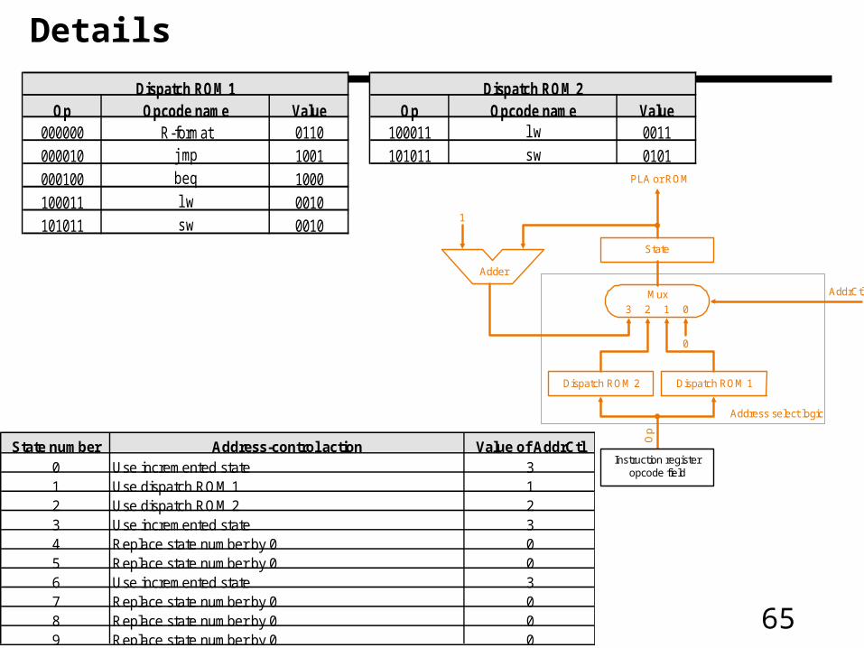
•What are the “microinstructions? ”
State
Op
Adder
1
PLA or ROM
Mux3 2 1 0
Dispatch ROM 1Dispatch ROM 2
0
AddrCtl
Address select logic
Instruction registeropcode field

64
• A specification methodology– appropriate if hundreds of opcodes, modes, cycles, etc.– signals specified symbolically using microinstructions
• Will two implementations of the same architecture have the same microcode?
• What would a microassembler do?
Microprogramming
LabelALU
control SRC1 SRC2Register control Memory
PCWrite control Sequencing
Fetch Add PC 4 Read PC ALU SeqAdd PC Extshft Read Dispatch 1
Mem1 Add A Extend Dispatch 2LW2 Read ALU Seq
Write MDR FetchSW2 Write ALU FetchRformat1 Func code A B Seq
Write ALU FetchBEQ1 Subt A B ALUOut-cond FetchJUMP1 Jump address Fetch
65
Details
Dispatch ROM 1 Dispatch ROM 2Op Opcode name Value Op Opcode name Value
000000 R-format 0110 100011 lw 0011000010 jmp 1001 101011 sw 0101000100 beq 1000100011 lw 0010101011 sw 0010
State number Address-control action Value of AddrCtl
0 Use incremented state 31 Use dispatch ROM 1 12 Use dispatch ROM 2 23 Use incremented state 34 Replace state number by 0 05 Replace state number by 0 06 Use incremented state 37 Replace state number by 0 08 Replace state number by 0 09 Replace state number by 0 0
State
Op
Adder
1
PLA or ROM
Mux3 2 1 0
Dispatch ROM 1Dispatch ROM 2
0
AddrCtl
Address select logic
Instruction registeropcode field

66
Microinstruction formatField name Value Signals active Comment
Add ALUOp = 00 Cause the ALU to add.ALU control Subt ALUOp = 01 Cause the ALU to subtract; this implements the compare for
branches.Func code ALUOp = 10 Use the instruction's function code to determine ALU control.
SRC1 PC ALUSrcA = 0 Use the PC as the first ALU input.A ALUSrcA = 1 Register A is the first ALU input.B ALUSrcB = 00 Register B is the second ALU input.
SRC2 4 ALUSrcB = 01 Use 4 as the second ALU input.Extend ALUSrcB = 10 Use output of the sign extension unit as the second ALU input.Extshft ALUSrcB = 11 Use the output of the shift-by-two unit as the second ALU input.Read Read two registers using the rs and rt fields of the IR as the register
numbers and putting the data into registers A and B.Write ALU RegWrite, Write a register using the rd field of the IR as the register number and
Register RegDst = 1, the contents of the ALUOut as the data.control MemtoReg = 0
Write MDR RegWrite, Write a register using the rt field of the IR as the register number andRegDst = 0, the contents of the MDR as the data.MemtoReg = 1
Read PC MemRead, Read memory using the PC as address; write result into IR (and lorD = 0 the MDR).
Memory Read ALU MemRead, Read memory using the ALUOut as address; write result into MDR.lorD = 1
Write ALU MemWrite, Write memory using the ALUOut as address, contents of B as thelorD = 1 data.
ALU PCSource = 00 Write the output of the ALU into the PC.PCWrite
PC write control ALUOut-cond PCSource = 01, If the Zero output of the ALU is active, write the PC with the contentsPCWriteCond of the register ALUOut.
jump address PCSource = 10, Write the PC with the jump address from the instruction.PCWrite
Seq AddrCtl = 11 Choose the next microinstruction sequentially.Sequencing Fetch AddrCtl = 00 Go to the first microinstruction to begin a new instruction.
Dispatch 1 AddrCtl = 01 Dispatch using the ROM 1.Dispatch 2 AddrCtl = 10 Dispatch using the ROM 2.

67
Microcode: Trade-offs
• Distinction between specification and implementation is sometimes blurred
• Specification Advantages:
– Easy to design and write
– Design architecture and microcode in parallel
• Implementation (off-chip ROM) Advantages
– Easy to change since values are in memory
– Can emulate other architectures
– Can make use of internal registers
• Implementation Disadvantages, SLOWER now that:
– Control is implemented on same chip as processor
– ROM is no longer faster than RAM
– No need to go back and make changes

68
Interrupt and exception
Type of event From Where ? MIPS terminology
Interrupt External I/O device request
------------------------------------------------------------------------------------
Invoke Operation system Internal Exception
From user program
-------------------------------------------------------------------------------------
Arithmetic Overflow Internal Exception
-------------------------------------------------------------------------------------
Using an undefined
Instruction Internal Exception--------------------------------------------------------------------------------------
Hardware malfunctions Either Exception or interrupt

69
Exceptions handling
Exception type Exception vector address (in hex)
Undefined instruction c0 00 00 00
Arithmetic Overflow c0 00 00 20
We have 2 ways to handle exceptions:
Cause register or Vectored interrupts
MIPS – Cause register

70
Handling exceptions

71
Handling exceptions
Shiftleft 2
Memory
MemData
Writedata
Mux
0
1
Instruction[15– 11]
Mux
0
1
4
Instruction[15– 0]
Signextend
3216
Instruction[25– 21]
Instruction[20– 16]
Instruction[15– 0]
Instructionregister
ALUcontrol
ALUresult
ALUZero
Memorydata
register
A
B
IorD
MemRead
MemWrite
MemtoReg
PCWriteCond
PCWrite
IRWrite
Control
Outputs
Op[5– 0]
Instruction[31-26]
Instruction [5– 0]
Mux
0
2
Jumpaddress [31-0]Instruction [25– 0] 26 28
Shiftleft 2
PC [31-28]
1
Address
EPC
CO 00 00 00 3
Cause
ALUOp
ALUSrcB
ALUSrcA
RegDst
PCSource
RegWrite
EPCWriteIntCauseCauseWrite
1
0
1 Mux
0
3
2
Mux
0
1
Mux
0
1
PC
Mux
0
1
RegistersWriteregister
Writedata
Readdata 1
Readdata 2
Readregister 1
Readregister 2
ALUOut

72
Shiftleft 2
PCMux
0
1
RegistersWriteregister
Writedata
Readdata 1
Readdata 2
Readregister 1
Readregister 2
Instruction[15– 11]
Mux
0
1
Mux
0
1
4
Instruction[15– 0]
Signextend
3216
Instruction[25– 21]
Instruction[20– 16]
Instruction[15– 0]
Instructionregister
ALUcontrol
ALUresult
ALUZero
Memorydata
register
A
B
IorD
MemRead
MemWrite
MemtoReg
PCWriteCond
PCWrite
IRWrite
ALUOp
ALUSrcB
ALUSrcA
RegDst
PCSource
RegWrite
Control
Outputs
Op[5– 0]
Instruction[31-26]
Instruction [5– 0]
Mux
0
2
Jumpaddress [31-0]Instruction [25– 0] 26 28
Shiftleft 2
PC [31-28]
1
1 Mux
0
3
2
Mux
0
1ALUOut
Memory
MemData
Writedata
Address

73
Fetch
Jump
WBR
Load
BranchALU
AdrCmp
Store
Decode
WB
1
5
2 86
9
0
74
3
lw+swR-type be
q
j
sw
lw
SavePC
10
IRET
1
JumpInt
11
Handling interrupts:

74
End of multi-cycle implementation