Embed Size (px)
Citation preview
LMT84Analog
I2C
36- to 50-V DC input5 V
OPA376 TPS92641
Sync-Buck Controller for LED Driver
NexFET N-Ch
MOSFETCSD18537NQ
5A
NexFET N-Ch
MOSFETCSD18563Q5
A
PWM DIM
CC2650
TPS79601Ultra-Low-Noise,
RF LDO
RC Low pass Filter
LAUNCHXL-CC2650 TIDA-01095
Temperature Sensor for LED
Ambient Light Sensor
Copyright © 2016, Texas Instruments Incorporated
33-V,100-W LED COB
Analog Dim
High side MOSFET
Low-side MOSFET
OPT3001
1TIDUBW2A–June 2016–Revised August 2016Submit Documentation Feedback
Copyright © 2016, Texas Instruments Incorporated
100-W, 0.1% Dimmable DC-DC LED Driver With Daylight Harvesting andWireless Connectivity
TI Designs100-W, 0.1% Dimmable DC-DC LED Driver With DaylightHarvesting and Wireless Connectivity
SimpleLink, PowerPAD, NexFET, e-trim, LaunchPad, BoosterPack, Code Composer Studio are trademarks of Texas Instruments.WEBENCH is a registered trademark of Texas Instruments.Cortex is a trademark of ARM Holdings.Bluetooth, Bluetooth are registered trademarks of Bluetooth SIG.Windows is a registered trademark of Microsoft Corporation.ZigBee is a registered trademark of Zigbee Alliance.All other trademarks are the property of their respective owners.
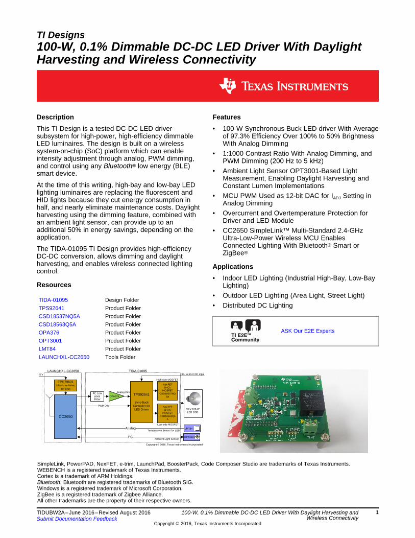
DescriptionThis TI Design is a tested DC-DC LED driversubsystem for high-power, high-efficiency dimmableLED luminaires. The design is built on a wirelesssystem-on-chip (SoC) platform which can enableintensity adjustment through analog, PWM dimming,and control using any Bluetooth® low energy (BLE)smart device.
At the time of this writing, high-bay and low-bay LEDlighting luminaires are replacing the fluorescent andHID lights because they cut energy consumption inhalf, and nearly eliminate maintenance costs. Daylightharvesting using the dimming feature, combined withan ambient light sensor, can provide up to anadditional 50% in energy savings, depending on theapplication.
The TIDA-01095 TI Design provides high-efficiencyDC-DC conversion, allows dimming and daylightharvesting, and enables wireless connected lightingcontrol.
Resources
TIDA-01095 Design FolderTPS92641 Product FolderCSD18537NQ5A Product FolderCSD18563Q5A Product FolderOPA376 Product FolderOPT3001 Product FolderLMT84 Product FolderLAUNCHXL-CC2650 Tools Folder
Features• 100-W Synchronous Buck LED driver With Average
of 97.3% Efficiency Over 100% to 50% BrightnessWith Analog Dimming
• 1:1000 Contrast Ratio With Analog Dimming, andPWM Dimming (200 Hz to 5 kHz)
• Ambient Light Sensor OPT3001-Based LightMeasurement, Enabling Daylight Harvesting andConstant Lumen Implementations
• MCU PWM Used as 12-bit DAC for IADJ Setting inAnalog Dimming
• Overcurrent and Overtemperature Protection forDriver and LED Module
• CC2650 SimpleLink™ Multi-Standard 2.4-GHzUltra-Low-Power Wireless MCU EnablesConnected Lighting With Bluetooth® Smart orZigBee®
Applications• Indoor LED Lighting (Industrial High-Bay, Low-Bay
Lighting)• Outdoor LED Lighting (Area Light, Street Light)• Distributed DC Lighting
ASK Our E2E Experts
System Overview www.ti.com
2 TIDUBW2A–June 2016–Revised August 2016Submit Documentation Feedback
Copyright © 2016, Texas Instruments Incorporated
100-W, 0.1% Dimmable DC-DC LED Driver With Daylight Harvesting andWireless Connectivity
An IMPORTANT NOTICE at the end of this TI reference design addresses authorized use, intellectual property matters and otherimportant disclaimers and information.
1 System Overview
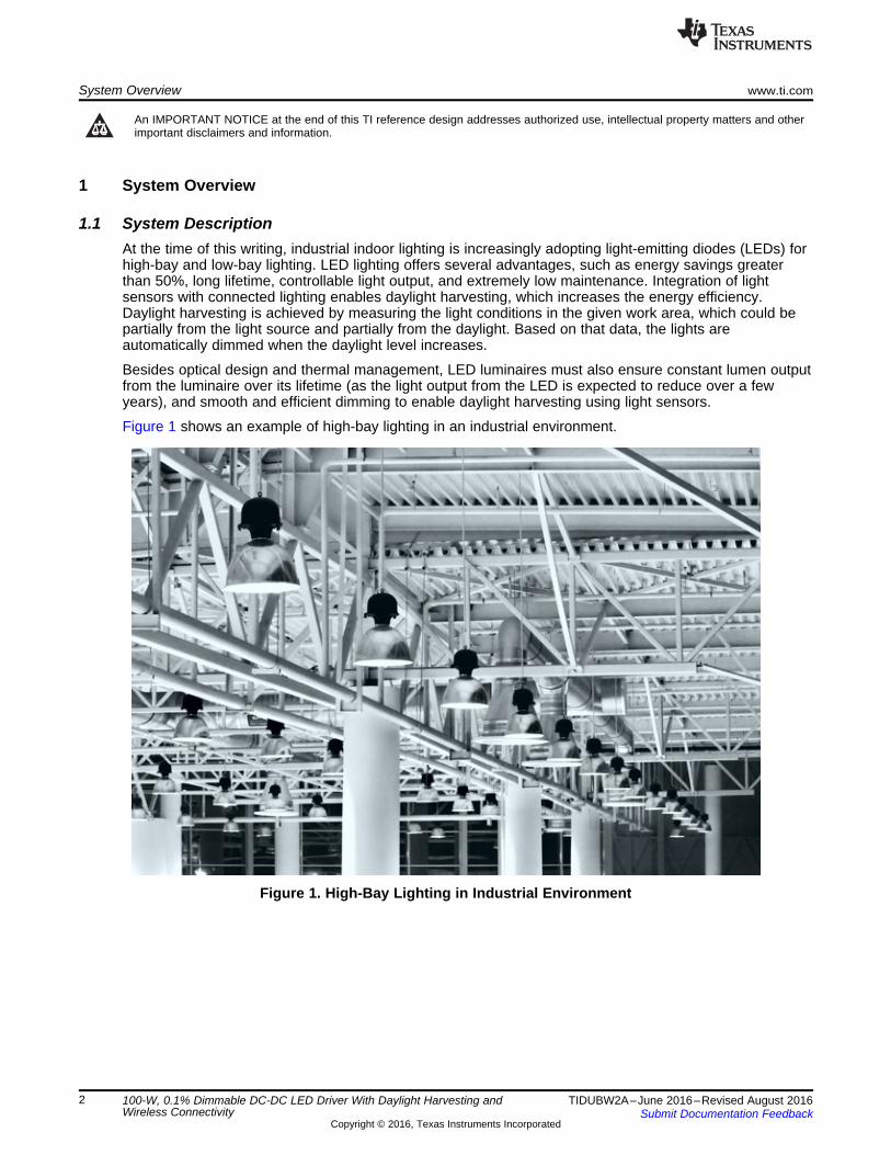
1.1 System DescriptionAt the time of this writing, industrial indoor lighting is increasingly adopting light-emitting diodes (LEDs) forhigh-bay and low-bay lighting. LED lighting offers several advantages, such as energy savings greaterthan 50%, long lifetime, controllable light output, and extremely low maintenance. Integration of lightsensors with connected lighting enables daylight harvesting, which increases the energy efficiency.Daylight harvesting is achieved by measuring the light conditions in the given work area, which could bepartially from the light source and partially from the daylight. Based on that data, the lights areautomatically dimmed when the daylight level increases.
Besides optical design and thermal management, LED luminaires must also ensure constant lumen outputfrom the luminaire over its lifetime (as the light output from the LED is expected to reduce over a fewyears), and smooth and efficient dimming to enable daylight harvesting using light sensors.
Figure 1 shows an example of high-bay lighting in an industrial environment.
Figure 1. High-Bay Lighting in Industrial Environment
www.ti.com System Overview
3TIDUBW2A–June 2016–Revised August 2016Submit Documentation Feedback
Copyright © 2016, Texas Instruments Incorporated
100-W, 0.1% Dimmable DC-DC LED Driver With Daylight Harvesting andWireless Connectivity
1.2 Key System Specifications
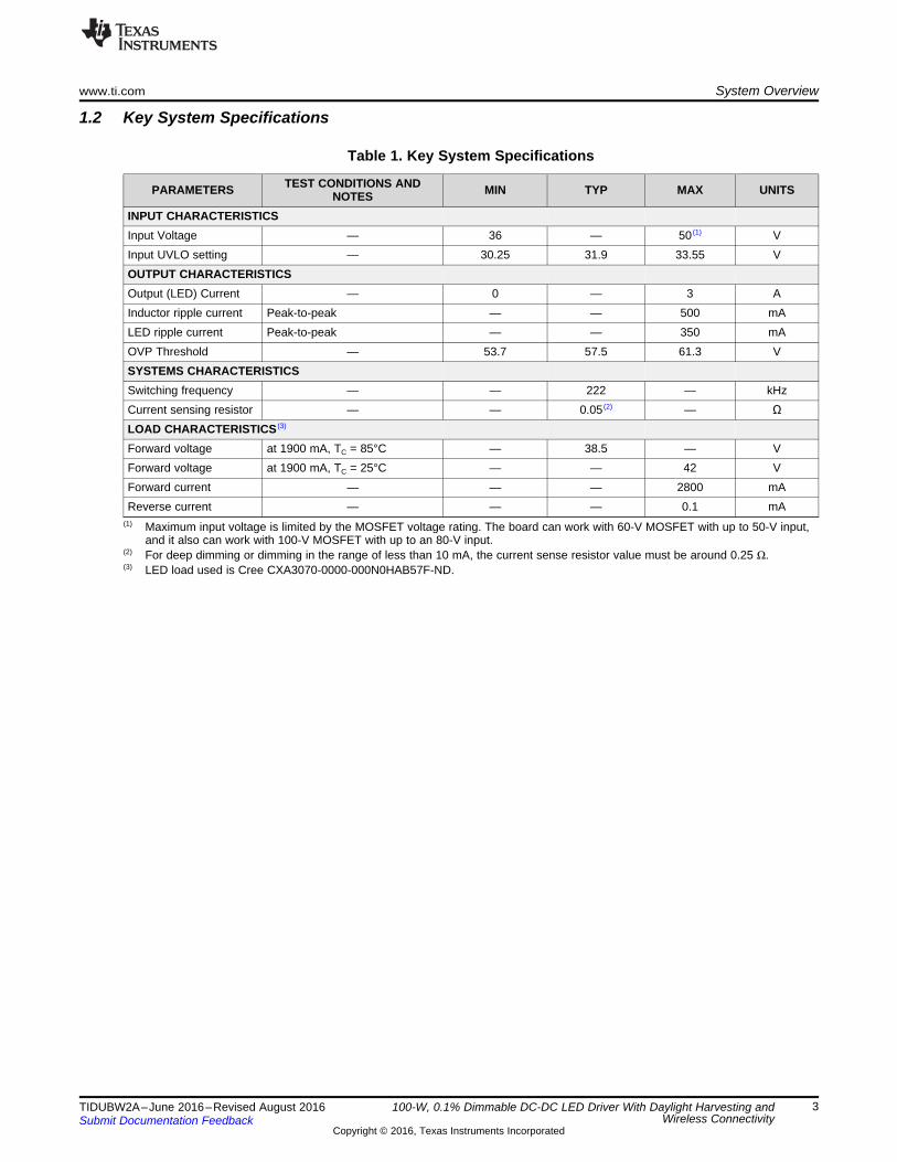
(1) Maximum input voltage is limited by the MOSFET voltage rating. The board can work with 60-V MOSFET with up to 50-V input,and it also can work with 100-V MOSFET with up to an 80-V input.
(2) For deep dimming or dimming in the range of less than 10 mA, the current sense resistor value must be around 0.25 Ω.(3) LED load used is Cree CXA3070-0000-000N0HAB57F-ND.
Table 1. Key System Specifications
PARAMETERS TEST CONDITIONS ANDNOTES MIN TYP MAX UNITS
INPUT CHARACTERISTICSInput Voltage — 36 — 50 (1) VInput UVLO setting — 30.25 31.9 33.55 VOUTPUT CHARACTERISTICSOutput (LED) Current — 0 — 3 AInductor ripple current Peak-to-peak — — 500 mALED ripple current Peak-to-peak — — 350 mAOVP Threshold — 53.7 57.5 61.3 VSYSTEMS CHARACTERISTICSSwitching frequency — — 222 — kHzCurrent sensing resistor — — 0.05 (2) — ΩLOAD CHARACTERISTICS (3)
Forward voltage at 1900 mA, TC = 85°C — 38.5 — VForward voltage at 1900 mA, TC = 25°C — — 42 VForward current — — — 2800 mAReverse current — — — 0.1 mA
LMT84Analog
I2C
36- to 50-V DC input5 V
OPA376 TPS92641
Sync-Buck Controller for LED Driver
NexFET N-Ch
MOSFET
CSD18537NQ5A
NexFET N-Ch
MOSFET
CSD18563Q5A
PWM DIM
CC2650
TPS79601Ultra-Low-Noise,
RF LDO
RC Low pass
Filter
LAUNCHXL-CC2650 TIDA-01095
Temperature Sensor for LED
Ambient Light Sensor
Copyright © 2016, Texas Instruments Incorporated
33-V,100-W LED COB
Analog Dim
High side MOSFET
Low-side MOSFET
OPT3001
System Overview www.ti.com
4 TIDUBW2A–June 2016–Revised August 2016Submit Documentation Feedback
Copyright © 2016, Texas Instruments Incorporated
100-W, 0.1% Dimmable DC-DC LED Driver With Daylight Harvesting andWireless Connectivity
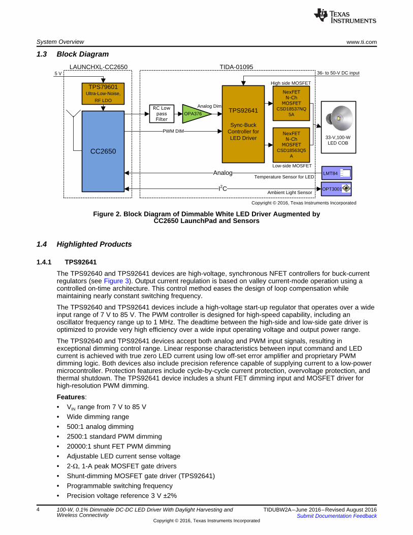
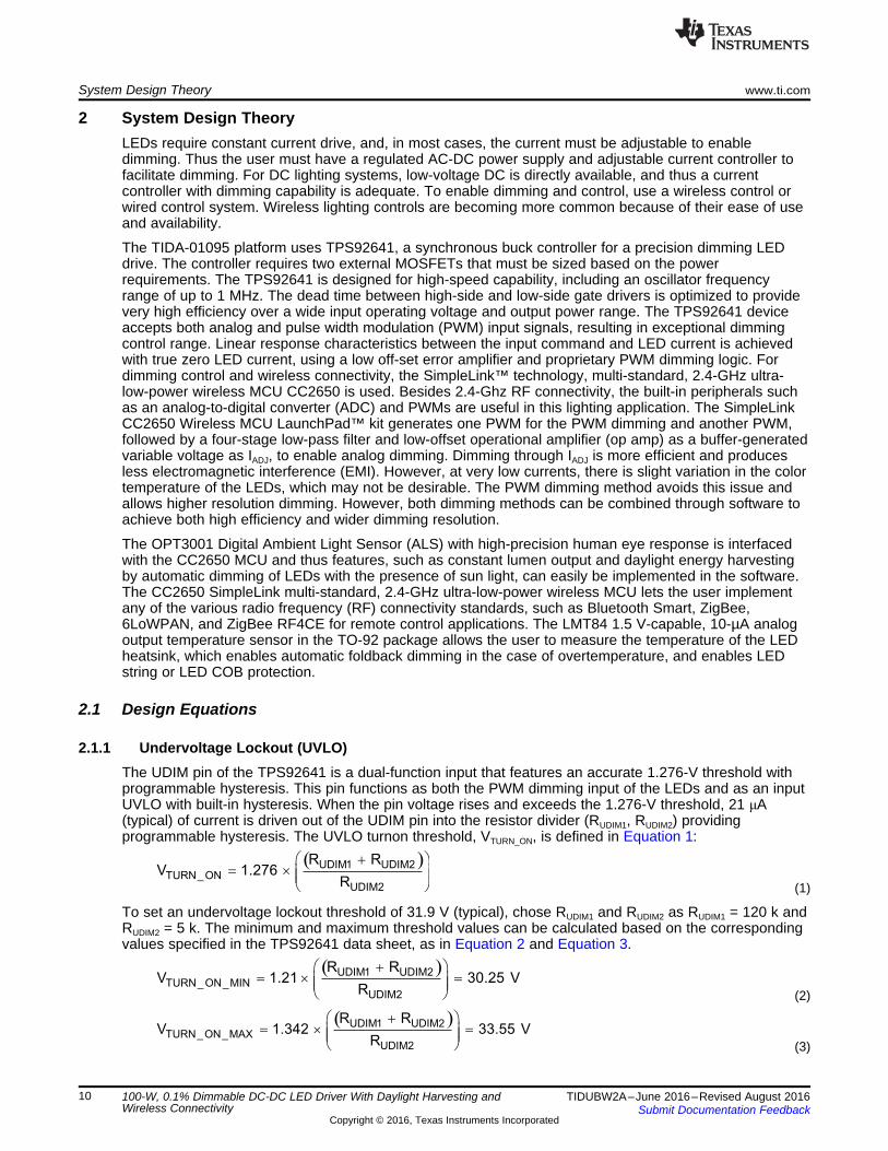
1.3 Block Diagram
Figure 2. Block Diagram of Dimmable White LED Driver Augmented byCC2650 LaunchPad and Sensors
1.4 Highlighted Products
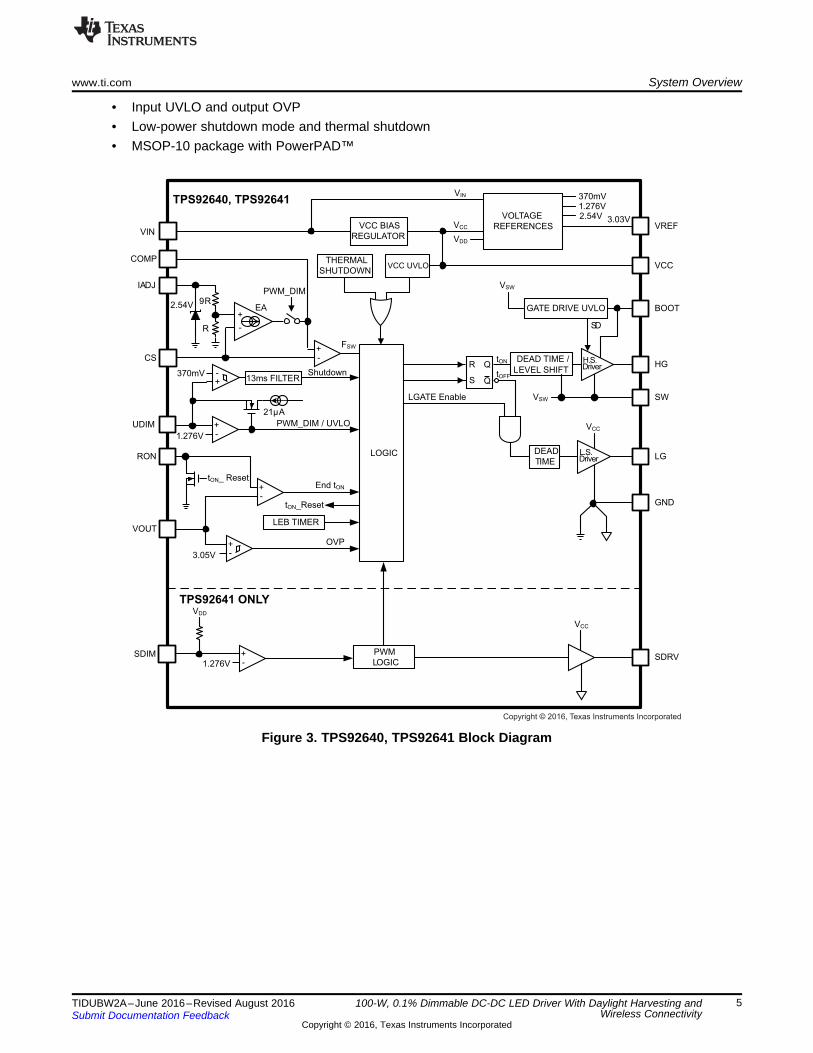
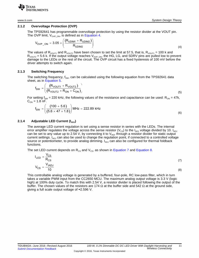
1.4.1 TPS92641The TPS92640 and TPS92641 devices are high-voltage, synchronous NFET controllers for buck-currentregulators (see Figure 3). Output current regulation is based on valley current-mode operation using acontrolled on-time architecture. This control method eases the design of loop compensation whilemaintaining nearly constant switching frequency.
The TPS92640 and TPS92641 devices include a high-voltage start-up regulator that operates over a wideinput range of 7 V to 85 V. The PWM controller is designed for high-speed capability, including anoscillator frequency range up to 1 MHz. The deadtime between the high-side and low-side gate driver isoptimized to provide very high efficiency over a wide input operating voltage and output power range.
The TPS92640 and TPS92641 devices accept both analog and PWM input signals, resulting inexceptional dimming control range. Linear response characteristics between input command and LEDcurrent is achieved with true zero LED current using low off-set error amplifier and proprietary PWMdimming logic. Both devices also include precision reference capable of supplying current to a low-powermicrocontroller. Protection features include cycle-by-cycle current protection, overvoltage protection, andthermal shutdown. The TPS92641 device includes a shunt FET dimming input and MOSFET driver forhigh-resolution PWM dimming.
Features:• VIN range from 7 V to 85 V• Wide dimming range• 500:1 analog dimming• 2500:1 standard PWM dimming• 20000:1 shunt FET PWM dimming• Adjustable LED current sense voltage• 2-Ω, 1-A peak MOSFET gate drivers• Shunt-dimming MOSFET gate driver (TPS92641)• Programmable switching frequency• Precision voltage reference 3 V ±2%
H.S.Driver
VCC
SW
BOOT
End tON
SDIM
VOUT
RON
UDIM
CS
VIN
GND
OVP
SD
HG
SDRV
VREFVOLTAGE
REFERENCES
370mV1.276V2.54V 3.03V
VCC BIAS
REGULATOR
VIN
VCC
VDD
VCC UVLOTHERMAL
SHUTDOWN
LOGIC
GATE DRIVE UVLO
VSW
Q
Q
R
S
DEAD TIME /
LEVEL SHIFT
VSW
tON
tOFF
LGATE Enable
DEAD
TIME
VCC
LG
TPS92640, TPS92641
VCC
+-3.05V
+-
LEB TIMER
tON_Reset
tON_ Reset
TPS92641 ONLY
IADJ
COMP
L.S.Driver
+-1.276V
PWM_DIM / UVLO
21µA
+-
+
-
PWM_DIM9R
R
2.54V EA
FSW
+-
VDD
1.276V
PWM
LOGIC
+-370mV
13ms FILTERShutdown
Copyright © 2016, Texas Instruments Incorporated
www.ti.com System Overview
5TIDUBW2A–June 2016–Revised August 2016Submit Documentation Feedback
Copyright © 2016, Texas Instruments Incorporated
100-W, 0.1% Dimmable DC-DC LED Driver With Daylight Harvesting andWireless Connectivity
• Input UVLO and output OVP• Low-power shutdown mode and thermal shutdown• MSOP-10 package with PowerPAD™
Figure 3. TPS92640, TPS92641 Block Diagram

System Overview www.ti.com
6 TIDUBW2A–June 2016–Revised August 2016Submit Documentation Feedback
Copyright © 2016, Texas Instruments Incorporated
100-W, 0.1% Dimmable DC-DC LED Driver With Daylight Harvesting andWireless Connectivity
1.4.2 TPS92640The TPS92640 device is a high-voltage, synchronous NFET controller for buck-current regulators from theTPS9264x device family, and can be used instead of the TPS92641 in the same design. The TPS92641device includes a shunt FET dimming input and MOSFET driver for high-frequency and high-resolutionPWM dimming, in addition to all the features provided by the TPS92640. The TPS92640 can fit in endapplications which do not exploit the shunt dimming feature of the TPS92641.
1.4.3 CSD18537NQ5AThis 10-mΩ, 60-V, SON 5×6-mm NexFET™ power MOSFET from TI is designed to minimize losses inpower conversion applications. This MOSFET is recommended to be used as the high-side MOSFET insynchronous buck converter applications.
Features:• Ultra-low Qg and Qgd
• Low thermal resistance• Avalanche rated• Pb-free terminal plating• RoHS compliant
1.4.4 CSD18563Q5AThis 5.7-mΩ, 60-V SON 5×6-mm NexFET power MOSFET is designed to pair with the CSD18537NQ5Acontrol FET, and act as the sync FET for a complete industrial buck-converter chipset solution.
Features:• Ultra-low Qg and Qgd
• Soft body diode for reduced ringing• Low thermal resistance• Avalanche rated• Logic level• Pb-free terminal plating• RoHS compliant• Halogen free• SON 5×6-mm plastic package
1.4.5 CSD18563Q5AThis 100-V, 12.6-mΩ, SON 5x6-mm NexFET power MOSFET is designed to minimize losses in powerconversion applications.
Features:• Ultra-low Qg and Qgd
• Low thermal resistance• Avalanche rated• Pb-free terminal plating• RoHS compliant• Halogen free• SON 5×6-mm plastic package
SCL
SDA
ADDR
VDD
OPT3001
INTAmbient
Light
GND
I2CInterface ADCOptical
Filter
VDD
Digital ProcessorSCL
SDA
INT or GPIO
Copyright © 2016, Texas Instruments Incorporated
www.ti.com System Overview
7TIDUBW2A–June 2016–Revised August 2016Submit Documentation Feedback
Copyright © 2016, Texas Instruments Incorporated
100-W, 0.1% Dimmable DC-DC LED Driver With Daylight Harvesting andWireless Connectivity
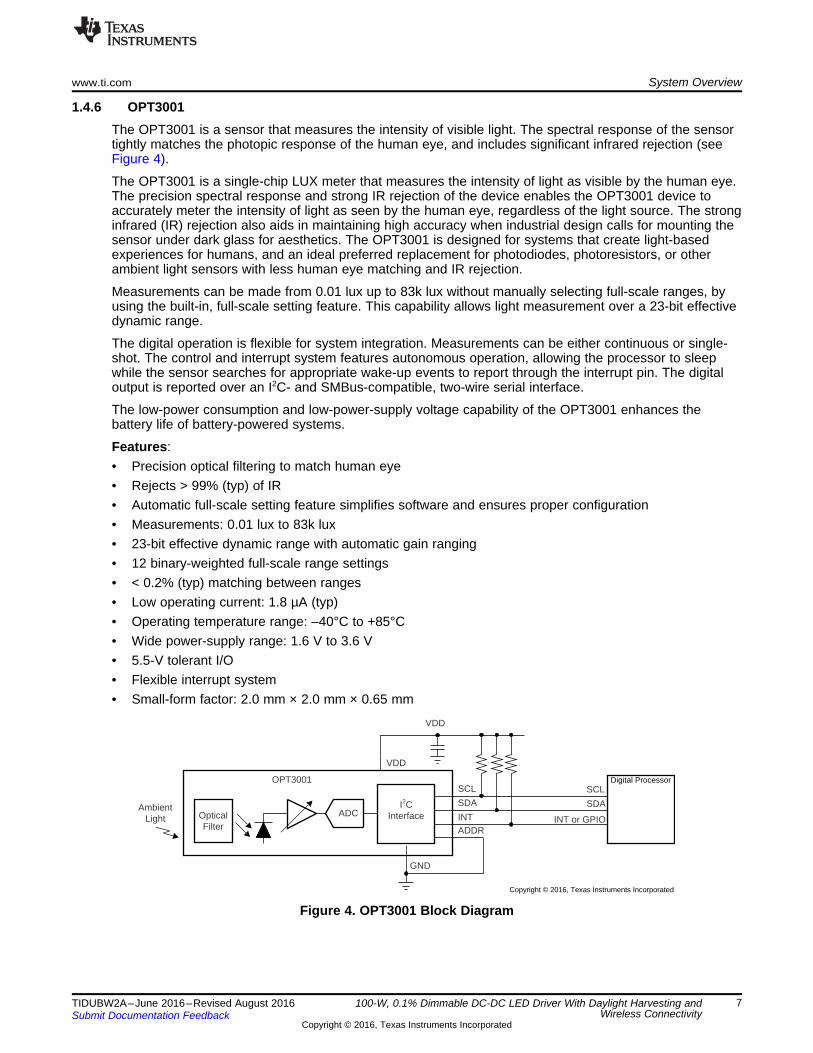
1.4.6 OPT3001The OPT3001 is a sensor that measures the intensity of visible light. The spectral response of the sensortightly matches the photopic response of the human eye, and includes significant infrared rejection (seeFigure 4).
The OPT3001 is a single-chip LUX meter that measures the intensity of light as visible by the human eye.The precision spectral response and strong IR rejection of the device enables the OPT3001 device toaccurately meter the intensity of light as seen by the human eye, regardless of the light source. The stronginfrared (IR) rejection also aids in maintaining high accuracy when industrial design calls for mounting thesensor under dark glass for aesthetics. The OPT3001 is designed for systems that create light-basedexperiences for humans, and an ideal preferred replacement for photodiodes, photoresistors, or otherambient light sensors with less human eye matching and IR rejection.
Measurements can be made from 0.01 lux up to 83k lux without manually selecting full-scale ranges, byusing the built-in, full-scale setting feature. This capability allows light measurement over a 23-bit effectivedynamic range.
The digital operation is flexible for system integration. Measurements can be either continuous or single-shot. The control and interrupt system features autonomous operation, allowing the processor to sleepwhile the sensor searches for appropriate wake-up events to report through the interrupt pin. The digitaloutput is reported over an I2C- and SMBus-compatible, two-wire serial interface.
The low-power consumption and low-power-supply voltage capability of the OPT3001 enhances thebattery life of battery-powered systems.
Features:• Precision optical filtering to match human eye• Rejects > 99% (typ) of IR• Automatic full-scale setting feature simplifies software and ensures proper configuration• Measurements: 0.01 lux to 83k lux• 23-bit effective dynamic range with automatic gain ranging• 12 binary-weighted full-scale range settings• < 0.2% (typ) matching between ranges• Low operating current: 1.8 µA (typ)• Operating temperature range: –40°C to +85°C• Wide power-supply range: 1.6 V to 3.6 V• 5.5-V tolerant I/O• Flexible interrupt system• Small-form factor: 2.0 mm × 2.0 mm × 0.65 mm
Figure 4. OPT3001 Block Diagram
System Overview www.ti.com
8 TIDUBW2A–June 2016–Revised August 2016Submit Documentation Feedback
Copyright © 2016, Texas Instruments Incorporated
100-W, 0.1% Dimmable DC-DC LED Driver With Daylight Harvesting andWireless Connectivity
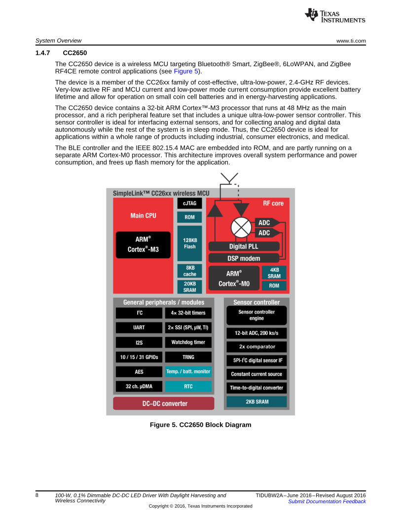
1.4.7 CC2650The CC2650 device is a wireless MCU targeting Bluetooth® Smart, ZigBee®, 6LoWPAN, and ZigBeeRF4CE remote control applications (see Figure 5).
The device is a member of the CC26xx family of cost-effective, ultra-low-power, 2.4-GHz RF devices.Very-low active RF and MCU current and low-power mode current consumption provide excellent batterylifetime and allow for operation on small coin cell batteries and in energy-harvesting applications.
The CC2650 device contains a 32-bit ARM Cortex™-M3 processor that runs at 48 MHz as the mainprocessor, and a rich peripheral feature set that includes a unique ultra-low-power sensor controller. Thissensor controller is ideal for interfacing external sensors, and for collecting analog and digital dataautonomously while the rest of the system is in sleep mode. Thus, the CC2650 device is ideal forapplications within a whole range of products including industrial, consumer electronics, and medical.
The BLE controller and the IEEE 802.15.4 MAC are embedded into ROM, and are partly running on aseparate ARM Cortex-M0 processor. This architecture improves overall system performance and powerconsumption, and frees up flash memory for the application.
Figure 5. CC2650 Block Diagram
www.ti.com System Overview
9TIDUBW2A–June 2016–Revised August 2016Submit Documentation Feedback
Copyright © 2016, Texas Instruments Incorporated
100-W, 0.1% Dimmable DC-DC LED Driver With Daylight Harvesting andWireless Connectivity
1.4.8 OPA376The OPA376 family represents a new generation of low-noise operational amplifiers with e-trim™, offeringoutstanding DC precision and AC performance. Rail-to-rail input and output, low offset (25 µV maximum),low noise (7.5 nV/√Hz), quiescent current of 950 µA (maximum), and a 5.5-MHz bandwidth make this partattractive for a variety of precision and portable applications. In addition, this device has a reasonably-wide supply range with excellent power supply rejection ratio (PSRR), which makes it desirable forapplications that run directly from batteries without regulation.
The OPA376 (single version) is available in MicroSIZE SC70-5, SOT-23-5, and SOIC-8 packages. TheOPA2376 (dual) is offered in the DSBGA-8, VSSOP-8, and SOIC-8 packages. The OPA4376 (quad) isoffered in a TSSOP-14 package. All versions are specified for operation from –40°C to +125°C.
Features:• Low noise: 7.5 nV/√Hz at 1 kHz• 0.1 Hz to 10 Hz noise: 0.8 µVPP
• Quiescent current: 760 µA (typical)• Low offset voltage: 5 µV (typ)• Gain bandwidth product: 5.5 MHz• Rail-to-rail input and output• Single-supply operation• Supply voltage: 2.2 V to 5.5 V• Space-saving packages: SC70, SOT-23, DSBGA, VSSOP, TSSOP
1.4.9 LMT84The LMT84 and LMT84-Q1 are precision CMOS integrated-circuit temperature sensors with an analogoutput voltage that is linearly and inversely proportional to temperature. The sensor features make itsuitable for many general temperature-sensing applications. The LMT84 can operate down to a 1.5-Vsupply with 5.4-µA power consumption, making it ideal for battery-powered devices.
Package options, including the through-hole TO-92 package, allows the LMT84 to be mounted onboard,off-board, to a heat sink, or on multiple locations in the same application. A class-AB output structuregives the LMT84/LMT84-Q1 strong output source and sink current capability that can directly drive up to1.1-nF capacitive loads. The LMT84 is well suited to drive an ADC sample-and-hold input with its transientload requirements. The device has accuracy specified in the operating range of −50°C to 150°C. Theaccuracy, three-lead package options, and other features also make the LMT84/LMT84-Q1 an alternativeto thermistors.
Features:• LMT84-Q1 is AEC-Q100 Grade 0 qualified and is manufactured on an automotive grade flow• Low 1.5-V operation• Very accurate: ±0.4°C typical• Wide temperature range of –50°C to 150°C• Low 5.4-µA quiescent current• Average sensor gain of –5.5 mV/°C• Output is short-circuit protected• Push-pull output with ±50-µA drive capability• Footprint compatible with the industry-standard LM20/19 and LM35 temperature sensors• Cost-effective alternative to thermistors
( )UDIM1 UDIM2TURN_ON_MAX
UDIM2
R RV 1.342 33.55 V
R
æ ö+= ´ =ç ÷ç ÷
è ø
( )UDIM1 UDIM2TURN_ON_MIN
UDIM2
R RV 1.21 30.25 V
R
æ ö+= ´ =ç ÷ç ÷
è ø
( )UDIM1 UDIM2TURN_ON
UDIM2
R RV 1.276
R
æ ö+= ´ ç ÷ç ÷
è ø
System Design Theory www.ti.com
10 TIDUBW2A–June 2016–Revised August 2016Submit Documentation Feedback
Copyright © 2016, Texas Instruments Incorporated
100-W, 0.1% Dimmable DC-DC LED Driver With Daylight Harvesting andWireless Connectivity
2 System Design TheoryLEDs require constant current drive, and, in most cases, the current must be adjustable to enabledimming. Thus the user must have a regulated AC-DC power supply and adjustable current controller tofacilitate dimming. For DC lighting systems, low-voltage DC is directly available, and thus a currentcontroller with dimming capability is adequate. To enable dimming and control, use a wireless control orwired control system. Wireless lighting controls are becoming more common because of their ease of useand availability.
The TIDA-01095 platform uses TPS92641, a synchronous buck controller for a precision dimming LEDdrive. The controller requires two external MOSFETs that must be sized based on the powerrequirements. The TPS92641 is designed for high-speed capability, including an oscillator frequencyrange of up to 1 MHz. The dead time between high-side and low-side gate drivers is optimized to providevery high efficiency over a wide input operating voltage and output power range. The TPS92641 deviceaccepts both analog and pulse width modulation (PWM) input signals, resulting in exceptional dimmingcontrol range. Linear response characteristics between the input command and LED current is achievedwith true zero LED current, using a low off-set error amplifier and proprietary PWM dimming logic. Fordimming control and wireless connectivity, the SimpleLink™ technology, multi-standard, 2.4-GHz ultra-low-power wireless MCU CC2650 is used. Besides 2.4-Ghz RF connectivity, the built-in peripherals suchas an analog-to-digital converter (ADC) and PWMs are useful in this lighting application. The SimpleLinkCC2650 Wireless MCU LaunchPad™ kit generates one PWM for the PWM dimming and another PWM,followed by a four-stage low-pass filter and low-offset operational amplifier (op amp) as a buffer-generatedvariable voltage as IADJ, to enable analog dimming. Dimming through IADJ is more efficient and producesless electromagnetic interference (EMI). However, at very low currents, there is slight variation in the colortemperature of the LEDs, which may not be desirable. The PWM dimming method avoids this issue andallows higher resolution dimming. However, both dimming methods can be combined through software toachieve both high efficiency and wider dimming resolution.
The OPT3001 Digital Ambient Light Sensor (ALS) with high-precision human eye response is interfacedwith the CC2650 MCU and thus features, such as constant lumen output and daylight energy harvestingby automatic dimming of LEDs with the presence of sun light, can easily be implemented in the software.The CC2650 SimpleLink multi-standard, 2.4-GHz ultra-low-power wireless MCU lets the user implementany of the various radio frequency (RF) connectivity standards, such as Bluetooth Smart, ZigBee,6LoWPAN, and ZigBee RF4CE for remote control applications. The LMT84 1.5 V-capable, 10-µA analogoutput temperature sensor in the TO-92 package allows the user to measure the temperature of the LEDheatsink, which enables automatic foldback dimming in the case of overtemperature, and enables LEDstring or LED COB protection.
2.1 Design Equations
2.1.1 Undervoltage Lockout (UVLO)The UDIM pin of the TPS92641 is a dual-function input that features an accurate 1.276-V threshold withprogrammable hysteresis. This pin functions as both the PWM dimming input of the LEDs and as an inputUVLO with built-in hysteresis. When the pin voltage rises and exceeds the 1.276-V threshold, 21 μA(typical) of current is driven out of the UDIM pin into the resistor divider (RUDIM1, RUDIM2) providingprogrammable hysteresis. The UVLO turnon threshold, VTURN_ON, is defined in Equation 1:
(1)
To set an undervoltage lockout threshold of 31.9 V (typical), chose RUDIM1 and RUDIM2 as RUDIM1 = 120 k andRUDIM2 = 5 k. The minimum and maximum threshold values can be calculated based on the correspondingvalues specified in the TPS92641 data sheet, as in Equation 2 and Equation 3.
(2)
(3)
IADJ
CS
VV
10=
CSLED
CS
VI
R=
( )( )SW
100 5.6f MHz 222.89 kHz
5.6 47 1.8
æ ö+= =ç ÷ç ÷´ ´è ø
( )( )
VOUT1 VOUT2
SW
VOUT2 ON ON
R Rf
R R C
æ ö+= ç ÷ç ÷´ ´è ø
( )UDIM1 UDIM2OVP _ON
UDIM2
R RV 3.05
R
æ ö+= ´ ç ÷ç ÷
è ø
www.ti.com System Design Theory
11TIDUBW2A–June 2016–Revised August 2016Submit Documentation Feedback
Copyright © 2016, Texas Instruments Incorporated
100-W, 0.1% Dimmable DC-DC LED Driver With Daylight Harvesting andWireless Connectivity
2.1.2 Overvoltage Protection (OVP)The TPS92641 has programmable overvoltage protection by using the resistor divider at the VOUT pin.The OVP limit, VOVP_ON, is defined as in Equation 4.
(4)
The values of RVOUT1 and RVOUT2 have been chosen to set the limit at 57.5, that is, RVOUT1 = 100 k andRVOUT2 = 5.6 k. If the output voltage reaches VOVP_ON, the HG, LG, and SDRV pins are pulled low to preventdamage to the LEDs or the rest of the circuit. The OVP circuit has a fixed hysteresis of 100 mV before thedriver attempts to switch again.
2.1.3 Switching FrequencyThe switching frequency, fSW, can be calculated using the following equation from the TPS92641 datasheet, as in Equation 5.
(5)
For setting fSW = 220 kHz, the following values of the resistance and capacitance can be used: RON = 47k,CON = 1.8 nF.
(6)
2.1.4 Adjustable LED Current (IADJ)The average LED current regulation is set using a sense resistor in series with the LEDs. The internalerror amplifier regulates the voltage across the sense resistor (VCS) to the IADJ voltage divided by 10. IADJcan be set to any value up to 2.54 V, by connecting it to VREF through a resistor divider for static outputcurrent settings. IADJ can also be used to change the regulation point, if connected to a controlled voltagesource or potentiometer, to provide analog dimming. IADJ can also be configured for thermal foldbackfunctions.
The set LED current depends on RCS and VCS, as shown in Equation 7 and Equation 8.
(7)
(8)
This controllable analog voltage is generated by a buffered, four-pole, RC low-pass filter, which in turntakes a variable PWM input from the CC2650 MCU. The maximum analog output voltage is 3.3 V (logichigh) at 100% duty cycle. To match this with 2.54 V, a resistor divider is placed following the output of thebuffer. The chosen values of the resistors are 174 Ω at the buffer side and 542 Ω at the ground side,giving a full scale output voltage of ≈2.596 V.
CCTRANSIENT
1
V 3.3I 3.8 mA
R 866= = =
PWM
CUTOFF
f 3.91 kHzf 391 Hz
10 10= = =
( ) ( )1
CUTOFF 1
1 1R 866
2 391 Hz 470 nF2 f C= = = W
p ´ ´p ´ ´
( ) ( )Order n 1 log 2= +
PWM PWM
Order n
V V
10 2 2=
´
PWMOrder
VRipple
10=
PWMn
VRe solutionMinimum Ripple
2 2 2= =
´
PWM
n
VRe solution
2
=
System Design Theory www.ti.com
12 TIDUBW2A–June 2016–Revised August 2016Submit Documentation Feedback
Copyright © 2016, Texas Instruments Incorporated
100-W, 0.1% Dimmable DC-DC LED Driver With Daylight Harvesting andWireless Connectivity
2.1.5 Fourth-Order Passive Low-Pass FilterTo utilize the analog dimming feature of the TPS92641, a variable analog voltage is required. This voltageis achieved by low-pass filtering the PWM generated by the CC2650 device to obtain its average value.The passive RC low-pass filter gives an analog voltage output with 12 bits of resolution, as in Equation 9.
where• Resolution is the minimum incremental change in the analog output voltage with a change in PWM
duty cycle• VPWM is the amplitude of the PWM signal• n is the resolution in bits for the analog signal (12 in this case) (9)
(10)
(11)
(12)
(13)
Therefore, the order = 13 × 0.3 = 3.9.
Round up the order to the next highest integer, if it is fractional, to achieve a higher performance than thegoal. Thus, the order = 4.
The equation that sets the cutoff frequency for a simple first-order, RC low-pass filter is given asEquation 14.
where
•• R1 and C1 = first-stage low-pass RC filter• C1 is selected arbitrarily as a standard value; choose near 1 uF as the capacitance in each subsequent
stage divided by 10 (14)
The RC filter loads the microcontroller. The load current is at a maximum when the PWM signal makes alogic level transition (such as low-to-high or high-to-low). The transient current can be estimated as shownin Equation 15.
(15)
The transient current is 3.8 mA, which is a reasonable load for the CC2650 device. To obtain a higher-order filter, additional stages of the filter can be cascaded. However, ensure that subsequent stages donot load the initial stage. A simple approach to prevent the loading is to increase the impedance of eachsubsequent stage by a factor of ten, as shown in Table 2.
www.ti.com System Design Theory
13TIDUBW2A–June 2016–Revised August 2016Submit Documentation Feedback
Copyright © 2016, Texas Instruments Incorporated
100-W, 0.1% Dimmable DC-DC LED Driver With Daylight Harvesting andWireless Connectivity
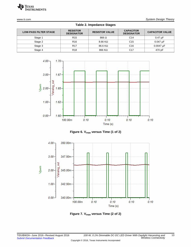
Table 2. Impedance Stages
LOW-PASS FILTER STAGE RESISTORDESIGNATOR RESISTOR VALUE CAPACITOR
DESIGNATOR CAPACITOR VALUE
Stage 1 R15 866 Ω C14 0.47 µFStage 2 R16 8.66 KΩ C15 0.047 µFStage 3 R17 86.6 KΩ C16 0.0047 µFStage 4 R18 866 KΩ C17 470 pF
Figure 6. VPWM versus Time (1 of 2)
Figure 7. VPWM versus Time (2 of 2)
( )
( )
9.35 0.81L 68.23 H
0.5 0.222
´= = m
´
OUT
IN
V 38.65D 0.81
V 48= = =
( )IN OUT
L SW
V V DL
I f
æ ö- ´= ç ÷
ç ÷D ´è ø
System Design Theory www.ti.com
14 TIDUBW2A–June 2016–Revised August 2016Submit Documentation Feedback
Copyright © 2016, Texas Instruments Incorporated
100-W, 0.1% Dimmable DC-DC LED Driver With Daylight Harvesting andWireless Connectivity
2.1.6 Control Loop Compensation (COMP)Compensating the TPS92641 is relatively simple for most applications. The only compensation required isa compensation capacitor, CCOMP across the COMP pin, and a ground to place a low-frequency dominantpole in the system. The pole must be placed low enough to ensure adequate phase margin at thecrossover frequency. For most applications, a CCOMP of 100 nF to 470 nF is adequate, and a 100-nFcapacitor has been selected for this application. Additionally, TI recommends a high-quality ceramiccapacitor with an X7R dielectric rated for 25 V.
2.1.7 Inductor SelectionBecause this is a PWM-dimming application, too much output capacitance is not recommended for fastercurrent rise and fall times, so the inductor ripple current must be close to the 500-mA peak-to-peak. Thegoverning equation which relates the inductor value (L), inductor ripple current (IL), fSW, VIN, and VOUT isshown in Equation 16.
where• In this application, VIN = 48 V• fSW = 222 kHz• VOUT = VLED + VCS = 38.5 + 0.15 = 38.65
• (16)
Thus, solve for L:
Choose the standard inductor value 68 µH, which results in an ∆IL of 501 mA.
2.1.8 LED Ripple Current SelectionLED ripple current, ΔILED, in an LED driver is the equivalent of output voltage ripple, ΔVO, in a voltageregulator. In general, the requirements for ΔILED are not as tight as the output voltage ripple. A ripple of afew mV to 4% P-P of VO is typical for ΔVO, whereas ripple currents for LED drivers range from 10% to 40%P-P of the average forward current. Allowing larger ripple current means lower inductance andcapacitance for the output filter, which in turn translates to smaller printed-circuit board (PCB) footprintsand lower bill of material (BOM) costs. For this reason, ΔILED can generally be made as large as theapplication permits. This application is designed for an LED peak-to-peak ripple current equal to 1/8th or12.5% of the maximum forward current (2800 mA = 2.8 A), ΔILED = 350 mA.
( )( )
( )
( )L LED
OUT
SW D LED
I I 0.501 0.35C F 87 nF
2 0.222 3.5691 0.352 f r I
D - D -= = m =
p ´ ´ ´p ´ ´ ´ D
( )COUT
SW OUT
1Z
2 f C=
p ´ ´
L
LED
D
COUT
II
r1
Z
DD =
æ öæ ö+ç ÷ç ÷ç ÷
è øè ø
www.ti.com System Design Theory
15TIDUBW2A–June 2016–Revised August 2016Submit Documentation Feedback
Copyright © 2016, Texas Instruments Incorporated
100-W, 0.1% Dimmable DC-DC LED Driver With Daylight Harvesting andWireless Connectivity
2.1.9 Dynamic Resistance of LEDLoad resistance is an important parameter in power supply design, particularly for the control loop. In LEDdrivers, load resistance is used to select the output capacitance required to achieve the desired LED ripplecurrent. When the load is an LED or string of LEDs, however, the load resistance is replaced with thedynamic resistance, rD, and the current sense resistor. Typical dynamic resistance at a specified forwardcurrent is provided by some manufacturers, but in most cases it must be calculated using I-V curves.
The dynamic resistance calculation for the selected LED load is done as shown in Table 3, based uponthe IV measurements.
Table 3. Forward Current and Voltage
FORWARD CURRENT (A) FORWARD VOLTAGE (V)2.748 41.802.462 40.772.169 39.751.872 38.741.578 37.741.284 36.720.991 35.680.700 34.580.409 33.29
A least square trend line can be fit in the above data to calculate the dynamic resistance. The equation ofthe trend line is V = 3.5691I + 32.038. Therefore, the dynamic resistance, rD, comes out to 4.34 Ω.
2.1.10 Output Capacitor SelectionThe LED manufacturers generally recommend values of current ripple, ΔILED, to achieve optimal opticalefficiency. The peak-to-peak current ripple values typically range from ±10% to ±40% of DC current, ILED. Acapacitor placed in parallel with the LED or array of LEDs can be used to reduce ΔILED while keeping thesame average current through both the inductor and the LED array. With this topology, the inductance canbe lowered, making the magnetics smaller and less expensive.
(17)
(18)
Rearranging Equation 17 and Equation 18 shows the relation for the required value of COUT shown inEquation 19.
(19)
Therefore, choose COUT to be 0.1 uF. The actual value of ΔILED for 0.1 uF turns out to be 334 mA.
For low dimming currents of up to 100 uA, a higher output capacitance is required to reduce the outputvoltage ripple, and thus the LED ripple current. For this purpose, a 1-uF capacitor is placed in parallel withthe calculated 0.1-uF capacitor. If low dimming currents are not required, then this component can be leftunpopulated.
T _MAX MAX LED
42I 1.5 D I 1.5 2.8 3.675 A
48
æ ö= ´ ´ = ´ ´ =ç ÷
è ø
T _MAX IN_MAXV 1.2 V 1.2 50 60 V= ´ = ´ =
( )( )
( )
( )LED
IN_MIN
IN PP SW
I D 2.8 0.81C 2.55 F
4 0.222V f-
´ -= = = m
´D ´
System Design Theory www.ti.com
16 TIDUBW2A–June 2016–Revised August 2016Submit Documentation Feedback
Copyright © 2016, Texas Instruments Incorporated
100-W, 0.1% Dimmable DC-DC LED Driver With Daylight Harvesting andWireless Connectivity
2.1.11 Minimum Input CapacitanceInput capacitance is necessary to provide instantaneous current to the discontinuous portions of the circuitduring the high side NFET on-time. The allowable input voltage ripple (ΔVIN-PP) is specified atapproximately 4 V peak-to-peak of VIN = 48 V. The minimum required capacitance (CIN_MIN) to achieve thisspecification is as in Equation 20.
(20)
TI recommends that a higher capacitance be chosen than the value calculated above, especially for PWMapplications. Thus, two capacitors, one each of 1 uF and 2.2 uF, are placed in parallel to jointly make upan equivalent capacitance of 3.2 uF.
2.1.12 MOSFET SelectionThe TPS92640 and TPS92641 devices require two external NFETs for the switching regulator. The FETsshould have a voltage rating at least 20% higher than the maximum input voltage to ensure safe operationduring the ringing of the switch node. In practice, all switching converters have some ringing at the switchnode, due to the diode parasitic capacitance and the lead inductance. The NFETs should also have acurrent rating at least 50% higher than the average transistor current. Once NFETs are chosen, the powerrating is verified by calculating the power loss.
The suggested minimum voltage rating, VT_MAX and current rating, IT_MAX are as in Equation 21 andEquation 22.
(21)
(22)
The MOSFETs chosen in this application are CSD18537NQ5A (60-V, 50-A N-Channel NexFET™ PowerMOSFET) for the high side and CSD18563Q5A (60-V, 50-A N-Channel NexFET Power MOSFET, logiclevel compatible) for the low side. These pair of MOSFETs are designed to minimize losses for powerconversion applications. Specifically, the CSD18563Q5A was designed to pair with the CSD18537NQ5Acontrol FET and act as the sync FET for a complete industrial buck converter chipset solution.
NOTE: The TIDA-01095 board is also tested with 100-V MOSFETs to enable DC-DC driveroperating voltage up to 80 V. Texas Instruments CSD19534Q5A 100 V N-Channel NexFETPower MOSFETs are used for both high-side and low-side switch.
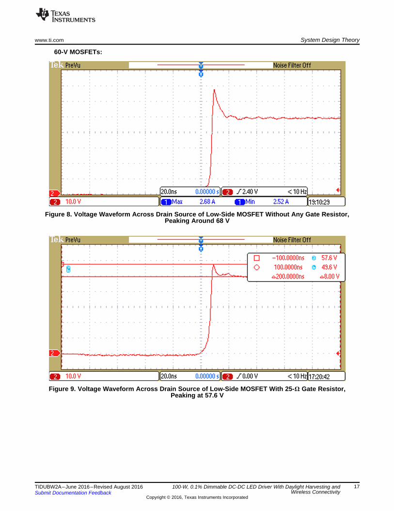
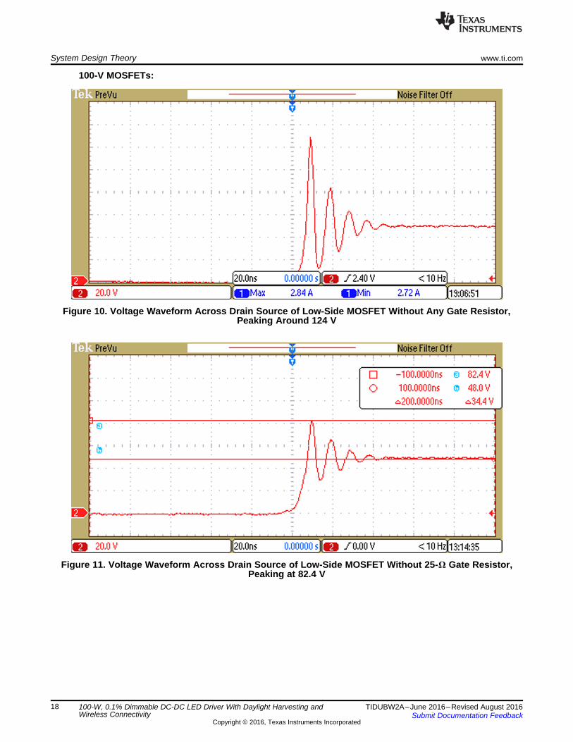
2.1.13 High-Side Gate ResistorAs the performance of power devices has improved, the control FET has the ability to switch voltages atrates greater than 10 kV/µs. However, the fast switching faces a common challenge of dealing withswitching noise. In particular, when the Control FET turns on and the Sync FET is off, the loop inductor,the loop resistor, and the output capacitor of the sync FET form a series RLC loop and resonate at aresonant frequency. This resonance results in voltage overshoot and ringing at the switch node. Using aresistor in series with the gate of the high-side FET is an effective way to reduce ringing. Similar to theboot-resistor method, this resistor slows down the turnon of the high-side FET. However, because thisresistor is in series with the gate, it is also in the discharge path, so it slows down the turnoff as well. Toreduce the ringing for this design, a 24-Ω gate resistor is used.
The following waveforms in Figure 8, Figure 9, Figure 10, and Figure 11 show the effect of the gateresistor on the switch node ringing.
www.ti.com System Design Theory
17TIDUBW2A–June 2016–Revised August 2016Submit Documentation Feedback
Copyright © 2016, Texas Instruments Incorporated
100-W, 0.1% Dimmable DC-DC LED Driver With Daylight Harvesting andWireless Connectivity
60-V MOSFETs:
Figure 8. Voltage Waveform Across Drain Source of Low-Side MOSFET Without Any Gate Resistor,Peaking Around 68 V
Figure 9. Voltage Waveform Across Drain Source of Low-Side MOSFET With 25-Ω Gate Resistor,Peaking at 57.6 V
System Design Theory www.ti.com
18 TIDUBW2A–June 2016–Revised August 2016Submit Documentation Feedback
Copyright © 2016, Texas Instruments Incorporated
100-W, 0.1% Dimmable DC-DC LED Driver With Daylight Harvesting andWireless Connectivity
100-V MOSFETs:
Figure 10. Voltage Waveform Across Drain Source of Low-Side MOSFET Without Any Gate Resistor,Peaking Around 124 V
Figure 11. Voltage Waveform Across Drain Source of Low-Side MOSFET Without 25-Ω Gate Resistor,Peaking at 82.4 V
DIM_LED DIM LEDI D I= ´
www.ti.com System Design Theory
19TIDUBW2A–June 2016–Revised August 2016Submit Documentation Feedback
Copyright © 2016, Texas Instruments Incorporated
100-W, 0.1% Dimmable DC-DC LED Driver With Daylight Harvesting andWireless Connectivity
2.2 Dimming Techniques
2.2.1 Analog Dimming Using IADJ
The LED current can be set and controlled dynamically by using the IADJ pin of the TPS92641 device. Inthis application, the VIADJ voltage is obtained from a fourth-order passive LPF followed by an OPA376operational amplifier used as a voltage follower. This low-pass filter converts the digital PWM waveform(logic high – 3.3 V and logic low – 0 V) from the CC2650 to an analog voltage equal to the average valueof the PWM waveform. The output of the op-amp feeds a resistor divider to scale the maximum possibleinput voltage from 3.3 V to 1.57 V as desired, and to not let the LED current exceed 3 A, the set maximumvalue. Refer to Section 4 for the set of measurements taken using this feature.
The fourth-order low pass filter is designed for PWM frequencies of 3.91 kHz and above. The operatingfrequency of the CC2650 MCU is fMCU = 48 MHz. This corresponds to the cycle time of:TMCU = 125 / 6 = 20.83 ns. The desired PWM frequency is generated by counting these cycles.To generate a PWM frequency of fPWM, the MCU cycles must be counted until TPWM / TMCU, whereTPWM = 1 / fPWM.
The following list provides more details:• For the counts: NPWM = TPWM / TMCU = fMCU / fPWM = 48,000,000 / fPWM.• For any chosen fPWM, the minimum possible duty cycle (resolution of the PWM) can be obtained by
keeping the corresponding I/O pin high for the duration of only 1 MCU cycle, that is, 1 count.• The PWM resolution = 1 / NPWM × 100%.• For fPWM = 4 kHz, the PWM resolution is 0.0083%. Thus, one count results in an incremental output
voltage of 0.0083% of 3.3 V = 0.275 mV at the output of the buffer.
2.2.2 Digital PWM Dimming Using UDIMThe UDIM pin can be driven with a PWM signal, which controls the synchronous NFET operation. Thebrightness of the LEDs can be varied by modulating the duty cycle (DDIM) of this signal using a Schottkydiode with an anode connected to the UDIM pin. The resulting dimmed LED current (IDIM_LED) is given as inEquation 23.
(23)
This PWM is generated using the CC2650 MCU, and the operation of this feature has been tested forPWM frequencies of 1 kHz and 5 kHz. Refer to Section 4 for the set of measurements taken using thisfeature.
VIADJ (V)
I OU
T (
mA
)
0.069 0.07 0.071 0.072 0.073 0.074 0.075 0.076 0.0770
0.2
0.4
0.6
0.8
1
1.2
D001
System Design Theory www.ti.com
20 TIDUBW2A–June 2016–Revised August 2016Submit Documentation Feedback
Copyright © 2016, Texas Instruments Incorporated
100-W, 0.1% Dimmable DC-DC LED Driver With Daylight Harvesting andWireless Connectivity
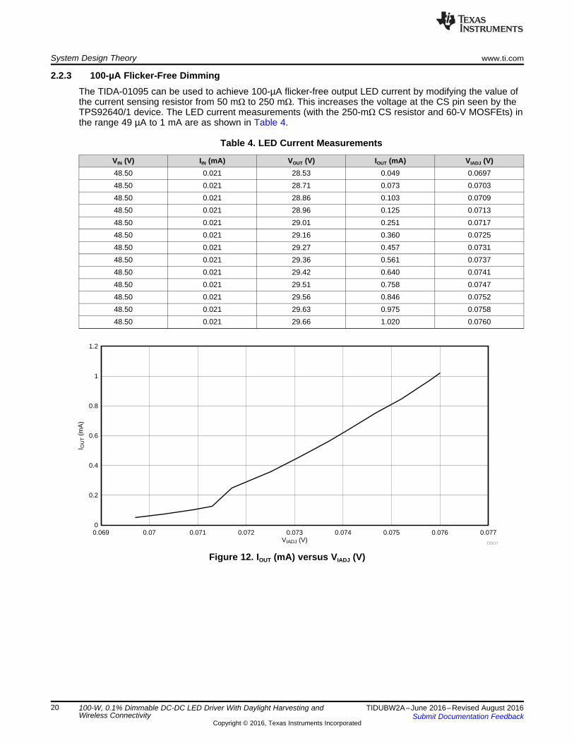
2.2.3 100-µA Flicker-Free DimmingThe TIDA-01095 can be used to achieve 100-µA flicker-free output LED current by modifying the value ofthe current sensing resistor from 50 mΩ to 250 mΩ. This increases the voltage at the CS pin seen by theTPS92640/1 device. The LED current measurements (with the 250-mΩ CS resistor and 60-V MOSFEts) inthe range 49 µA to 1 mA are as shown in Table 4.
Table 4. LED Current Measurements
VIN (V) IIN (mA) VOUT (V) IOUT (mA) VIADJ (V)48.50 0.021 28.53 0.049 0.069748.50 0.021 28.71 0.073 0.070348.50 0.021 28.86 0.103 0.070948.50 0.021 28.96 0.125 0.071348.50 0.021 29.01 0.251 0.071748.50 0.021 29.16 0.360 0.072548.50 0.021 29.27 0.457 0.073148.50 0.021 29.36 0.561 0.073748.50 0.021 29.42 0.640 0.074148.50 0.021 29.51 0.758 0.074748.50 0.021 29.56 0.846 0.075248.50 0.021 29.63 0.975 0.075848.50 0.021 29.66 1.020 0.0760
Figure 12. IOUT (mA) versus VIADJ (V)
CC2650 /DXQFK3DG
OPT3001EVM
LMT84
DC Input Voltage
PWM DIM
(PWM Input) forAnalog DIM
Constant currentLED Output
CC2541 BLE DeviceMonitor (Connected to USB Port)
Control Option 1
Control Option 2
LED mounted on heat sink to which LMT84 is affixed
USB Power andDebug to PC
Copyright © 2016, Texas Instruments Incorporated
TIDA-01095
www.ti.com Getting Started Hardware and Software
21TIDUBW2A–June 2016–Revised August 2016Submit Documentation Feedback
Copyright © 2016, Texas Instruments Incorporated
100-W, 0.1% Dimmable DC-DC LED Driver With Daylight Harvesting andWireless Connectivity
3 Getting Started Hardware and Software
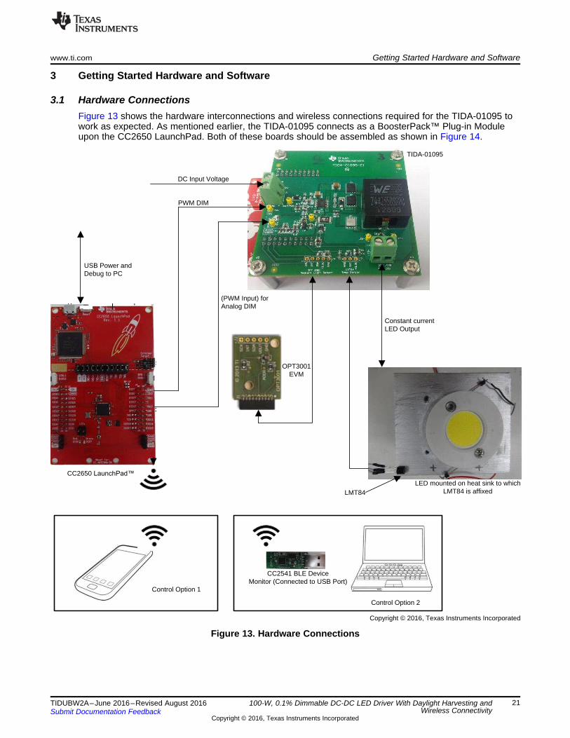
3.1 Hardware ConnectionsFigure 13 shows the hardware interconnections and wireless connections required for the TIDA-01095 towork as expected. As mentioned earlier, the TIDA-01095 connects as a BoosterPack™ Plug-in Moduleupon the CC2650 LaunchPad. Both of these boards should be assembled as shown in Figure 14.
Figure 13. Hardware Connections
Getting Started Hardware and Software www.ti.com
22 TIDUBW2A–June 2016–Revised August 2016Submit Documentation Feedback
Copyright © 2016, Texas Instruments Incorporated
100-W, 0.1% Dimmable DC-DC LED Driver With Daylight Harvesting andWireless Connectivity
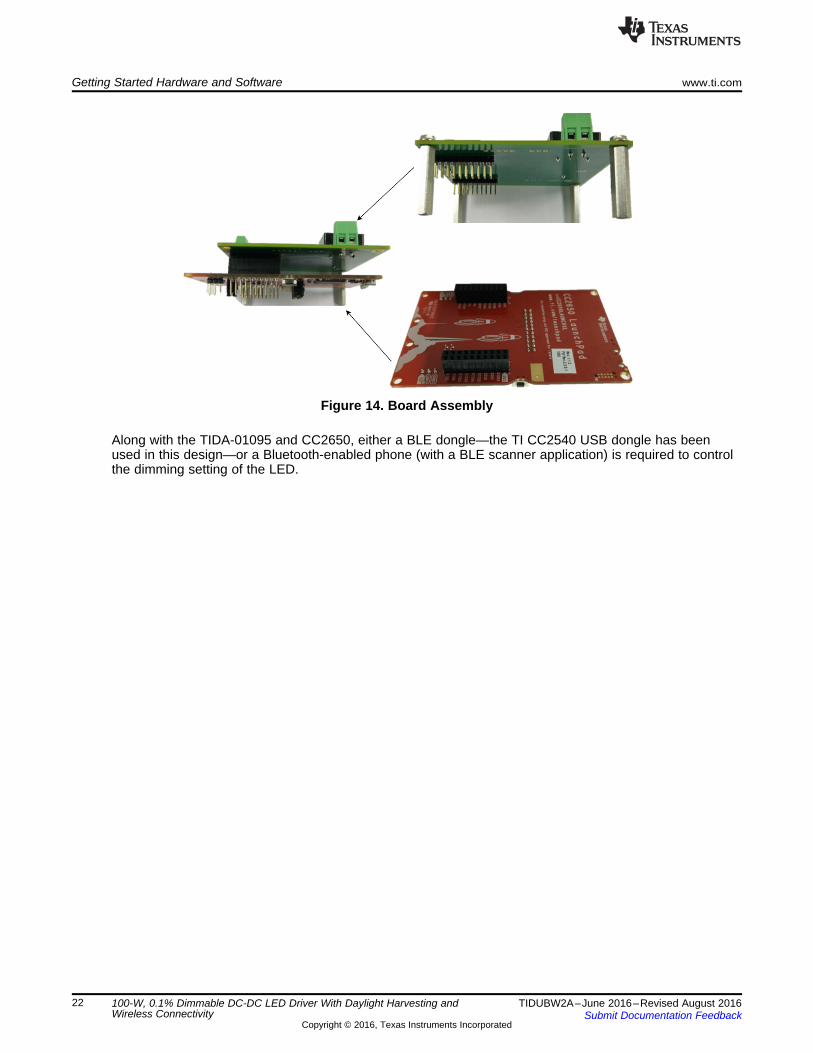
Figure 14. Board Assembly
Along with the TIDA-01095 and CC2650, either a BLE dongle—the TI CC2540 USB dongle has beenused in this design—or a Bluetooth-enabled phone (with a BLE scanner application) is required to controlthe dimming setting of the LED.

www.ti.com Getting Started Hardware and Software
23TIDUBW2A–June 2016–Revised August 2016Submit Documentation Feedback
Copyright © 2016, Texas Instruments Incorporated
100-W, 0.1% Dimmable DC-DC LED Driver With Daylight Harvesting andWireless Connectivity
3.2 Firmware
3.2.1 Compiling Project in CCS™ SoftwareThe provided project files require TI's Code Composer Studio™ (CCS) software (verified with v6) and theBLE software stack (BLE-STACK V2.1.0, which must be downloaded from the BLE software stack archiveat http://www.ti.com/tool/BLE-STACK-ARCHIVE. Any other installed versions of BLE software stack willrequire uninstallation). After installing CCS and BLE Stack, the compilation can be done as follows. Thefollowing instructions assume that CCS and BLE Stack are installed in the directory C:\ti\, the defaultinstallation directory.1. Download the project from <URL>.2. Open CCS and select (create) an existing (new) workspace.3. Import the example project SimpleBLEPeripheral from
C:\ti\simplelink\ble_cc26xx_2_01_01_44627\Projects\ble\SimpleBLEPeripheral\CC26xx\CCS\SimpleBLEPeripheral.
4. Import the example project SimpleBLEPeripheralStack fromC:\ti\simplelink\ble_cc26xx_2_01_01_44627\Projects\ble\SimpleBLEPeripheral\CC26xx\CCS\SimpleBLEPeripheralStack.
5. Build SimpleBLEPeripheralStack.6. After the SimpleBLEPeripheralStack builds successfully without any error:
• Click on SimpleBLEPeripheral → Application (under the Project Explorer tab), and right-click onsimpleBLEPeripheral.C to select properties. Select Resource on the left pane, and click on Edit toedit the Location. Then, click on File and browse to <directory-name>, and selectsimpleBLEPeripheral.C.
• Similarly, click on SimpleBLEPeripheral → Startup, and right-click on main.C to select properties.Select Resource on the left pane, and click on Edit to edit the Location. Then, click on File andbrowse to <directory-name>, and select main.C.
7. Click on SimpleBLEPeripheral → Startup and open Board.C. Modify the file by adding the following twolines at line number 64 below the comment.64 #if defined(LED_Dimmer_CC2650LP)65 #include "LED_Dimmer/Board.c"
Change the #if directive in the following line (number 66) to #elif. Save the file.8. Right-click on SimpleBLEPeripheral to open properties.
(a) Select the General option in the left pane. Under the Main tab, tick Manage the project’s target-configuration automatically and select Texas Instruments XDS110 USB Debug Probe asConnection.
(b) Click on Include Options under ARM Compiler in the left pane. Click on the Add icon to add thedirectory path. Click on Browse and add the path to the <directory-name>. Similarly, add <directory-name>\LED_Dimmer.
(c) Select Advanced Options → Predefined Symbols from the left pane in the Properties dialogue box.Add the symbol TI_DRIVERS_I2C_INCLUDED (if not already present in the list) by clicking on theAdd icon, typing in TI_DRIVERS_I2C_INCLUDED, and clicking OK. Also, in the same list, modifythe TI_DRIVERS_LCD_INCLUDED entry (if present) by clicking on the Edit icon and typingxTI_DRIVERS_LCD_INCLUDED.
(d) Finally, click OK to close the Properties dialogue box.9. Right-click on SimpleBLEPeripheral → Drivers and select New → Folder. Click on Advanced, and then
Link to alternate location (Linked Folder). Browse to <directory-name>\i2c and Finish.10. Right-click on SimpleBLEPeripheral and navigate to Folder under New to create a new folder. Leave
the default parent folder SimpleBLEPeripheral unchanged, type in the Folder Name as LEDService,and click OK.
11. Right-click on SimpleBLEPeripheral and select Add Files.12. Navigate to <directory-name>\LED_Dimmer. Select all the .C files except Board.C. Select Copy Files
in the next dialogue box and click OK. Move all the added files to LEDService by first selecting all thefiles and then right-clicking to select Move to SimpleBLEPeripheral → LEDService.
Getting Started Hardware and Software www.ti.com
24 TIDUBW2A–June 2016–Revised August 2016Submit Documentation Feedback
Copyright © 2016, Texas Instruments Incorporated
100-W, 0.1% Dimmable DC-DC LED Driver With Daylight Harvesting andWireless Connectivity
13. Right-click on SimpleBLEPeripheral and Clean Project.14. Build the project.
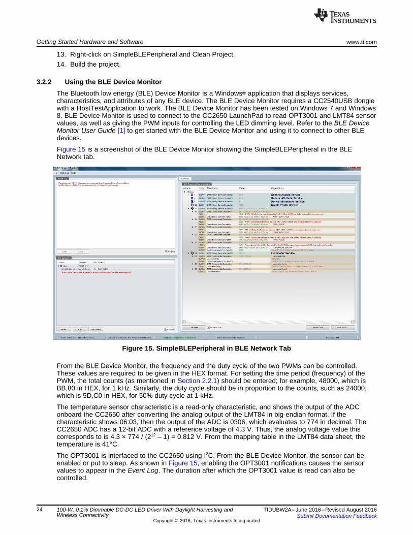
3.2.2 Using the BLE Device MonitorThe Bluetooth low energy (BLE) Device Monitor is a Windows® application that displays services,characteristics, and attributes of any BLE device. The BLE Device Monitor requires a CC2540USB donglewith a HostTestApplication to work. The BLE Device Monitor has been tested on Windows 7 and Windows8. BLE Device Monitor is used to connect to the CC2650 LaunchPad to read OPT3001 and LMT84 sensorvalues, as well as giving the PWM inputs for controlling the LED dimming level. Refer to the BLE DeviceMonitor User Guide [1] to get started with the BLE Device Monitor and using it to connect to other BLEdevices.
Figure 15 is a screenshot of the BLE Device Monitor showing the SimpleBLEPeripheral in the BLENetwork tab.
Figure 15. SimpleBLEPeripheral in BLE Network Tab
From the BLE Device Monitor, the frequency and the duty cycle of the two PWMs can be controlled.These values are required to be given in the HEX format. For setting the time period (frequency) of thePWM, the total counts (as mentioned in Section 2.2.1) should be entered; for example, 48000, which isBB,80 in HEX, for 1 kHz. Similarly, the duty cycle should be in proportion to the counts, such as 24000,which is 5D,C0 in HEX, for 50% duty cycle at 1 kHz.
The temperature sensor characteristic is a read-only characteristic, and shows the output of the ADConboard the CC2650 after converting the analog output of the LMT84 in big-endian format. If thecharacteristic shows 06:03, then the output of the ADC is 0306, which evaluates to 774 in decimal. TheCC2650 ADC has a 12-bit ADC with a reference voltage of 4.3 V. Thus, the analog voltage value thiscorresponds to is 4.3 × 774 / (212 – 1) = 0.812 V. From the mapping table in the LMT84 data sheet, thetemperature is 41°C.
The OPT3001 is interfaced to the CC2650 using I2C. From the BLE Device Monitor, the sensor can beenabled or put to sleep. As shown in Figure 15, enabling the OPT3001 notifications causes the sensorvalues to appear in the Event Log. The duration after which the OPT3001 value is read can also becontrolled.
VIADJ (V)
I OU
T (
A)
0 0.2 0.4 0.6 0.8 1 1.2 1.4 1.60
0.5
1
1.5
2
2.5
3
D002
www.ti.com Test Data (With 60-V MOSFETs)
25TIDUBW2A–June 2016–Revised August 2016Submit Documentation Feedback
Copyright © 2016, Texas Instruments Incorporated
100-W, 0.1% Dimmable DC-DC LED Driver With Daylight Harvesting andWireless Connectivity
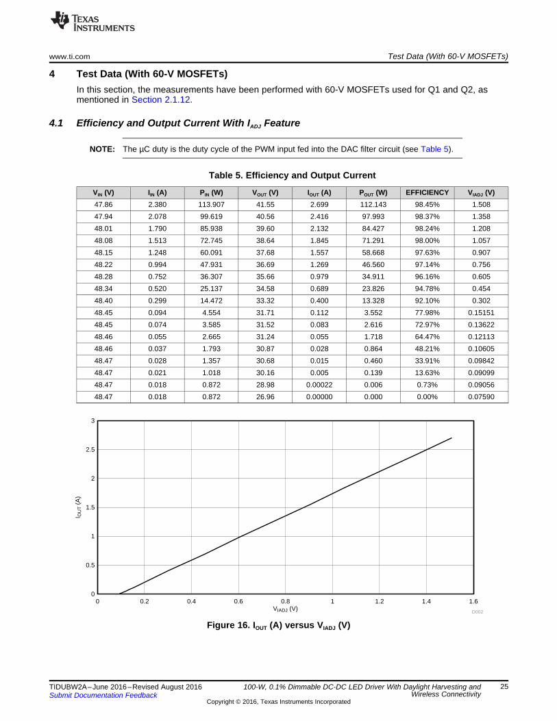
4 Test Data (With 60-V MOSFETs)In this section, the measurements have been performed with 60-V MOSFETs used for Q1 and Q2, asmentioned in Section 2.1.12.
4.1 Efficiency and Output Current With IADJ Feature
NOTE: The µC duty is the duty cycle of the PWM input fed into the DAC filter circuit (see Table 5).
Table 5. Efficiency and Output Current
VIN (V) IIN (A) PIN (W) VOUT (V) IOUT (A) POUT (W) EFFICIENCY VIADJ (V)47.86 2.380 113.907 41.55 2.699 112.143 98.45% 1.50847.94 2.078 99.619 40.56 2.416 97.993 98.37% 1.35848.01 1.790 85.938 39.60 2.132 84.427 98.24% 1.20848.08 1.513 72.745 38.64 1.845 71.291 98.00% 1.05748.15 1.248 60.091 37.68 1.557 58.668 97.63% 0.90748.22 0.994 47.931 36.69 1.269 46.560 97.14% 0.75648.28 0.752 36.307 35.66 0.979 34.911 96.16% 0.60548.34 0.520 25.137 34.58 0.689 23.826 94.78% 0.45448.40 0.299 14.472 33.32 0.400 13.328 92.10% 0.30248.45 0.094 4.554 31.71 0.112 3.552 77.98% 0.1515148.45 0.074 3.585 31.52 0.083 2.616 72.97% 0.1362248.46 0.055 2.665 31.24 0.055 1.718 64.47% 0.1211348.46 0.037 1.793 30.87 0.028 0.864 48.21% 0.1060548.47 0.028 1.357 30.68 0.015 0.460 33.91% 0.0984248.47 0.021 1.018 30.16 0.005 0.139 13.63% 0.0909948.47 0.018 0.872 28.98 0.00022 0.006 0.73% 0.0905648.47 0.018 0.872 26.96 0.00000 0.000 0.00% 0.07590
Figure 16. IOUT (A) versus VIADJ (V)
PC PWM Count for IADJ Ref PWM DAC
I OU
T (
mA
)
4818 4820 4822 4824 4826 4828 4830 4832997.5
998
998.5
999
999.5
1000
1000.5
1001
D004
IOUT (A)
Effi
cien
cy
0 0.5 1 1.5 2 2.5 30
10%
20%
30%
40%
50%
60%
70%
80%
90%
100%
D003
Test Data (With 60-V MOSFETs) www.ti.com
26 TIDUBW2A–June 2016–Revised August 2016Submit Documentation Feedback
Copyright © 2016, Texas Instruments Incorporated
100-W, 0.1% Dimmable DC-DC LED Driver With Daylight Harvesting andWireless Connectivity
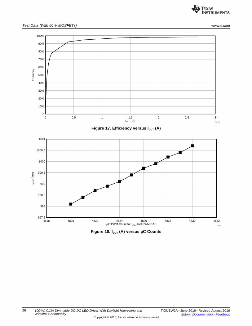
Figure 17. Efficiency versus IOUT (A)
Figure 18. IOUT (A) versus µC Counts
UDIM Duty Cycle
I OU
T (
A)
0 20% 40% 60% 80% 100%0
0.5
1
1.5
2
2.5
3
D005
www.ti.com Test Data (With 60-V MOSFETs)
27TIDUBW2A–June 2016–Revised August 2016Submit Documentation Feedback
Copyright © 2016, Texas Instruments Incorporated
100-W, 0.1% Dimmable DC-DC LED Driver With Daylight Harvesting andWireless Connectivity
4.2 Efficiency and Output Current With UDIM Feature
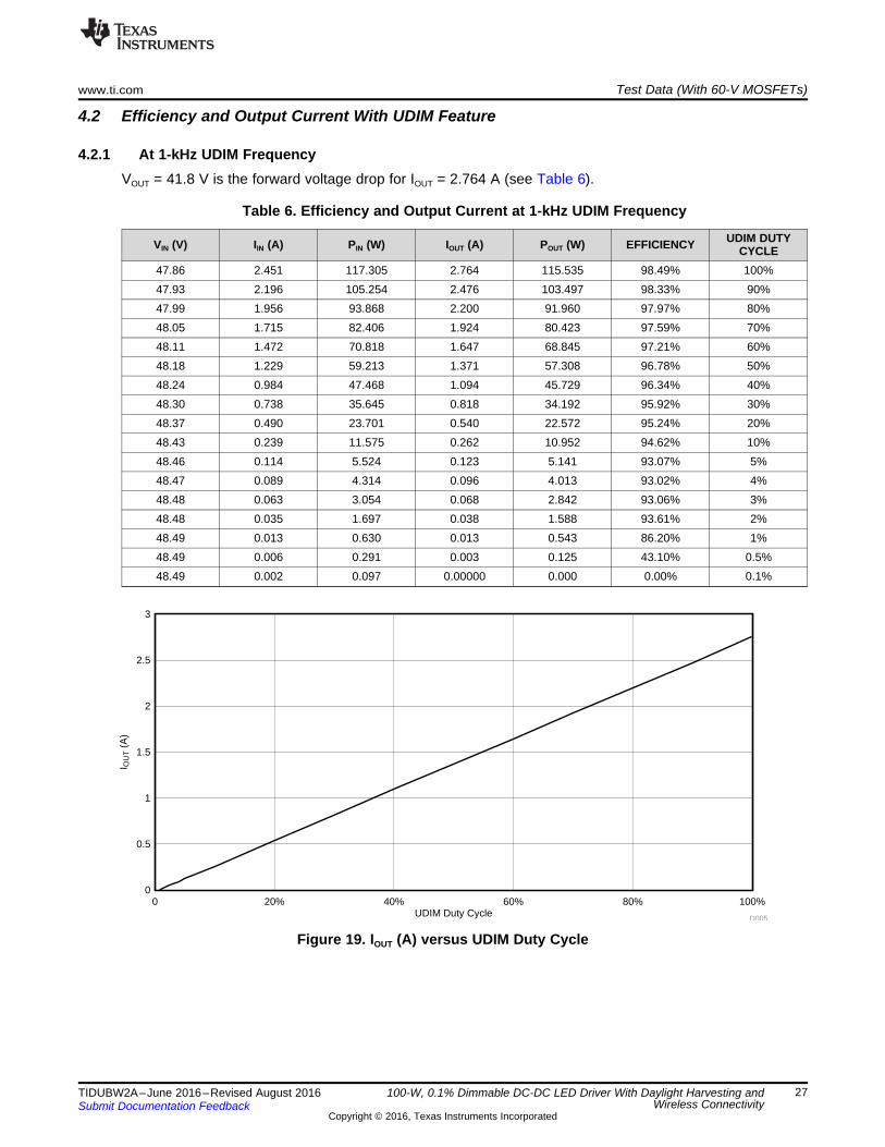
4.2.1 At 1-kHz UDIM FrequencyVOUT = 41.8 V is the forward voltage drop for IOUT = 2.764 A (see Table 6).
Table 6. Efficiency and Output Current at 1-kHz UDIM Frequency
VIN (V) IIN (A) PIN (W) IOUT (A) POUT (W) EFFICIENCY UDIM DUTYCYCLE
47.86 2.451 117.305 2.764 115.535 98.49% 100%47.93 2.196 105.254 2.476 103.497 98.33% 90%47.99 1.956 93.868 2.200 91.960 97.97% 80%48.05 1.715 82.406 1.924 80.423 97.59% 70%48.11 1.472 70.818 1.647 68.845 97.21% 60%48.18 1.229 59.213 1.371 57.308 96.78% 50%48.24 0.984 47.468 1.094 45.729 96.34% 40%48.30 0.738 35.645 0.818 34.192 95.92% 30%48.37 0.490 23.701 0.540 22.572 95.24% 20%48.43 0.239 11.575 0.262 10.952 94.62% 10%48.46 0.114 5.524 0.123 5.141 93.07% 5%48.47 0.089 4.314 0.096 4.013 93.02% 4%48.48 0.063 3.054 0.068 2.842 93.06% 3%48.48 0.035 1.697 0.038 1.588 93.61% 2%48.49 0.013 0.630 0.013 0.543 86.20% 1%48.49 0.006 0.291 0.003 0.125 43.10% 0.5%48.49 0.002 0.097 0.00000 0.000 0.00% 0.1%
Figure 19. IOUT (A) versus UDIM Duty Cycle
IOUT (A)
Effi
cien
cy
0 0.5 1 1.5 2 2.5 340%
50%
60%
70%
80%
90%
100%
D006
Test Data (With 60-V MOSFETs) www.ti.com
28 TIDUBW2A–June 2016–Revised August 2016Submit Documentation Feedback
Copyright © 2016, Texas Instruments Incorporated
100-W, 0.1% Dimmable DC-DC LED Driver With Daylight Harvesting andWireless Connectivity
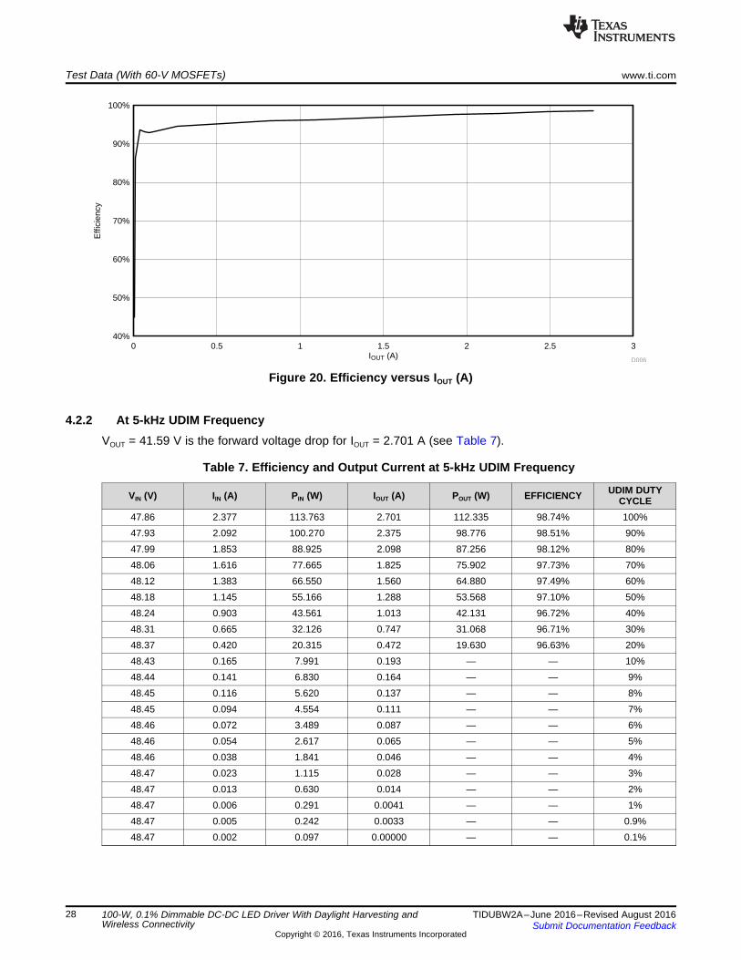
Figure 20. Efficiency versus IOUT (A)
4.2.2 At 5-kHz UDIM FrequencyVOUT = 41.59 V is the forward voltage drop for IOUT = 2.701 A (see Table 7).
Table 7. Efficiency and Output Current at 5-kHz UDIM Frequency
VIN (V) IIN (A) PIN (W) IOUT (A) POUT (W) EFFICIENCY UDIM DUTYCYCLE
47.86 2.377 113.763 2.701 112.335 98.74% 100%47.93 2.092 100.270 2.375 98.776 98.51% 90%47.99 1.853 88.925 2.098 87.256 98.12% 80%48.06 1.616 77.665 1.825 75.902 97.73% 70%48.12 1.383 66.550 1.560 64.880 97.49% 60%48.18 1.145 55.166 1.288 53.568 97.10% 50%48.24 0.903 43.561 1.013 42.131 96.72% 40%48.31 0.665 32.126 0.747 31.068 96.71% 30%48.37 0.420 20.315 0.472 19.630 96.63% 20%48.43 0.165 7.991 0.193 — — 10%48.44 0.141 6.830 0.164 — — 9%48.45 0.116 5.620 0.137 — — 8%48.45 0.094 4.554 0.111 — — 7%48.46 0.072 3.489 0.087 — — 6%48.46 0.054 2.617 0.065 — — 5%48.46 0.038 1.841 0.046 — — 4%48.47 0.023 1.115 0.028 — — 3%48.47 0.013 0.630 0.014 — — 2%48.47 0.006 0.291 0.0041 — — 1%48.47 0.005 0.242 0.0033 — — 0.9%48.47 0.002 0.097 0.00000 — — 0.1%
UDIM Duty Cycle
I OU
T (
A)
0 20% 40% 60% 80% 100%0
0.5
1
1.5
2
2.5
3
D008
IOUT (A)
Effi
cien
cy
0 0.5 1 1.5 2 2.5 380%
82%
84%
86%
88%
90%
92%
94%
96%
98%
100%
D007
www.ti.com Test Data (With 60-V MOSFETs)
29TIDUBW2A–June 2016–Revised August 2016Submit Documentation Feedback
Copyright © 2016, Texas Instruments Incorporated
100-W, 0.1% Dimmable DC-DC LED Driver With Daylight Harvesting andWireless Connectivity
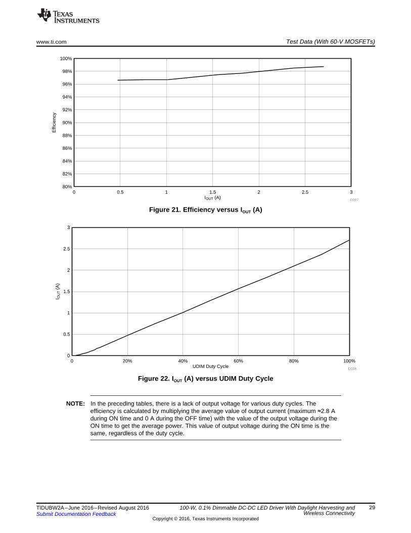
Figure 21. Efficiency versus IOUT (A)
Figure 22. IOUT (A) versus UDIM Duty Cycle
NOTE: In the preceding tables, there is a lack of output voltage for various duty cycles. Theefficiency is calculated by multiplying the average value of output current (maximum ≈2.8 Aduring ON time and 0 A during the OFF time) with the value of the output voltage during theON time to get the average power. This value of output voltage during the ON time is thesame, regardless of the duty cycle.
VIN (V)
Effi
cien
cy
41 42 43 44 45 46 47 48 49 5095%
96%
97%
98%
99%
100%
D009
Test Data (With 60-V MOSFETs) www.ti.com
30 TIDUBW2A–June 2016–Revised August 2016Submit Documentation Feedback
Copyright © 2016, Texas Instruments Incorporated
100-W, 0.1% Dimmable DC-DC LED Driver With Daylight Harvesting andWireless Connectivity
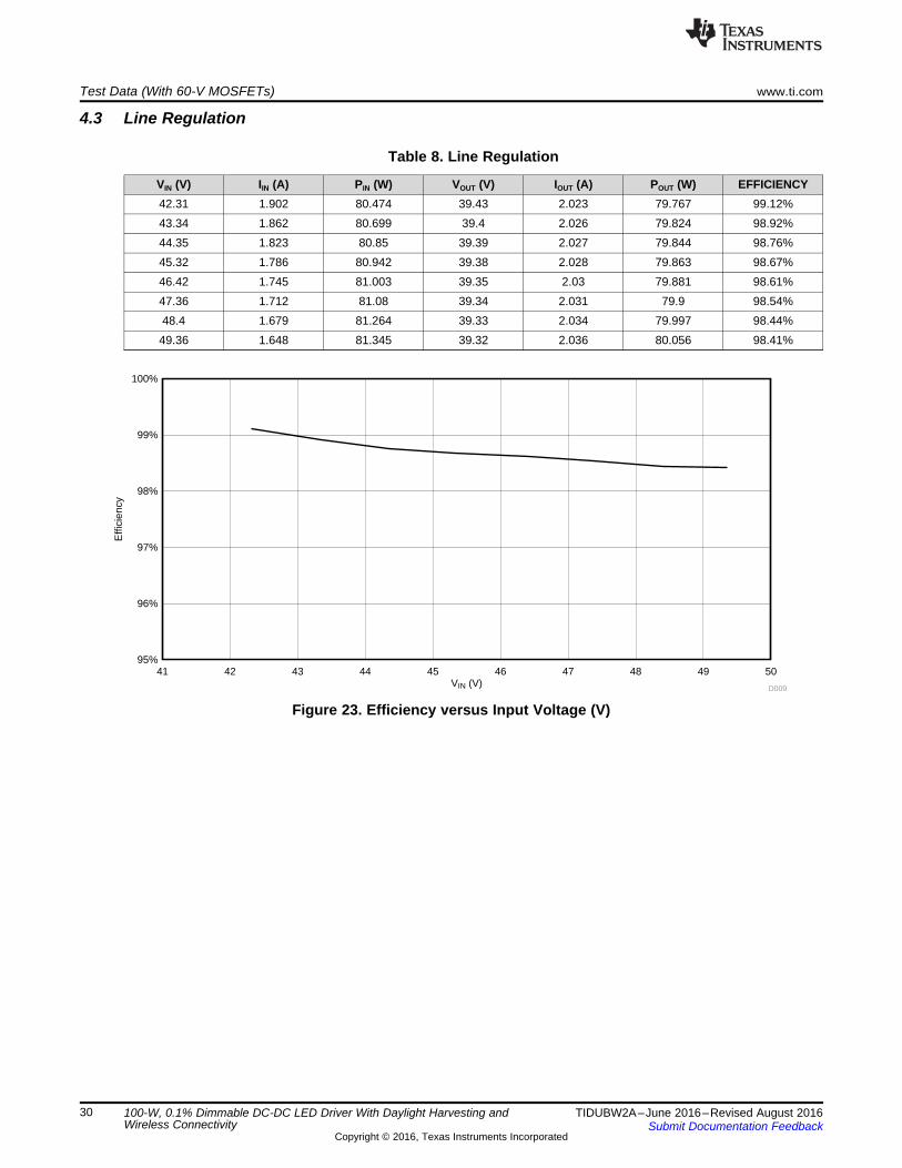
4.3 Line Regulation
Table 8. Line Regulation
VIN (V) IIN (A) PIN (W) VOUT (V) IOUT (A) POUT (W) EFFICIENCY42.31 1.902 80.474 39.43 2.023 79.767 99.12%43.34 1.862 80.699 39.4 2.026 79.824 98.92%44.35 1.823 80.85 39.39 2.027 79.844 98.76%45.32 1.786 80.942 39.38 2.028 79.863 98.67%46.42 1.745 81.003 39.35 2.03 79.881 98.61%47.36 1.712 81.08 39.34 2.031 79.9 98.54%48.4 1.679 81.264 39.33 2.034 79.997 98.44%49.36 1.648 81.345 39.32 2.036 80.056 98.41%
Figure 23. Efficiency versus Input Voltage (V)
IOUT (A)
Illum
inan
ce (
Lux)
0 0.5 1 1.5 2 2.5 30
10000
20000
30000
40000
50000
60000
70000
80000
D010
www.ti.com Test Data (With 60-V MOSFETs)
31TIDUBW2A–June 2016–Revised August 2016Submit Documentation Feedback
Copyright © 2016, Texas Instruments Incorporated
100-W, 0.1% Dimmable DC-DC LED Driver With Daylight Harvesting andWireless Connectivity
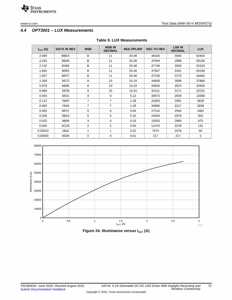
4.4 OPT3001 – LUX Measurements
Table 9. LUX Measurements
IOUT (A) DATA IN HEX MSB MSB INDECIMAL MULTIPLIER DEC TO HEX LSB IN
DECIMAL LUX
2.699 BBEA B 11 20.48 48106 3050 624642.416 BB48 B 11 20.48 47944 2888 591462.132 BA85 B 11 20.48 47749 2693 551531.845 B993 B 11 20.48 47507 2451 501961.557 B87C B 11 20.48 47228 2172 444831.269 AE72 A 10 10.24 44658 3698 378680.979 AB9E A 10 10.24 43934 2974 304540.689 A87B A 10 10.24 43131 2171 222310.400 9A31 9 9 5.12 39473 2609 133580.112 7BAF 7 7 1.28 31663 2991 38280.083 78A9 7 7 1.28 30889 2217 28380.055 6B7C 6 6 0.64 27516 2940 18820.028 5BA3 5 5 0.32 23459 2979 9530.015 4B99 4 4 0.16 19353 2969 4750.005 2CCE 2 2 0.04 11470 3278 131
0.00022 1Ba2 1 1 0.02 7074 2978 600.00000 00D9 0 0 0.01 217 217 2
Figure 24. Illuminance versus IOUT (A)
Test Data (With 60-V MOSFETs) www.ti.com
32 TIDUBW2A–June 2016–Revised August 2016Submit Documentation Feedback
Copyright © 2016, Texas Instruments Incorporated
100-W, 0.1% Dimmable DC-DC LED Driver With Daylight Harvesting andWireless Connectivity
4.4.1 Conversion From OPT3001 Sensor Reading in HEX to LUXThe HEX reading obtained from the OPT3001 sensor can be converted into LUX as follows.
Example, 4CB1:1. Extract the most significant nibble, four in this example, and calculate LSB_size as:
LSB_size = 0.01 × 24 = 0.16.This nibble may even be A, B, C, D, E, or F, in which case the exponent should be taken as thecorresponding decimal number; that is, 10, 11, 12, 13, 14, and 15, respectively.
2. Convert the remaining three least significant nibbles into decimals and multiply by LSB_size to get theLUX value.CB1h = 3249dLUX = 3249 × 0.16 = 519.84
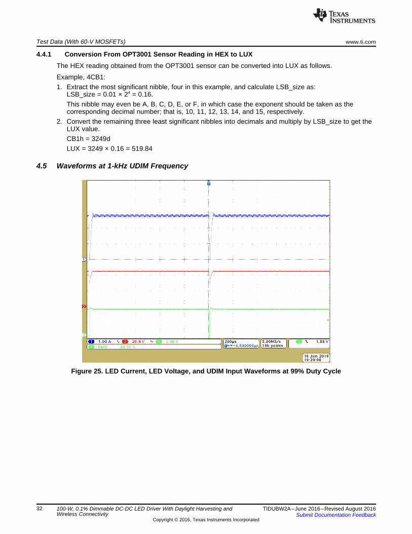
4.5 Waveforms at 1-kHz UDIM Frequency
Figure 25. LED Current, LED Voltage, and UDIM Input Waveforms at 99% Duty Cycle
www.ti.com Test Data (With 60-V MOSFETs)
33TIDUBW2A–June 2016–Revised August 2016Submit Documentation Feedback
Copyright © 2016, Texas Instruments Incorporated
100-W, 0.1% Dimmable DC-DC LED Driver With Daylight Harvesting andWireless Connectivity
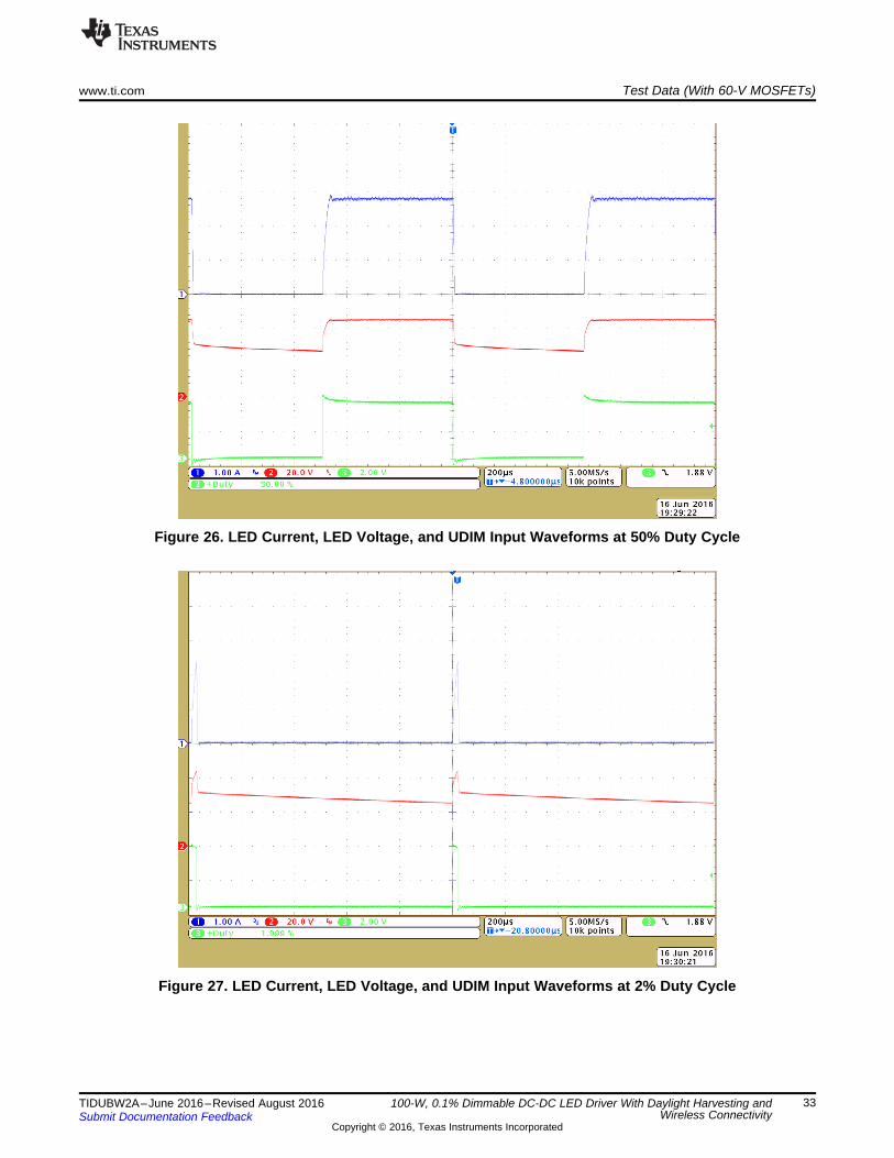
Figure 26. LED Current, LED Voltage, and UDIM Input Waveforms at 50% Duty Cycle
Figure 27. LED Current, LED Voltage, and UDIM Input Waveforms at 2% Duty Cycle
Test Data (With 60-V MOSFETs) www.ti.com
34 TIDUBW2A–June 2016–Revised August 2016Submit Documentation Feedback
Copyright © 2016, Texas Instruments Incorporated
100-W, 0.1% Dimmable DC-DC LED Driver With Daylight Harvesting andWireless Connectivity
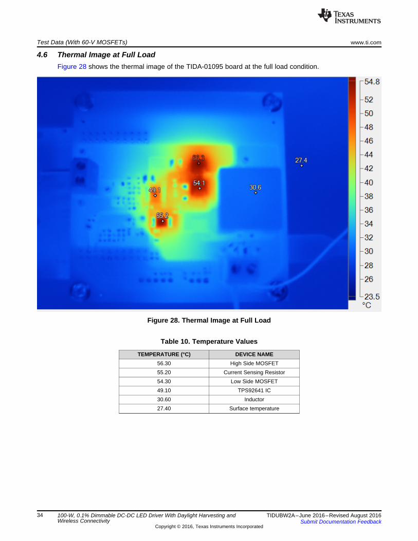
4.6 Thermal Image at Full LoadFigure 28 shows the thermal image of the TIDA-01095 board at the full load condition.
Figure 28. Thermal Image at Full Load
Table 10. Temperature Values
TEMPERATURE (°C) DEVICE NAME56.30 High Side MOSFET55.20 Current Sensing Resistor54.30 Low Side MOSFET49.10 TPS92641 IC30.60 Inductor27.40 Surface temperature
VIADJ (V)
I OU
T (
A)
0 0.5 1 1.5 20
0.5
1
1.5
2
2.5
3
D011
www.ti.com Test Data (With 100-V MOSFETs)
35TIDUBW2A–June 2016–Revised August 2016Submit Documentation Feedback
Copyright © 2016, Texas Instruments Incorporated
100-W, 0.1% Dimmable DC-DC LED Driver With Daylight Harvesting andWireless Connectivity
5 Test Data (With 100-V MOSFETs)In this section, the measurements are done with 100-V MOSFETs used for Q1 and Q2, as mentioned inSection 2.1.12.
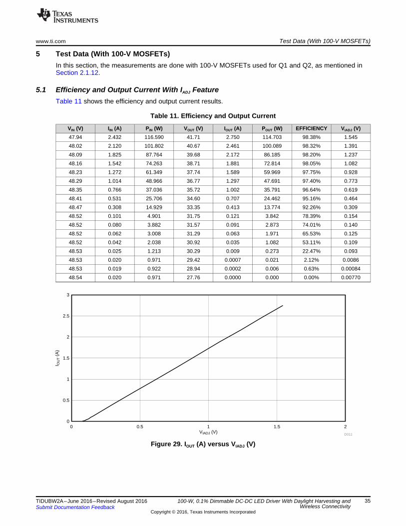
5.1 Efficiency and Output Current With IADJ FeatureTable 11 shows the efficiency and output current results.
Table 11. Efficiency and Output Current
VIN (V) IIN (A) PIN (W) VOUT (V) IOUT (A) POUT (W) EFFICIENCY VIADJ (V)47.94 2.432 116.590 41.71 2.750 114.703 98.38% 1.54548.02 2.120 101.802 40.67 2.461 100.089 98.32% 1.39148.09 1.825 87.764 39.68 2.172 86.185 98.20% 1.23748.16 1.542 74.263 38.71 1.881 72.814 98.05% 1.08248.23 1.272 61.349 37.74 1.589 59.969 97.75% 0.92848.29 1.014 48.966 36.77 1.297 47.691 97.40% 0.77348.35 0.766 37.036 35.72 1.002 35.791 96.64% 0.61948.41 0.531 25.706 34.60 0.707 24.462 95.16% 0.46448.47 0.308 14.929 33.35 0.413 13.774 92.26% 0.30948.52 0.101 4.901 31.75 0.121 3.842 78.39% 0.15448.52 0.080 3.882 31.57 0.091 2.873 74.01% 0.14048.52 0.062 3.008 31.29 0.063 1.971 65.53% 0.12548.52 0.042 2.038 30.92 0.035 1.082 53.11% 0.10948.53 0.025 1.213 30.29 0.009 0.273 22.47% 0.09348.53 0.020 0.971 29.42 0.0007 0.021 2.12% 0.008648.53 0.019 0.922 28.94 0.0002 0.006 0.63% 0.0008448.54 0.020 0.971 27.76 0.0000 0.000 0.00% 0.00770
Figure 29. IOUT (A) versus VIADJ (V)
IOUT (A)
Effi
cien
cy
0 0.5 1 1.5 2 2.5 30
10%
20%
30%
40%
50%
60%
70%
80%
90%
100%
D012
Test Data (With 100-V MOSFETs) www.ti.com
36 TIDUBW2A–June 2016–Revised August 2016Submit Documentation Feedback
Copyright © 2016, Texas Instruments Incorporated
100-W, 0.1% Dimmable DC-DC LED Driver With Daylight Harvesting andWireless Connectivity
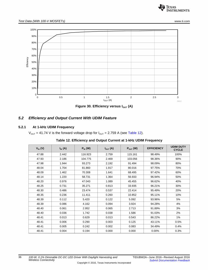
Figure 30. Efficiency versus IOUT (A)
5.2 Efficiency and Output Current With UDIM Feature
5.2.1 At 1-kHz UDIM FrequencyVOUT = 41.74 V is the forward voltage drop for IOUT = 2.759 A (see Table 12).
Table 12. Efficiency and Output Current at 1-kHz UDIM Frequency
VIN (V) IIN (A) PIN (W) IOUT (A) POUT (W) EFFICIENCY UDIM DUTYCYCLE
47.88 2.442 116.923 2.759 115.161 98.49% 100%47.93 2.186 104.775 2.469 103.056 98.36% 90%47.98 1.944 93.273 2.192 91.494 98.09% 80%48.04 1.704 81.860 1.917 80.016 97.75% 70%48.09 1.462 70.308 1.641 68.495 97.42% 60%48.14 1.220 58.731 1.364 56.933 96.94% 50%48.20 0.976 47.043 1.089 45.455 96.62% 40%48.25 0.731 35.271 0.813 33.935 96.21% 30%48.30 0.486 23.474 0.537 22.414 95.49% 20%48.35 0.236 11.411 0.260 10.852 95.11% 10%48.39 0.112 5.420 0.122 5.092 93.96% 5%48.39 0.086 4.162 0.094 3.924 94.28% 4%48.40 0.061 2.952 0.065 2.713 91.89% 3%48.40 0.036 1.742 0.038 1.586 91.03% 2%48.41 0.013 0.629 0.013 0.543 86.22% 1%48.41 0.006 0.290 0.003 0.125 43.11% 0.5%48.41 0.005 0.242 0.002 0.083 34.49% 0.4%48.41 0.004 0.194 0.000 0.000 0.00% 0.3%
UDIM Duty Cycle
I OU
T (
A)
0 20% 40% 60% 80% 100%0
0.5
1
1.5
2
2.5
3
D014
IOUT (A)
Effi
cien
cy
0 0.5 1 1.5 2 2.5 30
10%
20%
30%
40%
50%
60%
70%
80%
90%
100%
D013
www.ti.com Test Data (With 100-V MOSFETs)
37TIDUBW2A–June 2016–Revised August 2016Submit Documentation Feedback
Copyright © 2016, Texas Instruments Incorporated
100-W, 0.1% Dimmable DC-DC LED Driver With Daylight Harvesting andWireless Connectivity
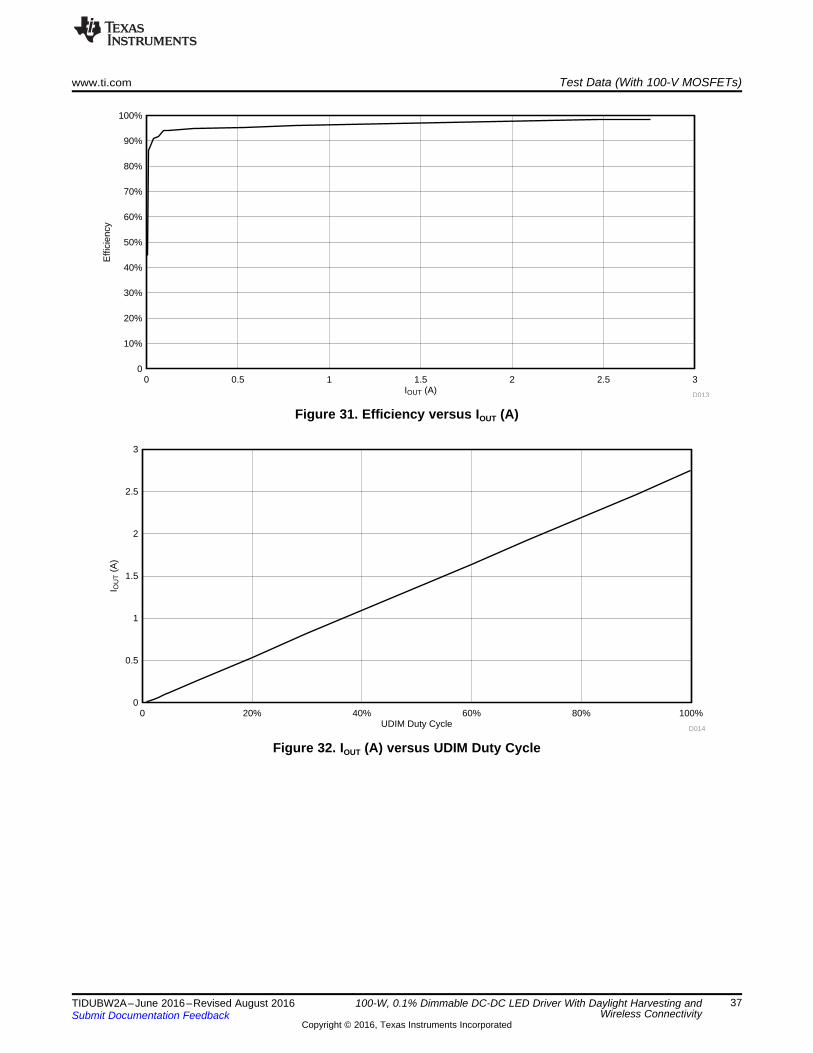
Figure 31. Efficiency versus IOUT (A)
Figure 32. IOUT (A) versus UDIM Duty Cycle
IOUT (A)
Effi
cien
cy
0 0.5 1 1.5 2 2.5 380%
82%
84%
86%
88%
90%
92%
94%
96%
98%
100%
D015
Test Data (With 100-V MOSFETs) www.ti.com
38 TIDUBW2A–June 2016–Revised August 2016Submit Documentation Feedback
Copyright © 2016, Texas Instruments Incorporated
100-W, 0.1% Dimmable DC-DC LED Driver With Daylight Harvesting andWireless Connectivity
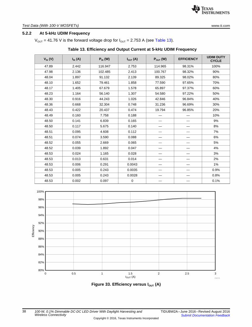
5.2.2 At 5-kHz UDIM FrequencyVOUT = 41.76 V is the forward voltage drop for IOUT = 2.753 A (see Table 13).
Table 13. Efficiency and Output Current at 5-kHz UDIM Frequency
VIN (V) IIN (A) PIN (W) IOUT (A) POUT (W) EFFICIENCY UDIM DUTYCYCLE
47.89 2.442 116.947 2.753 114.965 98.31% 100%47.98 2.136 102.485 2.413 100.767 98.32% 90%48.04 1.897 91.132 2.139 89.325 98.02% 80%48.10 1.652 79.461 1.858 77.590 97.65% 70%48.17 1.405 67.679 1.578 65.897 97.37% 60%48.23 1.164 56.140 1.307 54.580 97.22% 50%48.30 0.916 44.243 1.026 42.846 96.84% 40%48.36 0.668 32.304 0.748 31.236 96.69% 30%48.43 0.422 20.437 0.474 19.794 96.85% 20%48.49 0.160 7.758 0.188 — — 10%48.50 0.141 6.839 0.165 — — 9%48.50 0.117 5.675 0.140 — — 8%48.51 0.095 4.608 0.112 — — 7%48.51 0.074 3.590 0.088 — — 6%48.52 0.055 2.669 0.065 — — 5%48.52 0.039 1.892 0.047 — — 4%48.53 0.024 1.165 0.028 — — 3%48.53 0.013 0.631 0.014 — — 2%48.53 0.006 0.291 0.0043 — — 1%48.53 0.005 0.243 0.0035 — — 0.9%48.53 0.005 0.243 0.0028 — — 0.8%48.53 0.002 0.097 0 — — 0.1%
Figure 33. Efficiency versus IOUT (A)
UDIM Duty Cycle
I OU
T (
A)
0 20% 40% 60% 80% 100%0
0.5
1
1.5
2
2.5
3
D016
www.ti.com Test Data (With 100-V MOSFETs)
39TIDUBW2A–June 2016–Revised August 2016Submit Documentation Feedback
Copyright © 2016, Texas Instruments Incorporated
100-W, 0.1% Dimmable DC-DC LED Driver With Daylight Harvesting andWireless Connectivity
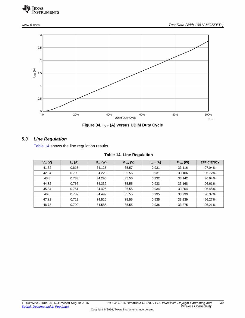
Figure 34. IOUT (A) versus UDIM Duty Cycle
5.3 Line RegulationTable 14 shows the line regulation results.
Table 14. Line Regulation
VIN (V) IIN (A) PIN (W) VOUT (V) IOUT (A) POUT (W) EFFICIENCY41.82 0.816 34.125 35.57 0.931 33.116 97.04%42.84 0.799 34.229 35.56 0.931 33.106 96.72%43.8 0.783 34.295 35.56 0.932 33.142 96.64%44.82 0.766 34.332 35.55 0.933 33.168 96.61%45.84 0.751 34.426 35.55 0.934 33.204 96.45%46.8 0.737 34.492 35.55 0.935 33.239 96.37%47.82 0.722 34.526 35.55 0.935 33.239 96.27%48.78 0.709 34.585 35.55 0.936 33.275 96.21%
VIN (V)
Effi
cien
cy
40 42 44 46 48 50 5295%
96%
97%
98%
99%
100%
D0017
Test Data (With 100-V MOSFETs) www.ti.com
40 TIDUBW2A–June 2016–Revised August 2016Submit Documentation Feedback
Copyright © 2016, Texas Instruments Incorporated
100-W, 0.1% Dimmable DC-DC LED Driver With Daylight Harvesting andWireless Connectivity
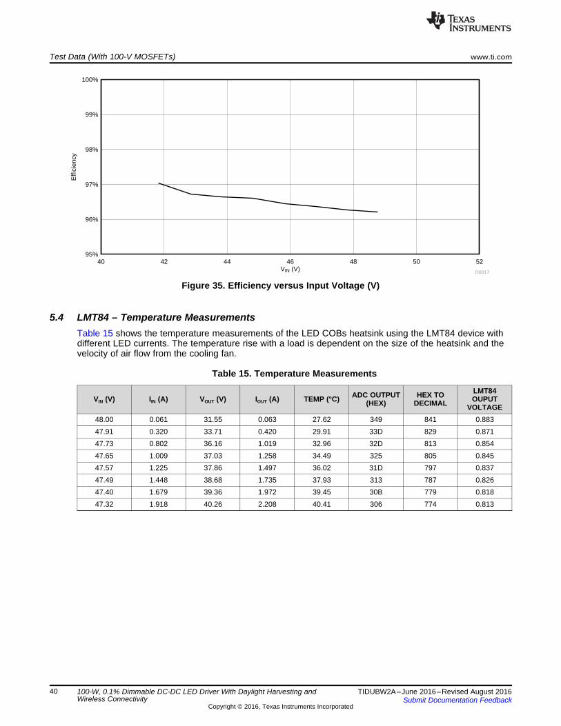
Figure 35. Efficiency versus Input Voltage (V)
5.4 LMT84 – Temperature MeasurementsTable 15 shows the temperature measurements of the LED COBs heatsink using the LMT84 device withdifferent LED currents. The temperature rise with a load is dependent on the size of the heatsink and thevelocity of air flow from the cooling fan.
Table 15. Temperature Measurements
VIN (V) IIN (A) VOUT (V) IOUT (A) TEMP (°C) ADC OUTPUT(HEX)
HEX TODECIMAL
LMT84OUPUT
VOLTAGE48.00 0.061 31.55 0.063 27.62 349 841 0.88347.91 0.320 33.71 0.420 29.91 33D 829 0.87147.73 0.802 36.16 1.019 32.96 32D 813 0.85447.65 1.009 37.03 1.258 34.49 325 805 0.84547.57 1.225 37.86 1.497 36.02 31D 797 0.83747.49 1.448 38.68 1.735 37.93 313 787 0.82647.40 1.679 39.36 1.972 39.45 30B 779 0.81847.32 1.918 40.26 2.208 40.41 306 774 0.813
IOUT (A)
Tem
pera
ture
(qC
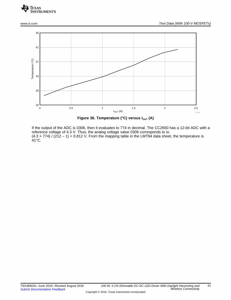
)
0 0.5 1 1.5 2 2.525
29
33
37
41
45
D018
www.ti.com Test Data (With 100-V MOSFETs)
41TIDUBW2A–June 2016–Revised August 2016Submit Documentation Feedback
Copyright © 2016, Texas Instruments Incorporated
100-W, 0.1% Dimmable DC-DC LED Driver With Daylight Harvesting andWireless Connectivity
Figure 36. Temperature (°C) versus IOUT (A)
If the output of the ADC is 0306, then it evaluates to 774 in decimal. The CC2650 has a 12-bit ADC with areference voltage of 4.3 V. Thus, the analog voltage value 0306 corresponds to is:(4.3 × 774) / (212 – 1) = 0.812 V. From the mapping table in the LMT84 data sheet, the temperature is41°C.
Design Files www.ti.com
42 TIDUBW2A–June 2016–Revised August 2016Submit Documentation Feedback
Copyright © 2016, Texas Instruments Incorporated
100-W, 0.1% Dimmable DC-DC LED Driver With Daylight Harvesting andWireless Connectivity
6 Design Files
6.1 SchematicsTo download the schematics, see the design files at TIDA-010905.
6.2 Bill of MaterialsTo download the bill of materials (BOM), see the design files at TIDA-010905.
6.3 PCB Layout RecommendationsThe performance of any switching converter depends as much upon the layout of the PCB as thecomponent selection. Follow a few simple guidelines to maximize noise rejection and minimize thegeneration of EMI within the circuit.
Discontinuous currents are the most likely to generate EMI, therefore take care when routing these paths.The main path for discontinuous current in the TPS92640 and TPS92641 buck converters contains theinput capacitor (CIN), the low-side MOSFET (QLS), and the high-side MOSFET (QHS). This loop shouldbe kept as small as possible, and the connections between all three components should be short and thickto minimize parasitic inductance. In particular, the switch node (where L, QLS, and QHS connect) shouldbe just large enough to connect the components without excessive heating from the current it carries. Thecurrent sense trace (CS pin) should be run along with a ground plane or have differential traces run for CSand ground.
In some applications, the LED or LED array can be far away (several inches or more) from the circuit, oron a separate PCB connected by a wiring harness. When an output capacitor is used and the LED arrayis large or separated from the rest of the converter, the output capacitor should be placed close to theLEDs to reduce the effects of parasitic inductance on the AC impedance of the capacitor.
6.3.1 Layout PrintsTo download the layer plots, see the design files at TIDA-010905.
6.4 Altium ProjectTo download the Altium project files, see the design files at TIDA-010905.
www.ti.com Design Files
43TIDUBW2A–June 2016–Revised August 2016Submit Documentation Feedback
Copyright © 2016, Texas Instruments Incorporated
100-W, 0.1% Dimmable DC-DC LED Driver With Daylight Harvesting andWireless Connectivity
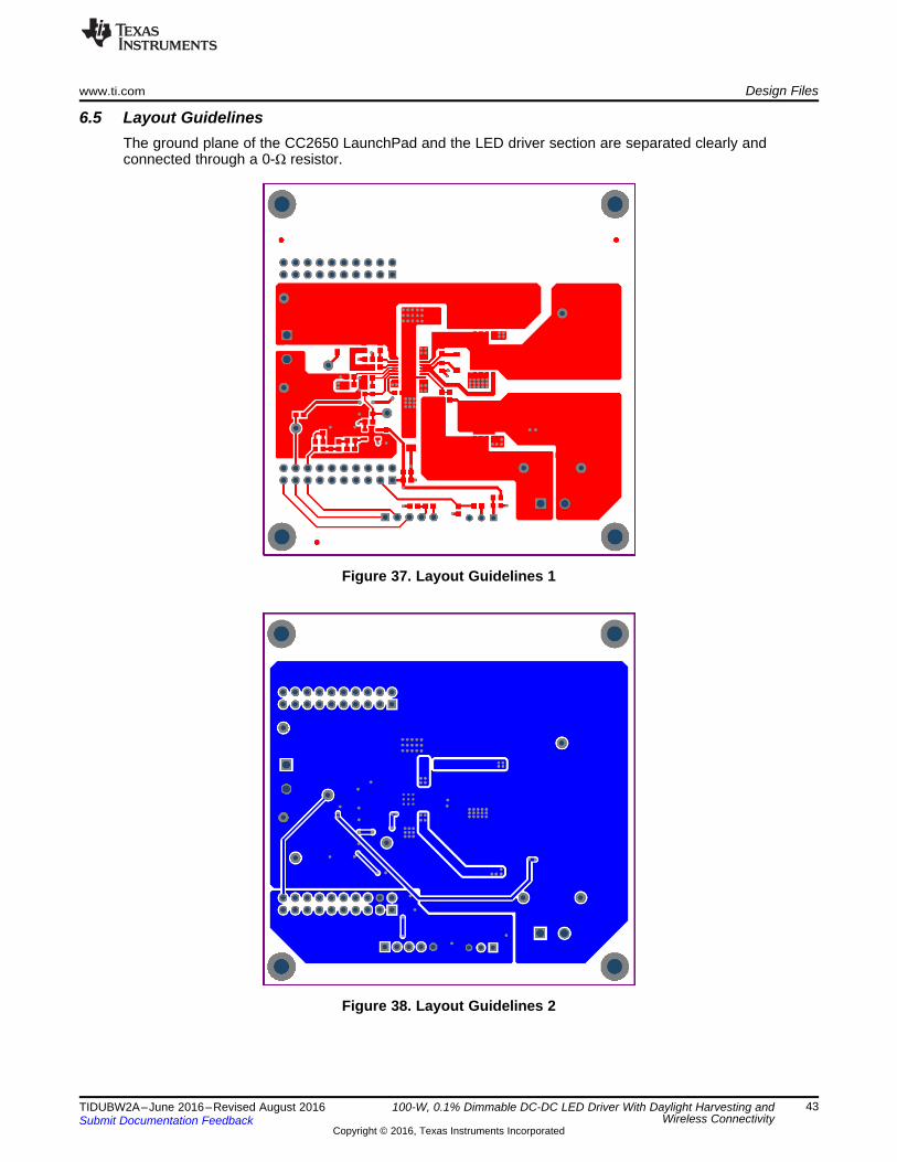
6.5 Layout GuidelinesThe ground plane of the CC2650 LaunchPad and the LED driver section are separated clearly andconnected through a 0-Ω resistor.
Figure 37. Layout Guidelines 1
Figure 38. Layout Guidelines 2
Design Files www.ti.com
44 TIDUBW2A–June 2016–Revised August 2016Submit Documentation Feedback
Copyright © 2016, Texas Instruments Incorporated
100-W, 0.1% Dimmable DC-DC LED Driver With Daylight Harvesting andWireless Connectivity
6.6 Gerber FilesTo download the Gerber files, see the design files at TIDA-010905.
6.7 Assembly DrawingsTo download the assembly drawings, see the design files at TIDA-010905.
7 Software FilesTo download the software files, see the design files at TIDA-010905.
8 References
1. Texas Instruments, BLE Device Monitor User Guide, TI Wiki(http://processors.wiki.ti.com/index.php/BLE_Device_Monitor_User_Guide)
2. Texas Instruments, Dimming Techniques for Switched-Mode LED Drivers, LM3406/LM3409 ApplicationReport (SNVA605)
3. Texas Instruments, Ringing Reduction Techniques for NexFET High Performance MOSFETs,Application Report (SLPA010)
4. Texas Instruments, Microcontroller PWM to 12-Bit Analog Out, TIPD127 User's Guide (TIDU027)5. Texas Instruments, WEBENCH® Design Center, (http://www.ti.com/webench)
9 About the AuthorsSEETHARAMAN DEVENDRAN is a Systems Architect at Texas Instruments, where he is responsible fordeveloping reference design solutions for the industrial segment. Seetharaman brings to this role hisextensive experience in analog and mixed signal system-level design expertise. Seetharaman earned hisBachelor’s degree in Electrical Engineering (BE, EEE) from Thiagarajar College of Engineering, Madurai,India.
MUSTAFA LOKHANDWALA is an undergraduate student at the Indian Institute of Technology Bombay(IITB), where he is pursuing a Bachelor of Technology (BTech) in Electrical Engineering. His areas ofinterest include design and debug of circuits and systems, as well as hardware product development.
VENKATADRI SHANTARAM is a Field Applications Engineer at Texas Instruments, where he isresponsible for supporting customers across various end equipments; primarily supporting customers onTexas Instruments Embedded processors, microcontrollers, and wireless SoCs. Venkatadri earned hisBachelor’s degree in Electrical Engineering (BE, EEE) from The National Institute of Engineering, Mysore,India.

www.ti.com Revision History
45TIDUBW2A–June 2016–Revised August 2016Submit Documentation Feedback
Copyright © 2016, Texas Instruments Incorporated
Revision History
Revision HistoryNOTE: Page numbers for previous revisions may differ from page numbers in the current version.
Changes from Original (June 2016) to A Revision ......................................................................................................... Page
• Changed the design guide from preview to active and added remaining material ............................................... 1

IMPORTANT NOTICE FOR TI REFERENCE DESIGNS
Texas Instruments Incorporated (‘TI”) reference designs are solely intended to assist designers (“Designer(s)”) who are developing systemsthat incorporate TI products. TI has not conducted any testing other than that specifically described in the published documentation for aparticular reference design.TI’s provision of reference designs and any other technical, applications or design advice, quality characterization, reliability data or otherinformation or services does not expand or otherwise alter TI’s applicable published warranties or warranty disclaimers for TI products, andno additional obligations or liabilities arise from TI providing such reference designs or other items.TI reserves the right to make corrections, enhancements, improvements and other changes to its reference designs and other items.Designer understands and agrees that Designer remains responsible for using its independent analysis, evaluation and judgment indesigning Designer’s systems and products, and has full and exclusive responsibility to assure the safety of its products and compliance ofits products (and of all TI products used in or for such Designer’s products) with all applicable regulations, laws and other applicablerequirements. Designer represents that, with respect to its applications, it has all the necessary expertise to create and implementsafeguards that (1) anticipate dangerous consequences of failures, (2) monitor failures and their consequences, and (3) lessen thelikelihood of failures that might cause harm and take appropriate actions. Designer agrees that prior to using or distributing any systemsthat include TI products, Designer will thoroughly test such systems and the functionality of such TI products as used in such systems.Designer may not use any TI products in life-critical medical equipment unless authorized officers of the parties have executed a specialcontract specifically governing such use. Life-critical medical equipment is medical equipment where failure of such equipment would causeserious bodily injury or death (e.g., life support, pacemakers, defibrillators, heart pumps, neurostimulators, and implantables). Suchequipment includes, without limitation, all medical devices identified by the U.S. Food and Drug Administration as Class III devices andequivalent classifications outside the U.S.Designers are authorized to use, copy and modify any individual TI reference design only in connection with the development of endproducts that include the TI product(s) identified in that reference design. HOWEVER, NO OTHER LICENSE, EXPRESS OR IMPLIED, BYESTOPPEL OR OTHERWISE TO ANY OTHER TI INTELLECTUAL PROPERTY RIGHT, AND NO LICENSE TO ANY TECHNOLOGY ORINTELLECTUAL PROPERTY RIGHT OF TI OR ANY THIRD PARTY IS GRANTED HEREIN, including but not limited to any patent right,copyright, mask work right, or other intellectual property right relating to any combination, machine, or process in which TI products orservices are used. Information published by TI regarding third-party products or services does not constitute a license to use such productsor services, or a warranty or endorsement thereof. Use of the reference design or other items described above may require a license from athird party under the patents or other intellectual property of the third party, or a license from TI under the patents or other intellectualproperty of TI.TI REFERENCE DESIGNS AND OTHER ITEMS DESCRIBED ABOVE ARE PROVIDED “AS IS” AND WITH ALL FAULTS. TI DISCLAIMSALL OTHER WARRANTIES OR REPRESENTATIONS, EXPRESS OR IMPLIED, REGARDING THE REFERENCE DESIGNS OR USE OFTHE REFERENCE DESIGNS, INCLUDING BUT NOT LIMITED TO ACCURACY OR COMPLETENESS, TITLE, ANY EPIDEMIC FAILUREWARRANTY AND ANY IMPLIED WARRANTIES OF MERCHANTABILITY, FITNESS FOR A PARTICULAR PURPOSE, AND NON-INFRINGEMENT OF ANY THIRD PARTY INTELLECTUAL PROPERTY RIGHTS.TI SHALL NOT BE LIABLE FOR AND SHALL NOT DEFEND OR INDEMNIFY DESIGNERS AGAINST ANY CLAIM, INCLUDING BUT NOTLIMITED TO ANY INFRINGEMENT CLAIM THAT RELATES TO OR IS BASED ON ANY COMBINATION OF PRODUCTS ASDESCRIBED IN A TI REFERENCE DESIGN OR OTHERWISE. IN NO EVENT SHALL TI BE LIABLE FOR ANY ACTUAL, DIRECT,SPECIAL, COLLATERAL, INDIRECT, PUNITIVE, INCIDENTAL, CONSEQUENTIAL OR EXEMPLARY DAMAGES IN CONNECTION WITHOR ARISING OUT OF THE REFERENCE DESIGNS OR USE OF THE REFERENCE DESIGNS, AND REGARDLESS OF WHETHER TIHAS BEEN ADVISED OF THE POSSIBILITY OF SUCH DAMAGES.TI’s standard terms of sale for semiconductor products (http://www.ti.com/sc/docs/stdterms.htm) apply to the sale of packaged integratedcircuit products. Additional terms may apply to the use or sale of other types of TI products and services.Designer will fully indemnify TI and its representatives against any damages, costs, losses, and/or liabilities arising out of Designer’s non-compliance with the terms and provisions of this Notice.IMPORTANT NOTICE
Mailing Address: Texas Instruments, Post Office Box 655303, Dallas, Texas 75265Copyright © 2016, Texas Instruments Incorporated


![IK QT LED Lighting seminar 20140528 r2.ppt [호환 모드] Lighting seminar_20140528_r2.pdf · High power Constant current LED ... provide uniform and constant current sinks for driving](https://img.pdfslide.tips/doc/110x75/5aa701067f8b9a54748b7536/ik-qt-led-lighting-seminar-20140528-r2ppt-lighting-seminar20140528r2pdfhigh.jpg)