Embed Size (px)
Citation preview

111111111111111111111111111111111111111111111111111111111111111111111111 ll Dl lli USOO8 134 129B2
(12) United States Patent Tokanai et al.
(54) MICROCHANNEL PLATE, GAS PROPORTIONAL COUNTER AND IMAGING DEVICE
(75) Inventors: Fuyuki Tokanai, Yamagata (JP); Takahisa Sakurai, Yamagata (JP); Shuichi Gunji, Yamagata (JP); Takayuki Sumiyoshi, Ibaraki (JP); Teruyuki Okada, Shizuoka (JP); Tetsuro Endo, Shizuoka (JP); Yoshio Fujita, Shizuoka (JP)
(73) Assignee: Japan Science and Technology Agency, Saitama (JP)
(*) Notice: Subject to any disclaimer, the term of this patent is extended or adjusted under 35 U.S.C. 154(b) by 490 days.
(21) Appl. No.: 11/989,537
(22) PCT Filed: Jul. 28, 2006
(86) PCT No.: PCT/JP2006/315062
§ 371 (c)(1), (2), (4) Date: Aug. 19, 2009
(87) PCT Pub. No.: W02007/013630
PCT Pub. Date: Feb. 1, 2007
(65) Prior Publication Data
US 2011/0155919 Al Jun. 30, 2011
(30) Foreign Application Priority Data
Jul. 29, 2005 (JP) ................................. 2005-221722
(51) Int. Cl. GO1T 1/00 (2006.01)
(52) U.S. Cl . .................................... 250/361 R; 250/362
(10) Patent No.: US 8,134,129 B2 (45) Date of Patent: Mar. 13, 2012
(58) Field of Classification Search .............. 250/361 R, 250/362, 367, 368, 370.01, 370.09, 389
See application file for complete search history.
(56) References Cited
U.S. PATENT DOCUMENTS
4,825,118 A 4/1989 Kyushima ..................... 313/104
6,333,506 BI 12/2001 Francke et al.
FOREIGN PATENT DOCUMENTS
CN 1349613 A 5/2002 JP S62-058536 A 3/1987 JP 05-074406 3/1993 JP 09-063533 A 3/1997 JP 2002-543573 12/2002 JP 2004-241298 8/2004 JP 2005-032634 2/2005
(Continued)
OTHER PUBLICATIONS
H. Sakurai, et al. "A new type of proportional counter using a capil-lary plate", Nuclear Instruments and Methods in Physics Research A 374 (1996) 341-344.
(Continued)
Primary Examiner Mark R Gaworecki (74) Attorney, Agent, or Firm Morgan, Lewis & Bockius LLP
(57) ABSTRACT
An object of the present invention is to provide a microchan-nel plate having excellent characteristics which enable to attain both high luminance and high resolution at the same time, a gas proportional counter using such a microchannel plate and an imaging device. The microchannel plate accord-ing to the present invention comprises a base body provided with a plurality of through holes (13) and having an insulating property, and is arranged in a gas atmosphere mainly contain-ing an inert gas to constitute a proportional counter. The base body has photoelectric converter portions (1a, 1b) formed on at least inner walls of the plurality of through holes (13).
8 Claims, 21 Drawing Sheets
I

US 8,134,129 B2 Page 2
FOREIGN PATENT DOCUMENTS
WO WO 00/67043 11/2000 WO WO 2004 049382 A2 6/2004
OTHER PUBLICATIONS
H. Sakurai, et al. "Detection of Photoabsorption Point With Capillary Imaging Gas Proportional Counter", IEEE Transactions on Nuclear
Science, vol. 49, No. 3, Jun. 2002. M. Tsukahara, et al. "The Development of a New Type of Imaging X-Ray Detector with a Capillary Plate", IEEE Transactions on Nuclear Science vol. 44, No. 3, Jun. 1997. H. Sakurai, et al. "The Form of X-ray Photoelectron Tracks in a Capillary Gas Proportional Counter" IEEE Transactions on Nuclear Science, vol. 46, No. 3, Jun. 1999. H. Sakurai "Imaging Gas Proportional Counter with Capillary Plate" vol. 25, No. 1 (1999).
T. Masuda, et al. "Optical Imaging Capillary Gas Proportional Counter With Penning Mixtures" IEEE Transactions on Nuclear Science, vol. 49, No. 2, Apr. 2002. F. Sauli "GEM: A new concept for electreon amplification in gas detectors" Nuclear Instruments and Methods in Physics Research A 386 (1997) 531-534. F.A.F. Fraga, et al. "Quality control of GEM detectors using scintil-lation techniques" Nuclear Instruments and Methods in Physics Research A 442 (2000) 417-422. D. Mormann, et al. "GEM-based gaseous photomultipliers for UV and visible photon imaging" Nuclear Instruments and Methods in Physics Research Z 504 (2003) 93-98. H. Sakurai, et al. "Characteristics of capillary gas proportional counter", SPIE vol. 2806, pp. 569-576 (Publication Date: 1996). H. Sakurai, et al. "New Type of Imaging X-Ray Detector Using A Capillary Plate" SPIE vol. 3114, pp. 481-487 (Publication Date: 1997). Yuji Nishi, et al. "Development of a hybrid MSGC with a conductive capillary plate" SPIE, vol. 3774, pp. 87-96 (Publication Date: 1999).

U.S. Patent
Mar. 13, 2012 Sheet 1 of 21 US 8,134,129 B2
FIG. 1
11
FIG. 2
1/1 11
0L

4o ill 1a 13
U.S. Patent Mar. 13, 2012 Sheet 2 of 21 US 8,134,129 B2
FIG. 3
T 4{VP
— vtop
Lt0p
1b
— Vbot

U.S. Patent Mar. 13, 2012 Sheet 3 of 21 US 8,134,129 B2
FIG. 4
200
71(1

U.S. Patent Mar. 13, 2012 Sheet 4 of 21 US 8,134,129 B2
FIG. 5
a C1
tO r CV
ZI
C)

Contours of V La=25tm -3
*10 50
45
N 40
35
30
25
20
15
10
5
W Lv
P
U.S. Patent Mar. 13, 2012 Sheet 5 of 21 US 8,134,129 B2
Viewing plane: y0.0026 13 -x Axis [cm]

*10
E u
N
U.S. Patent Mar. 13, 2012 Sheet 6 of 21 US 8,134,129 B2
FIG.7
Contours of V
50
tiZ'81~, "_48.24 ,
:$Z.$.. 48.24—~--
45 .. ...:...
48.48 , 48.48—~---
40 48,72 4° 72
48.96 48.96 . . . . . . . . . . . . . . . .
. . . . . . . . . . . . . . . .
t~b'6t~ 49.44 ' tr6ti 49.44—*—~-
30 ;....;... .. .;........ .. ..... . 49.68 49.68
Z6'6ii 49.92---^---~--~ b--=-- ---x-49.92-- -. _ .Z6'6 25 '....., !-50.16 -:;_ ....~r. _ri .... ; . ..... ~~ ... .:.►~.5p;,1 § ... f
20 09 - - .
IS -. .. .. .. .. ..
la
10 .. .. ...;... .. .. .. ..
5 -. .. .. .. .. .. .. _
X 13
Viewing plane: y=0.0026 -x Axis [cm) ;,

*10
E
U.S. Patent Mar. 13, 2012 Sheet 7 of 21 US 8,134,129 B2
Contours of V La= 1OOim
50
• • 48T 48
—48.24 - 48.24 45 .......... —48.48 : -. :_: -48.48---
8 48.7-- ---48.72--"--"
-4896--
492 492 492 492
49.44 49_4 3() .
4968 4968
- . 4992L —4992-
:: 16 n [
I I I I I I I I
x Viewing plane: y=0.0026 13
-x Axis [cm]

U.S. Patent Mar. 13, 2012 Sheet 8 of 21 US 8,134,129 B2
FIG.9
*10 3
Graph of E La=25µm
W 24 .. -. ._ .. .. ..
22 ~.. ... ....... .. ... .. ... ... ... ... .-. ...
20
. . . . . . . . . . . . . —23kV/cm 16
... _.. 14
_. .. .. .. .- .. 12
..t... .. .. ...s.........t....t... .. .. .. 10
~. .. .. .. .. .. .. .. .. .. .. .. .. 8
6
.. .._ ._ .. .. .. .. .. 4
2
0 1 1 I 1 1 I 1 I I I I I
7F v,
z-Axis [cm] ;,
O

FIG. 10
Graph of E *10
24
22
20
18
16
14
12
to
8
6
4
2
Q
U.S. Patent Mar. 13, 2012 Sheet 9 of 21
US 8,134,129 B2
. z-Axis [cm] ;,

U.S. Patent Mar. 13, 2012 Sheet 10 of 21 US 8,134,129 B2
FIG. 11
Graph of E La=100µm
A W Gi N N I I - r+ N N W W ii O CIS O Ui O Vt O `~ V'' O !!~ O Vi O '
Z-AXIS [cm]
3 *10 w
28
26
24
22
20
18
16
14
12
10
8
6
4
2
0
la
0.05 E
0.04
0.03
0.02
0.01
0
-0.01 z
U.S. Patent Mar. 13, 2012 Sheet 11 of 21
US 8,134,129 B2
FIG. 12
Electron drift lines from a track La25tm Particle:50 equally spaced points
-0.02
-0.03
-0.04
-0 05 z C' Oe
x Viewing plane: y=0.0026 -x Axis [cm]

U.S. Patent Mar. 13, 2012 Sheet 12 of 21 US 8,134,129 B2
FIG. 13
Electron drift lines from a track La=50µm Particle:50 equally spaced points
Gas:CF4 10%, Ar 90%,T=300 K,p=1 atm 0.05
U
•~ 0.04
.......~ ... ......i .. .......r .. ..
la E
• .•..-•"
......
L...
...
:.......... ...... .. ...... .. ..
r
... ...... ...... ..... ...... ......
...... ..... ......
13 ...... ..... :......
0.02
0.01
0
-0.01
-0.02
-0.03
-0.04
0 OS
O
x Viewing plane: y=0.0026 -x Axis [em]

y
U.S. Patent Mar. 13, 2012 Sheet 13 of 21 US 8,134,129 B2
Electron drift lines from a track La=1 OOgm Particle:50 equally spaced points a'
r 0.05
0.04
0.03
TUTU1a
13
x o. Z p
Viewing plane: y=0.0026 t _____
c ~ r N) w c a
-x Axis [cm)
0.02
0.01
0
-0.01
-0.02
-0.03
-0.04
0 OS

U.S. Patent Mar. 13, 2012 Sheet 14 of 21 US 8,134,129 B2
0.05 E
• 0.04
N
0.03
0.02
0.01
0
-0.01
-0.02
-0.03
-0.04
-0.05
Layout of the cell ,'.t—t: enoi A.. nnoi -r_nnn ii
O
7. p 00 iT A N O N A O'. 00
Viewing plane: y=0.0026 -x Axis [em] ,,

0
U.S. Patent Mar. 13, 2012 Sheet 15 of 21 US 8,134,129 B2
Layout of the cell La=50µm
Gas:CF4 10%, Ar 90%,T=300 K,p=1 atm ro —, 0.05 a • 0.04
0.03
0.02
0.01
0
-0.01
-0.02
-0.03
-0.04
-0 05 GO
Viewing plane: y=0.0026 -x Axis [cm] s

U.S. Patent Mar. 13, 2012 Sheet 16 of 21 US 8,134,129 B2
FIG. 17
Layout of the cell C'...., .C'r A (lO) A - fl1Di T_7hf V ..-4 ..a.....
0.05
0.04
0.03
0.02
1a 0.01
E
0
O
-0.01
-0.02
-0.03
13
-0.04
00 F+ 00 Q+ A N N A Q p0
Y Q
Viewing plane: y=0.0026 -x Axis [Cm] x

U.S. Patent Mar. 13, 2012 Sheet 17 of 21
US 8,134,129 B2
FIG. 18
211 13 212 1 ••• w w w w w ♦ r N ~r+~ r••• s• s s s• ► r s w#••• r r • • • ► w ! • r i t • A • • ! • • • • N • • r • • N N R • •
• N s • ,r • r r • r - r • ! s i • ! r • • r : s a • • ► • s • • • w • r ~r ■ • r s r : ■ r • • r a • r s r • • r s • • • • r r a N•# r s• r w i w• w w• s• s r r• r# r• r r•• N s • a• s• w i r• s r s r r•# r•• w !• w w s s~ w s• s• • • a ■ • ! ■ s • s • • • ■ s N w +1 ! • • R ! w • # Pr ••w••rsNr► ssssrs••rs ■ ss•s•s•RSSwr
1.1 s s s • s • r • • • • • • a r r • r ■ • s • • • • • • ••# ■ t•s•a•srrsra••Nrsr•••ra••ra• s• w~ w R• s• r r s a R• w s• s N• a• s r s• r s r r ••••r•••rsrsr•.► sw••••••s•••r r r • r • • • s • ■ • ■ s N • • 4 • • ! R • • • • • w # w • • r • • • • r r # r~ N ~► • s ! • • w s • N w ! # • r • w s • * • • • i•! r ■ s r s r s r r w r ♦♦ s s! N r• r a~ • s•••• w w ~► • i• R• i s• s r• i r• s• r s s r• a r• s r• s r • N • • R ♦ • R ! N r R w ♦ • 1► • • R ! • • r ! i R ! • • ► • • i s s s• i• r • w•• r w•• s w • r• w• w w•• r r
r•w•r•as•s0 R• RSr.•ss•r•s•ss••• • i • s s # s s s • • f • • • s ! r • ! • s ! ► • • M • # * w i w•sr•ar#rrr•+r••r••ss•slN.ss••s
■+r••#s•aw•rr•aNr•••awrR#N•rr•~!• • s ■ • ~r r• ,• a s# s r s s w r s s•*•• r i r s• r r r r s# r• s r s• a• a• ■ s s ♦ w s w s s• r w s• w s r• ■ r• s••••• r • s r r r w r• 0 r• i r a R r• #•! w
• • • • +R s • s w ! ! ! • • • # • • r a~ • • r • s • ! i • • • r • • • • • • • • i N # N • i r r • • a • • a • • • • # • • r • ♦wr4waw•••#Nw ■ w•.rws•••rar•+rs• ■ s•• r s ■ s• s R w w ■ •• s# w s• R• a N• r r• a r •! w i i• f i •#• i r! i i ■ w r w w r• R r• M1 A ► • 1# • • • R • s w s • ! • ! i • w ! • i • # • • ! R • • R IF • N r!► • r# s/ w•• s r#• w• r r s•••• r i w s a t
•s ■■••sr•r••#sslNS•••s~r••sr•ssws r s ■ r ■ r•■ • s s• w w s rI ass ■ r r#••••• r s • +r • • * r ♦ 4 s • • s • • • s • #t i • r w w i • • • # ! w ■ ! w a i r r• r: i a► s r r i r r r:*! s ■ s w• s••:••

U.S. Patent Mar. 13, 2012 Sheet 18 of 21 US 8,134,129 B2
FIG. 19

U.S. Patent Mar. 13, 2012 Sheet 19 of 21 US 8,134,129 B2

U.S. Patent Mar. 13, 2012 Sheet 20 of 21 US 8,134,129 B2

U.S. Patent Mar. 13, 2012 Sheet 21 of 21 US 8,134,129 B2

US 8,134,129 B2 1 2
MICROCHANNEL PLATE, GAS Patent Document 2: Japanese Patent Application Laid-Open PROPORTIONAL COUNTER AND IMAGING No. 2005-32634
DEVICE DISCLOSURE OF THE INVENTION
TECHNICAL FIELD Problem to be Solved by the Invention
The present invention relates to a microchannel plate, a gas proportional counter, and an imaging device.
BACKGROUND ART
In recent years, a new type of radiation detector has been developed in which a capillary plate made of lead glass and functioning as a microchannel plate (MCP) is operated as an imaging type capillary gas proportional counter (CGPC) (see Non-Patent Documents 1 to 8). Recently, a gas electron mul-tiplier (GEM) has received attention as another radiation detector capable of detecting a two-dimensional position of an X-ray or the like (see Non-Patent Documents 10 to 12).
Furthermore, the present inventor has further improved a conventional CGPC, and has suggested a capillary plate capable of sufficiently reducing a noise level and a new CGPC using the plate (Patent Document 1), and a CGCP which is excellent in shock resistance and handling property as com-pared with the GEM and in which uniformity of a sensitivity distribution is further improved (Patent Document 2). Non-Patent Document 1: H. Sakurai et al., "A new type of
proportional counter using a capillary plate", Nucl. Instr. and Meth. In Phys. Res. A374 (1996) 341 to 344.
Non-Patent Document 2: H. Sakurai et al., "Characteristics of capillary gas proportional counter", SPIE Proceedings Reprint, vol. 2806 (1996) 569 to 576.
Non-Patent Document 3: H. Sakurai et al., "Detection of photoabsorption point with capillary imaging gas propor-tional counter", IEEE Trans. on Nucl. Sci. vol. 49, No. 3, (2002).
Non-Patent Document 4: M. Tsukahara et al., "The develop-ment of a new type of imaging X-ray detector with a capillary plate", IEEE Trans. on Nucl. Sci. vol. 49, No. 3, (1997) 679 to 682.
Non-Patent Document 5: H. Sakurai et al., "The form of X-ray photoelectron tracks in a capillary gas proportional counter", IEEE Trans. on Nucl. Sci. vol. 46, No. 3, (1999) 333 to 337.
Non-Patent Document 6: H. Sakurai, "Imaging gas propor-tional counter with capillary plate", Radiation vol. 25, No. 1, (1999) 27 to 37.
Non-Patent Document 7: H. Sakurai et al., "New type of imaging X-ray detector using a capillary plate", SPIE Pro-ceedings Reprint, vol. 3114 (1997) 481 to 487.
Non-Patent Document 8: T. Masuda et al., "Optical imaging capillary gas proportional counter with penning mixtures", IEEE Trans. on Nucl. Sci. vol. 49, No. 2, (2002) 553 to 558.
Non-Patent Document 9: Nishi, Yu.; Tanimori, Y.; Ochi, A.; Nishi, Ya.; Toyokawa, H., "Development of a hybrid MSGC with a conductive capillary plate.", SPIE, vol. 3774 (1999) 87-96.
Non-Patent Document 10: F. Sauli, Nucl. Instr. and Meth. A 368(1977)531.
Non-Patent Document 11: F. A. F. Fraga, et al., Nucl. Instr. and Meth. A 442 (2000) 417.
Non-Patent Document 12: D. Mormann, et al., Nucl. Instr. and Meth. A 504 (2003) 93.
Patent Document 1: Japanese Patent Application Laid-Open No. 2004-241298
Here, a schematic constitution of an imaging device using a CGCP will be described in accordance with an imaging type
10 X-ray detection device. The imaging type X-ray detection device usually has a constitution in which an optical system and an imaging system are arranged in order after the CGCP. The CGCP is installed in a chamber having one end thereof
15 provided with a beryllium window which an electromagnetic wave such as an X-ray enters and having the other end thereof provided with a light transmission window. A CP is a thin plate-like member in which a plurality of lead glass capillar-ies constituting a hollow-like shape and having a diameter of
20 about 100 µm are integrated, and thin film electrodes are formed on opposite surfaces of the CP. Furthermore, a shap-ing ring connected to a power source and an installation potential is provided before the CP (a photoelectric surface side), to define a drift area. The chamber is filled with a
25 mixture gas comprising such as an Ar gas and a CH4 gas as main components, in which trimethyl amine (TMA) or the like is added to produce a penning effect.
When the X-ray enters the imaging type X-ray device having such a constitution through the beryllium window, gas
30 molecules and the X-ray interact with each other between the beryllium window and one surface (CP,,) of the CP facing the window, to produce and emit primary electrons (X-ray pho-toelectrons) having high energy owing to a photoelectric
35 effect. The primary electrons advance while imparting the energy to another gas, and generates electron-ion pairs in a track of the electrons to form electron cloud, and the electron cloud enters the capillaries from the one surface (CPIN) of the CP. In the capillaries, an electric field of, for example, 104
40 V/cm or more is formed, and the electrons successively col-lide with the gas molecules to cause electric discharge of the gas and excitation emission, thereby performing electron multiplication (e.g., iO to 104 times) and light multiplication. Amplified light passes through the light transmission window
45 to enter the optical system, and is guided into the imaging system.
When such an imaging type X-ray detection device is used, the present inventor appropriately selects and operates two different types of modes including a so-called high luminance
50 mode and a high resolution mode in accordance with an application by use of characteristics of the CGCP.
That is, the high luminance mode is a usual operation mode to apply a forward bias voltage in a direction in which the electron cloud moves (drifts) so as to be attracted toward the
55 CP. In this case, the whole electron cloud generated by the primary electrons can enter the CP, and hence a remarkably high luminance (sensitivity, X-ray detection efficiency) is achieved. However, a probability at which the electron cloud is diffused while drifting in the gas volume. Therefore, inci-
6o dent positional information of the X-ray is easily lost, and a resolution characteristic (positional resolution) tends to slightly deteriorate.
On the other hand, contrary to the high luminance mode, in a drift area, the high resolution mode is an operation mode to
65 apply a reverse bias voltage in a direction in which the elec-tron cloud moves (drifts) so as to be expelled toward the beryllium window. According to the finding of the present
US 8,134,129 B2 3
inventor, a reason why the high resolution can be achieved by at least the inner walls of the plurality of through holes (the the application of such a reverse bias voltage is presumed as
inner surfaces of the through holes is used, as compared with
follows. an MCP which does not have such photoelectric converter That is, the primary electrons generated in the drift area and
portions, detection efficiency especially with respect to the having a long track and the electron cloud generated during 5 X-ray having energy of 10 keV or more is significantly advancing of the electrons are inhibited from entering the CP
improved.
owing to the reverse bias voltage. Therefore, the electron Furthermore, the present inventor modeled a three-dimen-
cloud generated in the vicinity of CP,, , enters the capillaries sional constitution of the MCP, and performed simulation of of the CP to participate in the electron/light multiplication. electric field and electron behaviors by use of codes of Max- Then, the electron cloud generated in the vicinity of CP,, ,has io well 3-D field simulator (commercial finite element compu- a short distance to the CP, is therefore hardly diffused in a gas, tation package, Ansoft Co. Pittsburgh, Pa., USA.) and and can enter the capillary close to a position where the cloud
Garfield (R. Veenhof, Nucl. Instr. and Meth. A419 (1998)
has been generated. Thus, the only electron cloud that is 726. HYPERLINK "http://garfield.web.cem.ch/garfield/"
hardly diffused and that retains incident positional informa- http://garfield.web.cern.ch/Garfield/). It is to be noted that the
tion of the X-ray substantially contributes to the electron/light 15 electric field was calculated by Maxwell, and movement of multiplication in the capillary, and hence the positional reso- electrons in a gas was calculated by Garfield. As a result, it has lution can be determined by a capillary diameter itself. been turned out that the electron cloud generated in the drift
However, the high resolution mode to apply the reverse area before the through holes tends to have difficulty in enter- bias voltage in this manner has an excellent resolution char-
ing the through holes having the photoelectric converter por- acteristic, but a large amount of electrons (the electron cloud) 20 tions provided on at least the inner walls the through holes generated in the drift area do not enter the capillaries. There-
(the inner surfaces of the through holes). fore, the number of the electrons which contribute to the
Therefore, it is presumed that in the MCP having the pho- electron/light multiplication in the capillaries is reduced, and
toelectric converter portions formed on at least the inner walls
the luminance (sensitivity, X-ray detection efficiency) tends of the plurality of through holes (the inner surfaces of the to lower. 25 through holes), the electron cloud generated outside the MCP
To solve the problem, the present invention has been devel- is sufficiently inhibited from entering the through holes,
oped in view of such a situation, and an object thereof is to whereas primary electrons highly efficiently generated in the provide an MCP having excellent characteristics which
photoelectric converter portions substantially contribute to enable to attain both high luminance and high resolution at the
the electron/light multiplication in the through holes. The same time, a gas proportional counter, and an imaging device. 30 mechanism of the function is not limited to this example.
Moreover, a material of the photoelectric converter por- Means for Solving the Problem tions interacts with an electromagnetic wave, a particle beam
or the like of a measurement target. As a result, there is not any To solve the above problem, an MCP according to the special restriction on the material as long as the material
present invention comprises a base body provided with a 35 includes a substance for generating the electromagnetic plurality of through holes and having an insulating property, wave, the particle beam or the like. In addition to a transition and is arranged in a gas atmosphere mainly containing an metal, a heavy metal and a noble metal, examples of the inert gas so as to constitute a proportional counter, and the material include a material including alkali metal electrons base body has photoelectric converter portions formed on at and a material having a large sectional area which reacts with least inner walls of the plurality of through holes. Here, the 40 the measurement target. More specifically, when the mea- photoelectric converter portions may be provided on, for surement target is visible light (a wavelength of about 400 nm example, the surface of the base body around opening ends of
to 800 nm), multialkali including a plurality of types of alkali
the through holes, as long as the photoelectric converter por- metals described later is preferable, and bialkali is more pref- tions are formed on the inner walls of the through holes (i.e., erable with respect to visible light especially having a wave- inner surfaces of the through holes). 45 length of about 300 nm to 600 nm. Examples of a preferable
In the MCP having such a constitution, a plurality of
metal may include Csl with respect to vacuum ultraviolet through holes function as microchannels to perform electron/
light having a wavelength shorter than about 200 nm, and An
light multiplication in a state in which a voltage is applied to and Cs with respect to an X-ray to a y-ray having a short opposite end surfaces of the base body to form an electric wavelength. Furthermore, when the measurement target is field. The present inventor manufactured for trial the MCP 5o neutron radiation, a material including B, Gd or the like is having such a constitution, and operated the MCP in the preferable. Thus, when the measurement target is the electro- above-mentioned `high resolution mode' to apply the reverse magnetic wave, a material including alkali metal electrons is bias voltage, instead of the CP of the imaging type X-ray especially useful as the material of the photoelectric converter detection device disclosed in, for example, Patent Document portions. 1, whereby it has been confirmed that luminance comparable 55 The present inventor manufactured for trial an MCP pro- to that of the above-mentioned `high-luminance mode' is vided with the photoelectric converter portions including achieved while a sufficient resolution characteristic is alkali metal atoms, and operated the MCP in the above- obtained. mentioned `high resolution mode' to apply the reverse bias
Moreover, a constitution of this MCP was modeled, and
voltage, instead of the CP of the imaging type X-ray detection Monte Carlo simulation of an interaction of the X-ray, the gas 6o device disclosed in, for example, Patent Document 1. Even in and a material substance of the CP was performed by use of
this case, it has been confirmed that the luminance compa-
EGS4 code (the EGS4 Code System by W. R. Nelson, H. rable to that of the above-mentioned `high-luminance mode' Hirayama and D. W. 0. Rogers, SLAC-265, Stanford Linear
is achieved while the sufficient resolution characteristic is
Accelerator Center, 1985), to evaluate detection efficiency obtained. Moreover, the contribution of photoelectrons gen- and pulse wave height spectrum (distribution). 65 crated by the interaction between the alkali metal and the
As a result, it has been confirmed that in a case where the
X-ray has been clarified from the evaluation of the pulse wave MCP having the photoelectric converter portions formed on
height spectrum. From these results, it is strongly suggested

US 8,134,129 B2 5
that the photoelectrons generated by the interaction between the metal atoms of the alkali metal or the like included in the photoelectric converter portions and the X-ray function as an electron source (i.e., the primary electrons) for the electron/ light multiplication in the through holes. Furthermore, in the electric field simulation by Maxwell & Garfield, it has been confirmed that even in a case where the photoelectric con-verter portions including the alkali metal atoms are provided in a peripheral direction of the inner walls of the ends of the through holes, the electron cloud generated outside the MCP does not easily enter the through holes.
Moreover, in the electric field simulation by Maxwell & Garfield, it has been confirmed that in a case where a height (a height along an axial direction of the through holes; i.e., a depth of the photoelectric converter portions in the photoelec-tric converter portions) of the photoelectric converter portions disposed on the inner walls of the through holes (in the peripheral direction of the end inner walls) is variously changed, when the length exceeds a certain degree, the elec-tron cloud generated outside the MCP does mostly not par-ticipate in the electron/light multiplication in the through holes.
That is, it is more preferable that the photoelectric con-verter portions satisfy a relation represented by the following formula (1):
Lcpxo.l<La (1),
in which Lcp is the length of each through hole in the axial direction, and La is the length of each photoelectric converter portion along the axial direction of the through hole.
Moreover, it is further useful that the photoelectric con-verter portions also serve as electrodes for applying a prede-termined voltage to opposite ends of the through holes. In this case, high sensitivity can easily be achieved in a broad wave-length range of a wavelength region of the ultraviolet light to that of near-infrared light. The number of the electrons gen-erated at end of through-ports can be increased with respect to a shorter-wavelength electromagnetic wave such as the X-ray. Therefore, the high sensitivity can easily be realized with respect to the broad wavelength region.
Specifically, it is more preferable that the photoelectric converter portions include a plurality of types of alkali metal atoms. In this case, photoelectric conversion efficiency is further improved, and the number of the electrons generated at the ends of the through-ports can further be increased with respect to, for example, the X-ray.
More specifically, sections of the inner walls of the plural-ity of through holes have a substantially linear shape.
Moreover, a gas proportional counter according to the present invention comprise a chamber filled with a gas for detection mainly including an inert gas and having a window which an electromagnetic wave or ionization radiation enters, and the MCP arranged in the chamber according to the present invention. It is to be noted that the "proportional counter" is not limited to a tubular member, and is the whole counting device which functions as a proportional counting region.
Furthermore, it is preferable that the gas for detection con-tains an organic gas including a halogen atom in molecules.
In a case where a mixture gas is used in which an amine gas such as TMA or TEA is added to a gas including an Ar gas, a CH4 gas and the like as main components, a wavelength of excited and emitted light ofAr having a wavelength of 127 nm is converted by TMA to emit light having a wavelength of 290 nm. Therefore, in a usual imaging device, conversion into visible light is necessary. On the other hand, when the gas for detection contains an organic gas including the halogen atom
6 in the molecules (e.g., a hydrocarbon gas in which at least one hydrogen atom, for example, alkane halide such as CF4 is replaced with a fluorine atom), visible light having a wave-length longer than a conventional wavelength (when CF4 is
5 included, an emission region is about 400 to 900 nm, and a peak wavelength is about 620 nm) can highly efficiently be emitted.
Moreover, an imaging device according to the present invention includes the proportional counter according to the
10 present invention, and a photo-detector arranged after the chamber. It is to be noted that in consideration of particulars so far, in other words, it may be said that the MCP according to the present invention comprises a base body provided with
15 a plurality of through holes and having an insulating property, and is arranged in a gas atmosphere mainly containing an inert gas to constitute a proportional counter, and the base body has photoelectric converter portions provided around opening ends of the through holes and including alkali metal
20 atoms. It is preferable that the photoelectric converter por-tions are provided on inner walls of the plurality of through holes.
Effect of the Invention 25
According to an MCP, a gas proportional counter and an imaging device of the present invention, photoelectric con-verter portions provided around opening ends of through holes formed in the MCP and including alkali metal atoms
30 inhibit electron cloud generated outside the MCP from enter-ing the through holes. On the other hand, primary electrons highly efficiently generated in the photoelectric converter portions substantially contribute to electron/light multiplica-tion in the through holes, and it is therefore possible to realize an excellent characteristic that both high luminance and high resolution can be attained at the same time.
BEST MODE FOR CARRYING OUT THE
40 INVENTION
An embodiment of the present invention will hereinafter be described in detail. It is to be noted that the same elements are denoted with the same reference numerals, and redundant
45 description is omitted. It is assumed that vertical and horizon-tal positional relations are based on a positional relation shown in the drawings, unless otherwise specified. Further-more, a dimensional ratio of the drawing is not limited to a shown ratio.
50 FIG. 1 is a plan view schematically showing one preferable embodiment of an MCP according to the present invention, and FIG. 2 is a sectional view cut along the II-II line of FIG. 1. In an MCP 1, an outer peripheral frame 12 is bonded to a periphery of an insulating porous plate 11 (a base body)
55 having a plate-like shape. A plurality of channels 13 (through holes) are provided along a thickness direction of the porous plate 11, and there is not any special restriction on a material of the plate. Examples of the material include channel glass (may or may not include lead) constituted of a capillary plate
6o bonded to a glass frame disclosed in Patent Document 1 or the like, and a plurality of hollow fiber tubes made of a resin and arranged in a resin frame disclosed in Patent Document 2.
These channels 13 provided in the porous plate 11 consti-tute independent electron/light multipliers, respectively. Fur-
65 thermore, opposite surfaces of the porous plate 11 are pro-vided with electrodes la, lb (photoelectric converter portions) each including a thin film constituted of a transition

US 8,134,129 B2 7
metal alloy (e.g., inconel or the like) formed by a vacuum evaporation or the like, a metal including an alkali metal atom or the like.
Examples of a metal material including the alkali metal atom for use in the electrodes la, lb include a bialkali com-pound, a multialkali compound, a compound of bialkali and antimony or tellurium, and a compound of multialkali and antimony or tellurium. The electrodes la, lb may further include another layer constituted of a carbon nano-tube or the like. Furthermore, for example, a neutron radiation absorbing sectional area (a sectional area which reacts with neutrons) may include large nuclear species.
Here, FIG. 3 is a main part enlarged view of FIG. 2, and a sectional view schematically showing the channels 13 and peripheries of the channels. The channels 13 have an elon-gated linear hole-like shape. That is, an inner wall is linearly formed so that an inner diameter thereof is substantially con-stant along an extension axis G. It is to be noted that in the drawing, the channel 13 has a bias angle (an angle formed by a direction vertical to the surface of the porous plate 11 and the extension axis G) of approximately 00, but the bias angle may be, for example, about 5 to 15°.
Moreover, the electrodes la, lb are provided so as to cover a periphery of an opening end of the channel 13, and are extended onto the inner walls at the ends of the channels 13 so as to enter the channels 13 from opening ends of the channels.
Furthermore, the one electrode la (an electrode provided on a side CP,, , which an electromagnetic wave such as the X-ray enters at a time when the MCP 1 is provided in the imaging device as described later) is provided so as to satisfy a relation preferably represented by the following formula (1):
Lcpxo.l<La (1), and
more preferably by the following formula:
Lcpx0.21La1Lcpx0.5 (2),
in which Lcp is the total length (a thickness of the porous plate 11) of each channel 13 in an extension axis G direction, and La is the length (a height of the electrode lain the channel 13) of the electrode la along the extension axis G direction of the channel 13.
In the MCP 1 having such a constitution, when a voltage is applied between the electrodes la and 1b, that is, opposite ends of each channel 13, an electric field having the extension axis G direction is generated in the channel 13. At this time, when electrons (the primary electrons) generated owing to a photoelectric effect in the electrode la enter the channel 13 from one end, an intense electric field formed in the channel 13 imparts energy to the incoming electrons, ionization/exci-tation collision between the electrons and gas atoms in the channel 13 is repeated in a multiple manner (avalanche man-ner), and the electrons and the light (excitation emission) rapidly in an exponential manner to perform electron/light multiplication.
FIG. 4 is a perspective view (a partially broken view) showing one preferable embodiment of an imaging device using a gas proportional counter (CGPC) of the present inven-tion provided with the MCP 1. FIG. 5 is a sectional view schematically showing a main part of the imaging device.
In an imaging type X-ray detection device 200 (an imaging device), an imaging system 210 is connected to a power source system 34 and a control system 35 (which also serves as a measurement circuit system) in which a CAMAC unit and a display are incorporated. The imaging system 210 has a chamber 22 substantially having a cylindrical shape, having an upper end thereof covered with a beryllium window 21 (a
8 window) and provided with an exhaust port 22a and a suction port 22b on a side wall thereof, and a chamber 23 bonded after the chamber 22 with respect to an incidence direction of an X-ray Pv (an electromagnetic wave).
5 In the chamber 22, hollow shaping rings 215, 216 and the MCP 1 are coaxially provided from an upstream side of the chamber along the incidence direction of the X-ray Pv. These shaping rings 215, 216 are connected to the power source system 34 and a ground potential, and the rings between a
10 high voltage from the power source system 34 and the ground are resistance-divided to apply an appropriate drift voltage to each ring. These shaping rings 215, 216 define a drift area in a front space of the MCP 1.
15 Moreover, the electrodes la, lb of the MCP 1 are con- nected to the power source system 34, respectively. A prede-termined cathode voltage is applied to the electrode la, thereby allowing the electrode to function as an anode. A predetermined anode voltage is applied to the electrode 1b,
20 thereby allowing the electrode to function as a cathode. Furthermore, an opening is provided at a boundary
between the chambers 22 and 23, and an FOP 2 is fitted into the opening so as to seal a chamber 22 side. In a space of the chamber 22 closed in this manner, an organic gas, for
25 example, alkane halide such as CF4 including preferably a halogen atom, more preferably a fluorine atom is added to an He gas, an Ar gas, an Xe gas, a CH4 gas or the like as a main gas component. Furthermore, if necessary, a quenching gas is added. Such a gas 217 for detection is introduced. The gas 217
30 for detection is appropriately filled and evacuated using the exhaust port 22a and the suction port 22b.
An amount of an organic gas such as CF4 to be added can appropriately be selected in accordance with a type of the gas, but the amount is set to preferably about 1 to 10 vol %, more
35 preferably several vol % with respect to the total amount of the gas 217 for detection. Thus, the beryllium window 21, the chamber 22, the shaping rings 215, 216, the MCP 1 and the gas 217 for detection constitute a proportional counter of the present invention.
40 Furthermore, on a bottom wall of the chamber 23, a photo position detector 3 (a photo detector) is installed coaxially with the MCP 1 and the FOP 2, and a driving circuit board 4 for driving the photo position detector 3 is provided around the detector. As the photo position detector 3, a photo detector
45 capable of detecting a two-dimensional position is preferable. Examples of the detector include a CMOS sensor array, an image intensifier (I.I.), a CCD, an ICCD, a PMT, and an imaging sensor using an anode board.
In addition, the power source system 34 is connected to the 50 shaping rings 215, 216 and the MCP 1 via a power source
terminal 24 provided on a side wall of the chamber 23, and the system supplies a driving power to the driving circuit board 4 and the photo position detector 3 via the power source termi-nal 24. Furthermore, the control system 35 is connected to the
55 driving circuit board 4 via a signal terminal 25 provided on the side wall of the chamber 23.
In the imaging type X-ray detection device 200 using a gas proportional counter provided with the MCP 1 having such a constitution, the X-ray Pv which has entered the chamber 22
60 through the beryllium window 21 interacts with gas mol-ecules of an area (the drift area) defined between the beryl-lium window 21 and the MCP 1, to produce and emit the primary electrons (X-ray photoelectrons) having high energy owing to the photoelectric effect. The primary electrons
65 advance while imparting energy to the other gas molecules, and electron-ion pairs are generated in a track of the electrons to form electron cloud.
US 8,134,129 B2 9
A forward bias voltage similar to that of a conventional high luminance mode is applied to the drift area, and the electron cloud generated by the primary electrons moves (drifts) toward the MCP 1 owing to an electric field (e.g., an intensity of about 100 V/cm) formed by the forward bias voltage. The electrons which have moved toward the MCP 1 in this manner enters the channels of the MCP in a conven-tional device, but in the MCP 1 of the present invention, entrance of the electrons into the channels 13 is disturbed.
Here, there will be described a result of electric field simu-lation performed by the present inventor by use of Maxwell & Garfield three-dimensional simulation codes in order to clarify behaviors of such electrons. Outlines of a structure model in the vicinity of the MCP 1 used in the simulation are as follows. It is to be noted that a shape of the channel 13 is basically equal to that shown in FIG. 3. The following sym-bols are shown in FIG. 3.
the total length Lcp of the channel 13: 500 µm an inner diameter D of the channel 13: 50 tm a distance Lt0P between the electrode la and a front poten-
tial point V0: 500 µm a distance Lbot between the electrode la and a rear potential
point Vbot: 500 µm the length La of the electrode la in the channel 13: 25, 50,
100 µm a length Lb of the electrode lb in the channel 13: 50 tm a potential of an upper potential point: +45.8 V a potential of the electrode 1a: +50 V a potential of the electrode 1b: +1050 V a potential of a lower potential point: +1045 V In this model, an electric field intensity of the drift area
before the electrode la is 100 V/cm, and an electric field intensity in the channel 13 is 2x10⁴ V/cm or more.
FIGS. 6 to 8 are diagrams showing calculation results of isoelectric (contours of the potential) distributions in the vicinity of an opening of the channel 13 in cases where the lengths La are 25, 50 and 100 µm, respectively. It has been confirmed that when the length La of the electrode increases, a portion where the contours are densely spaced changes to a deeper position in the channel 13.
Moreover, FIGS. 9 to 11 are diagrams showing calculation results of the electric field intensity in the channel 13 in cases where the lengths La are 25, 50 and 100 µm, respectively. It has been confirmed that when the length of the electrode la changes to 25, 50 and 100 µm, the electric field in the channel 13 increases to 23, 24.5 and 28 kV/cm at maximum. It has been found that when the length of the electrode la increases, the electric field in the channel 13 can be intensified. Con-versely, when the length of the electrode la increases, the equal electric field intensity can be obtained with a low volt-age.
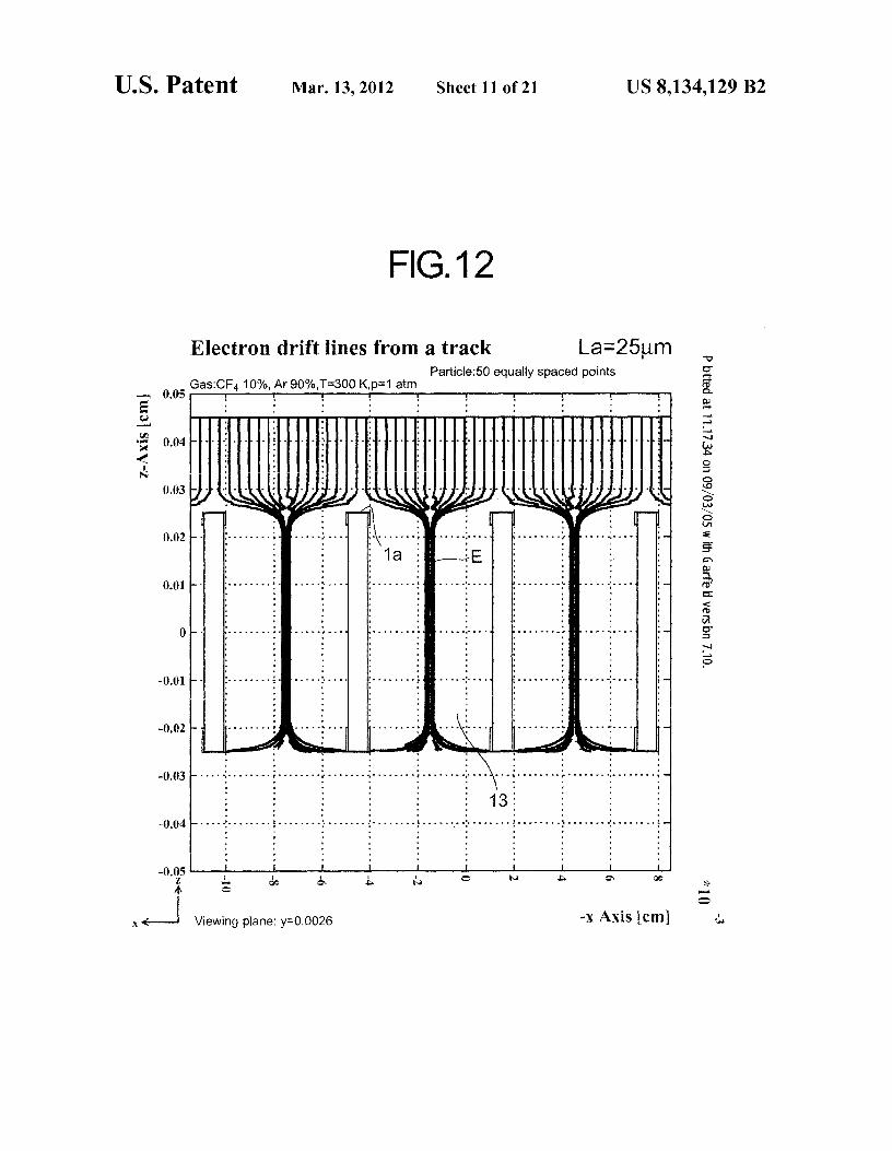
Furthermore, FIGS. 12 to 14 are diagrams showing calcu-lation results of a movement (drift) state of electrons in the channel 13 and in the vicinity of the channel in cases where the lengths La are 25, 50 and 100 µm on a condition that any gas is not present before the electrode la, respectively. It has been confirmed that when the length of the electrode la increases, electrons E present before the electrode la do not easily enter the channel 13.
In addition, FIGS. 15 to 17 are diagrams showing calcula-tionresults of the movement (drift) state ofthe electrons in the channel 13 and in the vicinity of the channel in cases where the lengths La are 25, 50 and 100 µm on the condition that a gas is present before the electrode la, respectively.
Moreover, 1000 virtual electrons were arranged at posi-tions along the extension axis G of the channel 13 with a distance of 400 µm between the electrode la and the front
10 potential point Vt P, and behaviors of the electrons, and a ratio of the electrons which contributed to (participated in) electron multiplication owing to an interaction with a gas in the chan-nel 13 were calculated and evaluated. Results are collectively
5 shown in Table 1.
TABLE 1
Number of electrons (electrons) Ratio (%) of
10 Drift area electrons which
Length La between contributed to elec- of electrode Vr , and Elec- Inner wall of tron multiplica-
la (µm) electrode la trode la channel 13 tion in channel 13
25 18 155 827 16 15 50 23 463 513 14
100 32 946 22 1
From these results, it has been confirmed that when the
20 length of the electrode la increases, the number of the elec-trons which stop in the electrode la increases. In conse-quence, the number of the electrons which reach the inside of the channel 13 decreases, and further the ratio of the electrons which contribute to electron multiplication in the channel 13
25 decreases.Especially, it is understood that when the length La of the electrode la is larger than 50 tm (i.e., La=Lcpx0.1), a ratio at which the electrons E generated in the drift area before the electrode la contribute to the electron multiplication in the channel 13 remarkably decreases. When La is 100 tm
30 (i.e., La=Lcpx0.2) or more, the contribution ratio can be reduced to a substantially negligible ratio.
One of reasons why the electrons E present in the drift area before the electrode la do not easily enter the channel 13 is supposedly that as shown in FIGS. 6 to 8, when the length La
35 of the electrode increases, the portion where the contours are densely spaced changes to a deeper position in the channel 13, whereby the electrons entering an opening end of the channel 13 move so as to enter the electrode la (see FIGS. 12 to 14).
40 However, a function is not limited to this function.
The electron cloud generated in the drift area in this manner does not easily enter the channel 13, and a part of the X-ray Pv which has entered the chamber 22 reaches the MCP 1 without being converted into the electrons owing to the interaction
45 with the gas molecules. When this X-ray Pv enters the elec-trode la, photoelectric conversion is caused by the interaction with the electrode la to generate photoelectrons. At this time, the electrode la includes an alkali metal atom having a reac-tion sectional area of the photoelectric conversion, so that
5o generation efficiency of the photoelectrons is increased. The photoelectrons generated from the electrode la are
generated in the vicinity of the opening of the channel 13 or in the channel 13, and hence immediately enter the channel 13. In the channel 13, an electric field of, for example, 104 V/cm
55 or more is formed so that electric discharge of the gas and excitation emission are sufficiently caused, and the electrons successively collide with the gas molecules to perform the electron multiplication and light multiplication.
In this case, when various reactions are caused and, above 6o all, excited CF4 molecules transit to a base bottom state, light
having a wavelength peculiar to the energy transition is emit-ted (CF4*_CF4+hv). A wavelength region of this excitation emission is broad from visible light to an infrared region (about 400 to 900 mm), and a peak wavelength of the region
65 is about 620 nm. This emission wavelength tends to most match sensitivity of a CCD among specific devices of the photo position detector 3.
US 8,134,129 B2 11
The light which has multiplied in this manner passes through the FOP 2 to enter the photo position detector 3 without being photoelectrically converted again. The photo position detector 3 outputs information on the two-dimen-sional position which the light enters and an electric signal 5
based on light intensity at each incidence position to the control system 35 through the driving circuit board 4, and a three-dimensional X-ray emission image is constituted in the system and output to the display or the like.
Here, FIGS. 20 to 22 are photographs showing results of io imaging. The inner diameter D of the channel 13 was set to 100 µm, the MCP 1 was prepared using Inconel 600 as the electrodes la, 1b, and a test pattern (an aperture) shown in FIG. 19 was disposed before the beryllium window 21 and imaged while irradiated with the X-ray in a high resolution 15
mode to apply a reverse bias voltage. It is to be noted that in the chamber 23, an Ar+CF4 mixture gas having a predeter-mined pressure was introduced. FIGS. 20 to 22 show results in cases where pressures of the mixture gas are 1 atm, 0.5 atm and 0.25 atm, respectively. It is also indicated that when 20
numeric values shown in FIGS. 20 to 22 increase, straight lines reflected adjacent to the values are dense.
It has been confirmed from these results that the MCP 1 of the present invention and the imaging type X-ray detection device 200 using the gas proportional counter provided with 25
the MCP have sufficient imaging sensitivity even in the high resolution mode remarkably excellent in positional resolu-tion. During an operation in a high luminance mode to apply a forward bias, when a gas pressure in the chamber decreases, track lengths of the electrons usually increase. Therefore, 30
when the gas pressure decreases, the resolution tends to dete-riorate. On the other hand, as apparent from FIGS. 20 to 22, it has been found that in the MCP 1 of the present invention and the imaging type X-ray detection device 200 using the gas proportional counter provided with the MCP, even when such 35
a gas pressure in the chamber changes, the deterioration of the resolution is not recognized.
According to the imaging type X-ray detection device 200 using the gas proportional counter provided with the MCP 1 having such a constitution, the electrons highly efficiently 40
generated owing to the interaction between the alkali metal atom included in the electrode la and the X-ray Pv function as an electron source for the electron/light multiplication in the channel 13, so that the imaging with the high luminance (high sensitivity) can be performed. The electron cloud generated 45
in the drift area moves toward the MCP 1 while being diffused in the gas, but the cloud is inhibited from entering the MCP 1. Moreover, the photoelectrons generated in the vicinity of the opening of the channel 13 and in the channel are hardly diffused in the gas, and hence information on the position 50
which the X-ray Pv has entered can more exactly be retained. Then, these photoelectrons function as the electron source for the electron/light multiplication in the channel 13, so that the excellent positional resolution determined by the inner diam-eter of the channel 13 can be realized. Thus, the X-ray imag- 55
ing with the high luminance and the high resolution is real-ized.
It is to be noted that the present invention is not limited to the above-mentioned embodiments, and can variously be modified within the scope of the present invention. For 60
example, a shape of the MCP 1 is not limited to a disc shape, and a square plate-like shape or the like may be used. FIG. 18 is a perspective view schematically showing another example of the MCP according to the present invention. An MCP 10 includes a rectangular outer peripheral frame 212, and a base 65
body 211 provided with a large number of channels 13 and constituted of an insulating member such as glass or a resin is
12 provided on an inner side of the frame. Furthermore, the MCPs 1, 10 do not have to have the outer peripheral frames 12, 212.
Furthermore, a gas of TMA, TEA or the like which pro-duces a penning effect may be added to the gas 217 for detection instead of or in addition to the CF4 gas, but from a viewpoint that the excited light wavelength is in a visible region as described above, an organic gas, for example, alkane halide such as CF4 is more preferable. Furthermore, instead of the FOP 2, a combination of a conventional light transmission window and an optical system may be used, or a bundle-like optical fiber may be used. In addition, the elec-trode lb does not have to include any alkali metal atom.
Moreover, in the above embodiment, the detection and imaging of the X-ray have been described, but a detection target is not limited to the X-ray. The MCP, the gas propor-tional counter and the imaging device according to the present invention may be used in detection of another electromag-netic wave and ionization radiation. Especially, the photo-electric converter portions include the alkali metal atoms, and hence have high sensitivity even with respect to light having a wavelength from an ultraviolet region to a near-infrared region. Even in this case, the above-mentioned example posi-tional resolution can be realized.
Furthermore, the electrode la may be provided with a layer including nuclear species (e.g., 1°B) having a large neutron radiation absorbing sectional area (a sectional area of reaction with respect to neutrons). In this case, the present invention also functions as a detection device of the neutrons. That is, in this case, a nuclear reaction represented by the following formula (3) occurs:
10B+n-4He+7Li+2.78 MeV (3).
At this time, discharged 4He (a-line) and 7Li impart energy to the gas in the channel 13 to generate primary electron cloud, and this primary electron cloud can be a source for the electron/light multiplication in the channel 13. In conse-quence, during the detection of the neutrons. a positional resolution of the order of µm can be achieved. A positional resolution of a usual neutron detector using the gas is of the order of cm. Therefore, according to the MCP, the gas pro-portional counter and the imaging device of the present inven-tion, the positional resolution in the detection of the neutrons can be improved as much as about 1000 times a conventional resolution.
Furthermore, there is not any special restriction on a mate-rial of the porous plate 11. However, when glass is used, the reaction between the alkali metal atom included in the elec-trode la and oxygen can be inhibited. This is preferable from a viewpoint of preventing the deterioration of the electrode la with elapse of time.
INDUSTRIAL APPLICABILITY
As described above, according to a microchannel plate, a gas proportional counter and an imaging device of the present invention, both high luminance and high resolution can be attained at the same time. Therefore, the present invention is broadly usable in any measurement of an electromagnetic wave or ionization radiation, including positional detection.
BRIEF DESCRIPTION OF THE DRAWINGS
FIG. 1 is a plan view schematically showing one preferable embodiment of an MCP according to the present invention;
FIG. 2 is a sectional view cut along the II-II line of FIG. 1;
US 8,134,129 B2 13
FIG. 3 is a main part enlarged view of FIG. 2, and a sectional view schematically showing channels 13 and peripheries of the channels;
FIG. 4 is a perspective view showing one preferable embodiment of an imaging device using a gas proportional counter of the present invention provided with an MCP 1;
FIG. 5 is a sectional view schematically showing a main part of the imaging device shown in FIG. 4;
FIG. 6 is a diagram showing a calculation result of an isoelectric distribution in the vicinity of an opening of a channel 13 in a case where a length La of an electrode la is 25 µm;
FIG. 7 is a diagram showing a calculation result of the isoelectric distribution in the vicinity of the opening of the channel 13 in a case where the length La of the electrode la is 50 µm;
FIG. 8 is a diagram showing a calculation result of the isoelectric distribution in the vicinity of the opening of the channel 13 in a case where the length La of the electrode la is 100 µm;
FIG. 9 is a diagram showing a calculation result of an electric field intensity in the channel 13 in a case where the length La of the electrode la is 25 µm;
FIG. 10 is a diagram showing a calculation result of the electric field intensity in the channel 13 in a case where the length La of the electrode la is 50 µm;
FIG. 11 is a diagram showing a calculation result of the electric field intensity in the channel 13 in a case where the length La of the electrode la is 100 µm;
FIG. 12 is a diagram showing a calculation result of a movement state of electrons in the channel 13 and in the vicinity of the channel in a case where the length La of the electrode la is 25 µm on a condition that any gas is not present before the electrode 1a;
FIG. 13 is a diagram showing a calculation result of the movement state of the electrons in the channel 13 and in the vicinity of the channel in a case where the length La of the electrode la is 50 µm on the condition that any gas is not present before the electrode 1a;
FIG. 14 is a diagram showing a calculation result of the movement state of the electrons in the channel 13 and in the vicinity of the channel in a case where the length La of the electrode la is 100 µm on the condition that any gas is not present before the electrode 1a;
FIG. 15 is a diagram showing a calculation result of the movement state of the electrons in the channel 13 and in the vicinity of the channel in a case where the length La of the electrode la is 25 µm on the condition that a gas is present before the electrode 1a;
FIG. 16 is a diagram showing a calculation result of the movement state of the electrons in the channel 13 and in the vicinity of the channel in a case where the length La of the electrode la is 50 µm on the condition that the gas is present before the electrode 1a;
FIG. 17 is a diagram showing a calculation result of the movement state of the electrons in the channel 13 and in the vicinity of the channel in a case where the length La of the electrode la is 100 µm on the condition that the gas is present before the electrode 1a;
14 FIG. 18 is a perspective view schematically showing
another example of the MCP according to the present inven-tion;
FIG. 19 is a plane photograph showing a test pattern; 5 FIG. 20 is a photograph showing a result obtained by
operating the MCP 1 in a high resolution mode and imaging the test pattern with an X-ray;
FIG. 21 is a photograph showing a result obtained by operating the MCP 1 in the high resolution mode and imaging
10 the test pattern with the X-ray; and FIG. 22 is a photograph showing a result obtained by
operating the MCP 1 in the high resolution mode and imaging the test pattern with the X-ray.
The invention claimed is: 15 1. A microchannel plate which comprises a base body
provided with a plurality of through holes and having an insulating property,
wherein the base body has a first photoelectric converter portion formed on at least inner walls of the plurality of
20 through holes on one end side, and a second photoelec- tric converter portion formed on the inner walls of the plurality of through holes on the other end side and arranged apart from the first photoelectric converter por-tion, and
25 the first and second photoelectric converter portions are configured to also serve as electrodes to apply a prede-termined voltage to opposite ends of the through holes.
2. The microchannel plate according to claim 1, wherein the first and second photoelectric converter por-
30 tions include alkali metal atoms. 3. The microchannel plate according to claim 2, wherein the first and second photoelectric converter por-
tions satisfy a relation represented by the following for-mula (I):
35 Lcpxo.l<La (1),
in which Lcp: a length of each through hole in an axial direction, and La: a length of the first and second photoelectric con-
verter portions along the axial direction of the through 40 hole.
4. The microchannel plate according to claim 1, wherein the first and second photoelectric converter por-
tions include a plurality of types of alkali metal atoms. 5. The microchannel plate according to claim 1,
45 wherein sections of the inner walls of the plurality of through holes have a substantially linear shape which is vertical to a plane direction of the base body.
6. A gas proportional counter which comprises: a chamber filled with a gas for radiation detection mainly
50 including an inert gas and having a window which an electromagnetic wave or ionization radiation enters, and
the MCP arranged in the chamber according to claim 1. 7. The gas proportional counter according to claim 6, wherein the gas for radiation detection contains an organic
55 gas including a halogen atom in molecules. 8. An imaging device which comprises: the gas proportional counter according to claim 6, and a photo-detector arranged after the chamber.