Embed Size (px)
Citation preview

IEICE TRANS. ELECTRON., VOL.E102–C, NO.10 OCTOBER 2019717
PAPER Special Section on Microwave and Millimeter-Wave Technologies
120-W Ku-Band GaN SSPA with Diode Linearizer for FutureBroadcasting Satellites
Masafumi NAGASAKA†a), Masaaki KOJIMA†, Takuma TORII††, Members,Hiromitsu UTSUMI†††, Nonmember, Koji YAMANAKA†††, Shintaro SHINJO††,
Mitsuhiro SHIMOZAWA††, Senior Members, and Hisashi SUJIKAI†, Member
SUMMARY Satellite broadcasting of 4K/8K ultra-high definition tele-vision (UHDTV) was launched in Japan in December 2018. Becausethis system uses the amplitude and phase shift keying (APSK) modula-tion scheme, there is a need to improve the non-linear characteristics ofthe satellite transponders. To meet this requirement, we have been de-veloping a 120-W-class Ku-band solid state power amplifier (SSPA) as areplacement for the currently used traveling wave tube amplifier (TWTA).In this study, we developed a gallium-nitride (GaN) SSPA and linearizer(LNZ). The SSPA achieved an output power of 120 W while maintaining apower added efficiency (PAE) of 31%. We evaluated the transmission per-formance of 16APSK in this SSPA channel in comparison with that in theTWTA channel.key words: broadcasting satellite, SSPA, Ku-band, GaN
1. Introduction
Broadcasting services such as 4K/8K ultra-high defini-tion television (UHDTV) are attracting attention all overthe world [1]. In Japan, the Ministry of Internal Affairsand Communications has issued a road map that calls forUHDTV satellite broadcasting [2]. UHDTV satellite broad-casting services were launched in December 2018.
Ku-band traveling wave tube amplifiers (TWTAs) havebeen used in satellite transponders for providing satellitebroadcasting in Japan, because of their high output power.The TWTA operation requires converting the spacecraft busvoltages into several kilovolts with an electronic power con-ditioner (EPC), and the total weight of the typical Ku-bandTWTA and EPC is 1.8 kg [3]. Therefore, solid state poweramplifiers (SSPAs) have an advantage to mitigate the oper-ating voltage and weight and have been studied as replace-ments for TWTAs in the lower frequency bands [4]. It isalso expected that SSPAs will replace TWTAs operatingin the Ku-Band. As for the signal amplified in the satel-lite, a transmission standard for UHDTV satellite broad-casting (ISDB-S3) has been recommended by ITU-R [5],which deals with modulation schemes of amplitude andphase shift keying (APSK) to increase the transmission ca-
Manuscript received January 31, 2019.Manuscript revised May 24, 2019.†The authors are with NHK Science & Technology Research
Laboratories, Japan Broadcasting Corporation, Tokyo, 157–8510Japan.††The authors are with Mitsubishi Electric Corporation, Infor-
mation Technology R&D Center, Kamakura-shi, 247–8501 Japan.†††The authors are with Mitsubishi Electric Corporation, High
Frequency & Optical Device Works, Itami-shi, 664–8641 Japan.a) E-mail: [email protected]
DOI: 10.1587/transele.2019MMP0006
Fig. 1 Trend in Ku-band PAs.
pacity. TWTAs need to be operated at a large back-off toreduce their non-linearities when APSK signals are trans-mitted.
In general, SSPAs have better linearity thanTWTAs [6]. However, the efficiency and output power ofSSPAs fabricated with gallium-arsenide (GaAs) technologyhave not yet reached the levels of TWTAs. Recently, thechances of obtaining high efficiency and high output powerfrom SSPAs have increased because of the development ofgallium-nitride (GaN) devices. Figure 1 shows the trend ofKu-band power amplifiers (PAs). From 2004 to 2006, 10-W-class devices had been built from GaAs [7]–[9]. In 2009,a GaN PA with an output power of over 50 W under con-tinuous wave (CW) conditions was developed [10]. Since2014, GaN technology has been used to achieve 80-W-classoutput powers [11], [12]. A 120-W-class SSPA applyingthis technology could be a replacement for the 120-W-classTWTA in the current broadcasting satellite transponder [13].So far, we have studied using 100-W-class SSPAs for abroadcasting satellite operating in the 12-GHz band (11.7to 12.2 GHz) [14]–[16].
In this paper, we describe a 120-W-class 12-GHz-bandSSPA. The SSPA comprises a diode linearizer (LNZ), GaNdriver amplifier (DA), and GaN high power amplifier (HPA).The HPA achieves an output power of 120 W (50.8 dBm). Indesigning SSPAs, un-modulated signals are typically usedas the input signal; for example, a LNZ is tuned with atwo-tone signal (two un-modulated-signals). However, wecannot evaluate the transmission performance of APSK sig-nals accurately with these methods. Therefore, we designedand evaluated our SSPA with the 16APSK used for UHDTVsatellite broadcasting in Japan. In Sect. 2, we describe the
Copyright c© 2019 The Institute of Electronics, Information and Communication Engineers

718IEICE TRANS. ELECTRON., VOL.E102–C, NO.10 OCTOBER 2019
satellite transponder model, evaluation methods, and defini-tions for designing the SSPA. Sections 3 and 4 describe thedesign and performance of the SSPA. Section 5 discussesthe transmission performance of 16APSK in SSPA chan-nels. We summarize the paper in Sect. 6.
2. Transmission Model for Broadcasting Satellite
It is important to evaluate the transmission performance overthe whole satellite loopback to develop a 120-W-class SSPAbecause the radio frequency (RF) components of the satel-lite transponder, which includes amplifiers and filters, im-pact digital signals. Below, we describe the satellite channelmodel and the methods used in our evaluation.
2.1 Satellite Channel Model
Figure 2 shows the block diagram of the satellite channelmodel in our simulation, which is mainly made up of a trans-mitter, satellite transponder, and receiver. The dashed linein the figure outlines the configuration of a typical satellitetransponder, which consists of an input multiplexer (IMUX)filter, a TWTA, and an output multiplexer (OMUX) fil-ter [17], [18]. The role of the satellite transponder is to filtera single carrier out of the uplink signals, amplify it, and sendit to the service area.
The specifications of the modulated signal for our eval-uation are listed in Table 1. A 16APSK (FEC code rate:7/9) signal in accordance with ISDB-S3 (Nyquist band-width: 33.7561 MHz, roll-off factor: 0.03) is transmittedfrom the mapper in Fig. 2, because 16APSK is used in4K/8K UHDTV satellite broadcasting in Japan. The “EQ.”block in the receiver means an adaptive equalizer based onthe least-squares-error criterion [19].
Fig. 2 Block diagram of satellite channel model in our simulations.
Table 1 Specifications of modulated signal.
Figure 3 shows the AM/AM and AM/PM characteris-tics of the TWTA, which are actual measurements from in-door tests [17]–[19]. In the case of the 120-W-class TWTA,the normalized output power of 0 dB corresponds to 120 W(50.8 dBm). It is desirable for the TWTA to amplify the sig-nal as much as possible and have maximum output power,because a 45-cm-diameter parabolic reflector antenna isused for reception of the satellite broadcasting [20]. There-fore, the TWTA is operated near the saturation point. Onthe other hand, the transmission performance deteriorates insaturated operation because of the increase in non-linearity.Thus, there is a trade-off between the gain of the amplifierand the linearity.
Figure 4 shows the amplitude and group delay char-acteristics of the IMUX and OMUX filters, which are alsoactual measurements from the indoor tests [17]–[19]. Therole of the IMUX is to filter a single carrier out of the otheradjacent broadcasting waves [21]. The role of the OMUXis to suppress spectrum re-growth induced by operating theTWTA near the saturation point [6]. To play these roles, thenon-uniform group delays within the Nyquist band of theIMUX and OMUX filters remain. These characteristics neg-atively impact transmission performance [22]. Therefore, itis necessary to evaluate the transmission performances ofthe TWTA and SSPA under the same IMUX and OMUXcharacteristics. We used the characteristics of Fig. 4 as com-mon parameters in the simulations of Sects. 3.4 and 4.2 andin the experiments in Sect. 5.
2.2 Definition of OBO
The output back-off (OBO) in the simulations and experi-
Fig. 3 AM/AM and AM/PM characteristics of TWTA.
Fig. 4 Amplitude and group delay characteristics of IMUX and OMUXfilters (central frequency: 12.03436 GHz (BS-17ch) normalized to 0 Hz).
NAGASAKA et al.: 120-W KU-BAND GAN SSPA WITH DIODE LINEARIZER FOR FUTURE BROADCASTING SATELLITES719
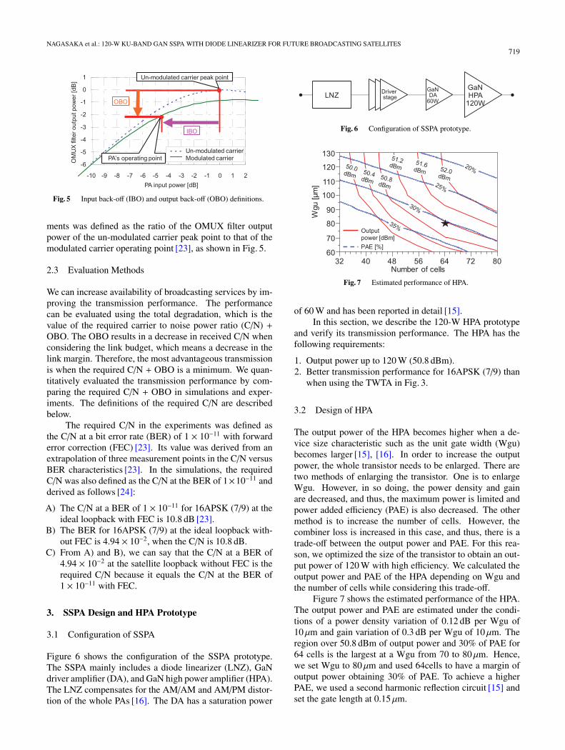
Fig. 5 Input back-off (IBO) and output back-off (OBO) definitions.
ments was defined as the ratio of the OMUX filter outputpower of the un-modulated carrier peak point to that of themodulated carrier operating point [23], as shown in Fig. 5.
2.3 Evaluation Methods
We can increase availability of broadcasting services by im-proving the transmission performance. The performancecan be evaluated using the total degradation, which is thevalue of the required carrier to noise power ratio (C/N) +OBO. The OBO results in a decrease in received C/N whenconsidering the link budget, which means a decrease in thelink margin. Therefore, the most advantageous transmissionis when the required C/N + OBO is a minimum. We quan-titatively evaluated the transmission performance by com-paring the required C/N + OBO in simulations and exper-iments. The definitions of the required C/N are describedbelow.
The required C/N in the experiments was defined asthe C/N at a bit error rate (BER) of 1 × 10⁻¹¹ with forwarderror correction (FEC) [23]. Its value was derived from anextrapolation of three measurement points in the C/N versusBER characteristics [23]. In the simulations, the requiredC/N was also defined as the C/N at the BER of 1×10⁻¹¹ andderived as follows [24]:
A) The C/N at a BER of 1 × 10⁻¹¹ for 16APSK (7/9) at theideal loopback with FEC is 10.8 dB [23].
B) The BER for 16APSK (7/9) at the ideal loopback with-out FEC is 4.94 × 10⁻², when the C/N is 10.8 dB.
C) From A) and B), we can say that the C/N at a BER of4.94 × 10−2 at the satellite loopback without FEC is therequired C/N because it equals the C/N at the BER of1 × 10−11 with FEC.
3. SSPA Design and HPA Prototype
3.1 Configuration of SSPA
Figure 6 shows the configuration of the SSPA prototype.The SSPA mainly includes a diode linearizer (LNZ), GaNdriver amplifier (DA), and GaN high power amplifier (HPA).The LNZ compensates for the AM/AM and AM/PM distor-tion of the whole PAs [16]. The DA has a saturation power
Fig. 6 Configuration of SSPA prototype.
Fig. 7 Estimated performance of HPA.
of 60 W and has been reported in detail [15].In this section, we describe the 120-W HPA prototype
and verify its transmission performance. The HPA has thefollowing requirements:
1. Output power up to 120 W (50.8 dBm).2. Better transmission performance for 16APSK (7/9) than
when using the TWTA in Fig. 3.
3.2 Design of HPA
The output power of the HPA becomes higher when a de-vice size characteristic such as the unit gate width (Wgu)becomes larger [15], [16]. In order to increase the outputpower, the whole transistor needs to be enlarged. There aretwo methods of enlarging the transistor. One is to enlargeWgu. However, in so doing, the power density and gainare decreased, and thus, the maximum power is limited andpower added efficiency (PAE) is also decreased. The othermethod is to increase the number of cells. However, thecombiner loss is increased in this case, and thus, there is atrade-off between the output power and PAE. For this rea-son, we optimized the size of the transistor to obtain an out-put power of 120 W with high efficiency. We calculated theoutput power and PAE of the HPA depending on Wgu andthe number of cells while considering this trade-off.
Figure 7 shows the estimated performance of the HPA.The output power and PAE are estimated under the condi-tions of a power density variation of 0.12 dB per Wgu of10 µm and gain variation of 0.3 dB per Wgu of 10 µm. Theregion over 50.8 dBm of output power and 30% of PAE for64 cells is the largest at a Wgu from 70 to 80 µm. Hence,we set Wgu to 80 µm and used 64cells to have a margin ofoutput power obtaining 30% of PAE. To achieve a higherPAE, we used a second harmonic reflection circuit [15] andset the gate length at 0.15 µm.

720IEICE TRANS. ELECTRON., VOL.E102–C, NO.10 OCTOBER 2019
Fig. 8 Photograph of HPA prototype.
Fig. 9 Measured output performance of HPA (CW frequency: 12.0 GHz,drain bias voltage: 30 V).
Fig. 10 Measured AM/AM and AM/PM characteristics of HPA.
3.3 HPA Prototype
Figure 8 shows the HPA prototype that we fabricated basedon the design in Sect. 3.2, and Fig. 9 shows the measuredoutput performance. The output power resulted in 120 W(50.8 dBm) when the PAE and gain were 31% and 7 dB,respectively. Figure 10 shows the measured AM/AM andAM/PM characteristics for the prototype. Here, the normal-ized input and output powers at the peak point in Fig. 10(both 0 dB) correspond to 43.8 and 50.8 dBm, respectively.Figure 11 shows the recent trend of GaN PAs in the Ku band.To the best of our knowledge, this is the first time that an out-put power of 120 W has been reported for devices operatingin the Ku-band.
Fig. 11 State-of-the-art GaN PAs operating in Ku band.
Table 2 Simulation results of required C/N + OBO for 16APSK (7/9)(TWTA versus HPA systems).
Fig. 12 C/N versus BER characteristics for 16APSK (7/9) without FECat satellite loopback in simulations (total bits: 106): A) IMUX filter –TWTA – OMUX filter [IBO = 4.43 dB, OBO = 2.20 dB], B) IMUX fil-ter – SSPA (HPA) – OMUX filter [IBO = 2.50 dB, OBO = 2.20 dB].
3.4 Simulated Transmission Performance of HPA
To verify requirement B) in Sect. 3.1, we simulated thetransmission performance for 16APSK (7/9) through theHPA prototype. We calculated the required C/N in stepsA) – C) of Sect. 2.3. A block diagram of the simulation isshown in Fig. 2. We compared the TWTA and HPA systemsin terms of the following channel models:
A) IMUX filter (Fig. 4) – TWTA (Fig. 3) – OMUX filter(Fig. 4)
B) IMUX filter – SSPA (HPA) (Fig. 10) – OMUX filter
The OBOs for channels A) and B) were fixed to2.2 dB [13], and the input back-off (IBO) was derived fromthe OBO. Figure 12 shows the C/N versus BER character-istics for 16APSK (7/9) without FEC over channels A) andB). This figure also indicates the values for the ideal loop-

NAGASAKA et al.: 120-W KU-BAND GAN SSPA WITH DIODE LINEARIZER FOR FUTURE BROADCASTING SATELLITES721
back, described in Sect. 2.3. Table 2 lists the total degra-dations in terms of the required C/N + OBOs obtained fromFig. 12. The total degradation for HPA system B) was 0.1 dBsmaller than that for TWTA system A). From these simula-tion results, we confirmed that the transmission performanceof our HPA prototype is equivalent to the TWTA. Thus, inthe next section, we describe the design of a LNZ, whichconnects to the HPA, to improve performance.
4. Linearizer Design and Prototype
We developed a 12-GHz-band LNZ to compensate for dis-tortion due to the amplifier characteristics (AM/AM andAM/PM) of the HPA prototype described in Sect. 3. We didnot consider the LNZ to compensate for the distortion due tothe group delay characteristics in Fig. 4. The required C/N +OBO can be decreased by connecting the LNZ to the HPA,as shown in Fig. 6. The configuration of the LNZ and howits parameters are optimized are described below.
4.1 Design of LNZ
Figure 13 shows the equivalent circuit of the LNZ. We cancompensate for the AM/AM and AM/PM characteristics byusing diodes. However, the AM/PM variation in the 12-GHzband is limited by parasitic inductances between the diodeand ground. To reduce the parasitic inductances, we usedthe topology of a diode linearizer with a virtual ground [25].The input signal is separated into two paths, the phases ofwhich differ by 180 degrees (Fig. 13). Accordingly, a vir-tual short is generated at the center of diode. Therefore, theeffect of the parasitic inductance becomes negligible.
4.2 LNZ Parameter Study with Simulated TransmissionPerformance
The linearity of a PA depends on the shape of the AM/AMand AM/PM characteristics. We compared several charac-teristics corresponding to the LNZ parameters in simula-tions for the LNZ, DA, and HPA connected in series likein Fig. 6. Here, we utilized the characteristics of the DAand HPA as the measurements and assumed that there werefour micro strip line (MSL) lengths in the LNZ for tuning.Figure 14 shows the simulated AM/AM, normalized gain,and AM/PM characteristics of the SSPA (LNZ–DA–HPA)for LNZs with four different MSL lengths.
To select the MSL length (0.5, 1.0, 1.5, or 2.0 mm), weevaluated the transmission performance for 16APSK (7/9)through the LNZs. We calculated the required C/Ns in stepsA) – C) in Sect. 2.3 in the same way as in Sect. 3.4. A blockdiagram of the simulation is shown in Fig. 2. The followingchannel models were compared:
A) IMUX filter (Fig. 4) – SSPA (LNZ (MSL length:0.5 mm) – DA – HPA) (Fig. 14) – OMUX filter (Fig. 4)
B) IMUX filter – SSPA (LNZ (MSL length: 1.0 mm) – DA– HPA) – OMUX filter
Fig. 13 Equivalent circuit of LNZ.
Fig. 14 Simulated AM/AM, normalized gain, and AM/PM characteris-tics of SSPA (LNZs (MSL length: 0.5, 1.0, 1.5, 2.0 mm) – DA – HPA).
Table 3 Simulation results of required C/N + OBOs for 16APSK (7/9)(four different LNZs).
C) IMUX filter – SSPA (LNZ (MSL length: 1.5 mm) – DA– HPA) – OMUX filter
D) IMUX filter – SSPA (LNZ (MSL length: 2.0 mm) – DA– HPA) – OMUX filter
The OBOs from channels A) to D) are 2.2 dB [13]. Table 3lists the total degradations in terms of the required C/N +OBOs in simulations in the same way as in Sect. 3.4. SystemC) (MSL length: 1.5 mm) performed the best because therequired C/N + OBO for it was 14.05 dB. We chose thisMSL length for the LNZ hardware.
4.3 LNZ Prototype
Figure 15 shows a photograph of the 12-GHz-band LNZprototype. The substrate is composed of alumina. Thediodes are implemented on the transmission lines. Figure 16shows the measured AM/AM and AM/PM characteristics ofthe SSPA (LNZ – DA – HPA) which had an LNZ with a 1.5-mm-long MSL. Here, the normalized input (LNZ input) and

722IEICE TRANS. ELECTRON., VOL.E102–C, NO.10 OCTOBER 2019
Fig. 15 Photograph of LNZ prototype.
Fig. 16 Measured AM/AM and AM/PM characteristics of SSPA (LNZ –DA – HPA).
output (HPA output) powers at the peak point in Fig. 16 cor-respond to −5.0 and 50.8 dBm, respectively. We used thisSSPA model in the experiments described in Sect. 5.
5. Transmission Experiments
5.1 Experimental System
Figure 17 shows a block diagram of the transmission systemof our experiments. The dashed line marks the area of the12-GHz-band satellite transponder in the satellite simulatorcomposed of hardware [17]–[19]. We conducted transmis-sion tests by replacing the TWTA with the SSPA inside thissatellite simulator and evaluated the differences in transmis-sion performance in the following channel models:
A) IMUX filter (Fig. 4) – TWTA (Fig. 3) – OMUX filter(Fig. 4)
B) IMUX filter – SSPA (Fig. 16) – OMUX filter
The OBOs of A) and B) were controlled by a variable atten-uator at the IMUX filter output and set to 2.2 dB [13].
The center frequency of the modulated carrier fromthe transmitter was 140 MHz. The satellite simulatorconsisted of a frequency up-converter (from 140 MHzto 12.03436 GHz), 12-GHz-band satellite transponder(satellite channel), and frequency down-converter (from12.03436 GHz to 140 MHz). The modulated signal over thesatellite simulator went into a noise adder for the downlinkC/N measurement.
5.2 Experimental Results
Figure 18 shows the C/N versus BER characteristics for16APSK (7/9). Table 4 lists the required C/N + OBO ob-tained from Fig. 18. The required C/N + OBO for 16APSK
Fig. 17 Block diagram of experimental transmission system.
Fig. 18 C/N versus BER for 16APSK (7/9) with FEC at satellite loop-back in experiments (total bits: 1010): A) IMUX filter – TWTA – OMUXfilter [OBO = 2.2 dB], B) IMUX filter – SSPA – OMUX filter [OBO =2.2 dB].
Table 4 Experimental results of required C/N + OBO for 16APSK (7/9)for TWTA and SSPA systems.
Fig. 19 Received constellations for 16APSK (7/9) at OBO of 2.2 dB.
(7/9) was 14.9 dB at channel A), whereas it was 14.0 dB atchannel B). Under the same OBO of 2.2 dB for both chan-nels, the required C/N +OBO improved by 0.9 dB as a resultof using the developed SSPA.
Figure 19 shows the received constellations withoutdownlink noise for 16APSK (7/9) at channels A) and B).The constellation at B) (SSPA) rotated less than at A)(TWTA). From these constellations, it can be seen that thephase shift of the SSPA, which depends on the input power,is smaller than that of the TWTA.

NAGASAKA et al.: 120-W KU-BAND GAN SSPA WITH DIODE LINEARIZER FOR FUTURE BROADCASTING SATELLITES723
6. Conclusion
We fabricated a 120-W 12-GHz-band SSPA prototype witha diode linearizer for improving 4K/8K satellite broadcast-ing services in the future. We evaluated its transmission per-formance in simulations to determine the design parametersfor the fabrication process and in experiments as a final test.What we obtained from this study are as follows.
• The fabricated HPA achieved a 120-W output powerwith a PAE of 31%. This is the highest output poweryet reported for a single GaN HPA in the 12-GHz band.• We developed a 12-GHz-band LNZ. We designed it
by making an evaluation using the 16APSK signal ofISDB-S3 rather than an un-modulated or two-tone sig-nal. This method is the first such attempt in this field.• We conducted transmission experiments showing that
the transmission performance of 16APSK (7/9) in theSSPA channel improved by 0.9 dB compared with thatin the TWTA channel in operation at an OBO of 2.2 dB.
Acknowledgments
This research was performed under the auspices of a pro-gram called “Research and Development of TechnologyEncouraging Effective Utilization of Frequency for Ultra-high-definition Satellite and Terrestrial Broadcasting Sys-tem” funded by the Ministry of Internal Affairs and Com-munications, Japan.
References
[1] ITU-R, “Parameter values for ultra-high definition television sys-tems for production and international programme exchange,” Rec-ommendation ITU-R BT.2020, Oct. 2015.
[2] The ITU Association of Japan, “Promoting the advancement ofbroadcasting services: the road map to 4K and 8K,” ITU-AJ NewBreeze, vol.26, no.2, Spr. 2014.
[3] L3 Technologies, Electron devices products. Available:https://www2.l3t.com/edd/products/index.htm
[4] K. Osawa, H. Yoshikoshi, A. Nitta, T. Tanaka, E. Mitani, and T.Satoh, “High-Efficiency L-Band 200-W GaN HEMT for Space Ap-plications,” SEI technical review, vol.191, pp.32–37, July 2017 (inJapanese).
[5] ITU-R, “Transmission system for UHDTV satellite broadcasting,”Recommendation ITU-R BO.2098, Dec. 2016.
[6] S. Tirro, “Satellite communication systems design,” New York, theUnited States, Springer, 1993.
[7] Q. Zhang and S.A. Brown, “Fully monolithic 8 watts Ku-band highpower amplifier,” 2004 MTT-S International Microwave SymposiumDigest (IEEE Cat. No.04CH37535), pp.1159–1162, 2004.
[8] C.H. Lin, H.Z. Liu, C.K. Chu, H.K. Huang, Y.H. Wang, C.C. Liu,C.H. Chang, C.L. Wu, and C.S. Chang, “A fully matched Ku-band9W pHEMT MMIC high power amplifier,” Proc. IEEE CompoundSemicond. Integr. Circuits Symp., San Antonio, the United States,pp.165–168, Nov. 2006.
[9] C.-H. Lin, H.-Z. Liu, C.-K. Chu, H.-K. Huang, C.-C. Liu, C.-H.Chang, C.-L. Wu, C.-S. Chang, and Y.-H. Wang, “A compact6.5-W pHEMT MMIC power amplifier for Ku-band applications,”Microwave Wireless Components Lett., vol.17, no.2, pp.154–156,
March 2007.[10] K. Takagi, S. Takatsuka, Y. Kashiwabara, S. Teramoto, K.
Matsushita, H. Sakurai, K. Onodera, H. Kawasaki, Y. Takada, andK. Tsuda, “Ku-band AlGaN/GaN-HEMT with over 30% of PAE,”MTT’09. IEEE MTT-S International Microwave Symposium Di-gest, pp.457–460, June 2009.
[11] S. Imai, H. Maehara, M. Koyanagi, H. Ohtsuka, A. Ohta, K.Yamanaka, A. Inoue, and H. Fukumoto, “An 80-W packaged GaNhigh power amplifier for CW operation in the 13.75–14.5 GHzband,” Proc. 2014 IEEE MTT-S International Microwave Sympo-sium, Tampa, the United States, pp.1–4, June 2014.
[12] T. Torii, S. Imai, H. Maehara, M. Miyashita, T. Kunii, T. Morimoto,A. Inoue, A. Ohta, H. Katayama, N. Yunoue, K, Yamanaka, and H.Fukumoto, “60% PAE, 30W X-band and 33% PAE, 100W Ku-bandPAs utilizing 0.15 µm GaN HEMT technology,” Proc. 46th Euro-pean Microwave Conference (EuMC), London, the United King-dom, pp.568–571, Oct. 2016.
[13] M. Kojima, Y. Suzuki, M. Kamei, Y. Koizumi, S. Saito, S. Tanaka,and H. Nishida, “Transmission experiments for UHDTV using 12GHz band satellite broadcasting,” IEICE Technical Report, vol.115,no.287, SAT2015-49, pp.13–16, Oct. 2015.
[14] M. Kamei, M. Nagasaka, S. Nakazawa, and S. Tanaka, “Design of100-W class GaN power amplifier for on-board SSPA of Ku-bandbroadcasting satellites,” Proc. 33rd AIAA International Communi-cations Satellite Systems Conference, Gold Coast, Australia, AIAA2015-4346, Sept. 2015.
[15] M. Nagasaka, S. Nakazawa, S. Tanaka, T. Torii, S. Imai, H.Utsumi, M. Kono, K. Yamanaka, and H. Fukumoto, “A Ku-band100 W power amplifier under CW operation utilizing 0.15 µm GaNHEMT technology,” Proc. Asia-Pacific Microwave Conference 2016(APMC 2016), New Delhi, India, TH2-A-3, pp.1–4, Dec. 2016.
[16] M. Nagasaka, M. Kojima, S. Nakazawa, H. Sujikai, S. Tanaka, T.Torii, H. Utsumi, S. Shinjo, and M. Shimozawa, “120-W Ku-bandGaN SSPA with diode linearizer for future broadcasting satel-lite,” Proc. Asia-Pacific Microwave Conference 2018 (APMC 2018),Kyoto, Japan, TH2-D-1, pp.548–550, Nov. 2018.
[17] M. Kojima, M. Nagasaka, Y. Koizumi, S. Nakazawa, A. Iwasaki, Y.Suzuki, K. Saito, and S. Tanaka, “APSK transmission experimentsover 12GHz-band satellite channel compared TWTA and SSPA,”Proc. 35th AIAA International Communications Satellite SystemsConference, Trieste, Italy, AIAA 2017-5405, Oct. 2017.
[18] Y. Suzuki, K. Tsuchida, Y. Matsusaki, A. Hashimoto, S. Tanaka, T.Ikeda, and N. Okumura, “Performance evaluation of transmissionsystem for 8K Super Hi-Vision satellite broadcasting,” Proc. IEEEGlobal Communications Conference, Austin, the United States,SAC-18-SVC, pp.2928–2933, Dec. 2014.
[19] M. Kojima, M. Nagasaka, Y. Suzuki, Y. Koizumi, K. Saito, and S.Tanaka, “Experimental verification of prototype equalizer for non-linear compensation over satellite channel,” Transactions of JapanSociety for Aeronautical and Space Sciences Aerospace TechnologyJapan, vol.16, no.3, pp.248–253, May 2018.
[20] ARIB STD-B63 ver. 1.6-E1, “Receiver for Advanced Wide BandDigital Satellite Broadcasting,” Dec. 2016.
[21] M. Kojima, H. Sujikai, Y. Suzuki, A. Hashimoto, S. Tanaka, T.Kimura, and K. Shogen, “A study on influence of interference ofmulti-level digital modulations for broadcasting satellite,” Trans-actions of Japan Society for Aeronautical and Space SciencesAerospace Technology Japan, vol.8, no.ists27, pp.Pj 1–Pj 6, March2011.
[22] E. Casini, R.D. Gaudenzi, and A. Ginesi, “DVB-S2 modem algo-rithms design and performance over typical satellite channels,” In-ternational Journal of Satellite Communications and Networking,vol.22, no.3, pp.281–318, May 2004.
[23] ARIB STD-B44 ver. 2.0-E1, “Transmission system for advancedwide band digital satellite broadcasting,” July 2014.
[24] M. Kojima, Y. Koizumi, Y. Suzuki, and H. Sujikai, “Performancecomparison of digital pre-distortion techniques over satellite chan-

724IEICE TRANS. ELECTRON., VOL.E102–C, NO.10 OCTOBER 2019
nel,” Proc. IEICE Joint Conference on Satellite Communications,Daejeon, Korea, vol.118, no.237, SAT2018-54, pp.67–71, Oct.2018.
[25] H. Noto, K. Yamauchi, and M. Nakayama, “Diode linearizer withvirtual ground for Ku-band power amplifier,” Proc. 2011 IEICEgeneral conference, Tokyo, Japan, C-2-11, p.49, March 2011 (inJapanese).
Masafumi Nagasaka received his B.E.and M.E. degrees in electrical and electronicengineering from Tokyo Institute of Technol-ogy, Tokyo, Japan, in 2001 and 2003. Hejoined Japan Broadcasting Corporation (NHK)in 2003. Since 2008, he has been engaged in re-search on Ku- and Ka-band satellite broadcast-ing systems at NHK Science & Technology Re-search Laboratories. He is currently a seniormanager of the Planning & Coordination Divi-sion of the laboratories. He received the Young
Researcher Award of IEICE in 2011. He is a member of ITE.
Masaaki Kojima received his B.E.,M.E., and Ph.D. degrees in electrical and elec-tronic engineering from Tokushima University,Tokushima, Japan, in 2000, 2002, and 2015. Hejoined Japan Broadcasting Corporation (NHK)in 2002. Since 2006, he has been engagedin research on the non-linear characteristics ofbroadcasting satellite transponders at NHK Sci-ence & Technology Research Laboratories. Heis currently a principal research engineer ofthe laboratories. He received the IEEE CASS
Shikoku Chapter Best Paper Award in 2015 and the JC-SAT Award fromIEICE in 2017. He is an assistant secretary of the Technical Committee onSatellite Telecommunications of IEICE and a member of ITE and IEEE.
Takuma Torii received his B.E. andM.E. degrees from Tokyo University of Science,Tokyo, Japan, in 2012 and 2014. He joinedMitsubishi Electric Corporation in 2014. Since2015, he has been engaged in research on Ku-band power amplifiers at Mitsubishi Electric In-formation Technology R&D Center.
Hiromitsu Utsumi received his B.E. andM.E. degrees in electrical and electronic engi-neering from Waseda University, Tokyo, Japan,in 1994 and 1996. He joined Mitsubishi ElectricCorporation in 1996. Since 1996, he has beenengaged in development of high-frequency de-vices at Mitsubishi Electric Corporation.
Koji Yamanaka received his B.Sc. degreein electric engineering and M.Sc. and Ph.D. de-grees in electronic engineering from the Uni-versity of Tokyo, Japan, in 1993, 1995, and1998, respectively. In 1998, he joined the In-formation Technology Research and Develop-ment Center, Mitsubishi Electric Corporation,Kamakura, Japan, where he engaged in de-velopment of GaAs low-noise monolithic mi-crowave integrated circuit amplifiers and GaNhigh-power amplifiers. From 2012 to 2018, he
managed the Amplifier Group, Mitsubishi Electric Corporation. Currently,he is in charge of the civil application GaN device business section. He isa senior member of IEICE. He was the recipient of the Best Paper Prize ofGAAS2005.
Shintaro Shinjo received his B.S. andM.S. degrees in physics and Ph.D. degreein engineering from Keio University, Tokyo,Japan, in 1996, 1998, and 2011. In 1998,he joined Mitsubishi Electric Corporation,Kamakura, Japan, where he has been involvedin the research and development of monolithicmicrowave integrated circuits and solid-statepower amplifiers. He is currently a group man-ager of the Amplifier Group, Microwave Elec-tronics Technology Department. From 2011 to
2012, he was a visiting scholar at the University of California at San Diego,San Diego, CA, USA. He is a senior member of IEEE. He was a recipientof the Prize for Science and Technology (Development Category) of theCommendation for Science and Technology by the Minister of Education,Culture, Sports, Science and Technology in 2009 and the IEICE ElectronicsSociety Award in 2011.
Mitsuhiro Shimozawa received his B.S.and M.S. degrees in electrical engineering fromthe University of Electro-Communications,Tokyo, Japan, in 1989 and 1991, and thePh.D. degree in electrical engineering fromTokyo Institute of Technology, Tokyo, Japan, in2008. He joined Mitsubishi Electric Corpora-tion, Kanagawa, Japan, in 1991, where he hasbeen engaged in research and development ofmicrowave mixers, converters, and transceivers.He was the recipient of the Electronics Society
Award of IEICE, Japan, in 2011.
Hisashi Sujikai received his B.E. and M.E.degrees in electrical and electronic engineeringfrom Waseda University, Tokyo, Japan, in 1991and 1993. From 2013 to 2017, he was a se-nior manager of the Engineering AdministrationDepartment of Japan Broadcasting Corporation(NHK). Since 2017, he has been engaged in re-search on future satellite broadcasting systemsat NHK Science & Technology Research Lab-oratories. He is currently a senior research en-gineer of the laboratories. He is a vice chair of
the Technical Committee on Satellite Telecommunications of IEICE and amember of ITE.