Embed Size (px)
Citation preview
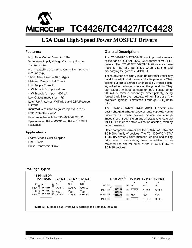
TC4426/TC4427/TC44281.5A Dual High-Speed Power MOSFET Drivers
Features:
• High Peak Output Current – 1.5A
• Wide Input Supply Voltage Operating Range:- 4.5V to 18V
• High Capacitive Load Drive Capability – 1000 pF in 25 ns (typ.)
• Short Delay Times – 40 ns (typ.)
• Matched Rise and Fall Times• Low Supply Current:
- With Logic ‘1’ Input – 4 mA
- With Logic ‘0’ Input – 400 μA• Low Output Impedance – 7Ω• Latch-Up Protected: Will Withstand 0.5A Reverse
Current• Input Will Withstand Negative Inputs Up to 5V
• ESD Protected – 4 kV• Pin-compatible with the TC426/TC427/TC428• Space-saving 8-Pin MSOP and 8-Pin 6x5 DFN
Packages
Applications:
• Switch Mode Power Supplies• Line Drivers
• Pulse Transformer Drive
General Description:
The TC4426/TC4427/TC4428 are improved versionsof the earlier TC426/TC427/TC428 family of MOSFETdrivers. The TC4426/TC4427/TC4428 devices havematched rise and fall times when charging anddischarging the gate of a MOSFET.
These devices are highly latch-up resistant under anyconditions within their power and voltage ratings. Theyare not subject to damage when up to 5V of noise spik-ing (of either polarity) occurs on the ground pin. Theycan accept, without damage or logic upset, up to500 mA of reverse current (of either polarity) beingforced back into their outputs. All terminals are fullyprotected against Electrostatic Discharge (ESD) up to4 kV.
The TC4426/TC4427/TC4428 MOSFET drivers caneasily charge/discharge 1000 pF gate capacitances inunder 30 ns. These devices provide low enoughimpedances in both the on and off states to ensure theMOSFET’s intended state will not be affected, even bylarge transients.
Other compatible drivers are the TC4426A/TC4427A/TC4428A family of devices. The TC4426A/TC4427A/TC4428A devices have matched leading and fallingedge input-to-output delay times, in addition to thematched rise and fall times of the TC4426/TC4427/TC4428 devices.
Package Types
Note 1: Exposed pad of the DFN package is electrically isolated.
8-Pin DFN(1)
NC
IN A
GND
IN B
2
3
4 5
6
7
811
2
3
4
NC
5
6
7
8
OUT A
OUT B
NCIN A
GNDIN B
VDD
TC4426TC4427
TC4426 TC4427
NC
OUT A
OUT BVDD
TC4426TC4427
TC4428
NC
OUT A
OUT BVDD
TC4428 TC4428
NC
OUT A
OUT B
VDD
TC4426 TC4427
NC
OUT A
OUT B
VDD
TC4428
NC
OUT A
OUT B
VDD
8-Pin MSOP/PDIP/SOIC
© 2006 Microchip Technology Inc. DS21422D-page 1
TC4426/TC4427/TC4428
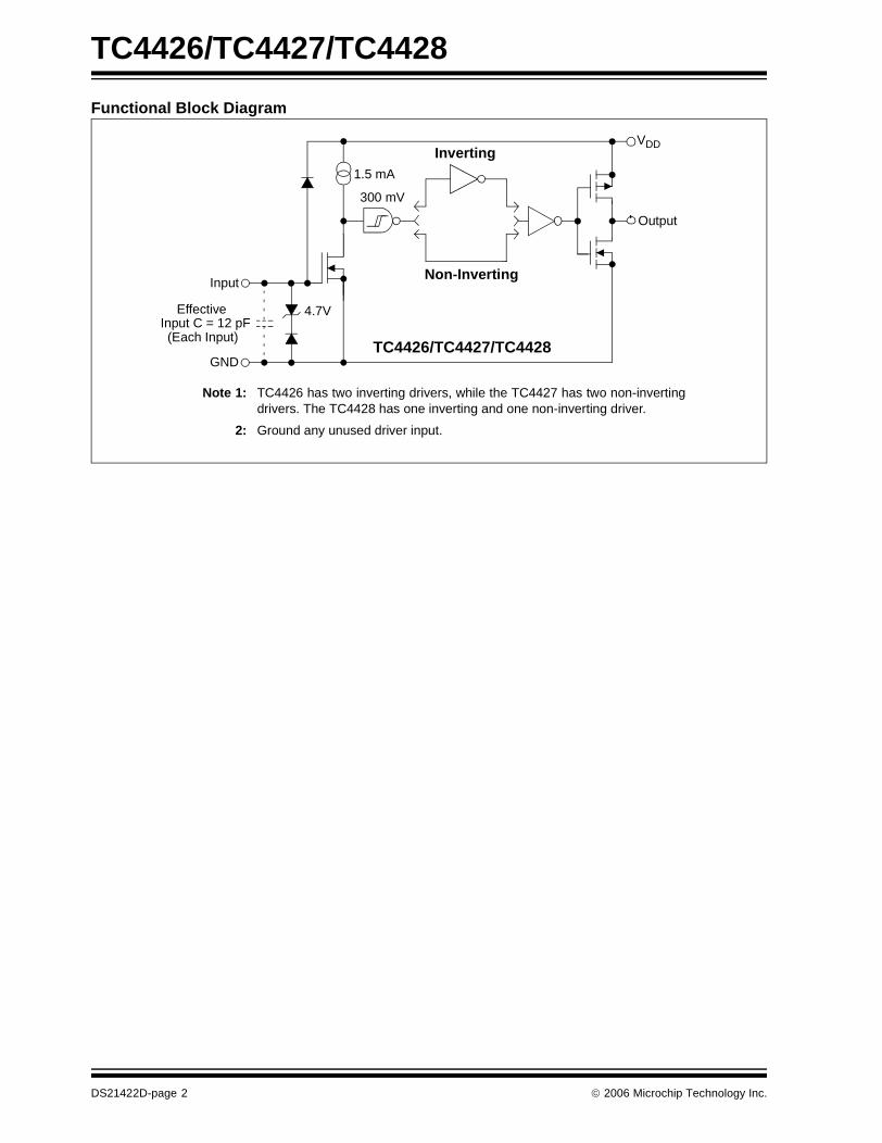
Functional Block Diagram
Effective Input C = 12 pF (Each Input)
TC4426/TC4427/TC4428
Output
Input
GND
VDD
300 mV
4.7V
Inverting
Non-Inverting
Note 1: TC4426 has two inverting drivers, while the TC4427 has two non-invertingdrivers. The TC4428 has one inverting and one non-inverting driver.
2: Ground any unused driver input.
1.5 mA
DS21422D-page 2 © 2006 Microchip Technology Inc.
TC4426/TC4427/TC4428
1.0 ELECTRICAL CHARACTERISTICS
Absolute Maximum Ratings †
Supply Voltage .....................................................+22V
Input Voltage, IN A or IN B..................................... (VDD + 0.3V) to (GND – 5V)
Package Power Dissipation (TA ≤ 70°C)DFN .............................................................. Note 3MSOP..........................................................340 mWPDIP ............................................................ 730 mWSOIC............................................................ 470 mW
Storage Temperature Range.............. -65°C to +150°C
Maximum Junction Temperature...................... +150°C
† Stresses above those listed under “Absolute MaximumRatings” may cause permanent damage to the device. Theseare stress ratings only and functional operation of the deviceat these or any other conditions above those indicated in theoperation sections of the specifications is not implied.Exposure to Absolute Maximum Rating conditions forextended periods may affect device reliability.
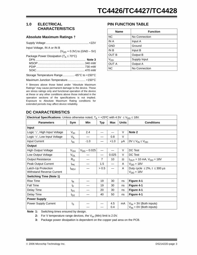
PIN FUNCTION TABLE
DC CHARACTERISTICS
Name Function
NC No Connection
IN A Input A
GND Ground
IN B Input B
OUT B Output B
VDD Supply Input
OUT A Output A
NC No Connection
Electrical Specifications: Unless otherwise noted, TA = +25ºC with 4.5V ≤ VDD ≤ 18V.
Parameters Sym Min Typ Max Units Conditions
Input
Logic ‘1’, High Input Voltage VIH 2.4 — — V Note 2
Logic ‘0’, Low Input Voltage VIL — — 0.8 V
Input Current IIN -1.0 — +1.0 μA 0V ≤ VIN ≤ VDD
Output
High Output Voltage VOH VDD – 0.025 — — V DC Test
Low Output Voltage VOL — — 0.025 V DC Test
Output Resistance RO — 7 10 Ω IOUT = 10 mA, VDD = 18V
Peak Output Current IPK — 1.5 — A VDD = 18V
Latch-Up ProtectionWithstand Reverse Current
IREV — > 0.5 — A Duty cycle ≤ 2%, t ≤ 300 μsVDD = 18V
Switching Time (Note 1)
Rise Time tR — 19 30 ns Figure 4-1
Fall Time tF — 19 30 ns Figure 4-1
Delay Time tD1 — 20 30 ns Figure 4-1
Delay Time tD2 — 40 50 ns Figure 4-1
Power Supply
Power Supply Current IS ——
——
4.50.4
mA VIN = 3V (Both inputs)VIN = 0V (Both inputs)
Note 1: Switching times ensured by design.2: For V temperature range devices, the VIH (Min) limit is 2.0V.
3: Package power dissipation is dependent on the copper pad area on the PCB.
© 2006 Microchip Technology Inc. DS21422D-page 3
TC4426/TC4427/TC4428
DC CHARACTERISTICS (OVER OPERATING TEMPERATURE RANGE)
TEMPERATURE CHARACTERISTICS
Electrical Specifications: Unless otherwise noted, over operating temperature range with 4.5V ≤ VDD ≤ 18V.
Parameters Sym Min Typ Max Units Conditions
Input
Logic ‘1’, High Input Voltage VIH 2.4 — — V Note 2
Logic ‘0’, Low Input Voltage VIL — — 0.8 V
Input Current IIN -10 — +10 μA 0V ≤ VIN ≤ VDD
Output
High Output Voltage VOH VDD – 0.025 — — V DC Test
Low Output Voltage VOL — — 0.025 V DC Test
Output Resistance RO — 9 12 Ω IOUT = 10 mA, VDD = 18V
Peak Output Current IPK — 1.5 — A VDD = 18V
Latch-Up ProtectionWithstand Reverse Current
IREV — >0.5 — A Duty cycle ≤ 2%, t ≤ 300 μsVDD = 18V
Switching Time (Note 1)
Rise Time tR — — 40 ns Figure 4-1
Fall Time tF — — 40 ns Figure 4-1
Delay Time tD1 — — 40 ns Figure 4-1
Delay Time tD2 — — 60 ns Figure 4-1
Power Supply
Power Supply Current IS ——
——
8.00.6
mA VIN = 3V (Both inputs)VIN = 0V (Both inputs)
Note 1: Switching times ensured by design.2: For V temperature range devices, the VIH (Min) limit is 2.0V.
Electrical Specifications: Unless otherwise noted, all parameters apply with 4.5V ≤ VDD ≤ 18V.
Parameters Sym Min Typ Max Units Conditions
Temperature Ranges
Specified Temperature Range (C) TA 0 — +70 °C
Specified Temperature Range (E) TA -40 — +85 °C
Specified Temperature Range (V) TA -40 — +125 °C
Maximum Junction Temperature TJ — — +150 °C
Storage Temperature Range TA -65 — +150 °C
Package Thermal Resistances
Thermal Resistance, 8L-6x5 DFN θJA — 33.2 — °C/W
Thermal Resistance, 8L-MSOP θJA — 206 — °C/W
Thermal Resistance, 8L-PDIP θJA — 125 — °C/W
Thermal Resistance, 8L-SOIC θJA — 155 — °C/W
DS21422D-page 4 © 2006 Microchip Technology Inc.
TC4426/TC4427/TC4428
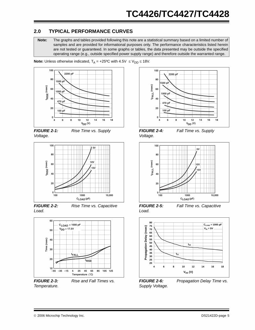
2.0 TYPICAL PERFORMANCE CURVES
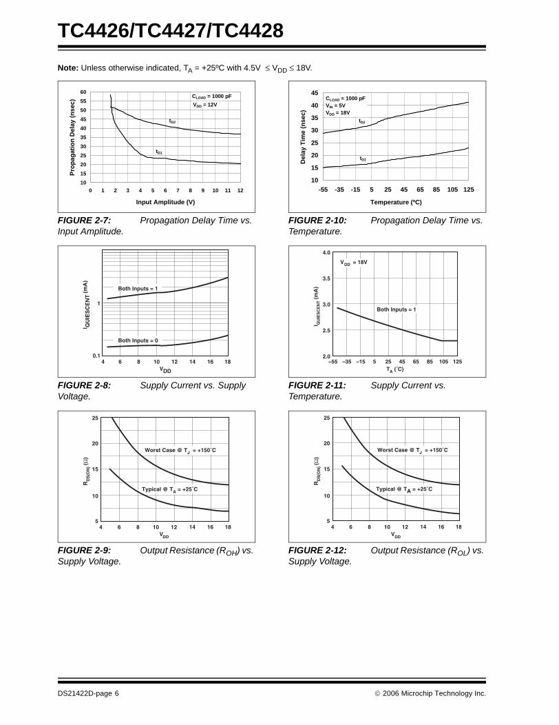
Note: Unless otherwise indicated, TA = +25ºC with 4.5V ≤ VDD ≤ 18V.
FIGURE 2-1: Rise Time vs. Supply Voltage.
FIGURE 2-2: Rise Time vs. Capacitive Load.
FIGURE 2-3: Rise and Fall Times vs. Temperature.
FIGURE 2-4: Fall Time vs. Supply Voltage.
FIGURE 2-5: Fall Time vs. Capacitive Load.
FIGURE 2-6: Propagation Delay Time vs. Supply Voltage.
Note: The graphs and tables provided following this note are a statistical summary based on a limited number ofsamples and are provided for informational purposes only. The performance characteristics listed hereinare not tested or guaranteed. In some graphs or tables, the data presented may be outside the specifiedoperating range (e.g., outside specified power supply range) and therefore outside the warranted range.
t RIS
E (
nse
c)
4 6 8 10 12 14 16 18
100 pF
470 pF
2200 pF
1500 pF
100
1000 pF
80
60
40
20
0
VDD (V)
100 1000 10,000C (pF)LOAD
5V
10V
15V
100
80
60
40
20
0
t RIS
E (
nse
c)T
ime
(nse
c)
tRISE
Temperature (˚C)
C = 1000 pFLOADV = 17.5VDD
60
–55 –35 5 25 45 65 85 105 125–15
tFALL
50
40
30
20
10
t FA
LL
(n
sec)
4 6 8 10 12 14 16 18
100 pF
470 pF
1000 pF
2200 pF
1500 pF
100
80
60
40
20
0
VDD (V)
100 1000 10,000
5V
10V
C (pF)LOAD
100
80
60
40
20
0
t FA
LL
(n
sec)
15V
20253035404550556065707580
4 6 8 10 12 14 16 18
VDD (V)
Pro
pag
atio
n D
elay
(n
sec)
tD1
tD2
CLOAD = 1000 pF
VIN = 5V
© 2006 Microchip Technology Inc. DS21422D-page 5
TC4426/TC4427/TC4428
Note: Unless otherwise indicated, TA = +25ºC with 4.5V ≤ VDD ≤ 18V.
FIGURE 2-7: Propagation Delay Time vs. Input Amplitude.
FIGURE 2-8: Supply Current vs. Supply Voltage.
FIGURE 2-9: Output Resistance (ROH) vs. Supply Voltage.
FIGURE 2-10: Propagation Delay Time vs. Temperature.
FIGURE 2-11: Supply Current vs. Temperature.
FIGURE 2-12: Output Resistance (ROL) vs. Supply Voltage.
10
15
20
25
30
35
40
45
50
55
60
0 1 2 3 4 5 6 7 8 9 10 11 12
Input Amplitude (V)
Pro
pag
atio
n D
elay
(n
sec)
tD1
tD2
CLOAD = 1000 pF
VDD = 12V
4
I
(
mA
)Q
UIE
SC
EN
T
186 8 10 12 14 160.1
Both Inputs = 1
Both Inputs = 0
V DD
1
4 6 8 10 12 14 16 18V DD
RD
S(O
N) (
Ω)
20
25
15
10
5
Worst Case @ TJ = +150˚C
Typical @ TA = +25˚C
10
15
20
25
30
35
40
45
-55 -35 -15 5 25 45 65 85 105 125
Temperature (ºC)
Del
ay T
ime
(nse
c)
tD1
tD2
CLOAD = 1000 pFVIN = 5VVDD = 18V
TA (˚C)
I QU
IES
CE
NT (
mA
)
4.0
3.5
3.0
2.5
2.0–55 –35 –15 5 25 45 65 85 105 125
V = 18VDD
Both Inputs = 1
4 6 8 10 12 14 16 18
20
V DD
25
15
10
5
Worst Case @ TJ = +150˚C
Typical @ TA = +25˚C
RD
S(O
N) (
Ω)
DS21422D-page 6 © 2006 Microchip Technology Inc.
TC4426/TC4427/TC4428
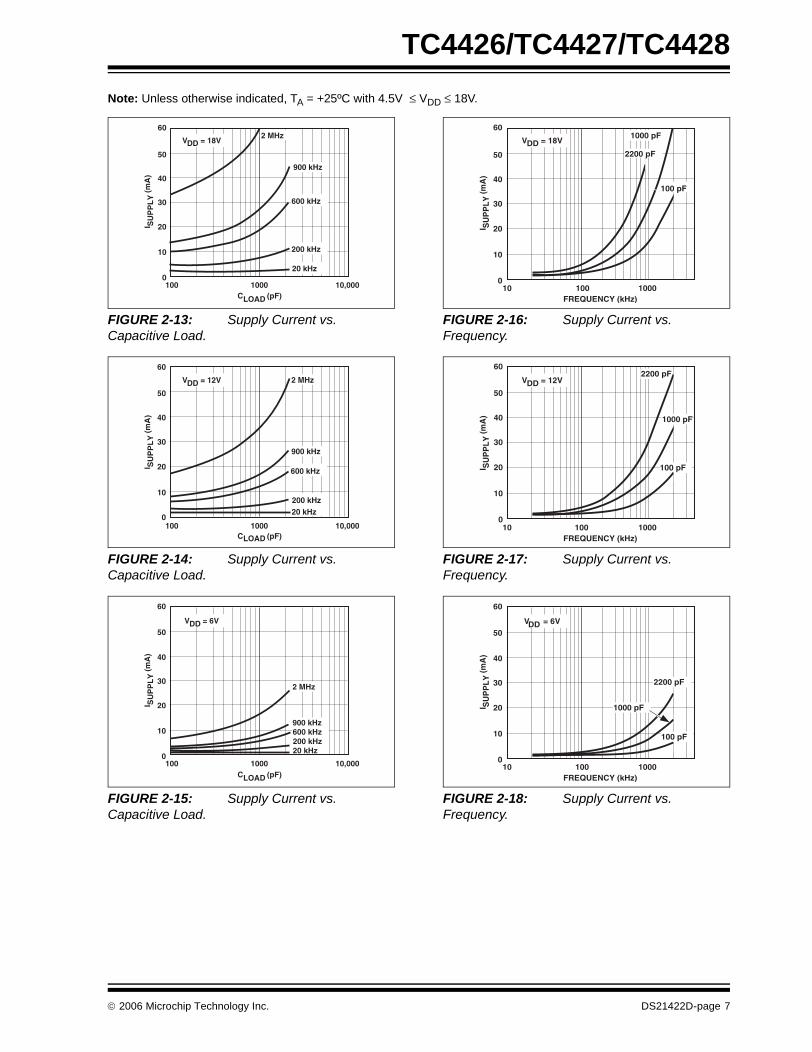
Note: Unless otherwise indicated, TA = +25ºC with 4.5V ≤ VDD ≤ 18V.
FIGURE 2-13: Supply Current vs. Capacitive Load.
FIGURE 2-14: Supply Current vs. Capacitive Load.
FIGURE 2-15: Supply Current vs. Capacitive Load.
FIGURE 2-16: Supply Current vs. Frequency.
FIGURE 2-17: Supply Current vs. Frequency.
FIGURE 2-18: Supply Current vs. Frequency.
60
100 1000 10,000
I SU
PP
LY
(m
A)
2 MHz
600 kHz
200 kHz
20 kHz
900 kHz
C (pF)LOAD
V = 18VDD50
40
30
20
10
0
100 1000 10,000
2 MHz
600 kHz
200 kHz20 kHz
900 kHz
V = 12VDD
C (pF)LOAD
60
50
40
30
20
10
0
I SU
PP
LY
(m
A)
100 1000 10,000
2 MHz
200 kHz20 kHz
600 kHz900 kHz
V = 6VDD
C (pF)LOAD
60
50
40
30
20
10
0
I SU
PP
LY
(m
A)
10 100 1000FREQUENCY (kHz)
1000 pF
2200 pF
V = 18VDD
100 pF
60
50
40
30
20
10
0
I SU
PP
LY (m
A)
10 100 1000FREQUENCY (kHz)
1000 pF
2200 pF
100 pF
V = 12VDD
60
50
40
30
20
10
0
I SU
PP
LY
(m
A)
10 100 1000FREQUENCY (kHz)
1000 pF
2200 pF
100 pF
V = 6VDD
60
50
40
30
20
10
0
I SU
PP
LY (m
A)
© 2006 Microchip Technology Inc. DS21422D-page 7
TC4426/TC4427/TC4428
Note: Unless otherwise indicated, TA = +25ºC with 4.5V ≤ VDD ≤ 18V.
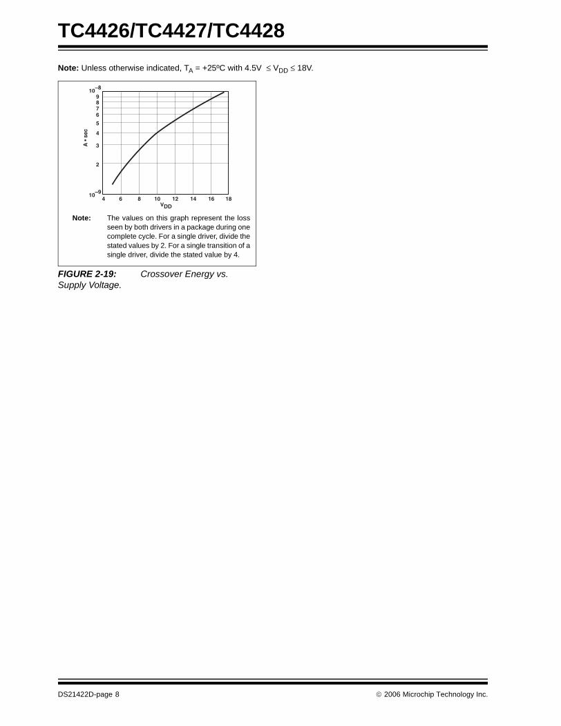
FIGURE 2-19: Crossover Energy vs. Supply Voltage.
4
A •
sec
186 8 10 12 14 16
876
5
4
3
2
10–9
10–8
9
V DD
Note: The values on this graph represent the lossseen by both drivers in a package during onecomplete cycle. For a single driver, divide thestated values by 2. For a single transition of asingle driver, divide the stated value by 4.
DS21422D-page 8 © 2006 Microchip Technology Inc.
TC4426/TC4427/TC4428
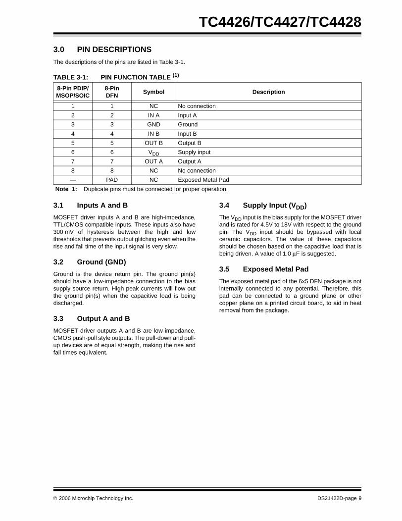
3.0 PIN DESCRIPTIONS
The descriptions of the pins are listed in Table 3-1.
TABLE 3-1: PIN FUNCTION TABLE (1)
3.1 Inputs A and B
MOSFET driver inputs A and B are high-impedance,TTL/CMOS compatible inputs. These inputs also have300 mV of hysteresis between the high and lowthresholds that prevents output glitching even when therise and fall time of the input signal is very slow.
3.2 Ground (GND)
Ground is the device return pin. The ground pin(s)should have a low-impedance connection to the biassupply source return. High peak currents will flow outthe ground pin(s) when the capacitive load is beingdischarged.
3.3 Output A and B
MOSFET driver outputs A and B are low-impedance,CMOS push-pull style outputs. The pull-down and pull-up devices are of equal strength, making the rise andfall times equivalent.
3.4 Supply Input (VDD)
The VDD input is the bias supply for the MOSFET driverand is rated for 4.5V to 18V with respect to the groundpin. The VDD input should be bypassed with localceramic capacitors. The value of these capacitorsshould be chosen based on the capacitive load that isbeing driven. A value of 1.0 μF is suggested.
3.5 Exposed Metal Pad
The exposed metal pad of the 6x5 DFN package is notinternally connected to any potential. Therefore, thispad can be connected to a ground plane or othercopper plane on a printed circuit board, to aid in heatremoval from the package.
8-Pin PDIP/ MSOP/SOIC
8-PinDFN
Symbol Description
1 1 NC No connection
2 2 IN A Input A
3 3 GND Ground
4 4 IN B Input B
5 5 OUT B Output B
6 6 VDD Supply input
7 7 OUT A Output A
8 8 NC No connection
— PAD NC Exposed Metal Pad
Note 1: Duplicate pins must be connected for proper operation.
© 2006 Microchip Technology Inc. DS21422D-page 9
TC4426/TC4427/TC4428
4.0 APPLICATIONS INFORMATION
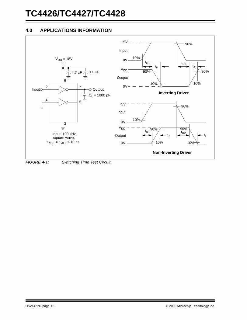
FIGURE 4-1: Switching Time Test Circuit.
CL = 1000 pF
0.1 μF4.7 μF
Inverting Driver
Non-Inverting Driver
Input
VDD = 18V
Input
Output
tD1tF
tR
tD2Input: 100 kHz,square wave,
tRISE = tFALL ≤ 10 ns
Output
Input
Output
tD1tF
tR
tD2
+5V
10%
90%
10%
90%
10%
90%VDD
0V
90%
10%
10% 10%
90%
+5V
VDD
0V
0V
0V
90%
3
2 7
6
4 5
DS21422D-page 10 © 2006 Microchip Technology Inc.
TC4426/TC4427/TC4428
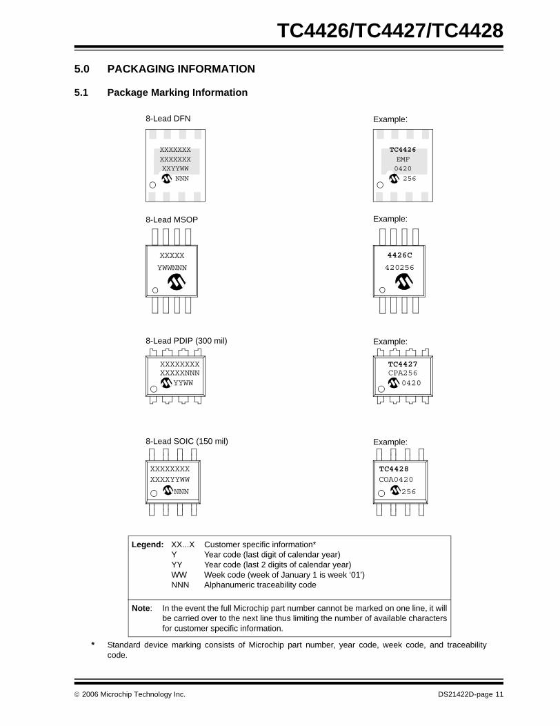
5.0 PACKAGING INFORMATION
5.1 Package Marking Information
XXXXXXXXXXXXXNNN
YYWW
8-Lead PDIP (300 mil) Example:
TC4427CPA256
0420
8-Lead SOIC (150 mil) Example:
XXXXXXXXXXXXYYWW
NNN
TC4428COA0420
256
8-Lead MSOP Example:
XXXXX
YWWNNN
4426C
420256
Legend: XX...X Customer specific information*Y Year code (last digit of calendar year)YY Year code (last 2 digits of calendar year)WW Week code (week of January 1 is week ‘01’)NNN Alphanumeric traceability code
Note: In the event the full Microchip part number cannot be marked on one line, it willbe carried over to the next line thus limiting the number of available charactersfor customer specific information.
* Standard device marking consists of Microchip part number, year code, week code, and traceabilitycode.
8-Lead DFN Example:
XXXXXXX
XXXXXXXXXYYWW
NNN
TC4426
EMF0420
256
© 2006 Microchip Technology Inc. DS21422D-page 11
TC4426/TC4427/TC4428
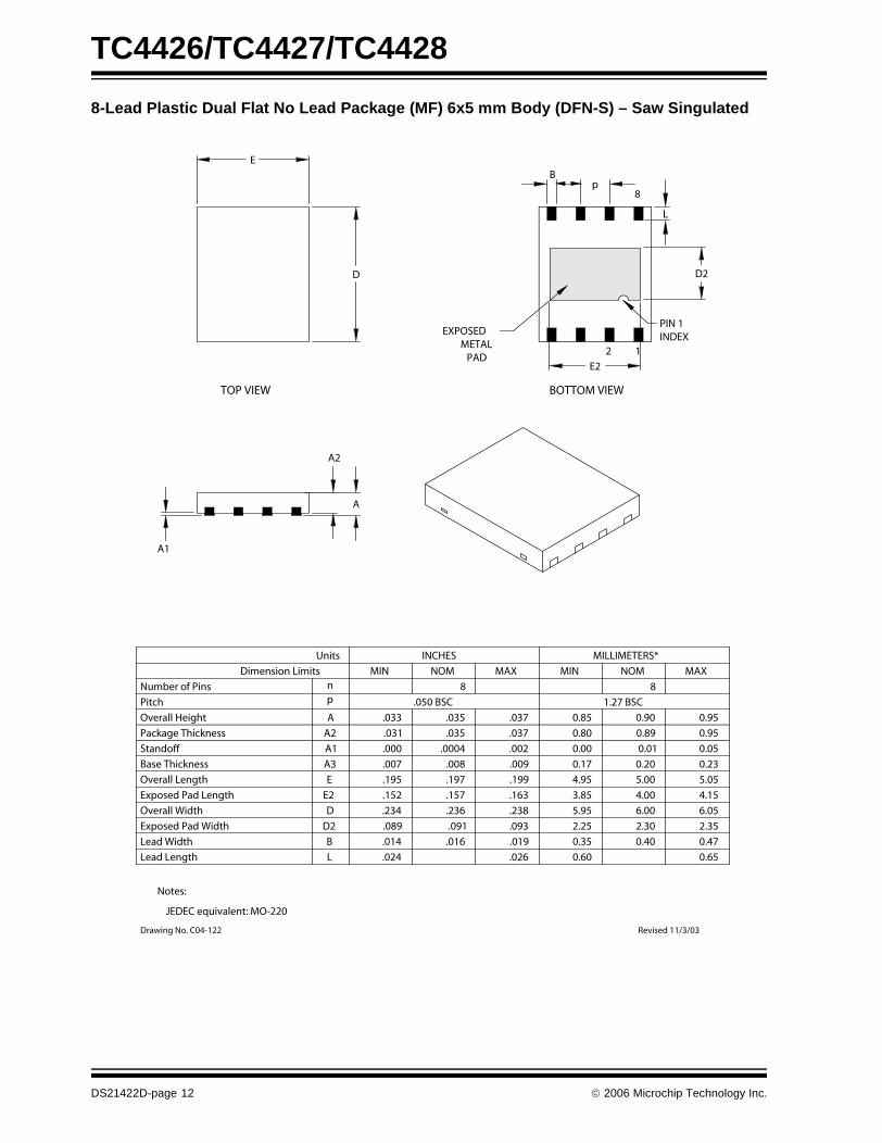
8-Lead Plastic Dual Flat No Lead Package (MF) 6x5 mm Body (DFN-S) – Saw Singulated
DS21422D-page 12 © 2006 Microchip Technology Inc.
TC4426/TC4427/TC4428
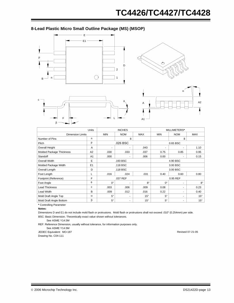
8-Lead Plastic Micro Small Outline Package (MS) (MSOP)
D
A
A1L
c
α
A2
E1
E
p
B n 1
2
φ
β
F
Dimensions D and E1 do not include mold flash or protrusions. Mold flash or protrusions shall not exceed .010" (0.254mm) per side.
.037 REFFFootprint (Reference)
Notes:
Revised 07-21-05
* Controlling Parameter
Mold Draft Angle Top
Mold Draft Angle Bottom
Foot Angle
Lead Width
Lead Thickness
β
α
c
B
φ
.003
.009
.006
.012
Dimension Limits
Overall Height
Molded Package Thickness
Molded Package Width
Overall Length
Foot Length
Standoff
Overall Width
Number of Pins
Pitch
A
L
E1
D
A1
E
A2
.016 .024
.118 BSC
.118 BSC
.000
.030
.193 BSC
.033
MIN
p
n
Units
.026 BSC
NOM
8
INCHES
0.95 REF
-
-
.009
.016
0.08
0.22
0°
0.23
0.40
8°
MILLIMETERS*
0.65 BSC
0.85
3.00 BSC
3.00 BSC
0.60
4.90 BSC
.043
.031
.037
.006
0.40
0.00
0.75
MINMAX NOM
1.10
0.80
0.15
0.95
MAX
8
- -
-
15°5° -
15°5° -
JEDEC Equivalent: MO-187
0° - 8°
5°
5° -
-
15°
15°
--
- -
BSC: Basic Dimension. Theoretically exact value shown without tolerances.
REF: Reference Dimension, usually without tolerance, for information purposes only.
See ASME Y14.5M
See ASME Y14.5M
Drawing No. C04-111
© 2006 Microchip Technology Inc. DS21422D-page 13
TC4426/TC4427/TC4428
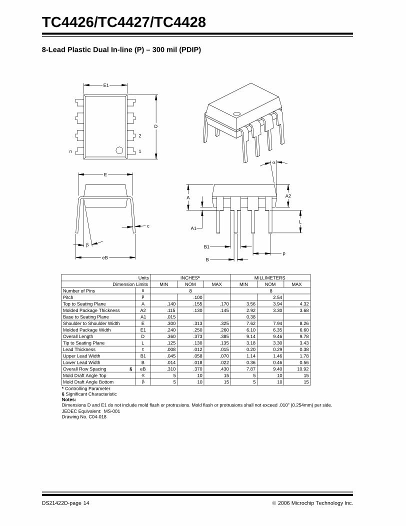
8-Lead Plastic Dual In-line (P) – 300 mil (PDIP)
B1
B
A1
A
L
A2
p
α
E
eB
β
c
E1
n
D
1
2
Units INCHES* MILLIMETERSDimension Limits MIN NOM MAX MIN NOM MAX
Number of Pins n 8 8Pitch p .100 2.54Top to Seating Plane A .140 .155 .170 3.56 3.94 4.32Molded Package Thickness A2 .115 .130 .145 2.92 3.30 3.68Base to Seating Plane A1 .015 0.38Shoulder to Shoulder Width E .300 .313 .325 7.62 7.94 8.26Molded Package Width E1 .240 .250 .260 6.10 6.35 6.60Overall Length D .360 .373 .385 9.14 9.46 9.78Tip to Seating Plane L .125 .130 .135 3.18 3.30 3.43Lead Thickness c .008 .012 .015 0.20 0.29 0.38Upper Lead Width B1 .045 .058 .070 1.14 1.46 1.78Lower Lead Width B .014 .018 .022 0.36 0.46 0.56Overall Row Spacing § eB .310 .370 .430 7.87 9.40 10.92Mold Draft Angle Top α 5 10 15 5 10 15Mold Draft Angle Bottom β 5 10 15 5 10 15* Controlling Parameter
Notes:Dimensions D and E1 do not include mold flash or protrusions. Mold flash or protrusions shall not exceed .010” (0.254mm) per side. JEDEC Equivalent: MS-001Drawing No. C04-018
§ Significant Characteristic
DS21422D-page 14 © 2006 Microchip Technology Inc.
TC4426/TC4427/TC4428
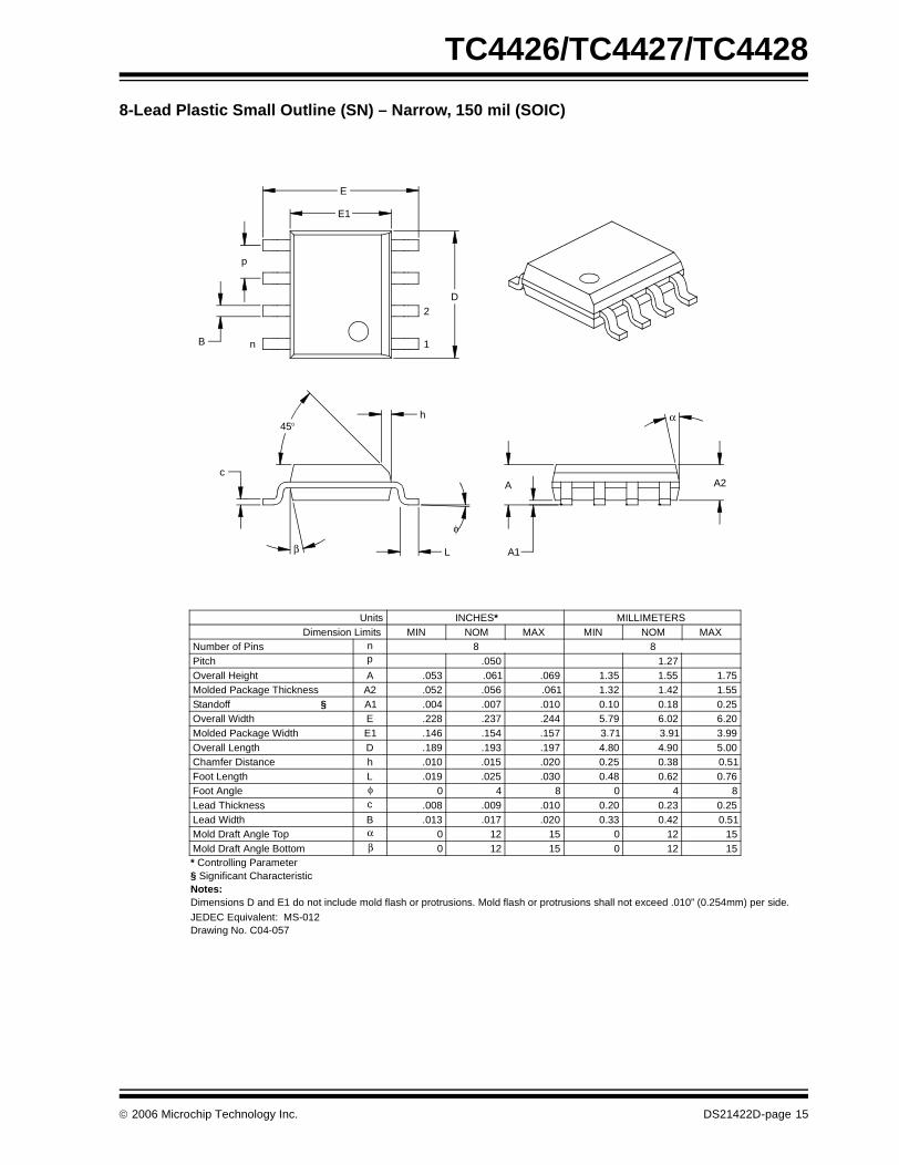
8-Lead Plastic Small Outline (SN) – Narrow, 150 mil (SOIC)
Foot Angle φ 0 4 8 0 4 8
1512015120βMold Draft Angle Bottom1512015120αMold Draft Angle Top
0.510.420.33.020.017.013BLead Width0.250.230.20.010.009.008cLead Thickness
0.760.620.48.030.025.019LFoot Length0.510.380.25.020.015.010hChamfer Distance5.004.904.80.197.193.189DOverall Length3.993.913.71.157.154.146E1Molded Package Width6.206.025.79.244.237.228EOverall Width0.250.180.10.010.007.004A1Standoff §1.551.421.32.061.056.052A2Molded Package Thickness1.751.551.35.069.061.053AOverall Height
1.27.050pPitch88nNumber of Pins
MAXNOMMINMAXNOMMINDimension LimitsMILLIMETERSINCHES*Units
2
1
D
n
p
B
E
E1
h
Lβ
c
45°
φ
A2
α
A
A1
* Controlling Parameter
Notes:Dimensions D and E1 do not include mold flash or protrusions. Mold flash or protrusions shall not exceed .010” (0.254mm) per side.
JEDEC Equivalent: MS-012Drawing No. C04-057
§ Significant Characteristic
© 2006 Microchip Technology Inc. DS21422D-page 15
TC4426/TC4427/TC4428
NOTES:
DS21422D-page 16 © 2006 Microchip Technology Inc.
TC4426/TC4427/TC4428
PRODUCT IDENTIFICATION SYSTEM
To order or obtain information, e.g., on pricing or delivery, refer to the factory or the listed sales office.
Sales and Support
Device: TC4426: 1.5A Dual MOSFET Driver, InvertingTC4427: 1.5A Dual MOSFET Driver, Non-InvertingTC4428: 1.5A Dual MOSFET Driver, Complementary
Temperature Range: C = 0°C to +70°C (PDIP and SOIC only)E = -40°C to +85°CV = -40°C to +125°C
Package: MF = Dual, Flat, No-Lead (6X5 mm Body), 8-leadMF713 = Dual, Flat, No-Lead (6X5 mm Body), 8-lead
(Tape and Reel)OA = Plastic SOIC, (150 mil Body), 8-leadOA713 = Plastic SOIC, (150 mil Body), 8-lead
(Tape and Reel)PA = Plastic DIP (300 mil Body), 8-leadUA = Plastic Micro Small Outline (MSOP), 8-leadUA713 = Plastic Micro Small Outline (MSOP), 8-lead
(Tape and Reel)
Examples:
a) TC4426COA: 1.5A Dual InvertingMOSFET driver,0°C to +70°CSOIC package.
b) TC4426EUA: 1.5A Dual InvertingMOSFET driver,-40°C to +85°C.MSOP package.
c) TC4426EMF: 1.5A Dual InvertingMOSFET driver,-40°C to +85°C,DFN package.
a) TC4427CPA: 1.5A Dual Non-InvertingMOSFET driver,0°C to +70°CPDIP package.
b) TC4427EPA: 1.5A Dual Non-InvertingMOSFET driver,-40°C to +85°CPDIP package.
a) TC4428COA713:1.5A Dual ComplementaryMOSFET driver,0°C to +70°C,SOIC package,Tape and Reel.
b) TC4428EMF: 1.5A Dual Complementary,MOSFET driver,-40°C to +85°CDFN package.
PART NO. X XX
PackageTemperatureRange
Device
XXX
Tape & Reel
X
PB Free
Data SheetsProducts supported by a preliminary Data Sheet may have an errata sheet describing minor operational differences and recommended workarounds. To determine if an errata sheet exists for a particular device, please contact one of the following:
1. Your local Microchip sales office2. The Microchip Corporate Literature Center U.S. FAX: (480) 792-72773. The Microchip Worldwide Site (www.microchip.com)
Please specify which device, revision of silicon and Data Sheet (include Literature #) you are using.
Customer Notification SystemRegister on our web site (www.microchip.com/cn) to receive the most current information on our products.
© 2006 Microchip Technology Inc. DS21422D-page 17

TC4426/TC4427/TC4428
NOTES:
DS21422D-page 18 © 2006 Microchip Technology Inc.
Note the following details of the code protection feature on Microchip devices:
• Microchip products meet the specification contained in their particular Microchip Data Sheet.
• Microchip believes that its family of products is one of the most secure families of its kind on the market today, when used in the intended manner and under normal conditions.
• There are dishonest and possibly illegal methods used to breach the code protection feature. All of these methods, to our knowledge, require using the Microchip products in a manner outside the operating specifications contained in Microchip’s Data Sheets. Most likely, the person doing so is engaged in theft of intellectual property.
• Microchip is willing to work with the customer who is concerned about the integrity of their code.
• Neither Microchip nor any other semiconductor manufacturer can guarantee the security of their code. Code protection does not mean that we are guaranteeing the product as “unbreakable.”
Code protection is constantly evolving. We at Microchip are committed to continuously improving the code protection features of ourproducts. Attempts to break Microchip’s code protection feature may be a violation of the Digital Millennium Copyright Act. If such actsallow unauthorized access to your software or other copyrighted work, you may have a right to sue for relief under that Act.
Information contained in this publication regarding deviceapplications and the like is provided only for your convenienceand may be superseded by updates. It is your responsibility toensure that your application meets with your specifications.MICROCHIP MAKES NO REPRESENTATIONS OR WAR-RANTIES OF ANY KIND WHETHER EXPRESS OR IMPLIED,WRITTEN OR ORAL, STATUTORY OR OTHERWISE,RELATED TO THE INFORMATION, INCLUDING BUT NOTLIMITED TO ITS CONDITION, QUALITY, PERFORMANCE,MERCHANTABILITY OR FITNESS FOR PURPOSE.Microchip disclaims all liability arising from this information andits use. Use of Microchip’s products as critical components inlife support systems is not authorized except with expresswritten approval by Microchip. No licenses are conveyed,implicitly or otherwise, under any Microchip intellectual propertyrights.
© 2006 Microchip Technology Inc.
Trademarks
The Microchip name and logo, the Microchip logo, Accuron, dsPIC, KEELOQ, microID, MPLAB, PIC, PICmicro, PICSTART, PRO MATE, PowerSmart, rfPIC, and SmartShunt are registered trademarks of Microchip Technology Incorporated in the U.S.A. and other countries.
AmpLab, FilterLab, Migratable Memory, MXDEV, MXLAB, PICMASTER, SEEVAL, SmartSensor and The Embedded Control Solutions Company are registered trademarks of Microchip Technology Incorporated in the U.S.A.
Analog-for-the-Digital Age, Application Maestro, dsPICDEM, dsPICDEM.net, dsPICworks, ECAN, ECONOMONITOR, FanSense, FlexROM, fuzzyLAB, In-Circuit Serial Programming, ICSP, ICEPIC, Linear Active Thermistor, MPASM, MPLIB, MPLINK, MPSIM, PICkit, PICDEM, PICDEM.net, PICLAB, PICtail, PowerCal, PowerInfo, PowerMate, PowerTool, Real ICE, rfLAB, rfPICDEM, Select Mode, Smart Serial, SmartTel, Total Endurance, UNI/O, WiperLock and Zena are trademarks of Microchip Technology Incorporated in the U.S.A. and other countries.
SQTP is a service mark of Microchip Technology Incorporated in the U.S.A.
All other trademarks mentioned herein are property of their respective companies.
© 2006, Microchip Technology Incorporated, Printed in the U.S.A., All Rights Reserved.
Printed on recycled paper.
DS21422D-page 19
Microchip received ISO/TS-16949:2002 quality system certification for its worldwide headquarters, design and wafer fabrication facilities in Chandler and Tempe, Arizona and Mountain View, California in October 2003. The Company’s quality system processes and procedures are for its PICmicro® 8-bit MCUs, KEELOQ® code hopping devices, Serial EEPROMs, microperipherals, nonvolatile memory and analog products. In addition, Microchip’s quality system for the design and manufacture of development systems is ISO 9001:2000 certified.
DS21422D-page 20 © 2006 Microchip Technology Inc.
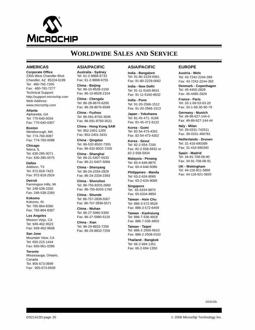
AMERICASCorporate Office2355 West Chandler Blvd.Chandler, AZ 85224-6199Tel: 480-792-7200 Fax: 480-792-7277Technical Support: http://support.microchip.comWeb Address: www.microchip.com
AtlantaAlpharetta, GA Tel: 770-640-0034 Fax: 770-640-0307
BostonWestborough, MA Tel: 774-760-0087 Fax: 774-760-0088
ChicagoItasca, IL Tel: 630-285-0071 Fax: 630-285-0075
DallasAddison, TX Tel: 972-818-7423 Fax: 972-818-2924
DetroitFarmington Hills, MI Tel: 248-538-2250Fax: 248-538-2260
KokomoKokomo, IN Tel: 765-864-8360Fax: 765-864-8387
Los AngelesMission Viejo, CA Tel: 949-462-9523 Fax: 949-462-9608
San JoseMountain View, CA Tel: 650-215-1444Fax: 650-961-0286
TorontoMississauga, Ontario, CanadaTel: 905-673-0699 Fax: 905-673-6509
ASIA/PACIFICAustralia - SydneyTel: 61-2-9868-6733 Fax: 61-2-9868-6755
China - BeijingTel: 86-10-8528-2100 Fax: 86-10-8528-2104
China - ChengduTel: 86-28-8676-6200 Fax: 86-28-8676-6599
China - FuzhouTel: 86-591-8750-3506 Fax: 86-591-8750-3521
China - Hong Kong SARTel: 852-2401-1200 Fax: 852-2401-3431
China - QingdaoTel: 86-532-8502-7355Fax: 86-532-8502-7205
China - ShanghaiTel: 86-21-5407-5533 Fax: 86-21-5407-5066
China - ShenyangTel: 86-24-2334-2829Fax: 86-24-2334-2393
China - ShenzhenTel: 86-755-8203-2660 Fax: 86-755-8203-1760
China - ShundeTel: 86-757-2839-5507 Fax: 86-757-2839-5571
China - WuhanTel: 86-27-5980-5300Fax: 86-27-5980-5118
China - XianTel: 86-29-8833-7250Fax: 86-29-8833-7256
ASIA/PACIFICIndia - BangaloreTel: 91-80-2229-0061 Fax: 91-80-2229-0062
India - New DelhiTel: 91-11-5160-8631Fax: 91-11-5160-8632
India - PuneTel: 91-20-2566-1512Fax: 91-20-2566-1513
Japan - YokohamaTel: 81-45-471- 6166 Fax: 81-45-471-6122
Korea - GumiTel: 82-54-473-4301Fax: 82-54-473-4302
Korea - SeoulTel: 82-2-554-7200Fax: 82-2-558-5932 or 82-2-558-5934
Malaysia - PenangTel: 60-4-646-8870Fax: 60-4-646-5086
Philippines - ManilaTel: 63-2-634-9065Fax: 63-2-634-9069
SingaporeTel: 65-6334-8870Fax: 65-6334-8850
Taiwan - Hsin ChuTel: 886-3-572-9526Fax: 886-3-572-6459
Taiwan - KaohsiungTel: 886-7-536-4818Fax: 886-7-536-4803
Taiwan - TaipeiTel: 886-2-2500-6610 Fax: 886-2-2508-0102
Thailand - BangkokTel: 66-2-694-1351Fax: 66-2-694-1350
EUROPEAustria - WelsTel: 43-7242-2244-399Fax: 43-7242-2244-393Denmark - CopenhagenTel: 45-4450-2828 Fax: 45-4485-2829
France - ParisTel: 33-1-69-53-63-20 Fax: 33-1-69-30-90-79
Germany - MunichTel: 49-89-627-144-0 Fax: 49-89-627-144-44
Italy - Milan Tel: 39-0331-742611 Fax: 39-0331-466781
Netherlands - DrunenTel: 31-416-690399 Fax: 31-416-690340
Spain - MadridTel: 34-91-708-08-90Fax: 34-91-708-08-91
UK - WokinghamTel: 44-118-921-5869Fax: 44-118-921-5820
WORLDWIDE SALES AND SERVICE
10/31/05