Embed Size (px)
Citation preview
1/84
浙江大学研究生课程—纳米技术与系统
AFM 及扫描成像的若干关键问题研究
浙江大学 信息学部 光电信息工程学系浙江大学 信息学部 光电信息工程学系 2015-04-132015-04-13
章海军
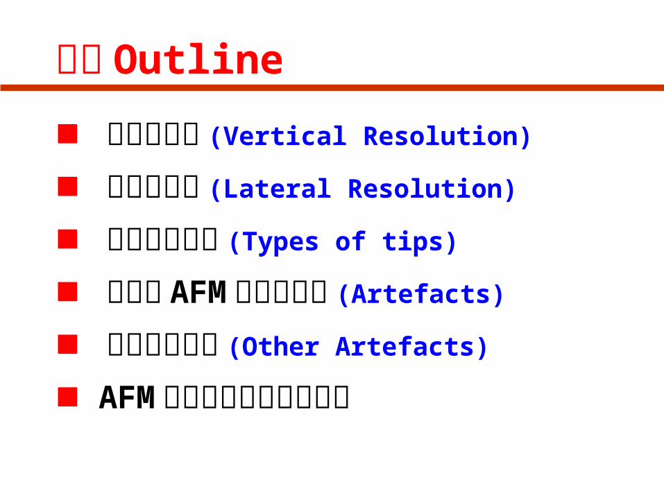
提纲 Outline
纵向分辨率 (Vertical Resolution)
横向分辨率 (Lateral Resolution)
探针不同形式 (Types of tips)
探针对 AFM 图像的影响 (Artefacts)
其他因素影响 (Other Artefacts)
AFM 图像畸变与失真及校正
3/84
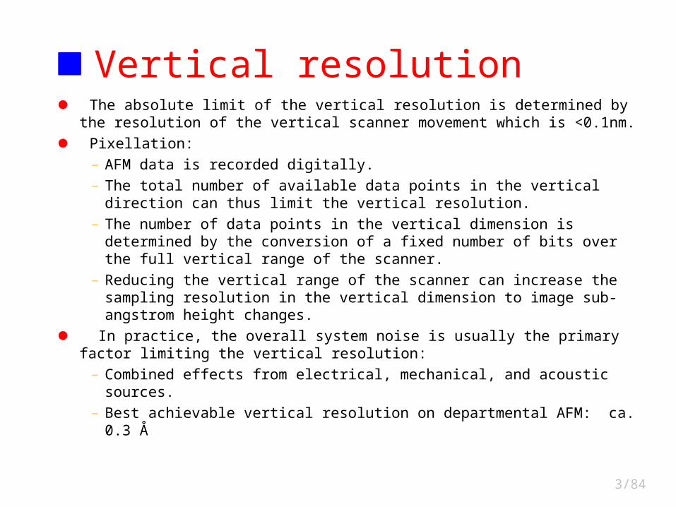
Vertical resolution The absolute limit of the vertical resolution is determined by the resolution
of the vertical scanner movement which is <0.1nm.
Pixellation:
– AFM data is recorded digitally.
– The total number of available data points in the vertical direction can thus limit the vertical resolution.
– The number of data points in the vertical dimension is determined by the conversion of a fixed number of bits over the full vertical range of the scanner.
– Reducing the vertical range of the scanner can increase the sampling resolution in the vertical dimension to image sub-angstrom height changes.
In practice, the overall system noise is usually the primary factor limiting the vertical resolution:
– Combined effects from electrical, mechanical, and acoustic sources.
– Best achievable vertical resolution on departmental AFM: ca. 0.3 Å
4/84
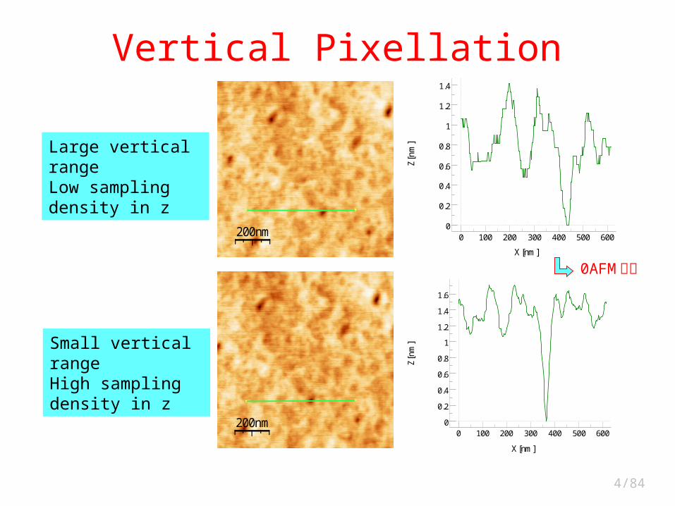
Vertical Pixellation
200nm
200nm 6005004003002001000
1.4
1.2
1
0.8
0.6
0.4
0.2
0
X[nm]
Z[n
m]
6005004003002001000
1.6
1.4
1.2
1
0.8
0.6
0.4
0.2
0
X[nm]
Z[n
m]
Large vertical rangeLow sampling density in z
Small vertical rangeHigh sampling density in z
0AFM截面
5/84
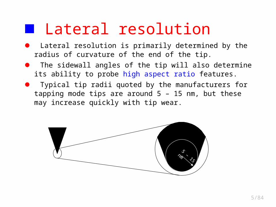
Lateral resolution is primarily determined by the radius of curvature of the end of the tip.
The sidewall angles of the tip will also determine its ability to probe high aspect ratio features.
Typical tip radii quoted by the manufacturers for tapping mode tips are around 5 – 15 nm, but these may increase quickly with tip wear.
Lateral resolution
5 – 15 nm
6/84
Lateral resolution and pixellation The number of lines in an AFM scan, and the number of
samples per line may be set in most AFM software.
Regardless of the pixel size, the feedback loop is sampling
the topography many times at each pixel.
The data displayed at each pixel is the average of the
sampling iterations by the feedback loop over the pixel area.
Obviously, features smaller than the pixel size will not be
properly resolved.
Increasing the sampling density gives improved resolution but
results in slower scanning.
7/84
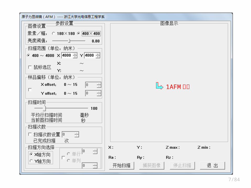
1AFM软件
8/84
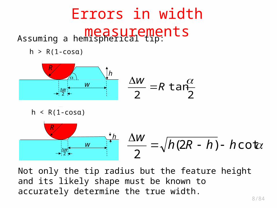
Errors in width measurementsAssuming a hemispherical tip:
cot)2(2
hhRhw
2tan
2
R
w
Not only the tip radius but the feature height and its likely shape must be known to accurately determine the true width.
ww2
h
h > R(1-cosα)
R
h < R(1-cosα)
w2
hR
w
9/84
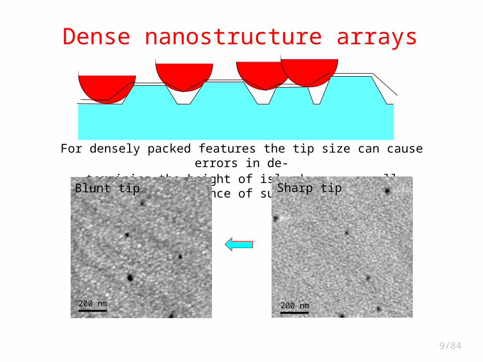
For densely packed features the tip size can cause errors in de-termining the height of islands, or overall appearance of surface
Dense nanostructure arrays
Blunt tip
200 nm
Sharp tip
200 nm
10/84
11/84
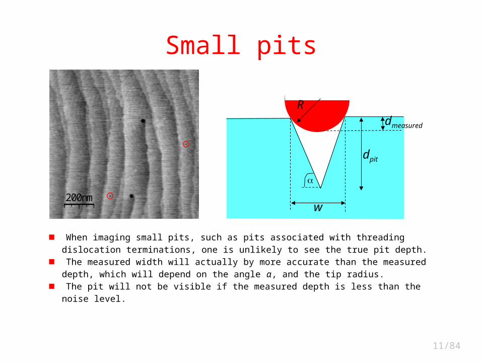
Small pits
When imaging small pits, such as pits associated with threading dislocation terminations, one is unlikely to see the true pit depth.
The measured width will actually by more accurate than the measured depth, which will depend on the angle α, and the tip radius.
The pit will not be visible if the measured depth is less than the noise level.
R
w
dpit
dmeasured
200nm
12/84
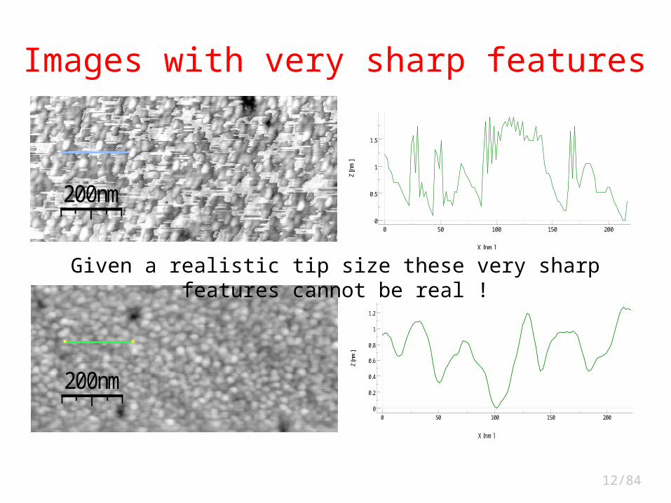
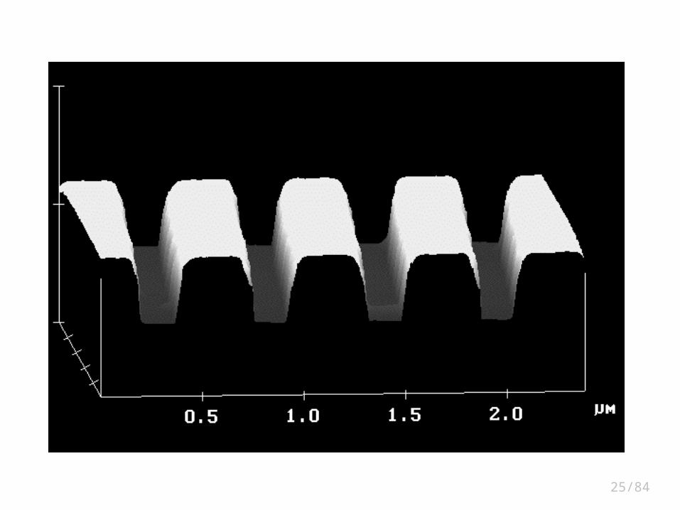
Images with very sharp features
200nm
200nm200nm
200nm200150100500
1.2
1
0.8
0.6
0.4
0.2
0
X[nm]
Z[n
m]
200150100500
1.5
1
0.5
0
X[nm]
Z[n
m]
Given a realistic tip size these very sharp features cannot be real !
13/84
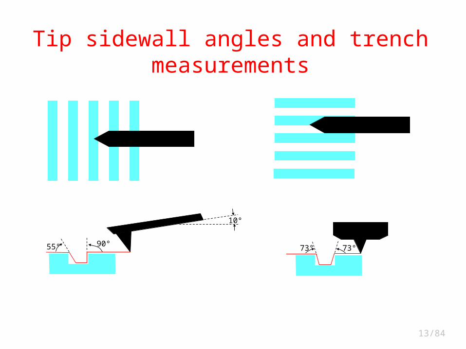
Tip sidewall angles and trench measurements
10°
55° 90°73° 73°
14/84
Types of Specialist tips
for AFMs
15/84
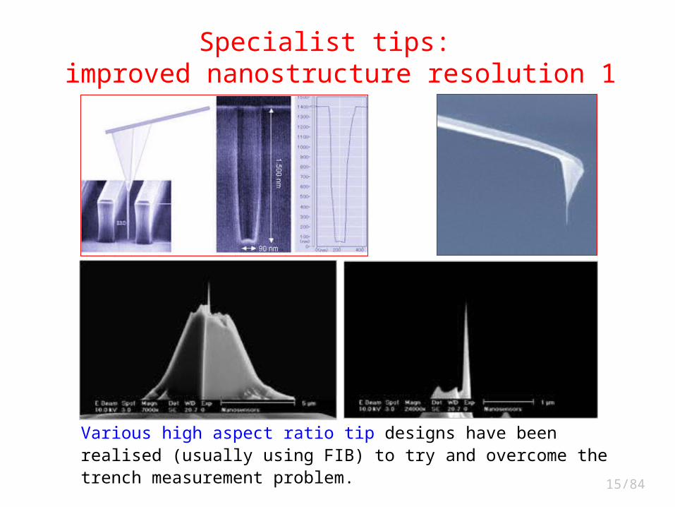
Various high aspect ratio tip designs have been realised (usually using FIB) to try and overcome the trench measurement problem.
Specialist tips: improved nanostructure resolution 1
16/84
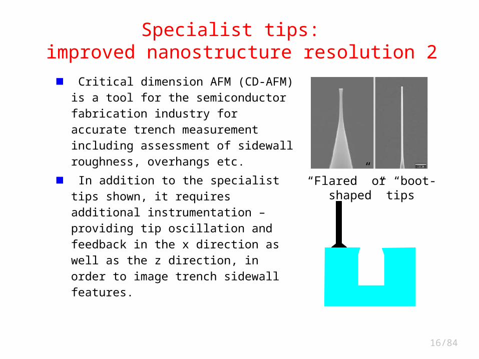
Critical dimension AFM (CD-AFM) is a tool for the semiconductor fabrication industry for accurate trench measurement including assessment of sidewall roughness, overhangs etc.
In addition to the specialist tips shown, it requires additional instrumentation – providing tip oscillation and feedback in the x direction as well as the z direction, in order to image trench sidewall features.
“Flared” or “boot-shaped” tips
Specialist tips: improved nanostructure resolution 2
17/84
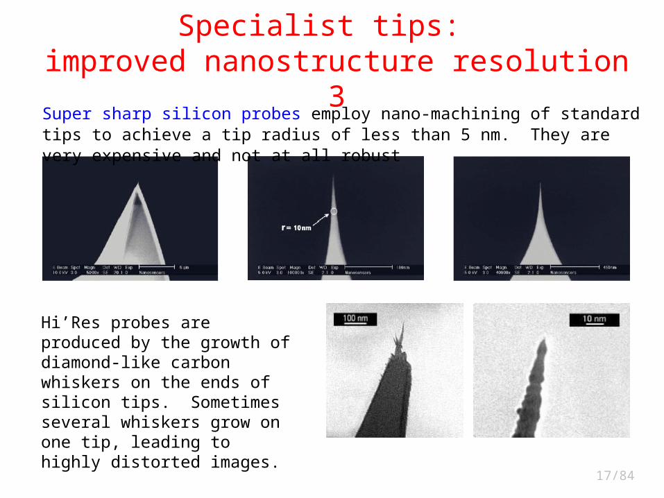
Specialist tips: improved nanostructure resolution 3
Super sharp silicon probes employ nano-machining of standard tips to achieve a tip radius of less than 5 nm. They are very expensive and not at all robust
Hi’Res probes are produced by the growth of diamond-like carbon whiskers on the ends of silicon tips. Sometimes several whiskers grow on one tip, leading to highly distorted images.
18/84
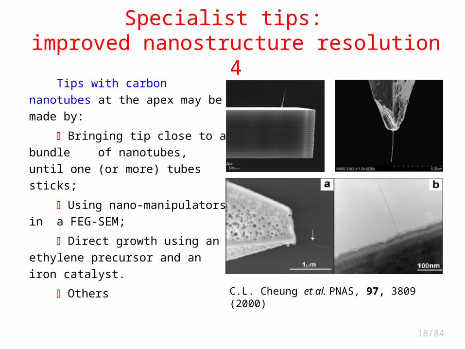
Tips with carbon nanotubes at
the apex may be made by:
Bringing tip close to a bundle
of nanotubes, until one (or more)
tubes sticks;
Using nano-manipulators in a
FEG-SEM;
Direct growth using an
ethylene precursor and an iron
catalyst.
OthersC.L. Cheung et al. PNAS, 97, 3809 (2000)
Specialist tips: improved nanostructure resolution 4
19/84
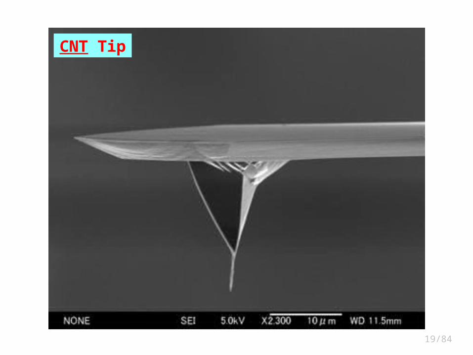
CNT Tip
20/84
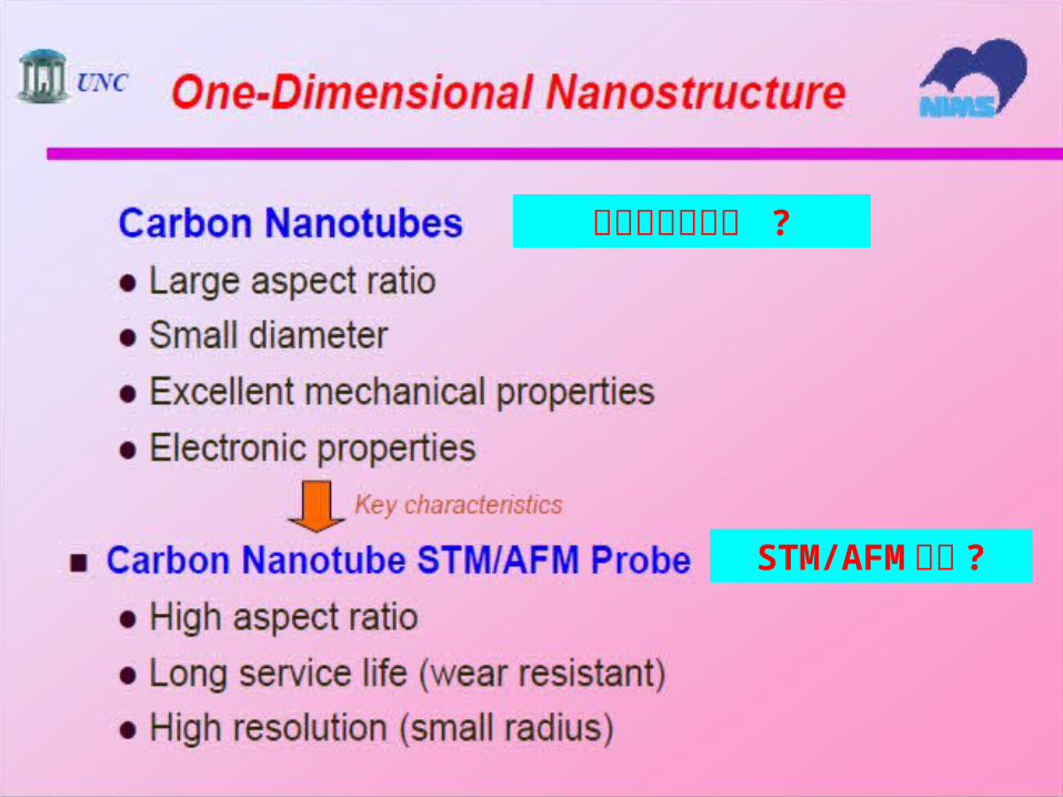
碳纳米管的特点 ?
STM/AFM 探针 ?
21/84
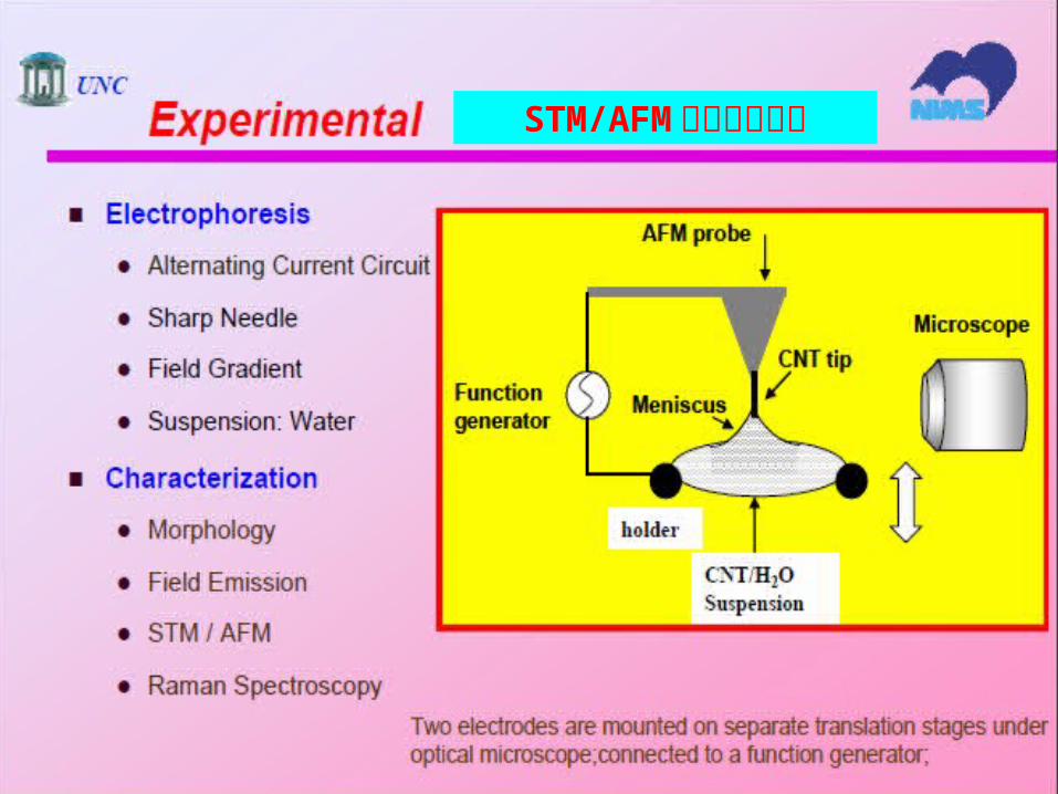
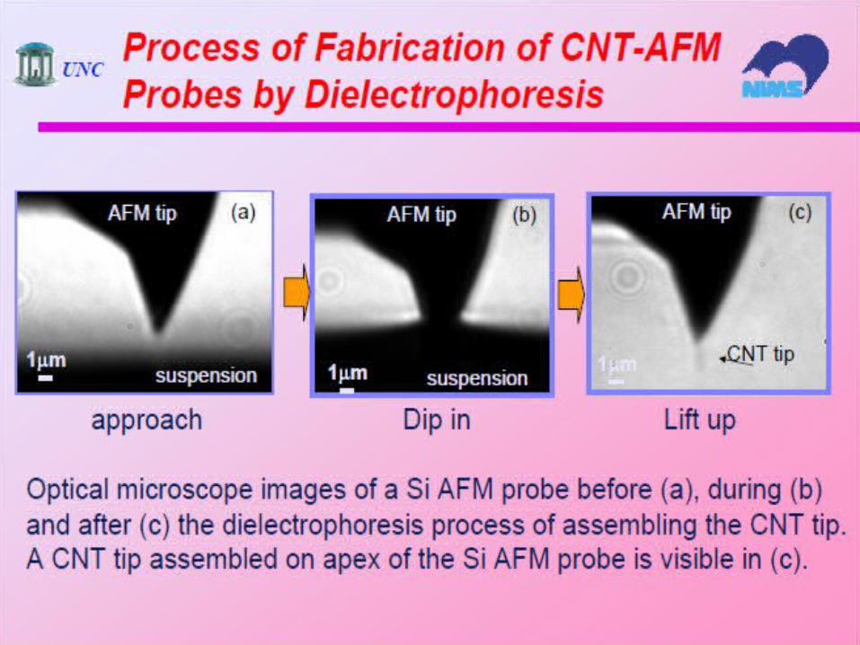
STM/AFM 探针制备方法
22/84
23/84
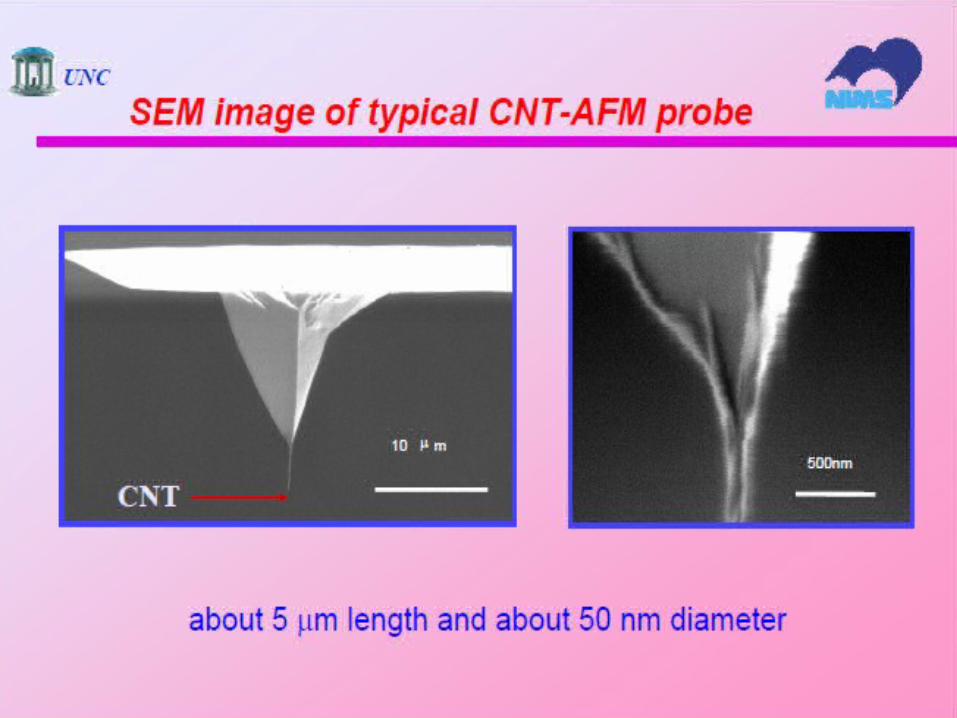
24/84
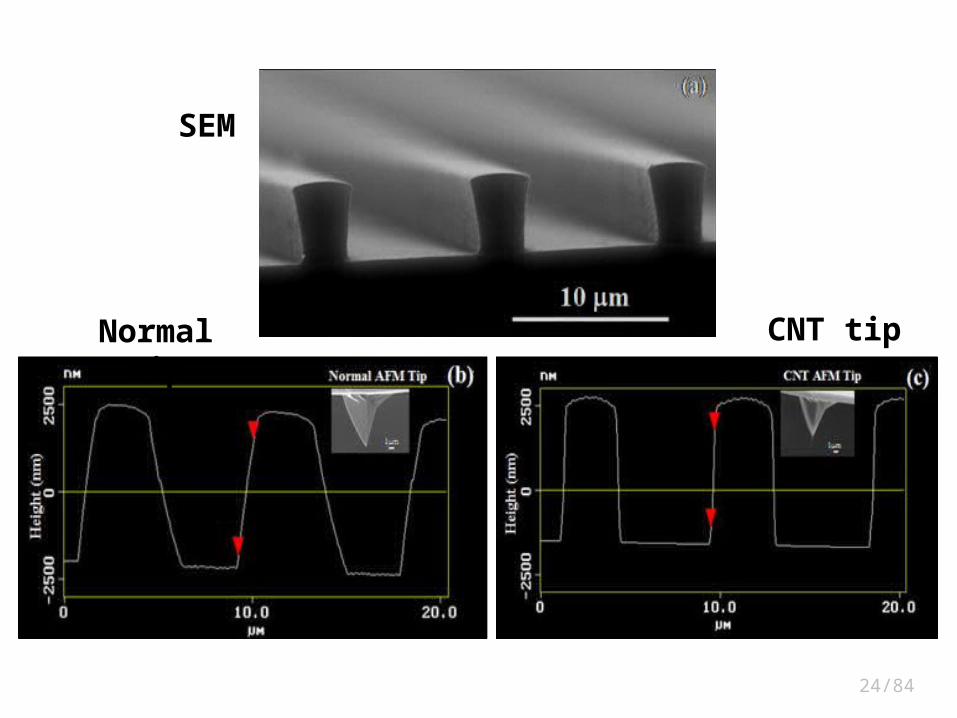
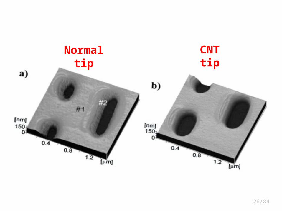
SEM
Normal tip CNT tip
25/84
26/84
Normal tip CNT tip
27/84
Artefacts of AFM tips
28/84
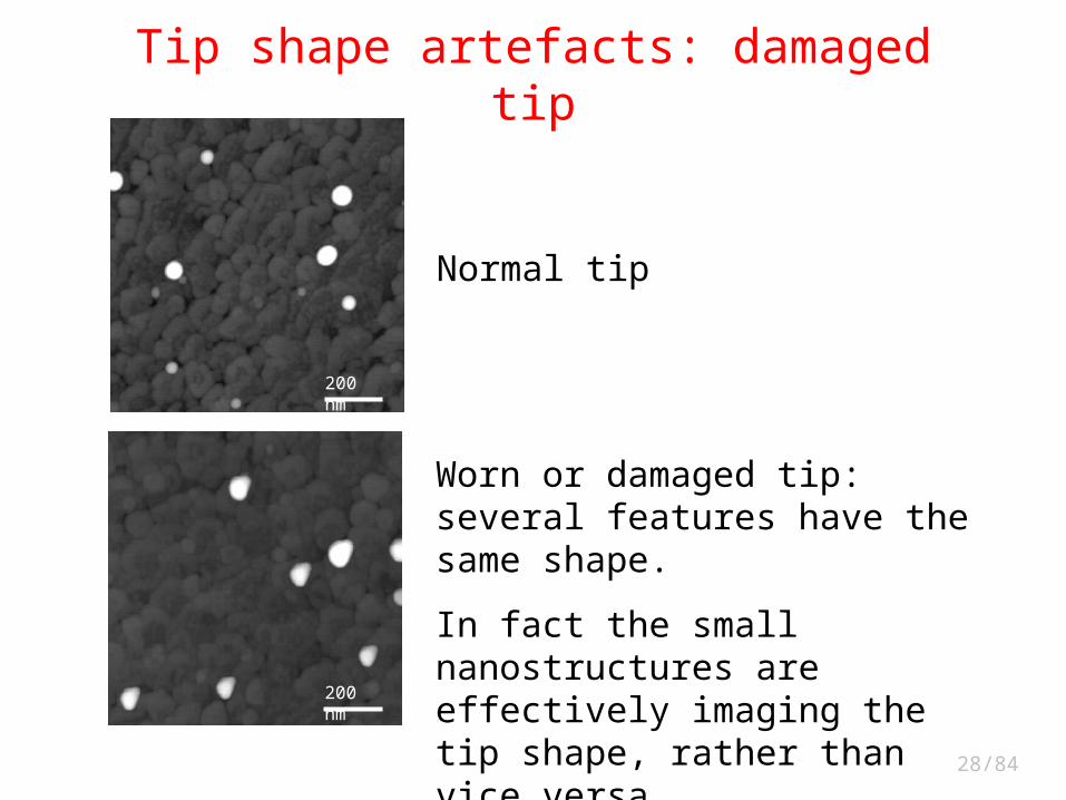
Tip shape artefacts: damaged tip
Normal tip
Worn or damaged tip: several features have the same shape.
In fact the small nanostructures are effectively imaging the tip shape, rather than vice versa.
200 nm
200 nm
29/84
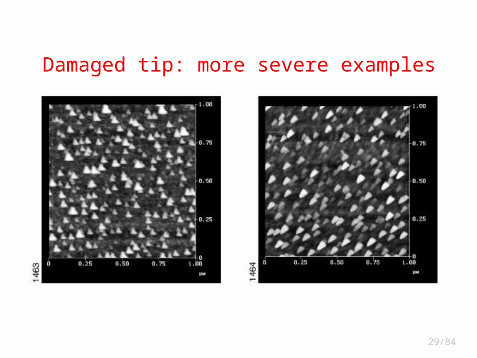
Damaged tip: more severe examples
30/84
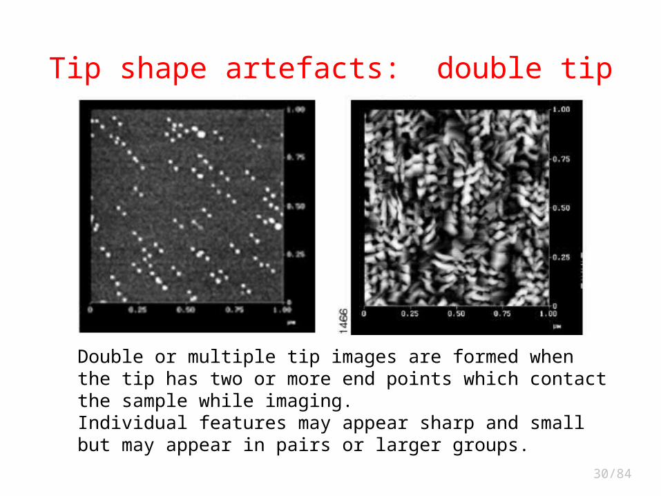
Tip shape artefacts: double tip
Double or multiple tip images are formed when the tip has two or more end points which contact the sample while imaging.Individual features may appear sharp and small but may appear in pairs or larger groups.
31/84
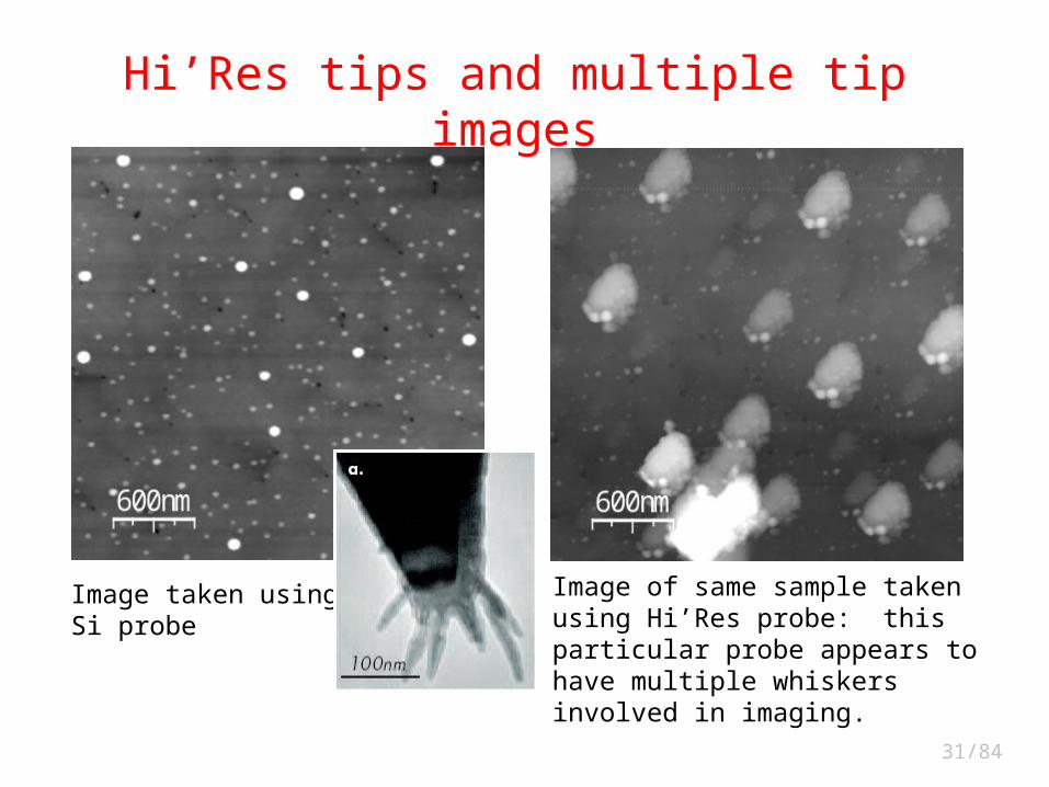
Hi’Res tips and multiple tip images
Image taken using normal Si probe Image of same sample taken using Hi’Res probe: this particular probe appears to have multiple whiskers involved in imaging.
32/84
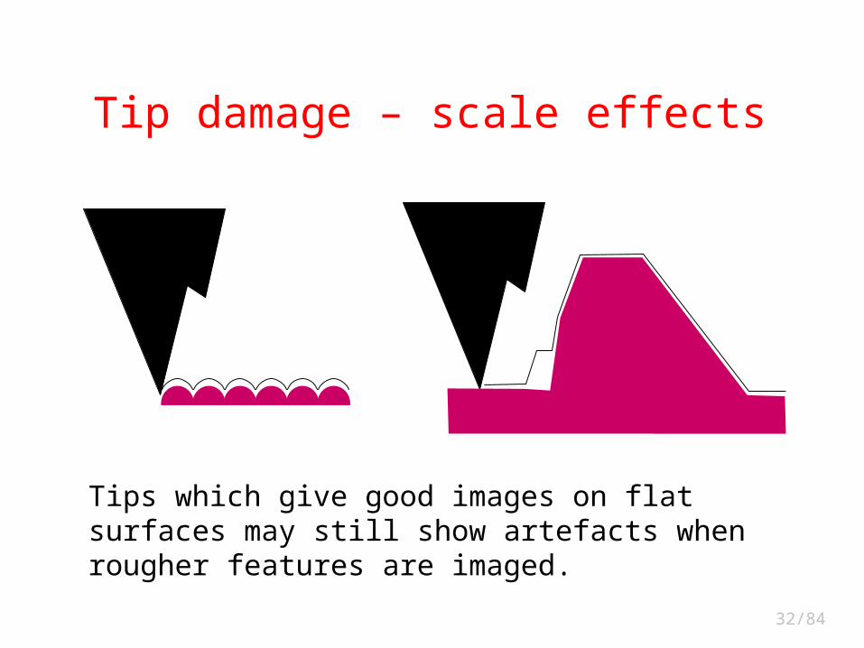
Tip damage – scale effects
Tips which give good images on flat surfaces may still show artefacts when rougher features are imaged.
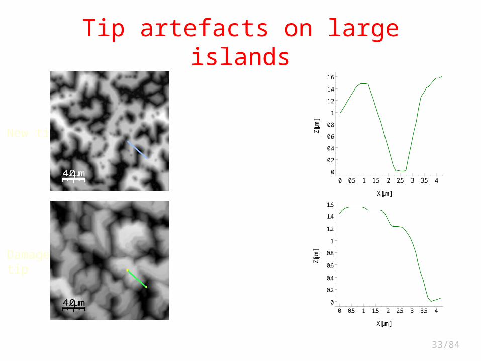
33/84
4.0µm 4.0µm
4.0µm 4.0µm
New tip
Damaged tip
4.0µm
4.0µm0 0.5 1 1.5 2 2.5 3 3.5 4
0
0.2
0.4
0.6
0.8
1
1.2
1.4
1.6
X[µm]
Z[µm
]0 0.5 1 1.5 2 2.5 3 3.5 4
0
0.2
0.4
0.6
0.8
1
1.2
1.4
1.6
X[µm]Z[
µm]
Tip artefacts on large islands
34/84
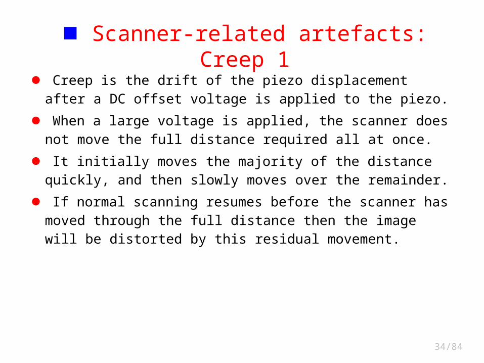
Scanner-related artefacts: Creep 1
Creep is the drift of the piezo displacement after a DC offset voltage is applied to the piezo.
When a large voltage is applied, the scanner does not move the full distance required all at once.
It initially moves the majority of the distance quickly, and then slowly moves over the remainder.
If normal scanning resumes before the scanner has moved through the full distance then the image will be distorted by this residual movement.
35/84
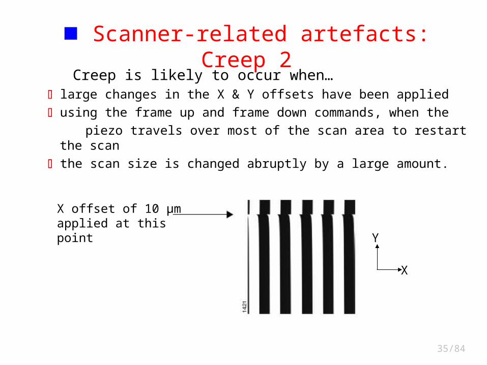
Creep is likely to occur when… large changes in the X & Y offsets have been applied
using the frame up and frame down commands, when the
piezo travels over most of the scan area to restart the scan
the scan size is changed abruptly by a large amount.
X
Y
X offset of 10 µm applied at this point
Scanner-related artefacts: Creep 2
36/84
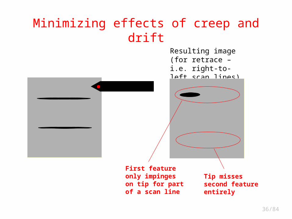
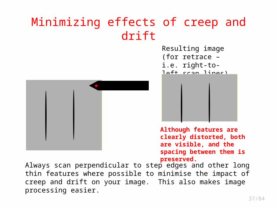
Minimizing effects of creep and drift
Resulting image (for retrace – i.e. right-to-left scan lines)
Tip misses second feature entirely
First feature only impinges on tip for part of a scan line
37/84
Resulting image (for retrace – i.e. right-to-left scan lines)
Although features are clearly distorted, both are visible, and the spacing between them is preserved.
Always scan perpendicular to step edges and other long thin features where possible to minimise the impact of creep and drift on your image. This also makes image processing easier.
Minimizing effects of creep and drift
38/84
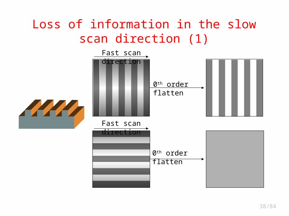
Loss of information in the slow scan direction (1)
0th order flatten
0th order flatten
Fast scan direction
Fast scan direction
39/84
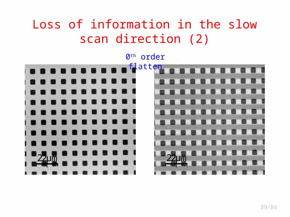
22µm22µm
0th order flatten
Loss of information in the slow scan direction (2)
40/84
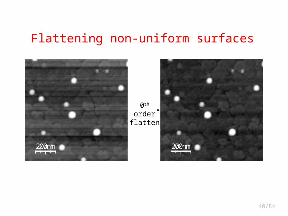
200nm 200nm
0th order flatten
Flattening non-uniform surfaces
41/84
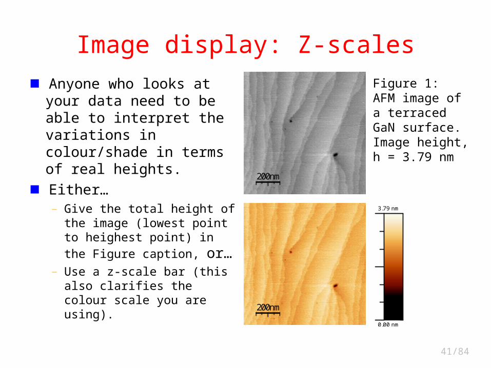
Image display: Z-scales
Anyone who looks at your data need to be able to interpret the variations in colour/shade in terms of real heights.
Either…– Give the total height of the
image (lowest point to heighest point) in the Figure
caption, or…– Use a z-scale bar (this also
clarifies the colour scale you are using).
200nm
Figure 1: AFM image of a terraced GaN surface. Image height, h = 3.79 nm
200nm
3.79 nm
0.00 nm
42/84
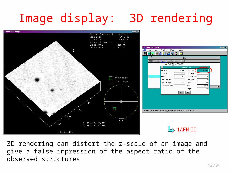
Image display: 3D rendering
3D rendering can distort the z-scale of an image and give a false impression of the aspect ratio of the observed structures
1AFM软件
43/84
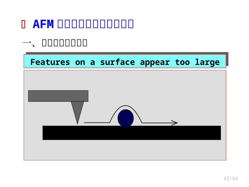
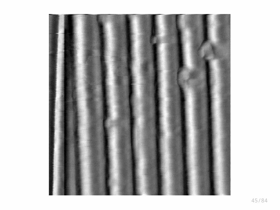
一、测试图像结构偏大Features on a surface appear too largeFeatures on a surface appear too large
AFM 的测试图像畸变失真问题
44/84
45/84
46/84
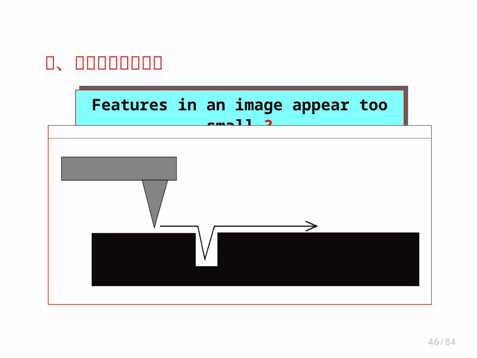
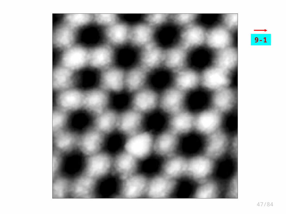
二、测试图像结构偏小
Features in an image appear too small ?Features in an image appear too small ?
47/84
9-1
48/84
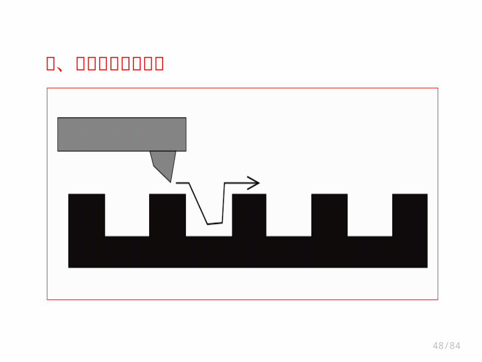
三、测试图像结构失真
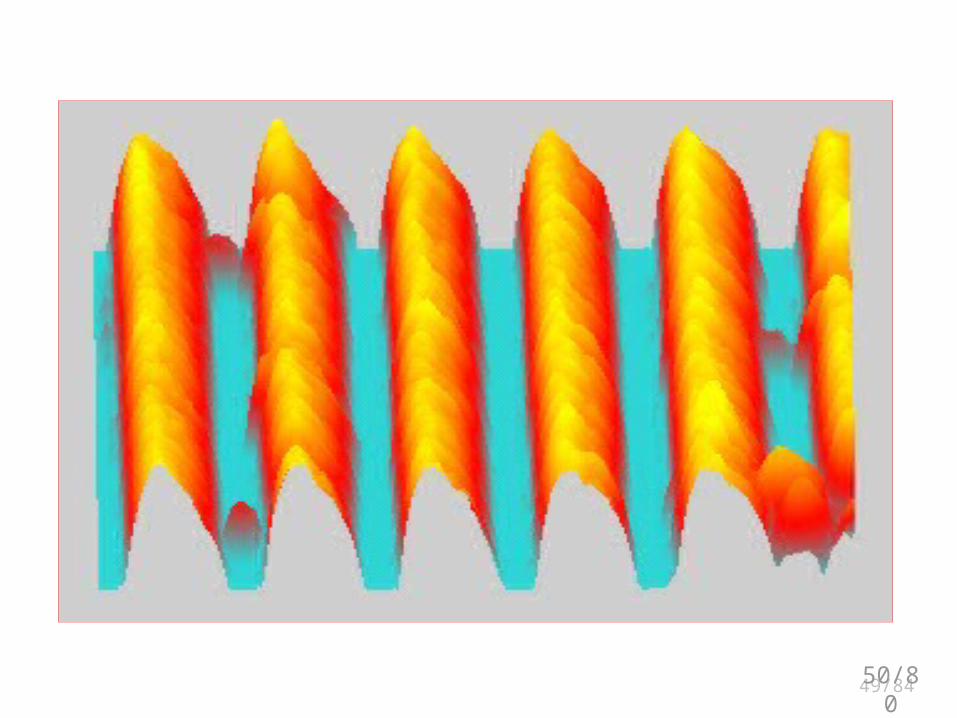
49/8450/80
50/84
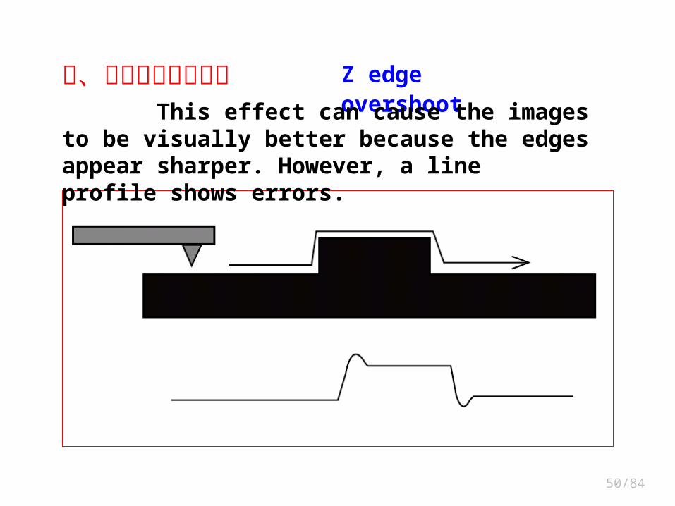
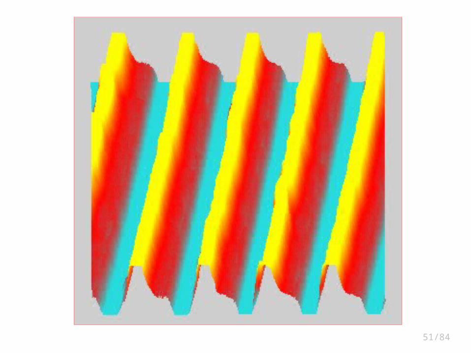
四、测试图像边缘失真 Z edge overshoot This effect can cause the images to be visually better
because the edges appear sharper. However, a line profile shows errors.
51/84
52/84
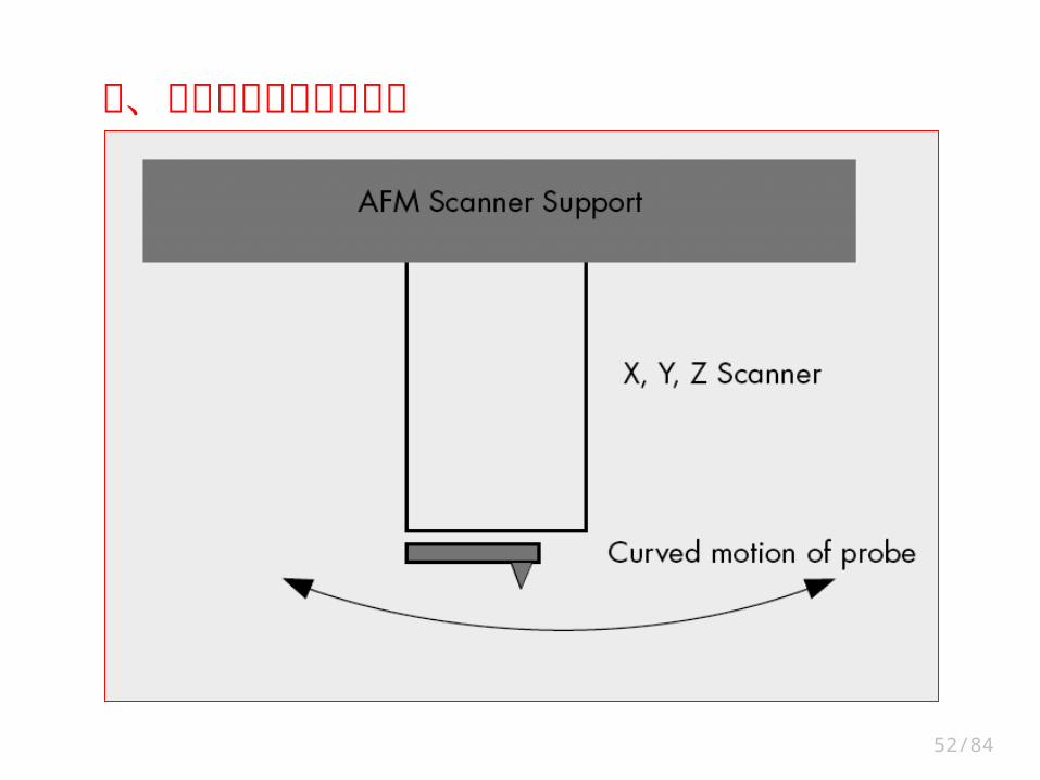
五、扫描器造成的图像失真
53/84
9-2
54/84
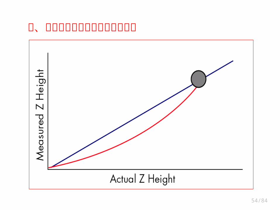
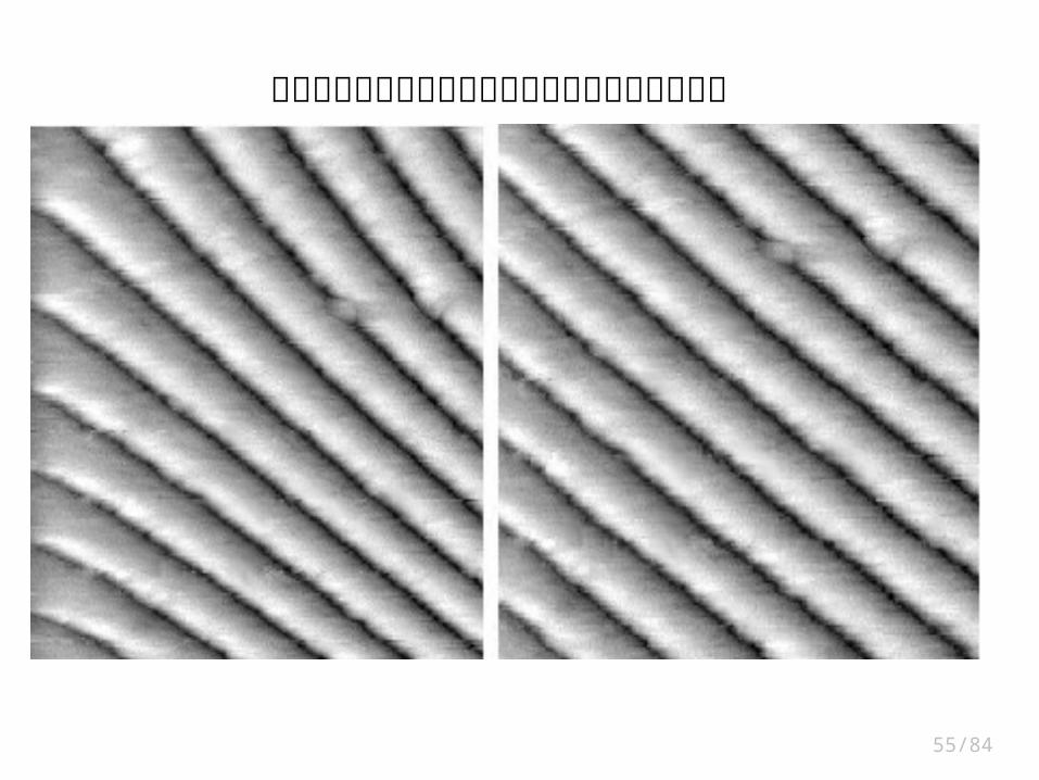
六、压电陶瓷非线性造成的图像失真
55/84
未经校正压电陶瓷扫描获得的光栅图像及软件校正
56/84
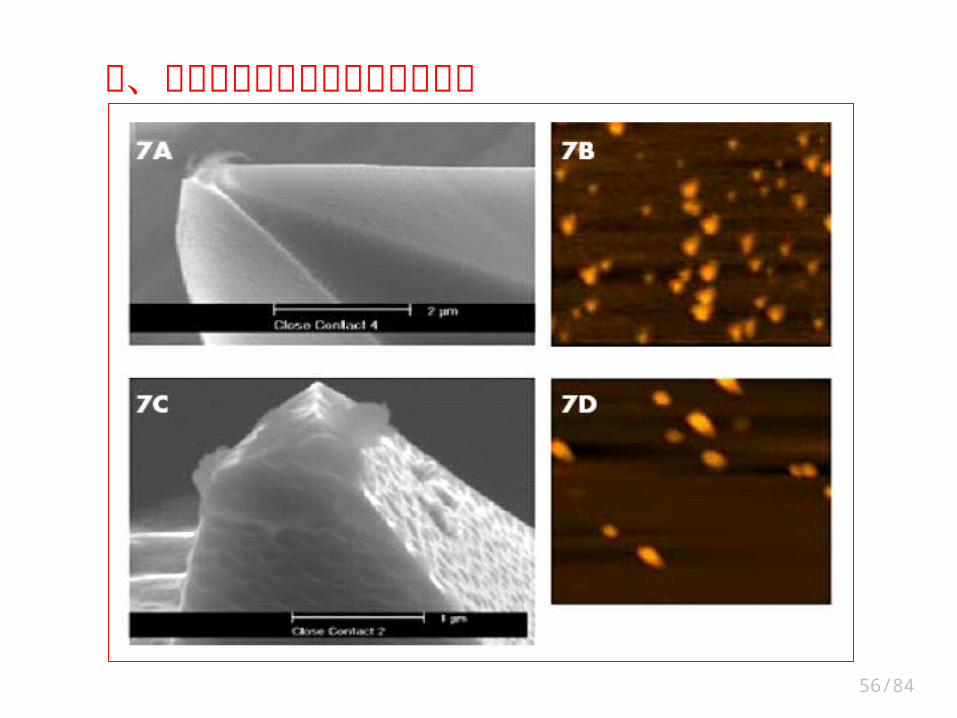
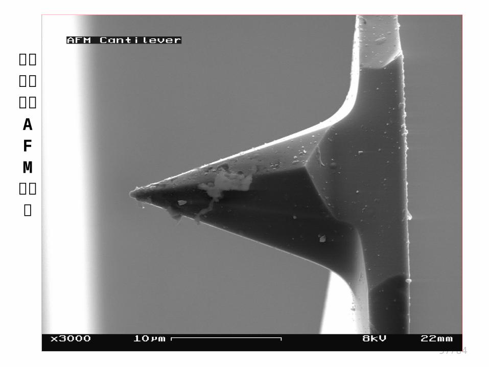
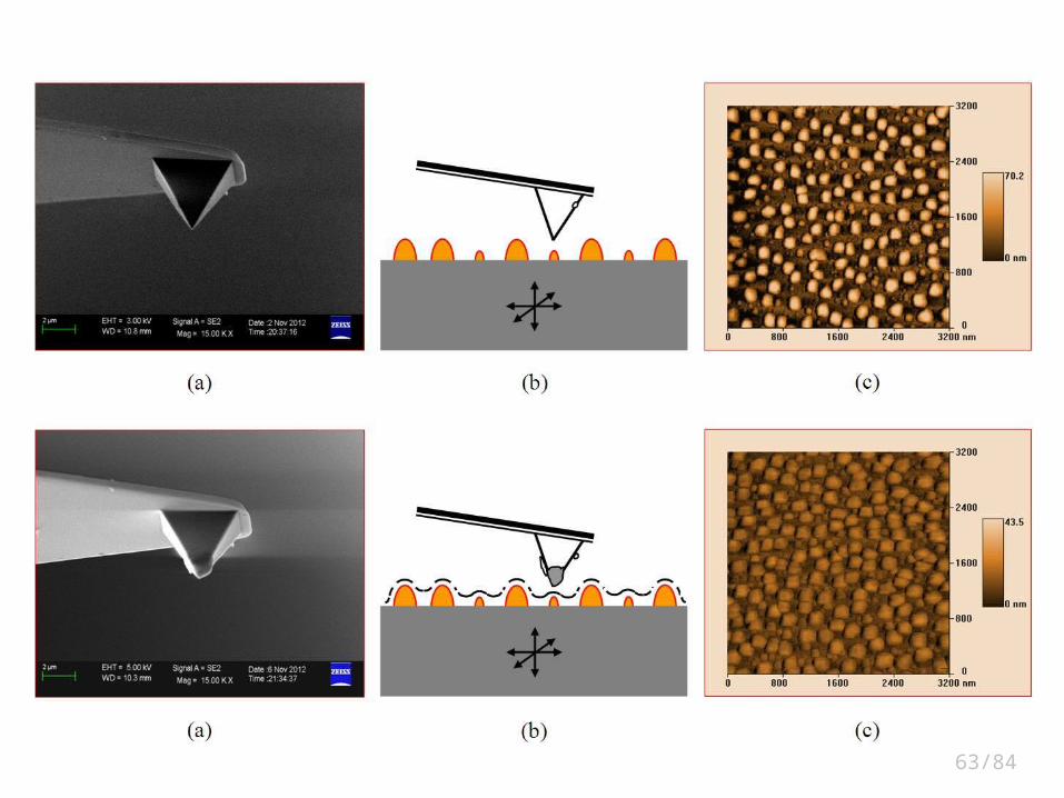
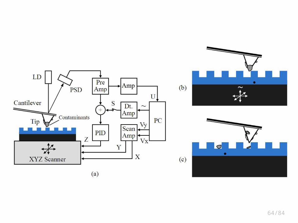
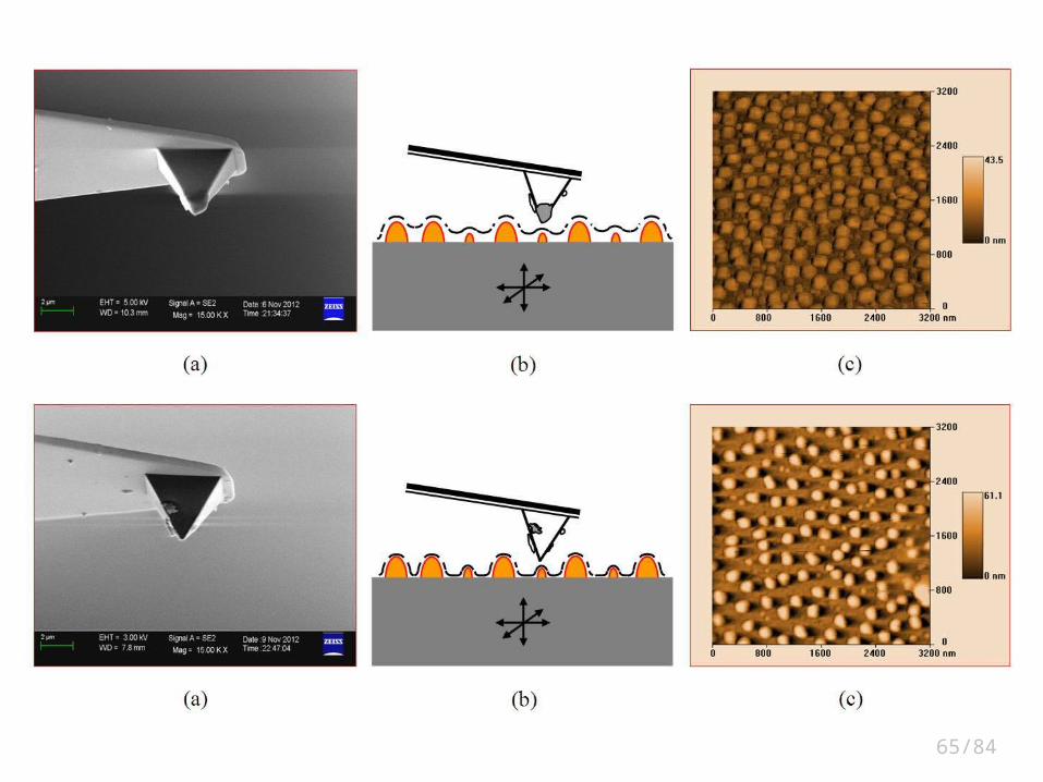
七、微探针针尖污损造成的图像失真
57/84
使用后污损的AFM微探针
58/8470/80
59/84
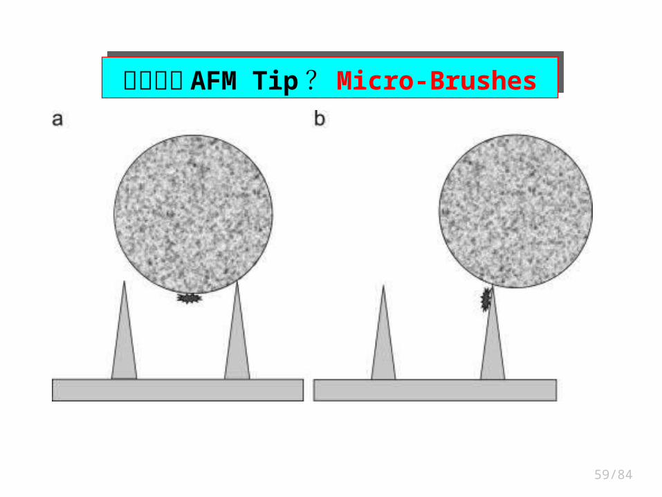
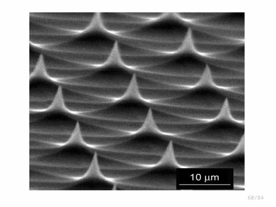
怎样清洗 AFM Tip ? Micro-Brushes怎样清洗 AFM Tip ? Micro-Brushes
60/84
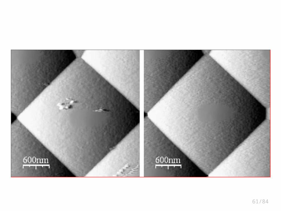
61/84
62/84
如何清洗 AFM Tip ?
63/84
64/84
65/84
66/84
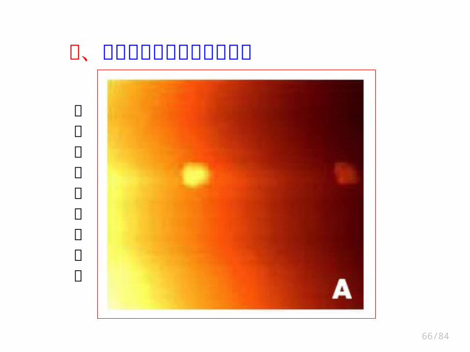
八、畸变与失真图像的处理实例
图像存在倾斜和阴影
67/84
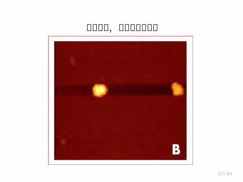
消除倾斜,但阴影带仍存在
68/84
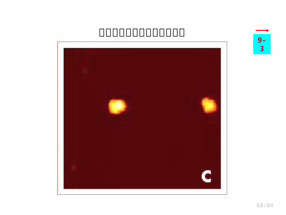
消除倾斜和阴影后的理想图像9-3
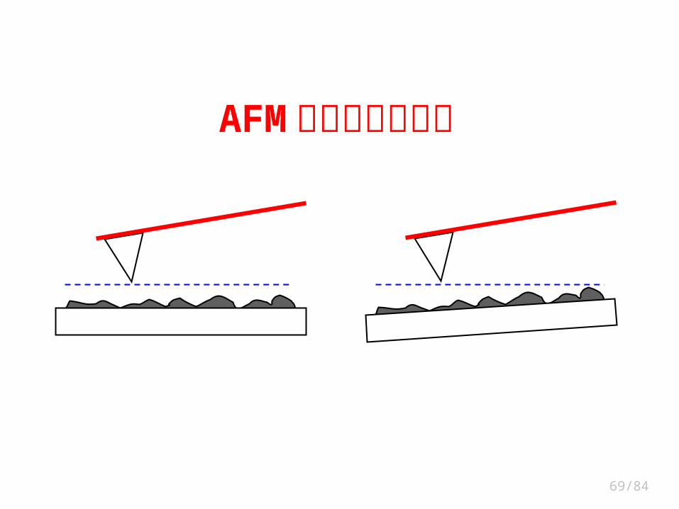
69/84
AFM 图像消倾斜实例
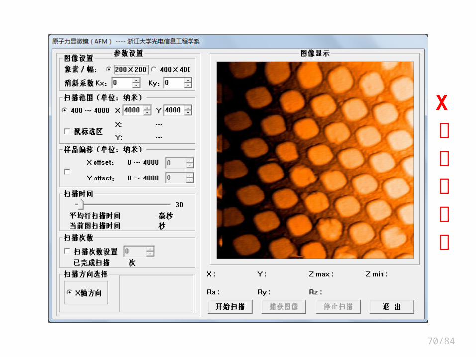
70/84
X方向消倾斜

71/84
X方向消倾斜
72/84
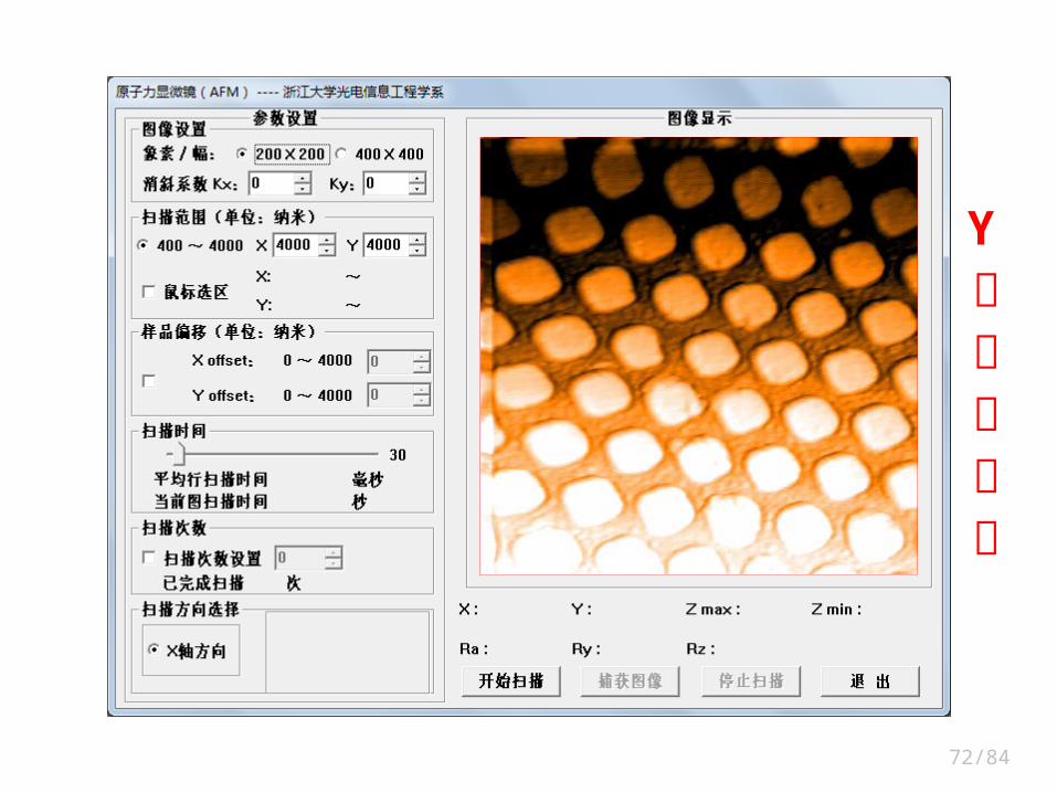
Y方向消倾斜
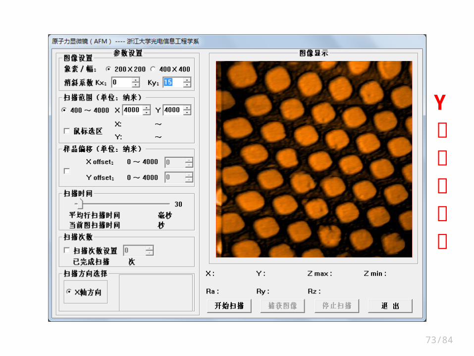
73/84
Y方向消倾斜
74/84
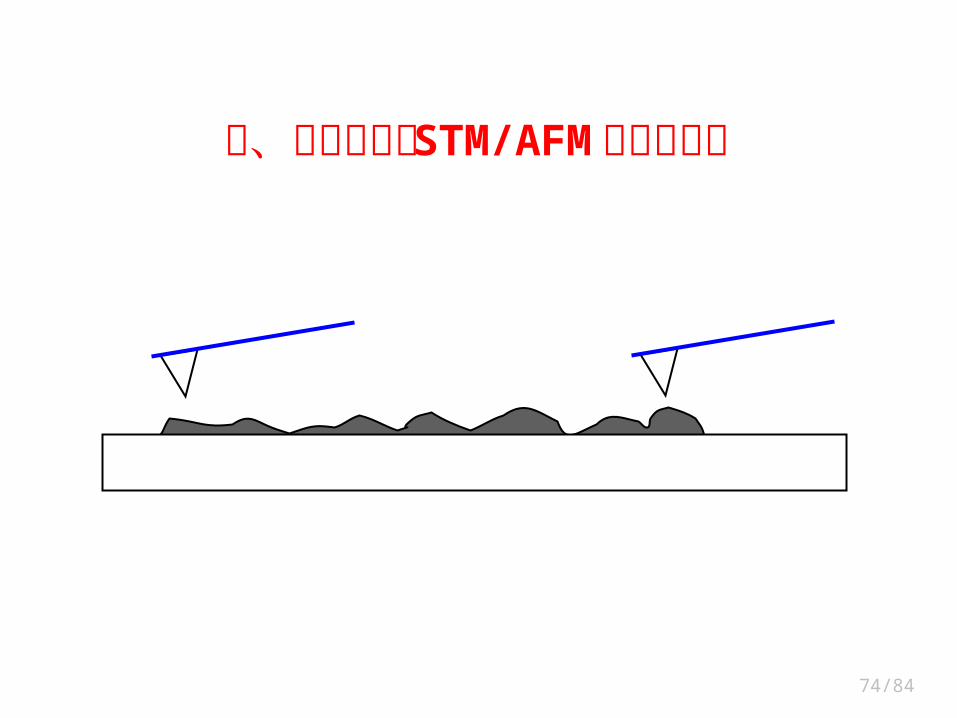
九、扫描惯性对 STM/AFM 图像的影响
75/84
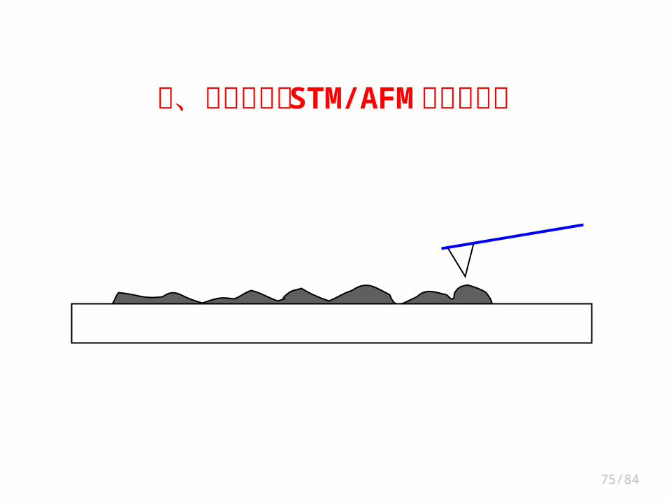
九、扫描惯性对 STM/AFM 图像的影响
76/84
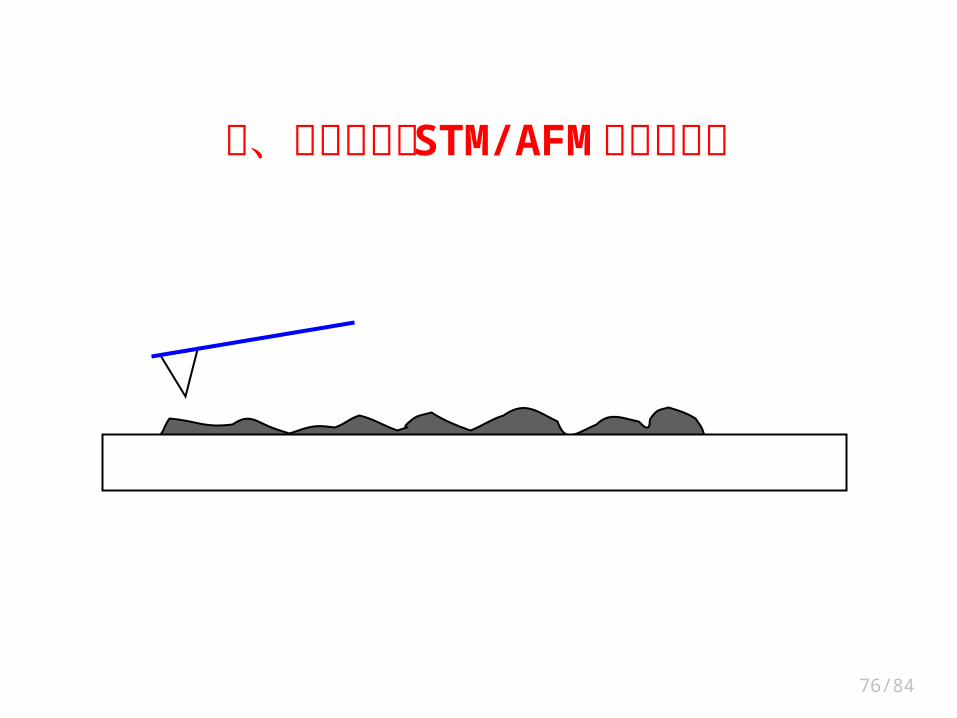
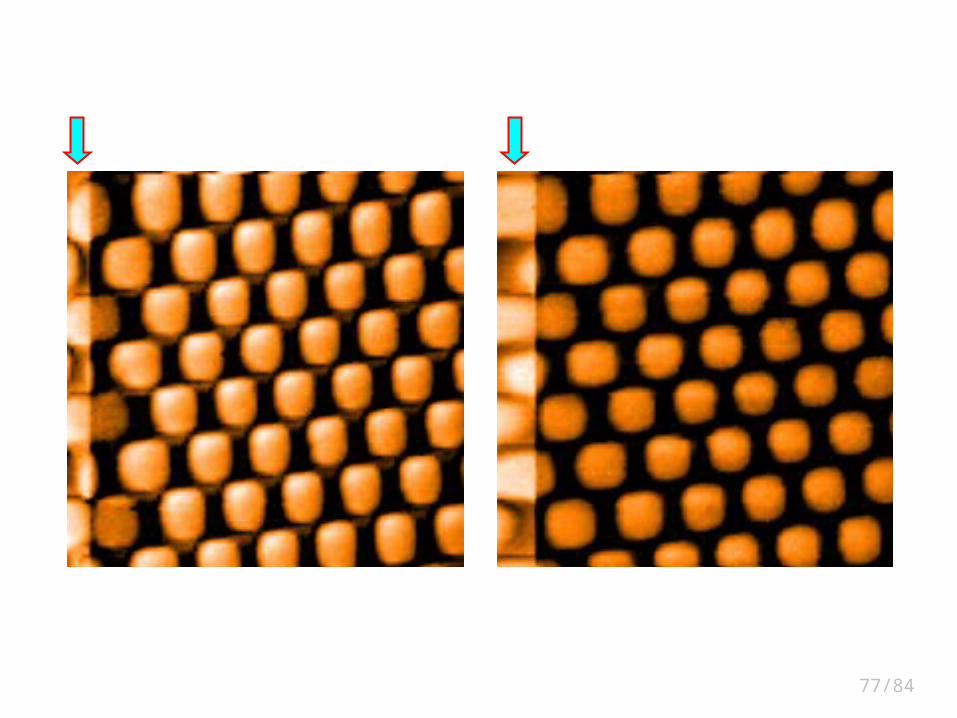
九、扫描惯性对 STM/AFM 图像的影响
77/84
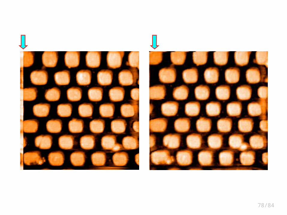
78/84
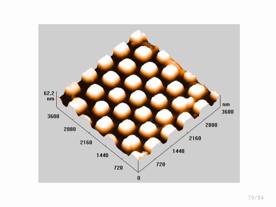
79/84

80/84
To be continuedTo be continued