Embed Size (px)
Citation preview
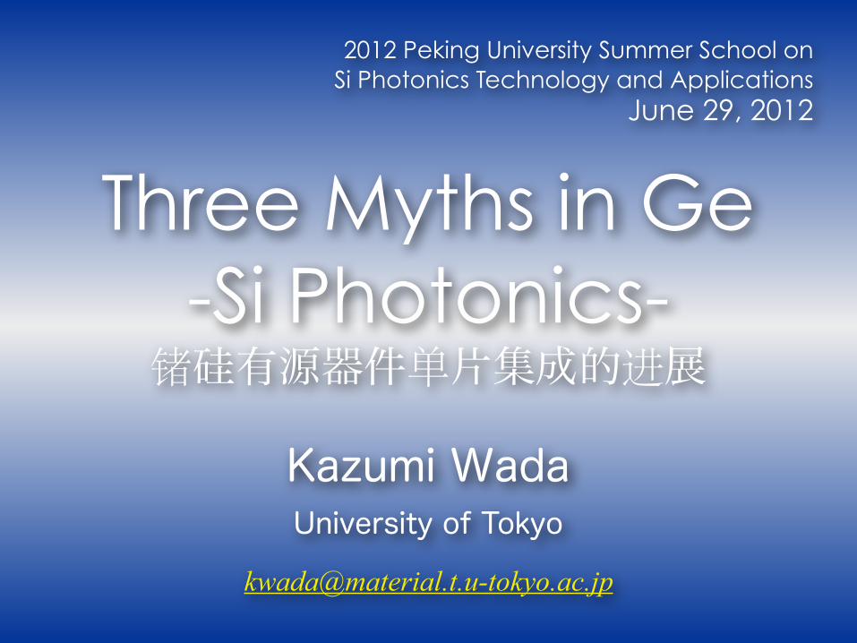
Kazumi WadaUniversity of Tokyo
2012 Peking University Summer School on Si Photonics Technology and Applications
June 29, 2012
Three Myths in Ge-Si Photonics-锗硅有源器件单片集成的进展
Lecture Notes
A Lecturer has designated this material as copyright-protected.
•Material protected by copyright has restrictions on usage and reproduction, which may be subject to Fair Use exceptions for nonprofit, educational purposes under limited circumstances.
•You should acknowledge that this material may be protected by copyright law and its usage may be restricted.
2
3
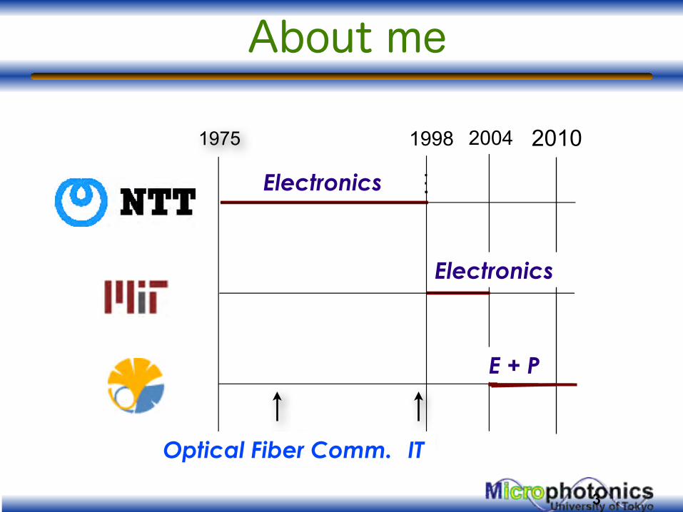
About me
1975
光通信 IT
1998 2004
エレクトロニクス, E
フォトニクス, P
E+P
2010
Electronics
Electronics
E + P
Electronics
Optical Fiber Comm. IT
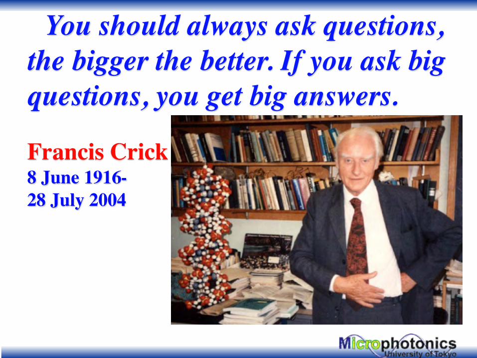
You should always ask questions, the bigger the better. If you ask big questions, you get big answers.
Francis Crick8 June 1916-28 July 2004
Outline
• Introduction
• High performance computing and communication
• Problems and Solutions
• Three myths in Ge research in Si photonics
• Epitaxy, detection limit, and lasing
• Summary
5
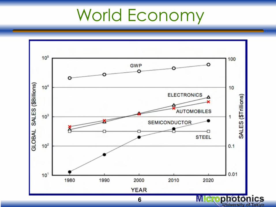
World Economy
6
7
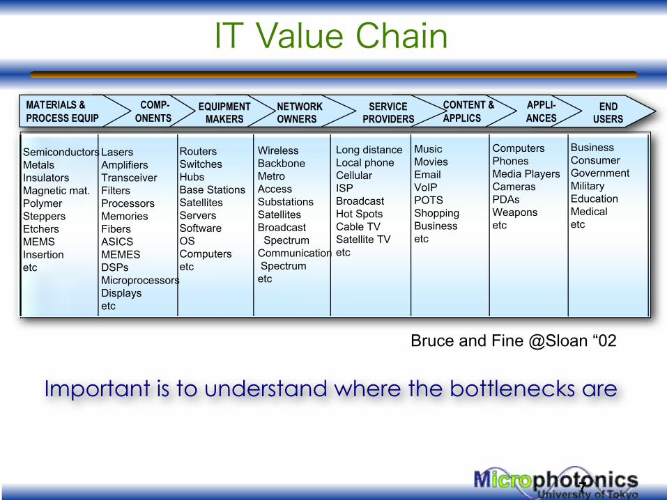
Important is to understand where the bottlenecks are
END USERS
CONTENT & APPLICS
APPLI-ANCES
SERVICE PROVIDERS
NETWORKOWNERS
EQUIPMENTMAKERS
COMP-ONENTS
MATERIALS &PROCESS EQUIP
SemiconductorsMetals InsulatorsMagnetic mat.PolymerSteppersEtchersMEMSInsertionetc
LasersAmplifiersTransceiverFiltersProcessorsMemoriesFibersASICSMEMESDSPsMicroprocessorsDisplaysetc
RoutersSwitchesHubsBase StationsSatellitesServersSoftwareOSComputersetc
WirelessBackboneMetroAccessSubstationsSatellitesBroadcast SpectrumCommunication Spectrumetc
Long distanceLocal phoneCellularISPBroadcastHot Spots Cable TVSatellite TVetc
MusicMoviesEmailVoIPPOTSShoppingBusinessetc
ComputersPhonesMedia PlayersCamerasPDAsWeaponsetc
BusinessConsumerGovernmentMilitaryEducationMedicaletc
Bruce and Fine @Sloan “02
IT Value Chain
8
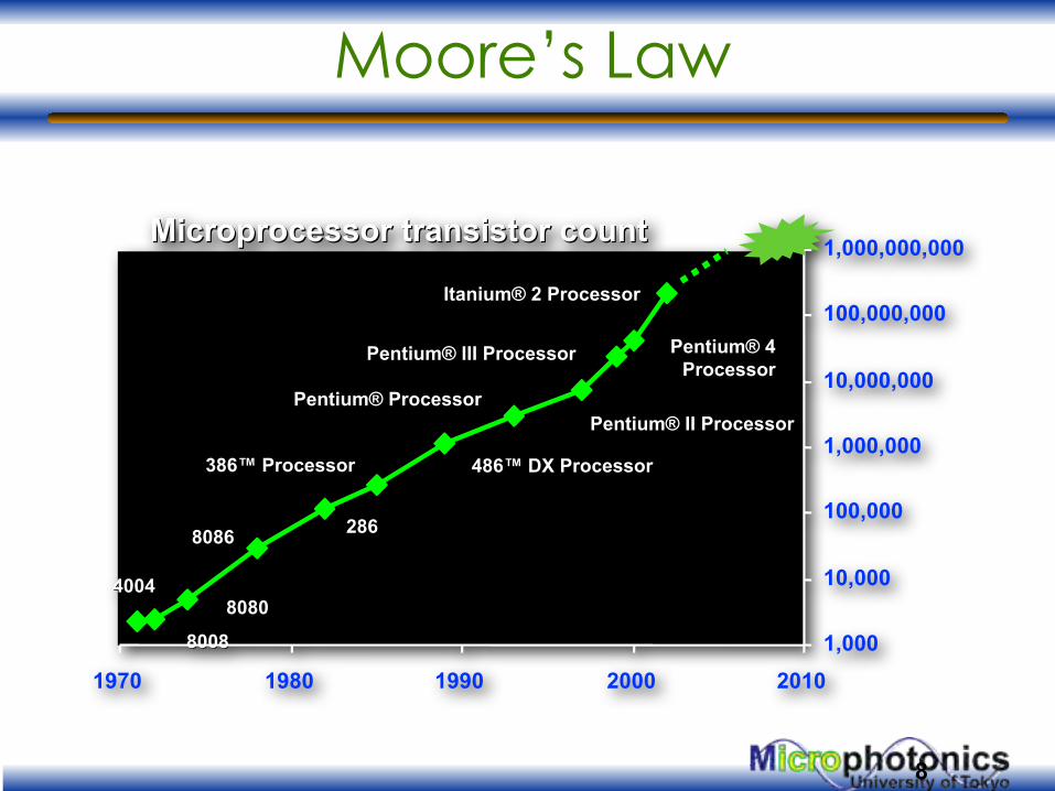
Moore’s Law
4004400480808080
80868086
80088008
PentiumPentium®® Processor Processor
486486™™ DX Processor DX Processor386386™™ Processor Processor
286286
PentiumPentium®® II Processor II Processor
PentiumPentium®® III Processor III Processor PentiumPentium®® 4 4ProcessorProcessor
ItaniumItanium®® 2 Processor 2 Processor
1,000
10,000
100,000
1,000,000
10,000,000
100,000,000
1,000,000,000
1970 1980 1990 2000 2010
Microprocessor transistor countMicroprocessor transistor count
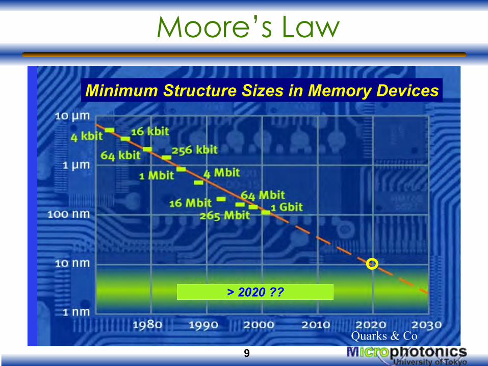
Moore’s Law
9Quarks & Co
Minimum Structure Sizes in Memory Devices
> 2020 ??
10
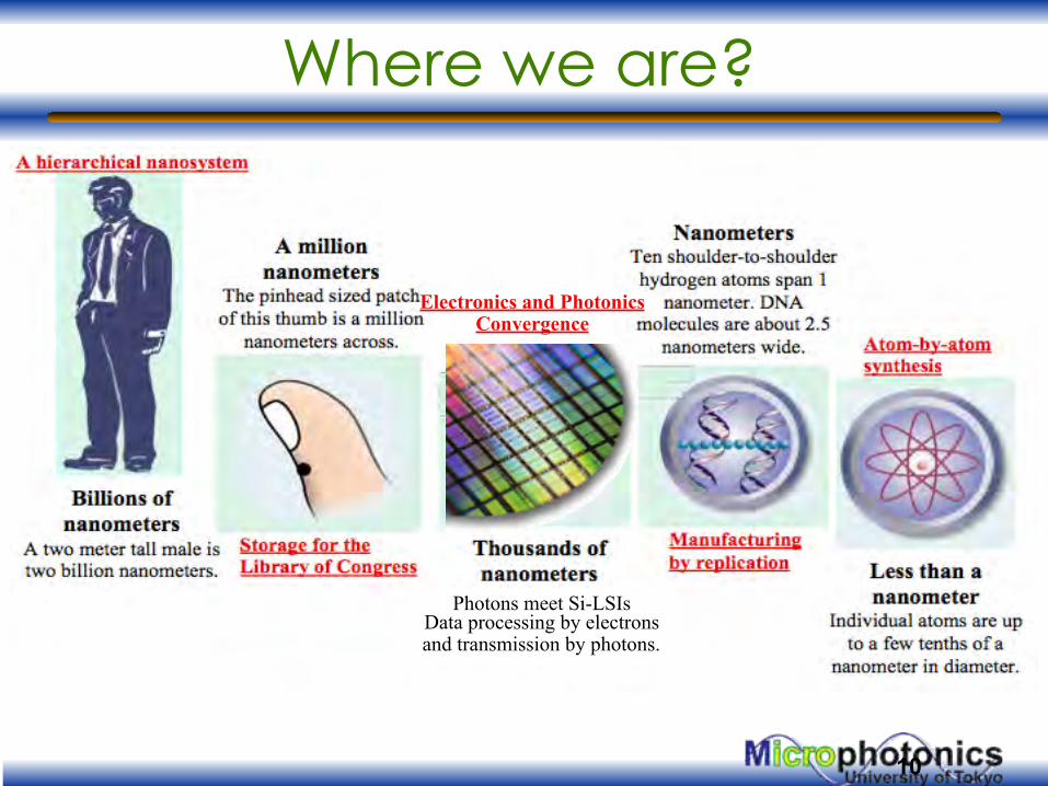
Where we are?
Photons meet Si-LSIs Data processing by electrons and transmission by photons.
Electronics and Photonics Convergence
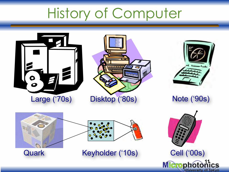
Large (‘70s) Disktop (‘80s) Note (‘90s)
Cell (‘00s)Keyholder (‘10s)Quark
History of Computer
11
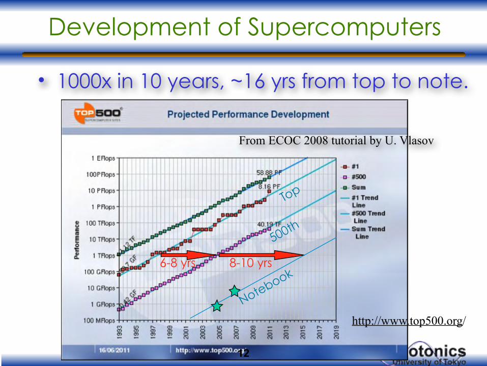
Development of Supercomputers
• 1000x in 10 years, ~16 yrs from top to note.
6-8 yrs 8-10 yrs
500th
Top
Notebook
From ECOC 2008 tutorial by U. Vlasov
http://www.top500.org/
12
• However, everything has limitation in human history.
13
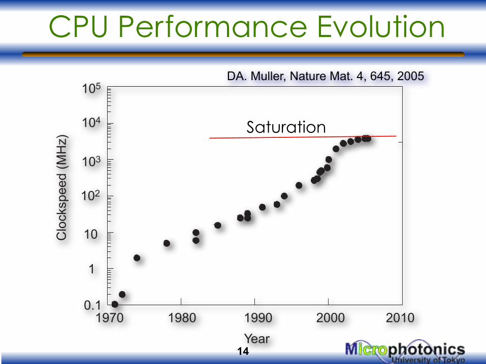
CPU Performance Evolution
1970 1980 1990 2000 2010
105
104
103
102
10
1
0.1
Clo
cksp
eed
(MH
z)
Year
DA. Muller, Nature Mat. 4, 645, 2005
14
Saturation
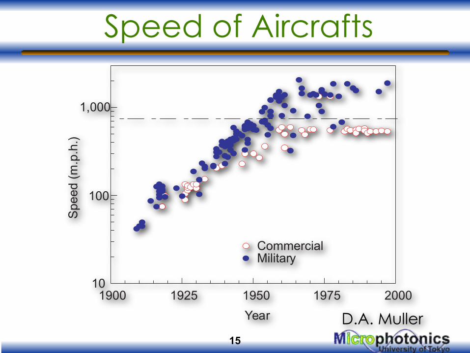
Speed of Aircrafts
15
1900 1925 1950 1975 2000
Year
CommercialMilitary
1,000
100
10
Spe
ed (
m.p
.h.)
D.A. Muller
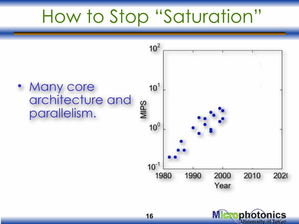
How to Stop “Saturation”
• Many core architecture and parallelism.
16
• The enhancement is limited by a fraction must have serially performed.
Amdahl’s Law
17€
Overall speedup =1
F +1− FN
,
where F - fraction of a program to serially perform, N - number of cores
G.M. Amdahl, In AFIPS Conference Proceedings vol. 30 AFIPS Press, Reston, Va., 1967, pp. 483.
5%
10%
20%
50%
F=0%
18
10-2
100
102
104
106
108
1010
1012
1014
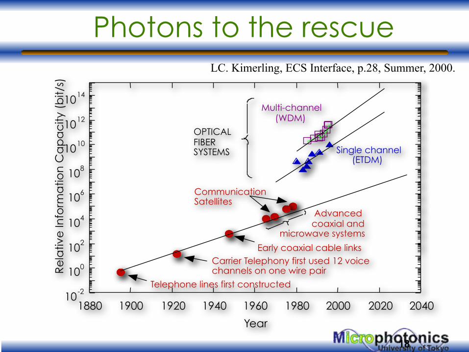
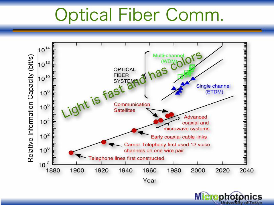
1880 1900 1920 1940 1960 1980 2000 2020 2040
Re
lativ
e In
form
atio
n C
ap
ac
ity (
bit/
s)
Year
Telephone lines first constructed
Carrier Telephony first used 12 voicechannels on one wire pair
Early coaxial cable links
Advanced coaxial and
microwave systems
CommunicationSatellites
Single channel (ETDM)
Multi-channel(WDM)
OPTICAL FIBER SYSTEMS
Photons to the rescueLC. Kimerling, ECS Interface, p.28, Summer, 2000.
Short Summary
• HPC gets faster exponentially. • Top to notebook seems ~16 years.
• Optics is “MUST HAVE” on Si to suppress “saturation”. • On-chip DWDM should be the clue.
• The key is Light emitter (EMT), modulator(MOD), detector(DET), multiplexor/demultiplexor(MUX/DEMUX) on a chip.
19
20
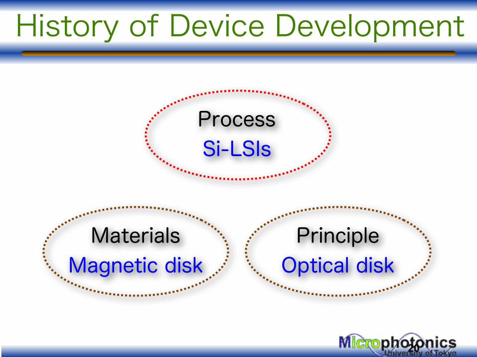
History of Device Development
ProcessSi-LSIs
MaterialsMagnetic disk
PrincipleOptical disk
21
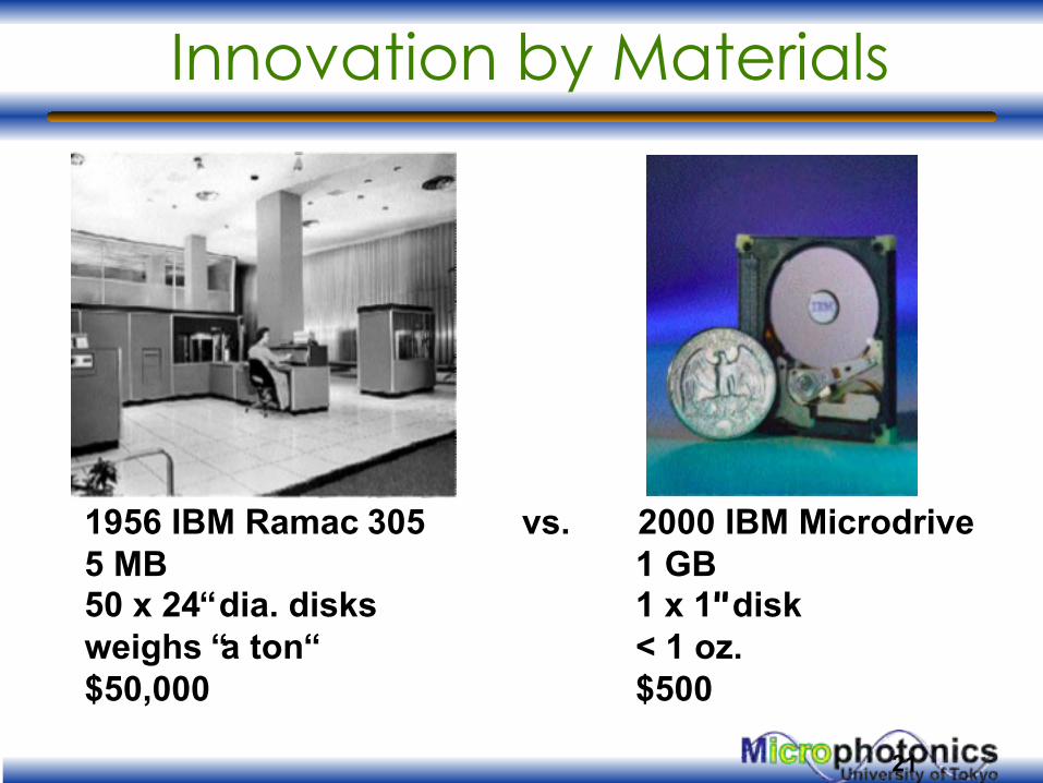
Innovation by Materials
1956 IBM Ramac 305 vs. 2000 IBM Microdrive5 MB 1 GB50 x 24“ dia. disks 1 x 1”“ diskweighs “a ton“ < 1 oz.$50,000 $500
22
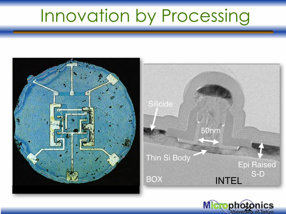
Innovation by Processing
INTEL
23
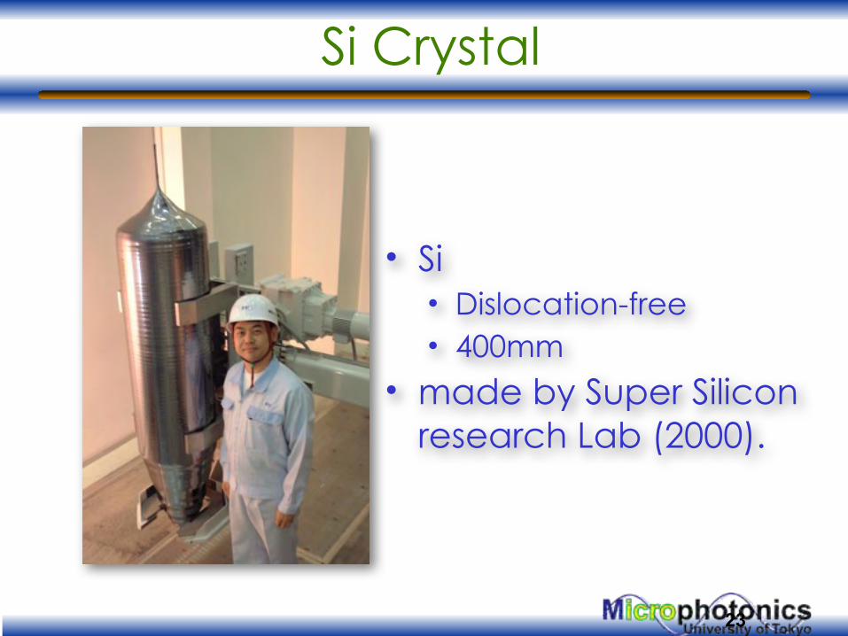
Si Crystal
• Si• Dislocation-free• 400mm
• made by Super Silicon research Lab (2000).
24
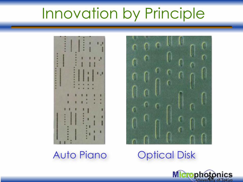
Innovation by Principle
Auto Piano Optical Disk
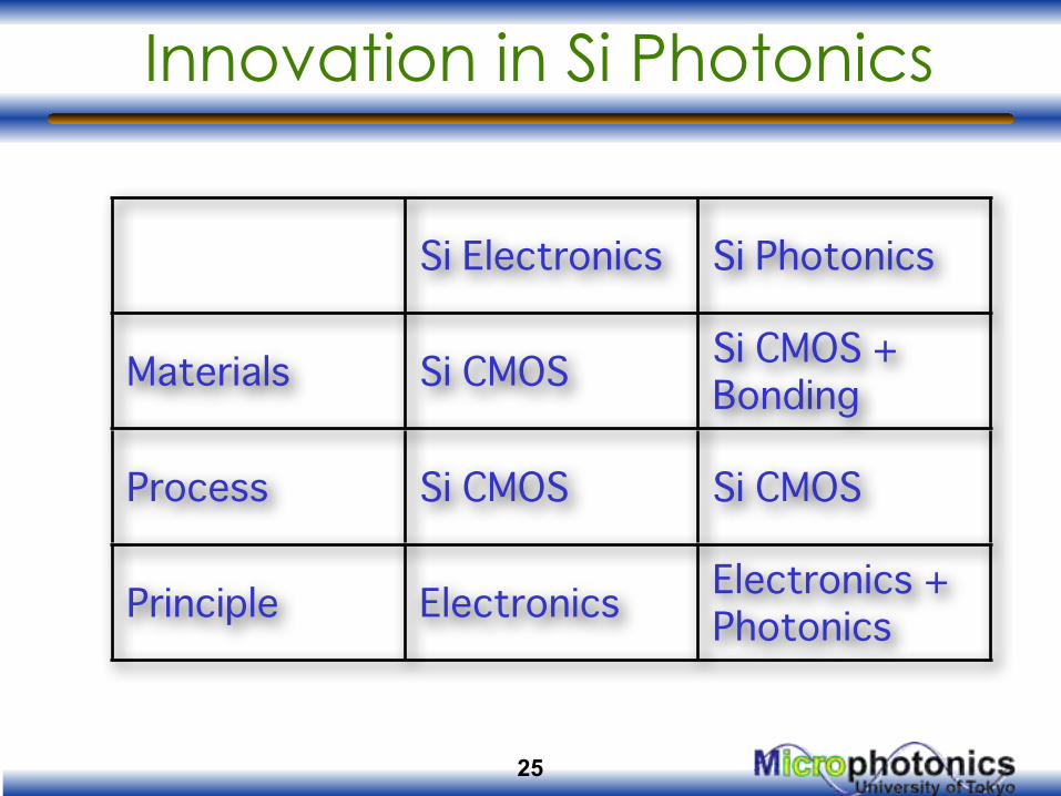
Innovation in Si Photonics
25
Si Electronics Si Photonics
Materials Si CMOSSi CMOS + Bonding
Process Si CMOS Si CMOS
Principle ElectronicsElectronics + Photonics
Electronics + Photonics
• Current tartget
• Signal processing by electronics (transistors)
• Signal transmission by photonics
• Future
• Both by photonics
26
27
Optical Fiber Comm.
10-2
100
102
104
106
108
1010
1012
1014
1880 1900 1920 1940 1960 1980 2000 2020 2040
Relat
ive In
form
ation
Cap
acity
(bit/s
)
Year
Telephone lines first constructed
Carrier Telephony first used 12 voicechannels on one wire pair
Early coaxial cable links
Advanced coaxial and
microwave systems
CommunicationSatellites
Single channel (ETDM)
Multi-channel(WDM)
OPTICAL FIBER SYSTEMS
Rel
ativ
e In
form
atio
n C
apac
ity (b
it/s)
Light is f
ast and has colors
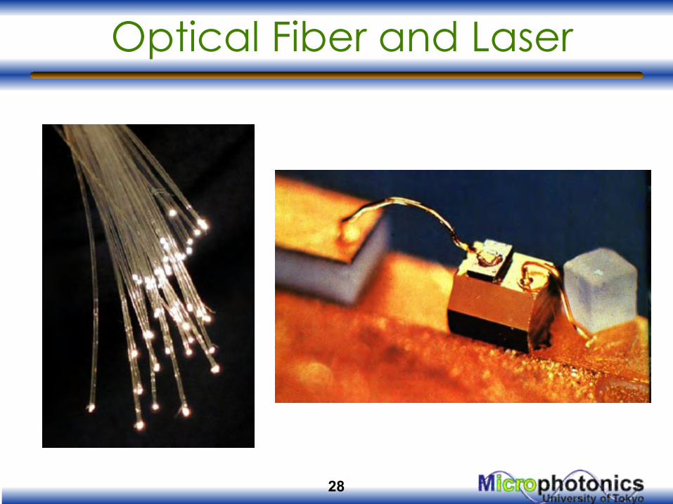
Optical Fiber and Laser
28
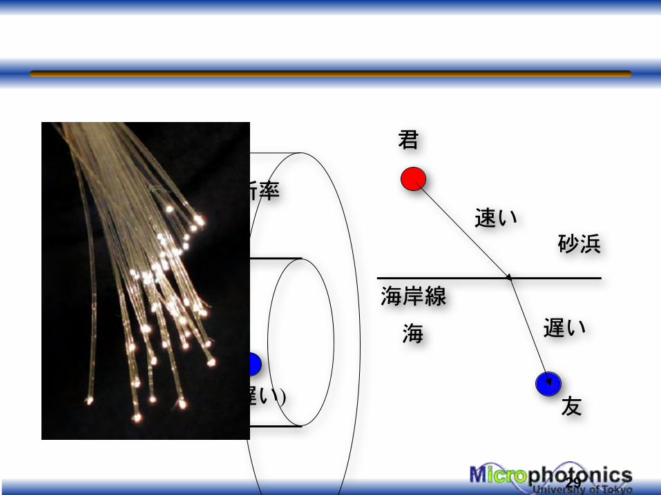
29
砂浜
海
海岸線
君
友
遅い
速い
高屈折率(遅い)
低屈折率
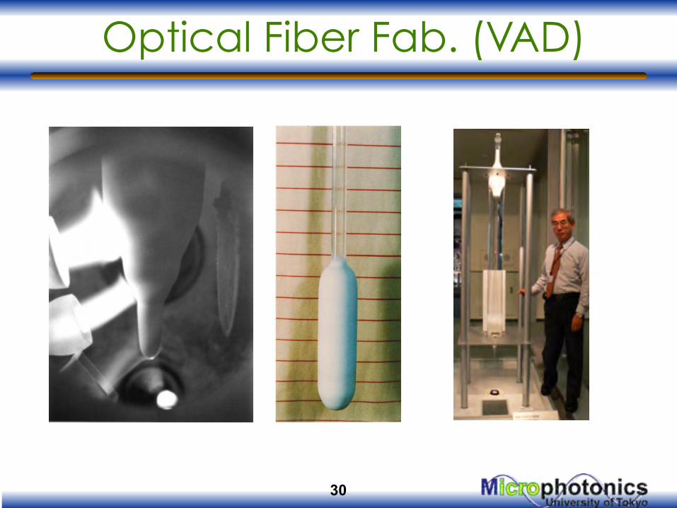
Optical Fiber Fab. (VAD)
30
31
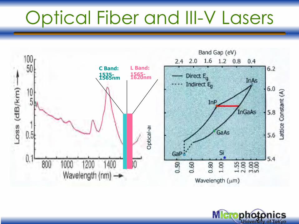
Optical Fiber and III-V Lasers
C Band:1535-1565nm
L Band:1565-1620nm
32
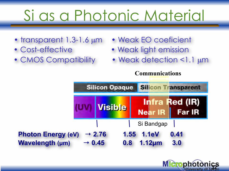
Photon Energy (eV) → 2.76 1.55 1.1eV 0.41Wavelength (µm) → 0.45 0.8 1.12µm 3.0
Si Bandgap
• Weak EO coeficient• transparent 1.3-1.6 μm• Cost-effective • Weak light emission• CMOS Compatibility • Weak detection <1.1 μm
Communications
Si as a Photonic Material
33
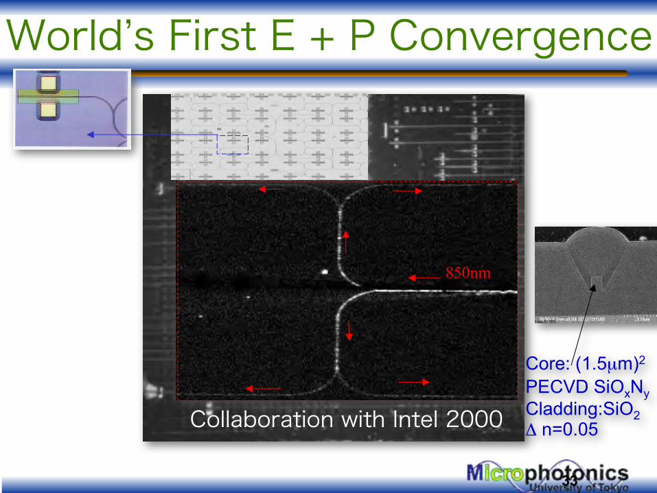
World’s First E + P Convergence
R=800um
850nm
Core: (1.5µm)2
PECVD SiOxNyCladding:SiO2 Δ n=0.05Collaboration with Intel 2000
34
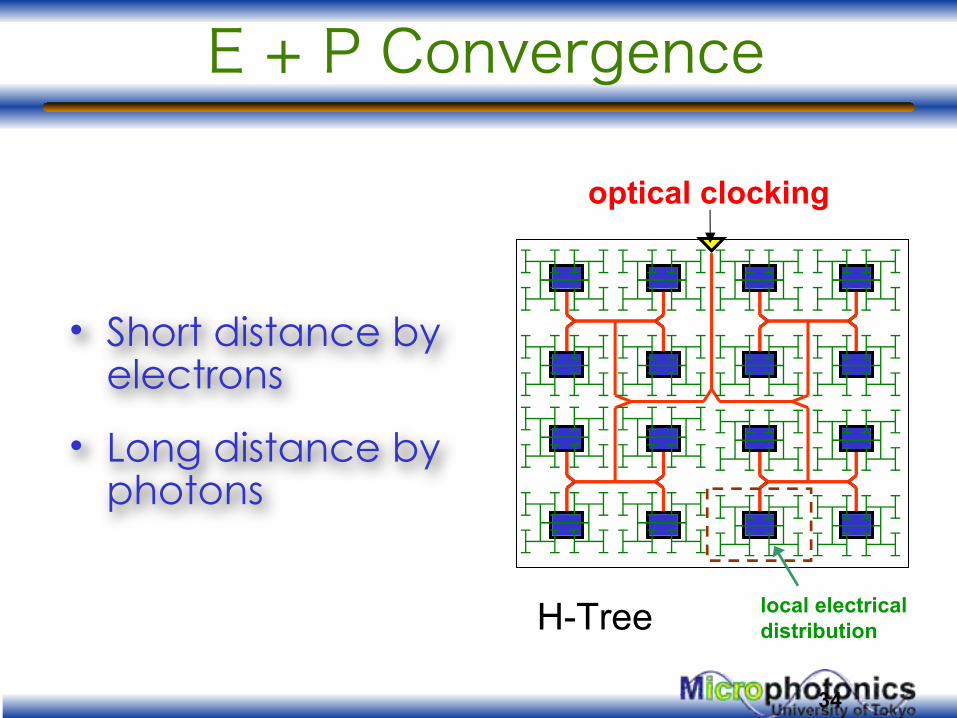
E + P Convergence
• Short distance by electrons
• Long distance by photons
optical clocking
local electricaldistributionH-Tree
35
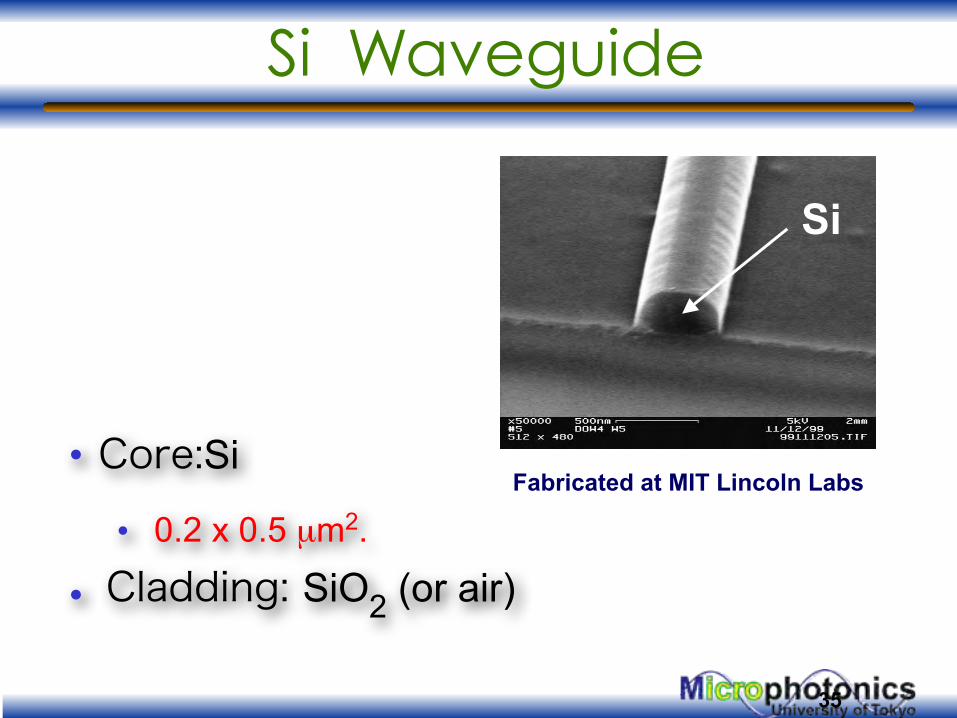
Si Waveguide
• Core:Si
• 0.2 x 0.5 µm2.
• Cladding: SiO2 (or air)
Fabricated at MIT Lincoln Labs
Si
36
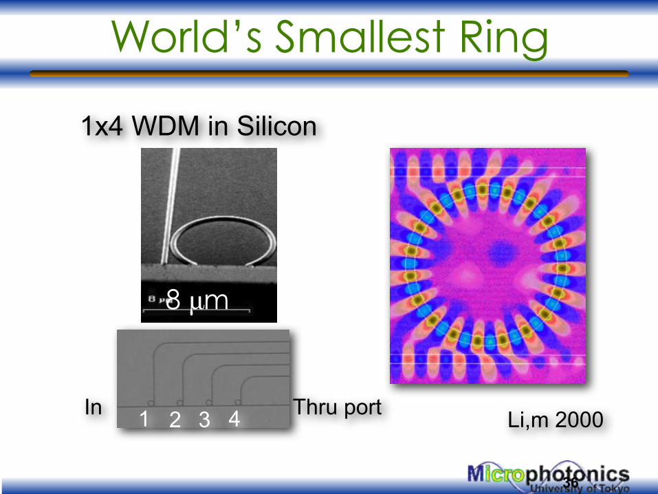
World’s Smallest Ring
1 2 3 4
8 μm
In Li,m 2000Thru port
1x4 WDM in Silicon
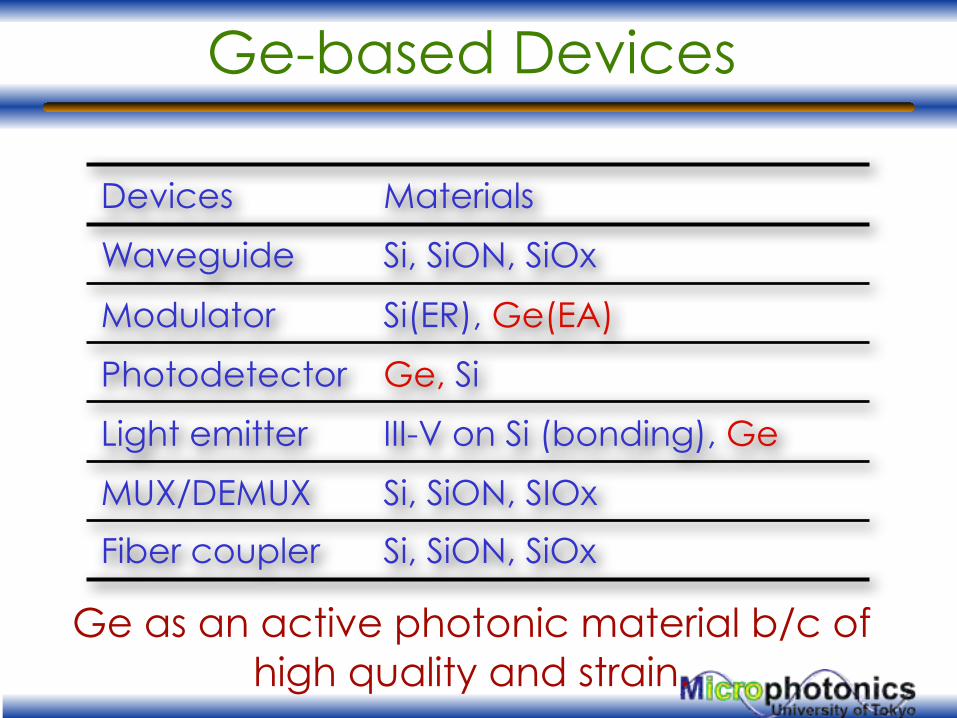
Ge-based Devices
Devices Materials
Waveguide Si, SiON, SiOx
Modulator Si(ER), Ge(EA)
Photodetector Ge, Si
Light emitter III-V on Si (bonding), Ge
MUX/DEMUX Si, SiON, SIOx
Fiber coupler Si, SiON, SiOx
Ge as an active photonic material b/c ofhigh quality and strain.
Intermission
38
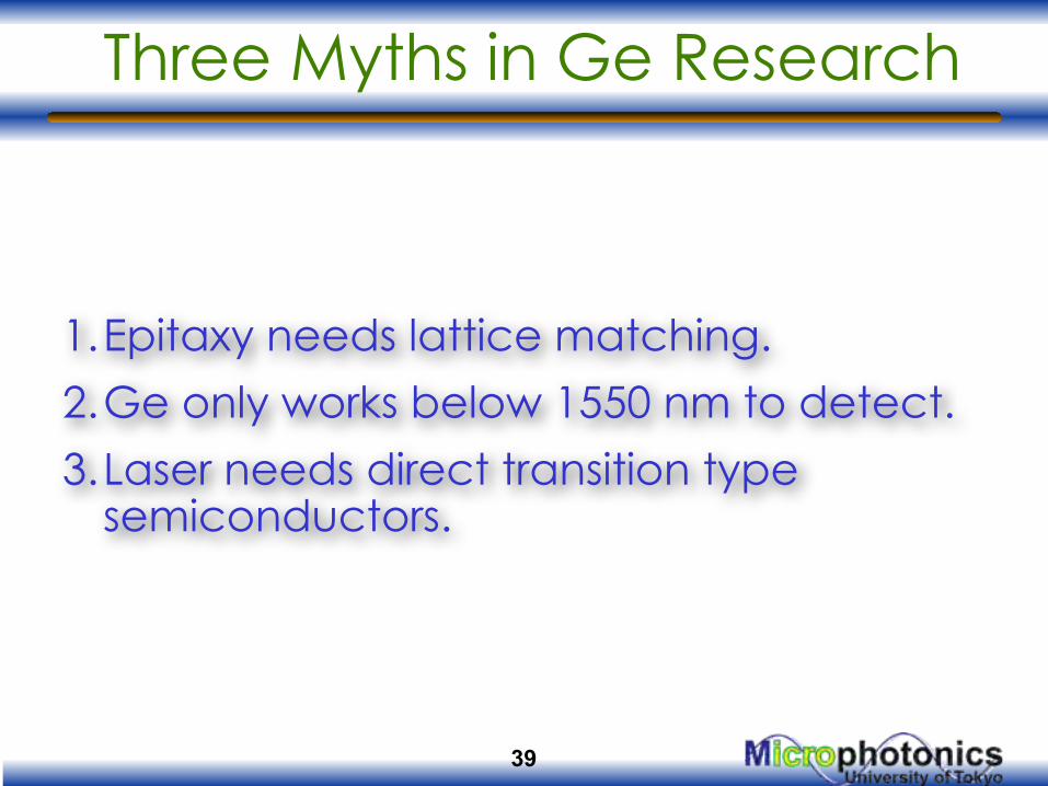
Three Myths in Ge Research
1.Epitaxy needs lattice matching.
2.Ge only works below 1550 nm to detect.
3.Laser needs direct transition type semiconductors.
39
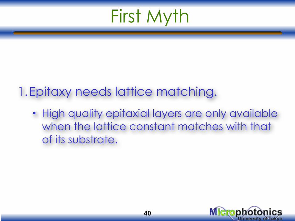
First Myth
1.Epitaxy needs lattice matching.
• High quality epitaxial layers are only available when the lattice constant matches with that of its substrate.
40
41
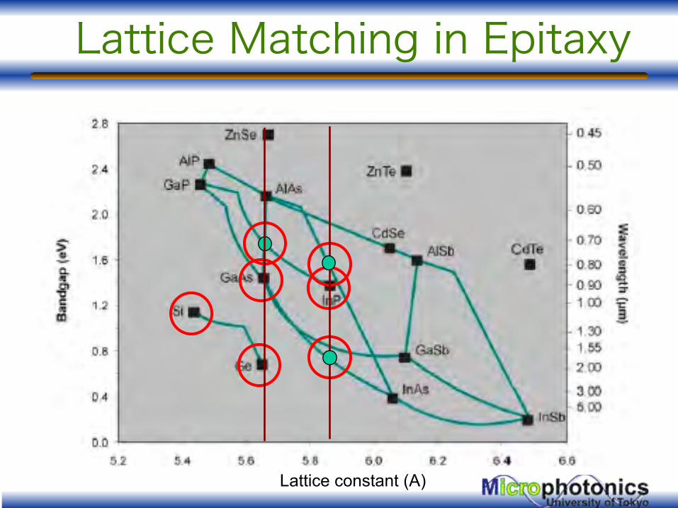
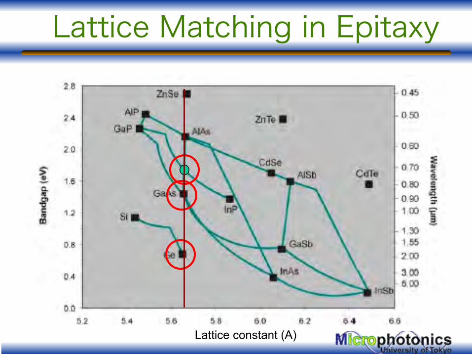
Lattice Matching in Epitaxy
Lattice constant (A)
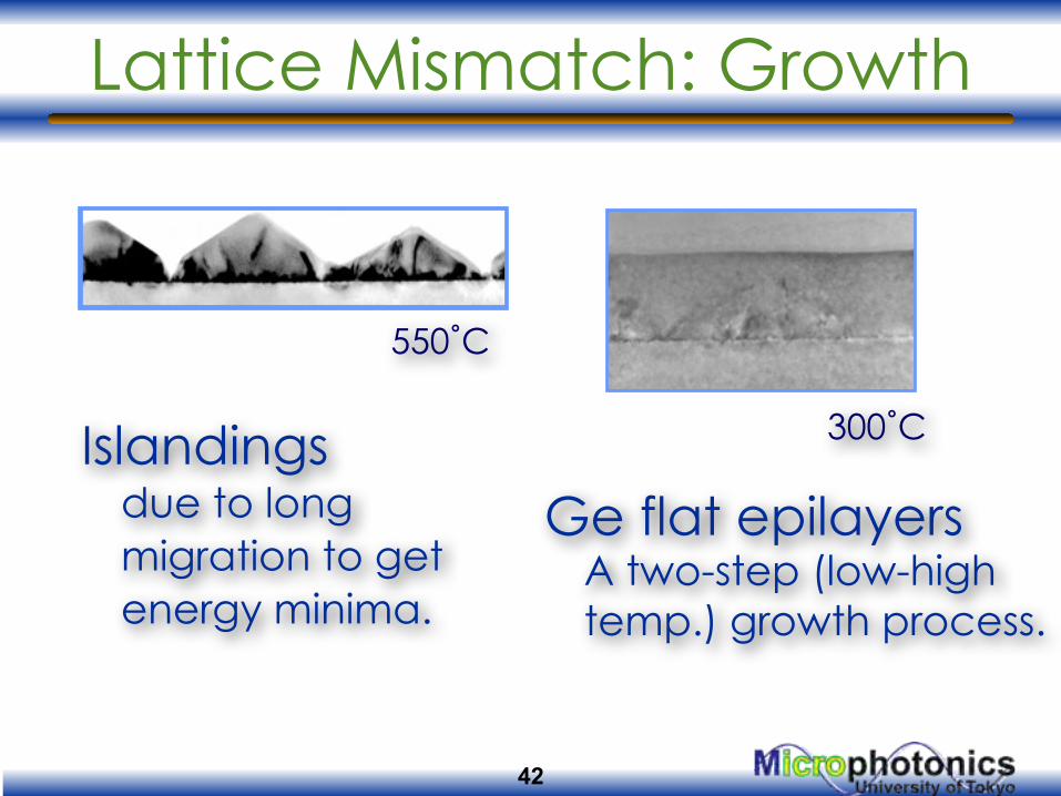
Lattice Mismatch: Growth
Ge flat epilayers A two-step (low-high temp.) growth process.
300˚C
550˚C
Islandingsdue to long migration to get energy minima.
42
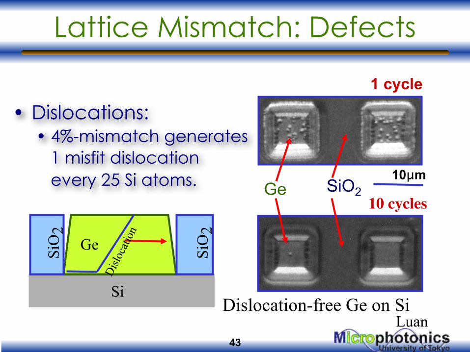
Lattice Mismatch: Defects
• Dislocations: • 4%-mismatch generates
1 misfit dislocation every 25 Si atoms.
Ge
Si
SiO
2
SiO
2
Dislo
catio
n
10μmGe SiO2
1 cycle
10 cycles
Dislocation-free Ge on SiLuan
43
44
Lattice Matching in Epitaxy
Lattice constant (A)
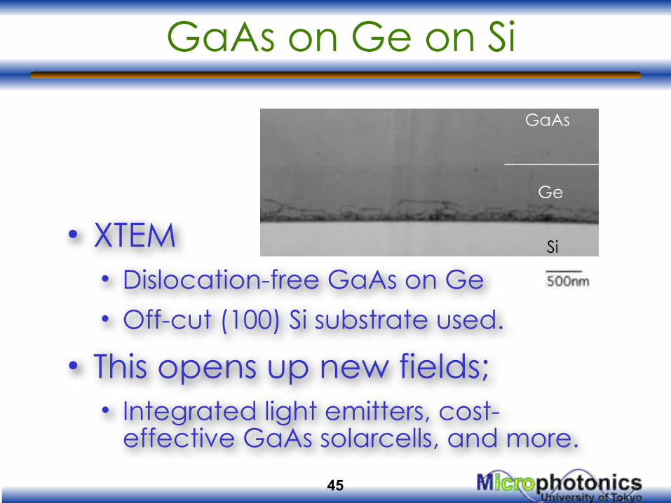
GaAs on Ge on Si
45
Si
Ge
GaAs
• This opens up new fields; • Integrated light emitters, cost-
effective GaAs solarcells, and more.
• XTEM• Dislocation-free GaAs on Ge
• Off-cut (100) Si substrate used.
Second Myth
• Ge works below 1550 nm to detect. • The typical communication wavelength
range is 1530-1620 nm (C+L band) because of Er doped fiber amp.
46
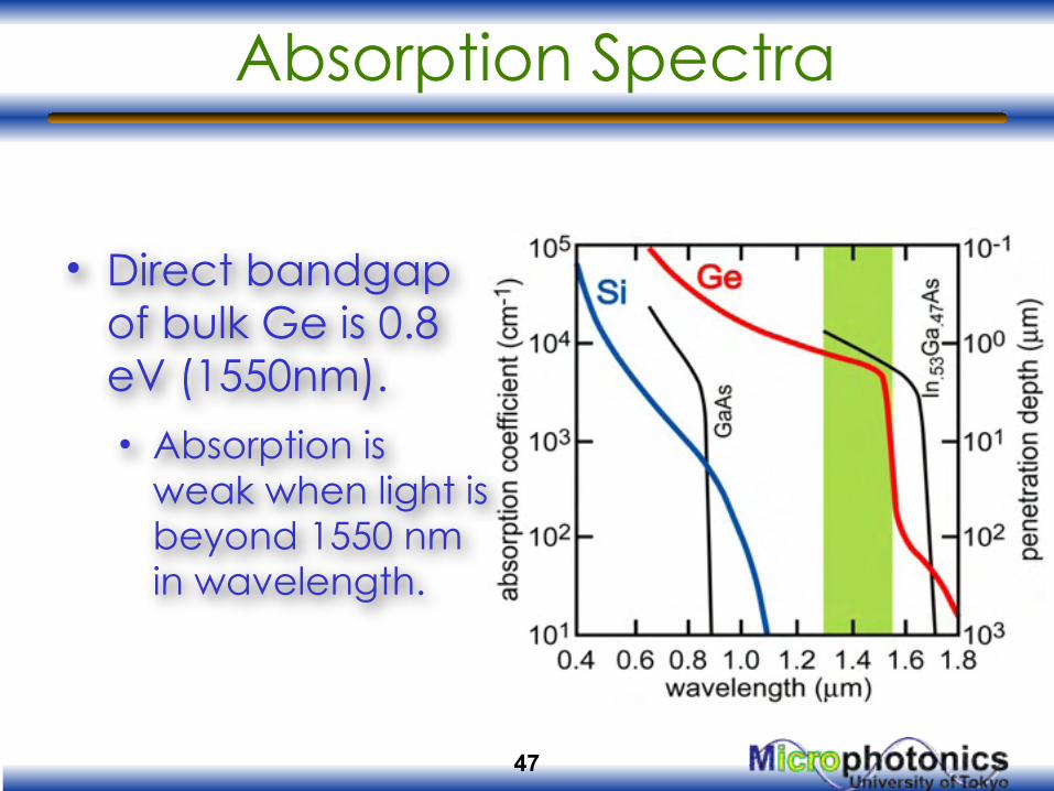
Absorption Spectra
47
• Direct bandgap of bulk Ge is 0.8 eV (1550nm).
• Absorption is weak when light is beyond 1550 nm in wavelength.
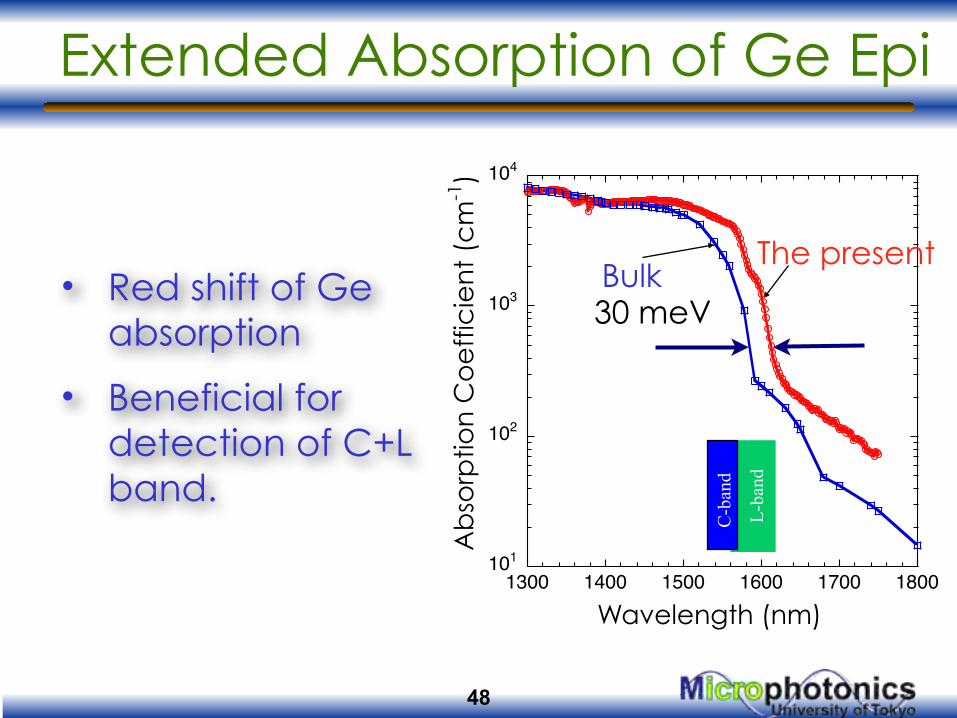
Extended Absorption of Ge Epi
• Red shift of Ge absorption
• Beneficial for detection of C+L band.
48
101
102
103
104
1300 1400 1500 1600 1700 1800
Wavelength (nm)
Ab
sorp
tion
Co
eff
icie
nt
(cm
-1)
The presentBulk
L-ba
nd
C-b
and
30 meV
49
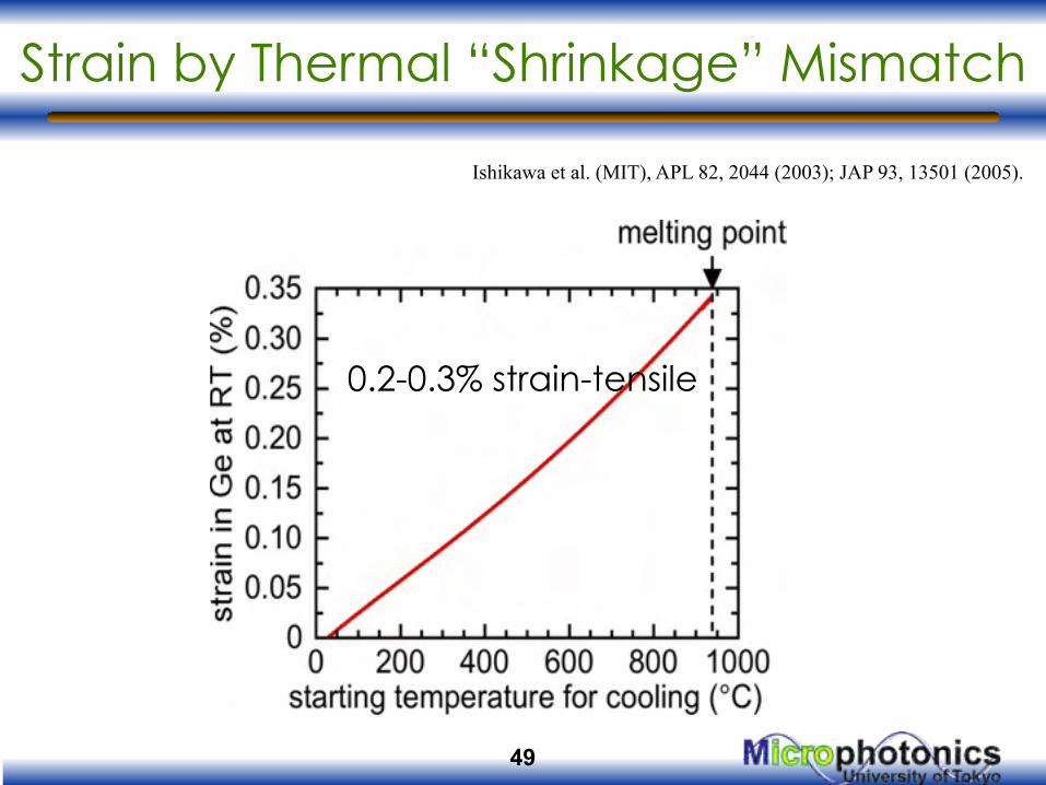
Thermal expansion coefficientGe > Si
Ishikawa et al. (MIT), APL 82, 2044 (2003); JAP 93, 13501 (2005).
Strain by Thermal “Shrinkage” Mismatch
0.2-0.3% strain-tensile
50
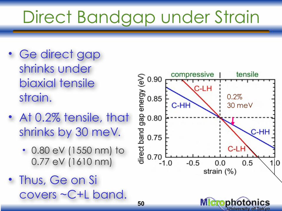
Direct Bandgap under Strain
0.2%30 meV
• Ge direct gap shrinks under biaxial tensile strain.
• At 0.2% tensile, that shrinks by 30 meV. • 0.80 eV (1550 nm) to
0.77 eV (1610 nm)
• Thus, Ge on Si covers ~C+L band.
Third Myth
• Laser needs direct transition type semiconductors. • Indirect semiconductors never lase.
51
52
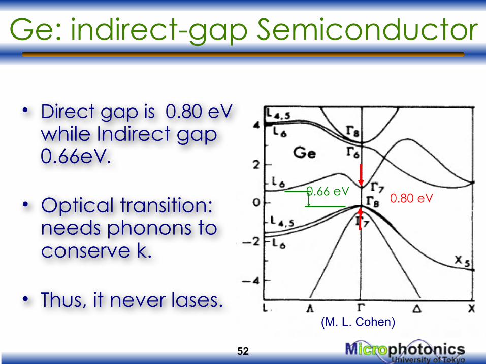
Ge: indirect-gap Semiconductor
0.80 eV0.66 eV
(M. L. Cohen)
• Direct gap is 0.80 eV while Indirect gap 0.66eV.
• Optical transition: needs phonons to conserve k.
• Thus, it never lases.
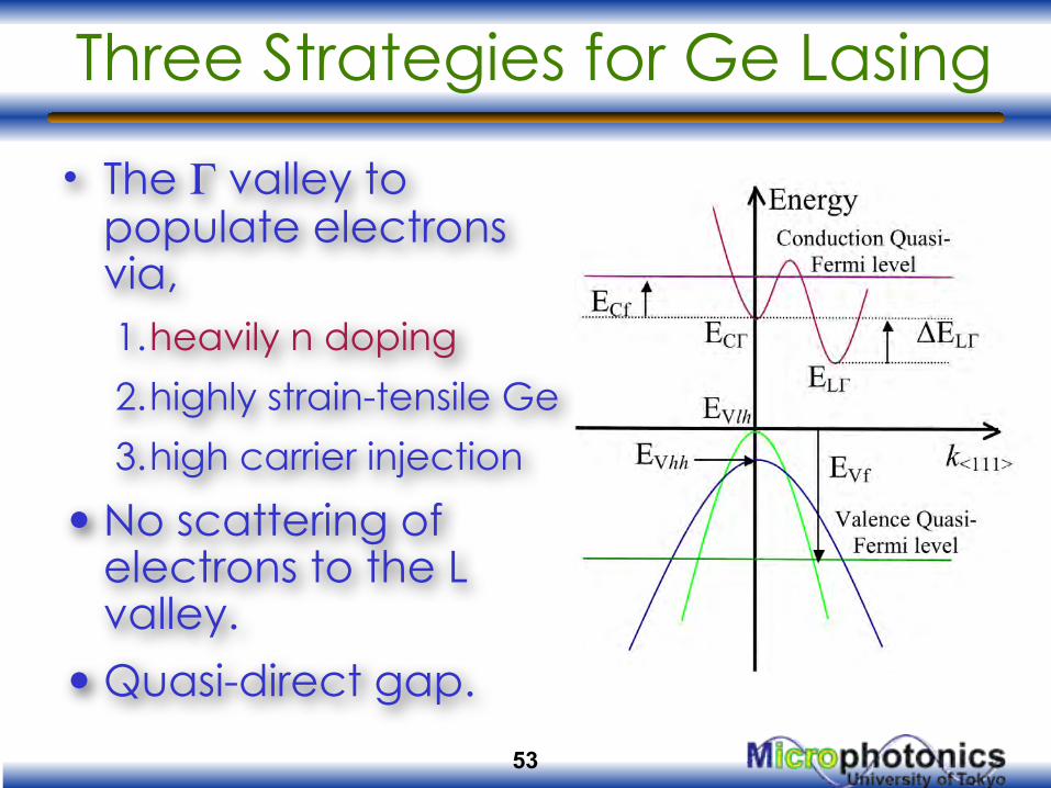
Three Strategies for Ge Lasing
• The Γ valley to populate electrons via, 1.heavily n doping
2.highly strain-tensile Ge
3.high carrier injection
• No scattering of electrons to the L valley.
• Quasi-direct gap.
53
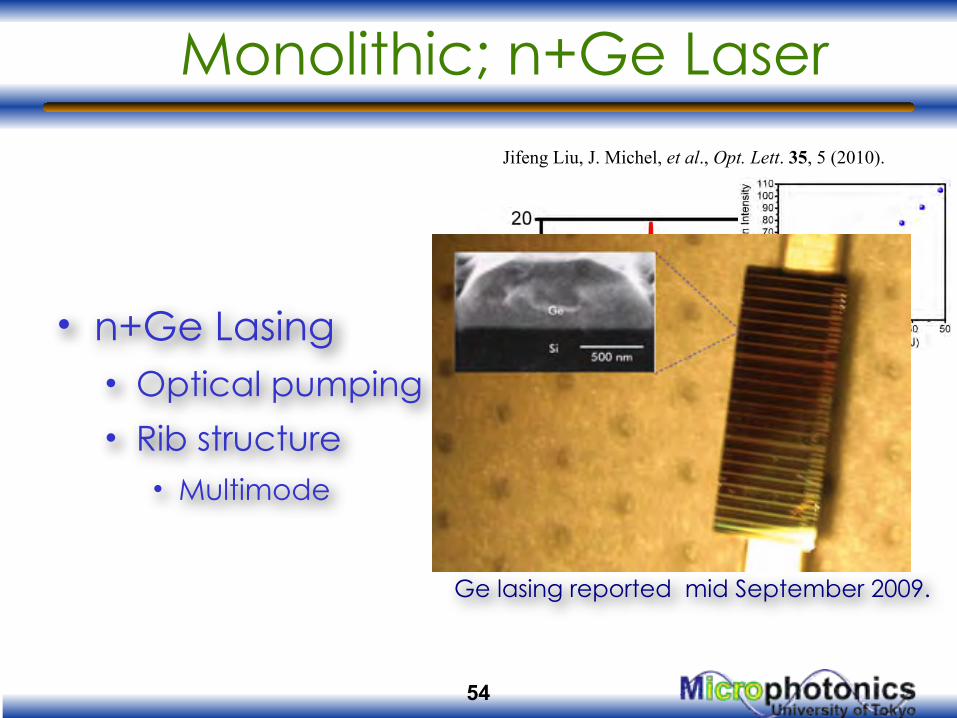
Monolithic; n+Ge Laser
54
Jifeng Liu, J. Michel, et al., Opt. Lett. 35, 5 (2010).
Ge lasing reported mid September 2009. !
• n+Ge Lasing• Optical pumping
• Rib structure• Multimode
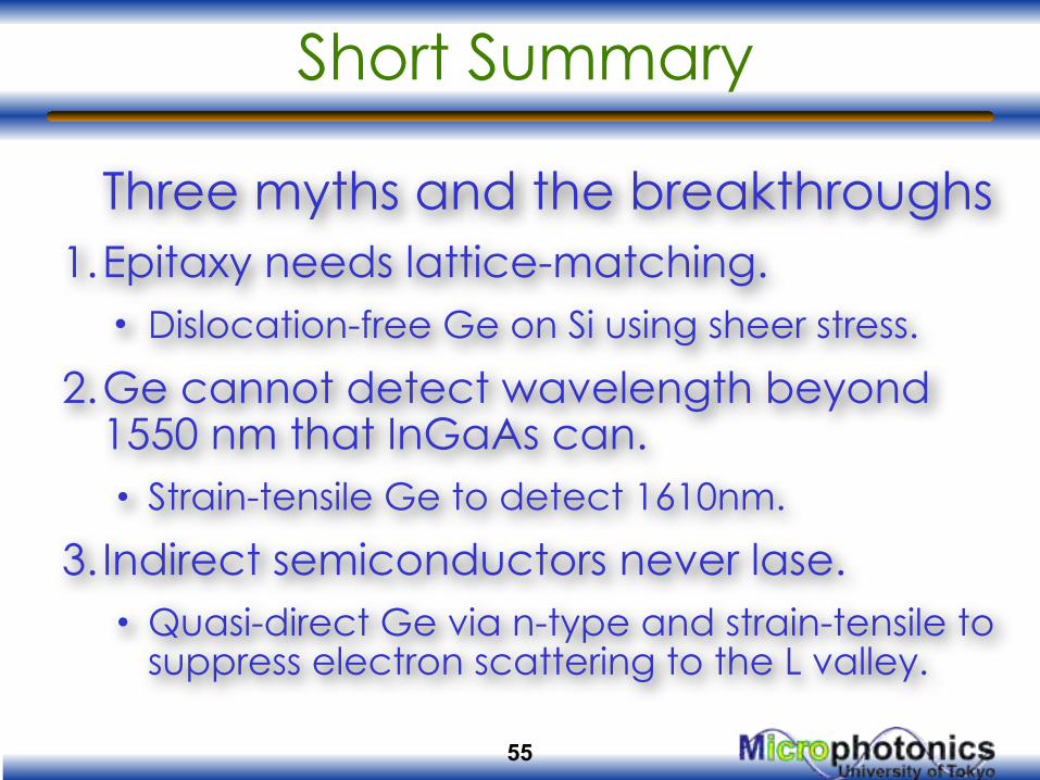
Short Summary
Three myths and the breakthroughs1.Epitaxy needs lattice-matching.
• Dislocation-free Ge on Si using sheer stress.
2.Ge cannot detect wavelength beyond 1550 nm that InGaAs can. • Strain-tensile Ge to detect 1610nm.
3. Indirect semiconductors never lase. • Quasi-direct Ge via n-type and strain-tensile to
suppress electron scattering to the L valley.
55
What we have learned
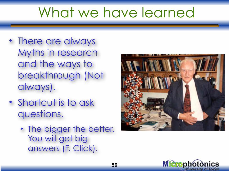
• There are always Myths in research and the ways to breakthrough (Not always).
• Shortcut is to ask questions.
• The bigger the better. You will get big answers (F. Click).
56
On-going Challenges
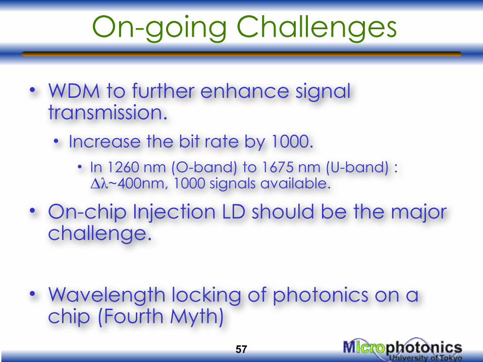
• WDM to further enhance signal transmission. • Increase the bit rate by 1000.
• In 1260 nm (O-band) to 1675 nm (U-band) : Δλ~400nm, 1000 signals available.
• On-chip Injection LD should be the major challenge.
• Wavelength locking of photonics on a chip (Fourth Myth)
57
carrier injection�
Carrier density from n-type doping (cm-3)�
Net
gai
n (c
m-1
)�
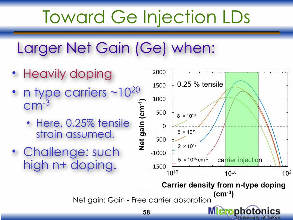
Toward Ge Injection LDs
• Heavily doping• n type carriers ~1020
cm-3
• Here, 0.25% tensile strain assumed.
• Challenge: such high n+ doping.
58
Net gain: Gain - Free carrier absorption
0.25 % tensile
Larger Net Gain (Ge) when:
5e18
1e192e19
in cm-3
5e19
Takinai, in this school
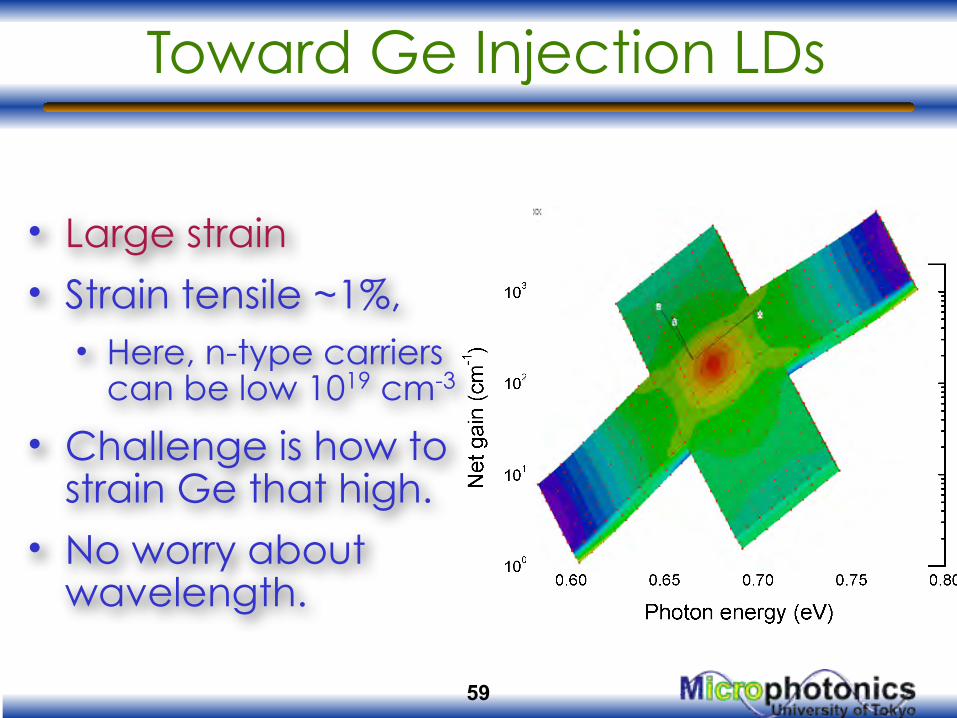
Toward Ge Injection LDs
59
• Large strain• Strain tensile ~1%,
• Here, n-type carriers can be low 1019 cm-3
• Challenge is how to strain Ge that high.
• No worry about wavelength.
The Fourth Myth (potential)
• LSIs and on-chip D(dense)WDM do not coexist under uncooled chip architecture (LSIs). • Thermal fluctuation on a chip malfunctions
DWDM because of wavelength fluctuation.
60
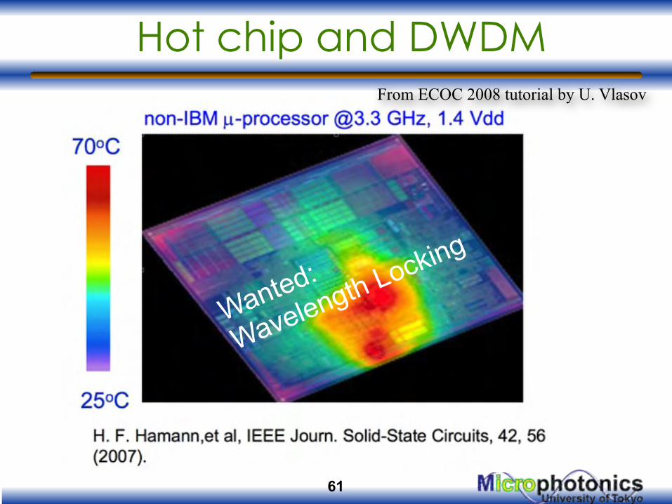
Hot chip and DWDM
61
From ECOC 2008 tutorial by U. Vlasov
Wanted:
Wavelength Locking
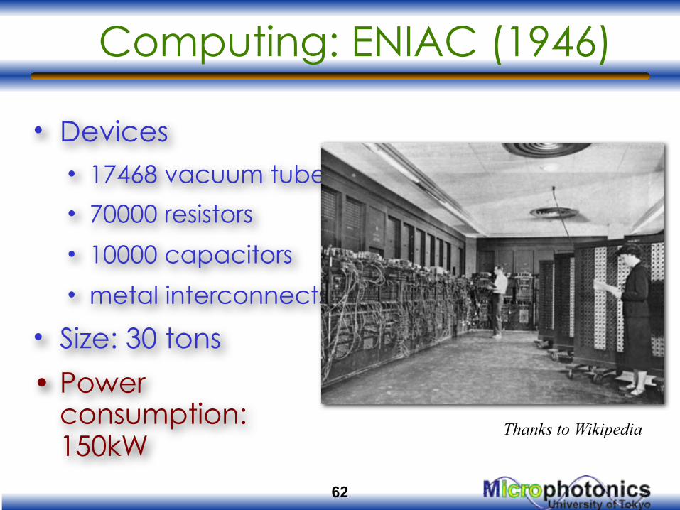
Computing: ENIAC (1946)
• Devices• 17468 vacuum tubes
• 70000 resistors
• 10000 capacitors
• metal interconnects
• Size: 30 tons
• Power consumption: 150kW
Thanks to Wikipedia
62
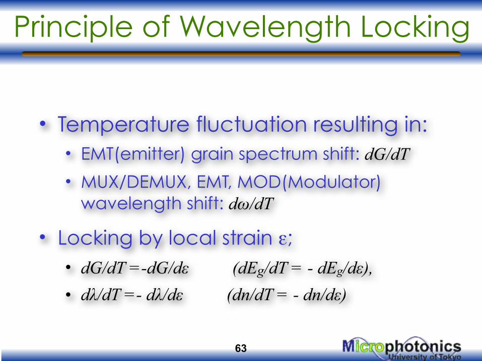
Principle of Wavelength Locking
• Temperature fluctuation resulting in:• EMT(emitter) grain spectrum shift: dG/dT
• MUX/DEMUX, EMT, MOD(Modulator) wavelength shift: dω/dT
• Locking by local strain ε; • dG/dT =-dG/dε (dEg/dT = - dEg/dε), • dλ/dT =- dλ/dε (dn/dT = - dn/dε)
63
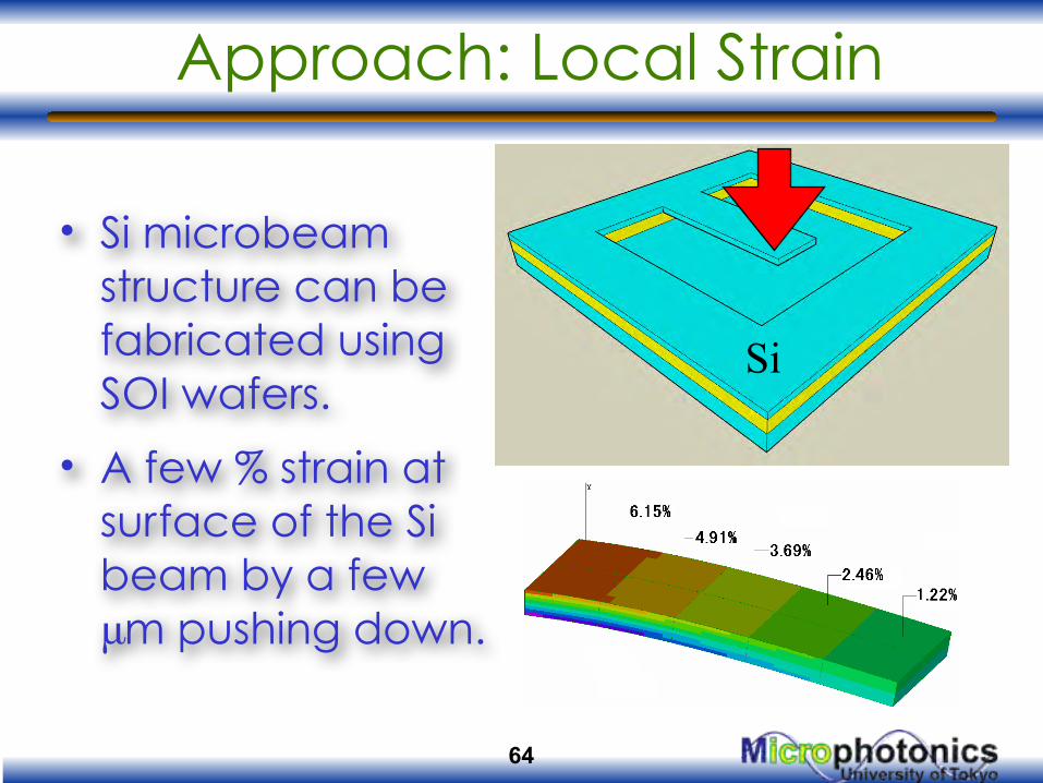
• Si microbeam structure can be fabricated using SOI wafers.
• A few % strain at surface of the Si beam by a few μm pushing down.
Approach: Local Strain
64
Si
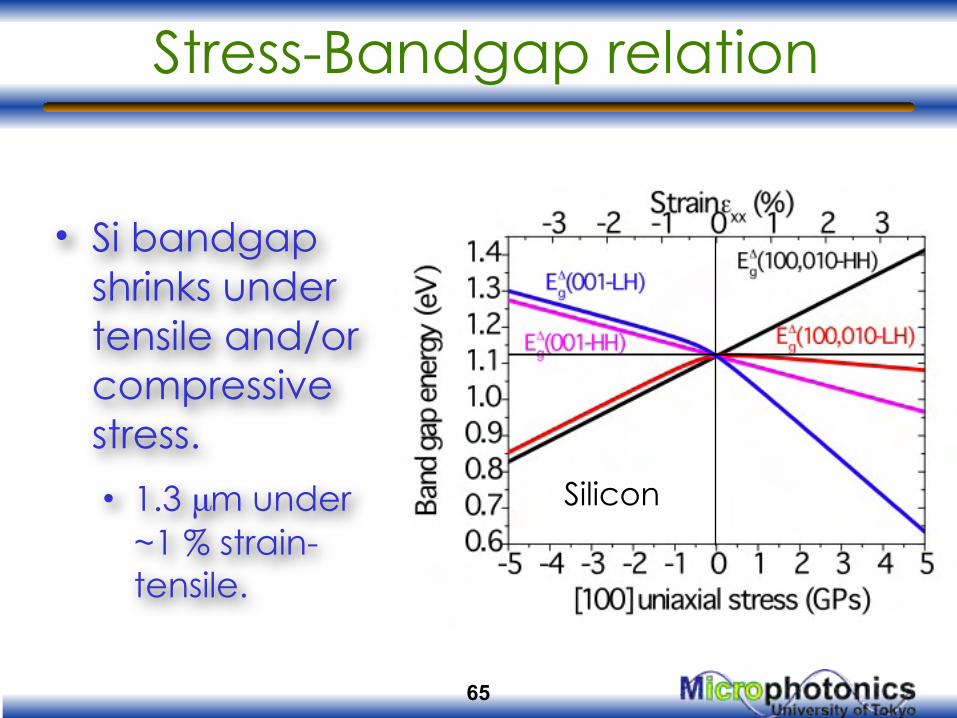
Stress-Bandgap relation
• Si bandgap shrinks under tensile and/or compressive stress.
• 1.3 μm under ~1 % strain-tensile.
65
Silicon
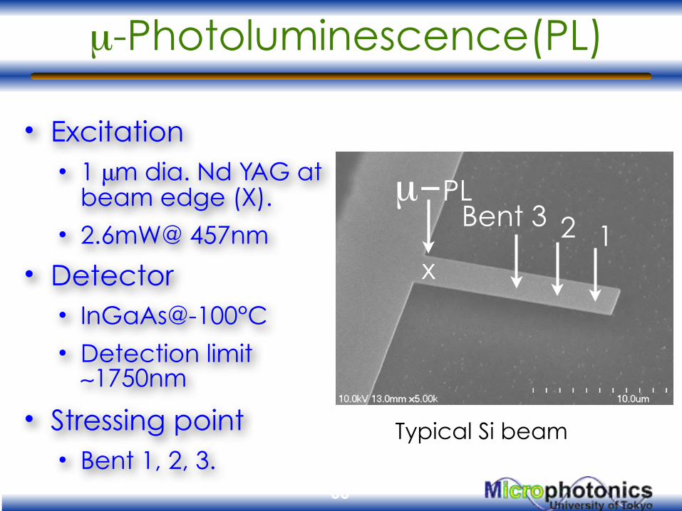
µ-Photoluminescence(PL)
• Excitation• 1 μm dia. Nd YAG at
beam edge (X).
• 2.6mW@ 457nm
• Detector• InGaAs@-100°C
• Detection limit ∼1750nm
• Stressing point• Bent 1, 2, 3.
66
Typical Si beam
Bent 3 2 1x
µ-PL
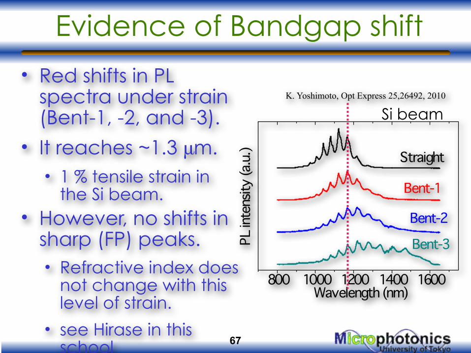
Evidence of Bandgap shift
• Red shifts in PL spectra under strain (Bent-1, -2, and -3).
• It reaches ~1.3 μm. • 1 % tensile strain in
the Si beam.
67
K. Yoshimoto, Opt Express 25,26492, 2010
Si beam
• However, no shifts in sharp (FP) peaks. • Refractive index does
not change with this level of strain.
• see Hirase in this school
Horie, in this school
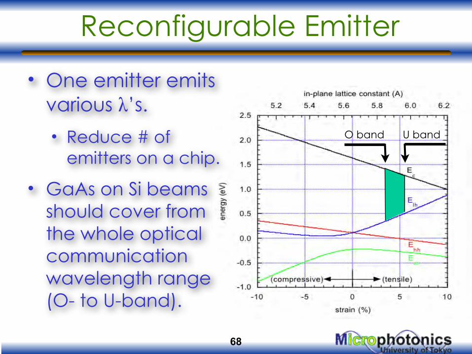
Reconfigurable Emitter
68
O band U band
• One emitter emits various λ’s. • Reduce # of
emitters on a chip.
• GaAs on Si beams should cover from the whole optical communication wavelength range (O- to U-band).
Horie, in this school
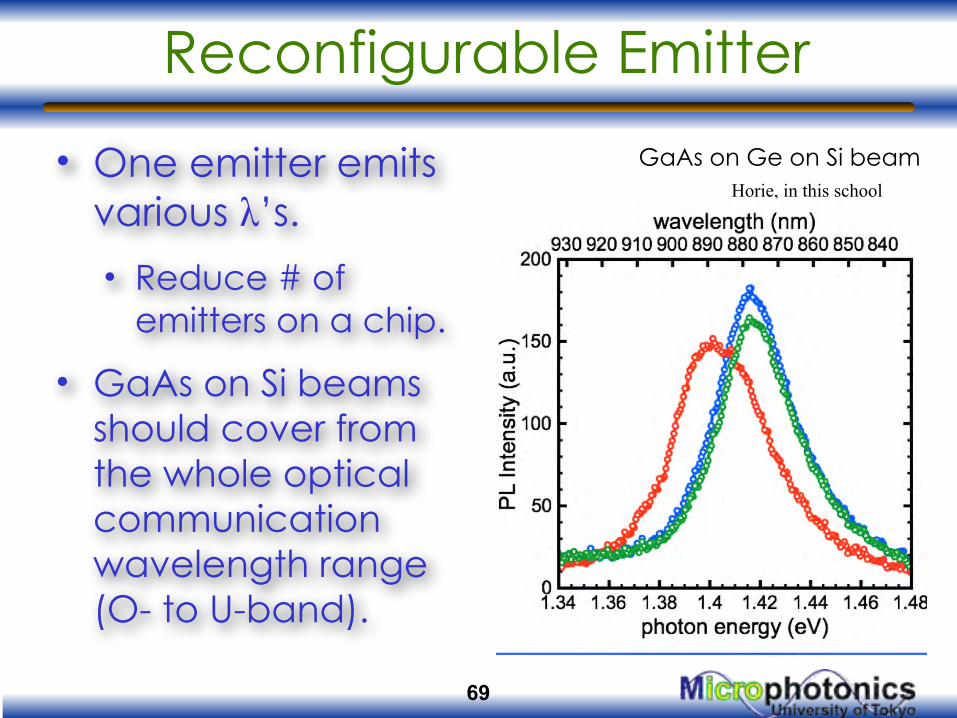
Reconfigurable Emitter
69
GaAs on Ge on Si beam• One emitter emits various λ’s. • Reduce # of
emitters on a chip.
• GaAs on Si beams should cover from the whole optical communication wavelength range (O- to U-band).
Summary
• The three myths and the breakthroughs in early Si photonics reviewed
• Challenges of WDM implementation in Si electronics reviewed.• Wavelength locking via strained Si, Ge, and
GaAs.
• Demands on on-chip WDM: • Injection Ge laser: by n+ and strain+
• Reconfigurable(Tunable) emitter: GaAs on Ge on Si beam.
70