Embed Size (px)
Citation preview

AJAMANGALA UNIVERSITY of TECHNOLOGY SRIVIJAYAMUTSV, ELECTRONIC ENGINEERINGR
Bipolar Amplifiers
อาจารย์ผู้สอน : อภริักษ์ เสือเดช
Email : [email protected]
Website : www.suadet.yolasite.com
2
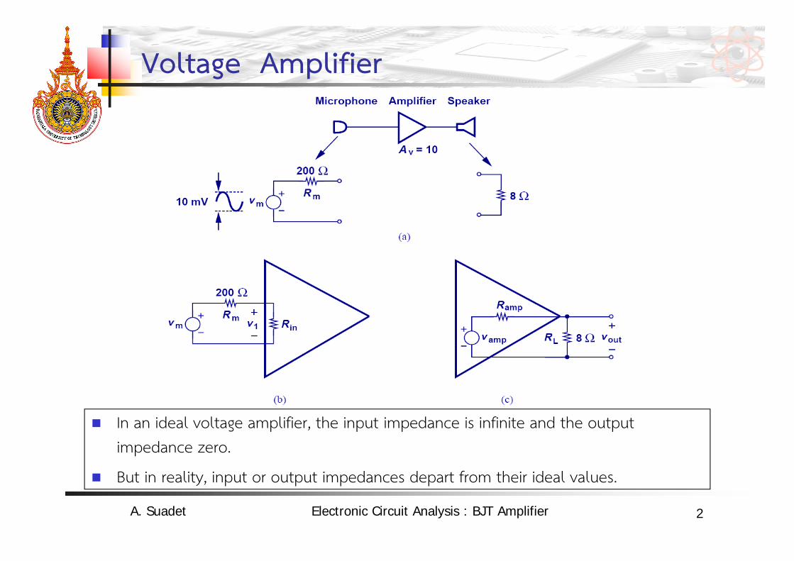
Voltage Amplifier
In an ideal voltage amplifier, the input impedance is infinite and the output impedance zero.
But in reality, input or output impedances depart from their ideal values.
A. Suadet Electronic Circuit Analysis : BJT Amplifier
3
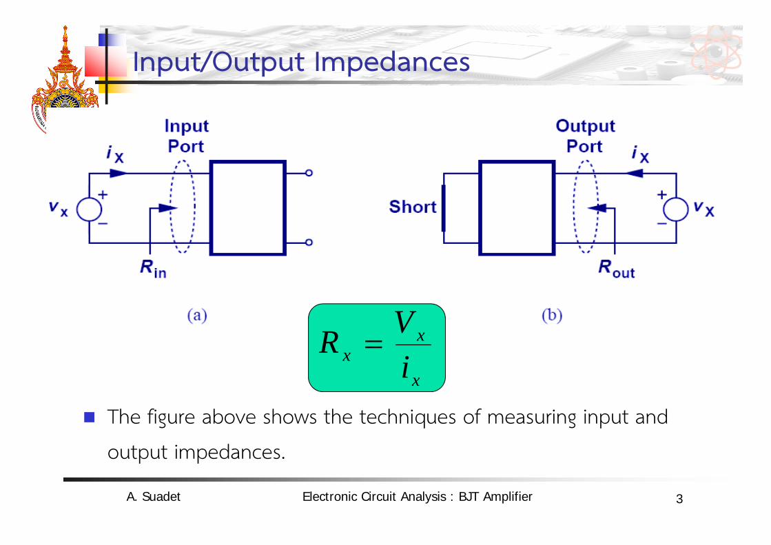
Input/Output Impedances
The figure above shows the techniques of measuring input and
output impedances.
x
xx i
VR
A. Suadet Electronic Circuit Analysis : BJT Amplifier
4
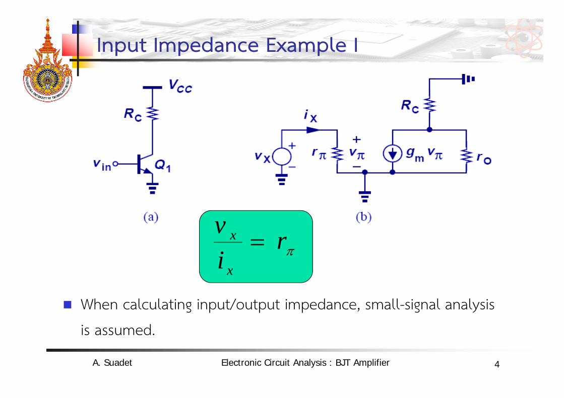
Input Impedance Example I
When calculating input/output impedance, small-signal analysis
is assumed.
riv
x
x
A. Suadet Electronic Circuit Analysis : BJT Amplifier
5
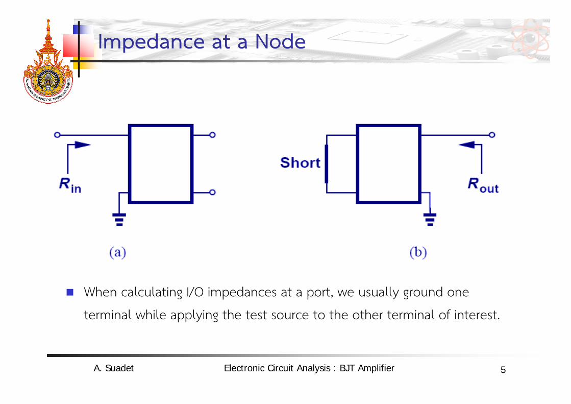
Impedance at a Node
When calculating I/O impedances at a port, we usually ground one
terminal while applying the test source to the other terminal of interest.
A. Suadet Electronic Circuit Analysis : BJT Amplifier
6
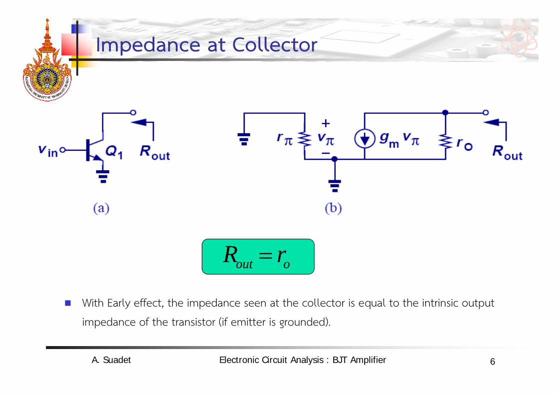
Impedance at Collector
With Early effect, the impedance seen at the collector is equal to the intrinsic output
impedance of the transistor (if emitter is grounded).
oout rR
A. Suadet Electronic Circuit Analysis : BJT Amplifier
7
Impedance at Emitter
The impedance seen at the emitter of a transistor is approximately equal to one over its transconductance (if the base is grounded).
)(
1
11
A
mout
mx
x
Vg
R
rgi
v
A. Suadet Electronic Circuit Analysis : BJT Amplifier
8
Three Master Rules of Transistor Impedances
Rule # 1: looking into the base, the impedance is r if emitter is (ac) grounded.
Rule # 2: looking into the collector, the impedance is ro if emitter is (ac) grounded.
Rule # 3: looking into the emitter, the impedance is 1/gm if base is (ac) grounded and Early effect is neglected.
A. Suadet Electronic Circuit Analysis : BJT Amplifier
9
Biasing of BJT
Transistors and circuits must be biased because (1) transistors
must operate in the active region, (2) their small-signal
parameters depend on the bias conditions.
A. Suadet Electronic Circuit Analysis : BJT Amplifier
10
DC Analysis vs. Small-Signal Analysis
First, DC analysis is performed to determine operating point and obtain small-signal parameters.
Second, sources are set to zero and small-signal model is used.
A. Suadet Electronic Circuit Analysis : BJT Amplifier

11
Notation Simplification
Hereafter, the battery that supplies power to the circuit is replaced by a horizontal bar labeled Vcc, and input signal is simplified as one node called Vin.
A. Suadet Electronic Circuit Analysis : BJT Amplifier
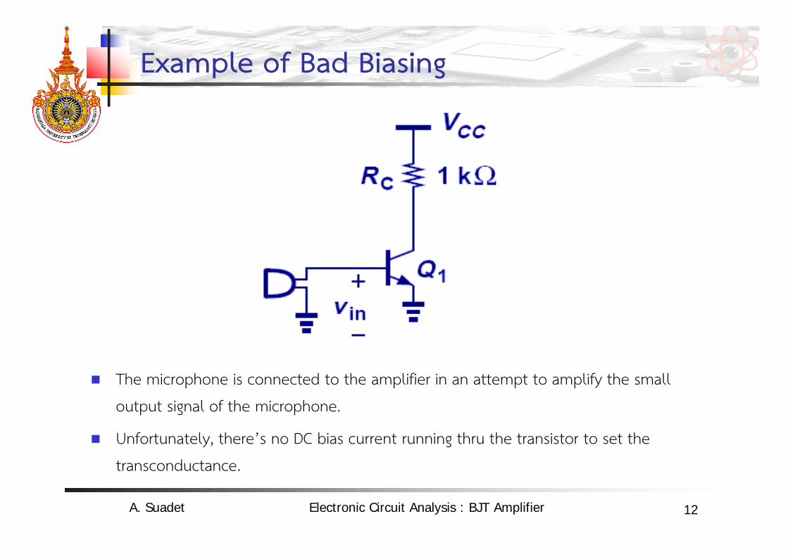
12
Example of Bad Biasing
The microphone is connected to the amplifier in an attempt to amplify the small
output signal of the microphone.
Unfortunately, there’s no DC bias current running thru the transistor to set the
transconductance.
A. Suadet Electronic Circuit Analysis : BJT Amplifier
13
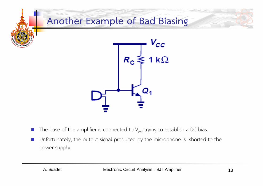
Another Example of Bad Biasing
The base of the amplifier is connected to Vcc, trying to establish a DC bias.
Unfortunately, the output signal produced by the microphone is shorted to the power supply.
A. Suadet Electronic Circuit Analysis : BJT Amplifier
14
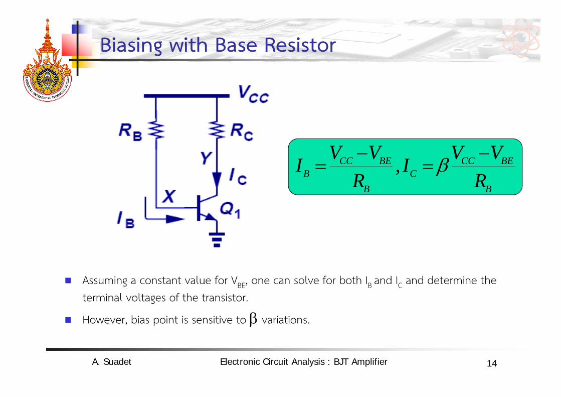
Biasing with Base Resistor
Assuming a constant value for VBE, one can solve for both IB and IC and determine the terminal voltages of the transistor.
However, bias point is sensitive to variations.
B
BECCC
B
BECCB R
VVIR
VVI
,
A. Suadet Electronic Circuit Analysis : BJT Amplifier
15
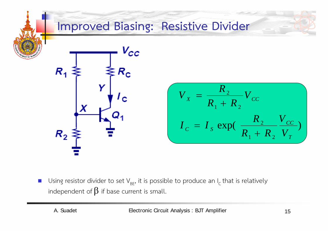
Improved Biasing: Resistive Divider
Using resistor divider to set VBE, it is possible to produce an IC that is relatively independent of if base current is small.
)exp(21
2
21
2
T
CCSC
CCX
VV
RRRII
VRR
RV
A. Suadet Electronic Circuit Analysis : BJT Amplifier
16
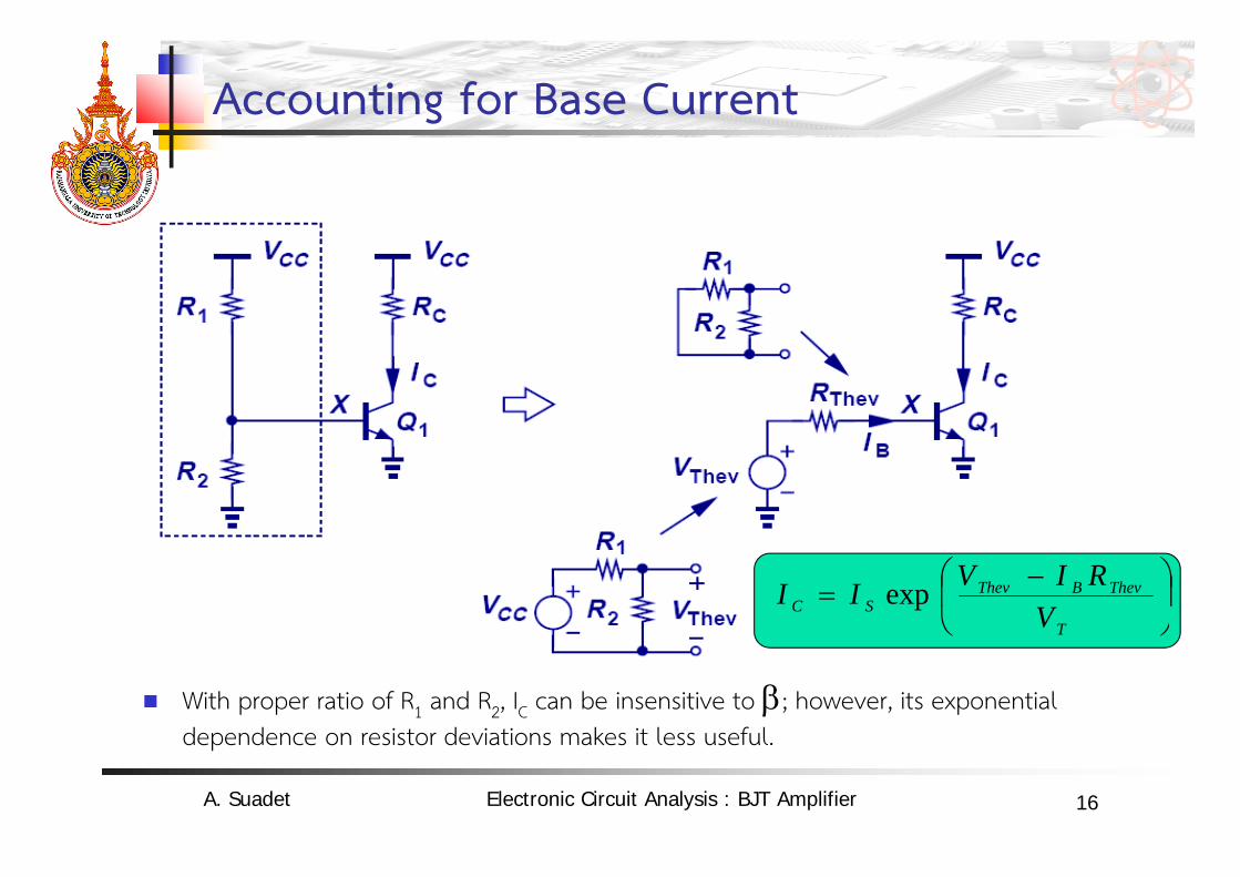
Accounting for Base Current
With proper ratio of R1 and R2, IC can be insensitive to ; however, its exponential dependence on resistor deviations makes it less useful.
T
ThevBThevSC V
RIVII exp
A. Suadet Electronic Circuit Analysis : BJT Amplifier
17
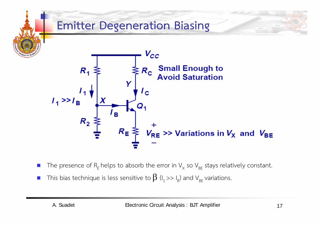
Emitter Degeneration Biasing
The presence of RE helps to absorb the error in VX so VBE stays relatively constant.
This bias technique is less sensitive to (I1 >> IB) and VBE variations.
A. Suadet Electronic Circuit Analysis : BJT Amplifier
18
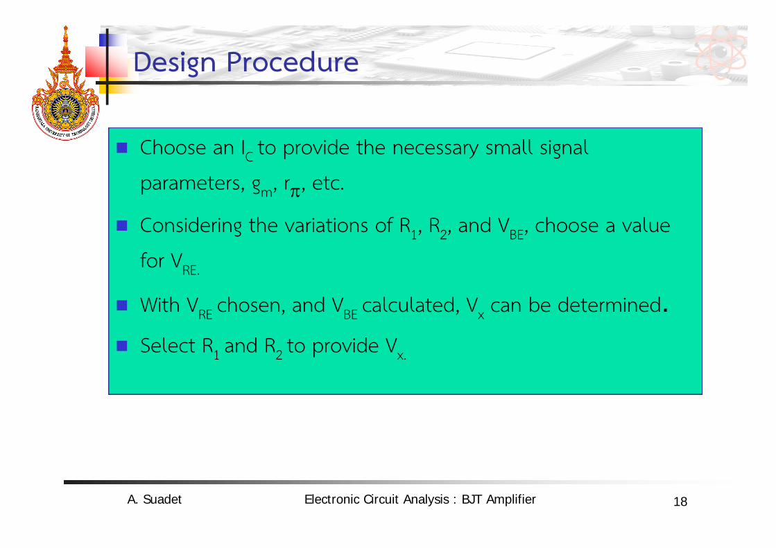
Design Procedure
Choose an IC to provide the necessary small signal
parameters, gm, r, etc.
Considering the variations of R1, R2, and VBE, choose a value
for VRE.
With VRE chosen, and VBE calculated, Vx can be determined. Select R1 and R2 to provide Vx.
A. Suadet Electronic Circuit Analysis : BJT Amplifier
19
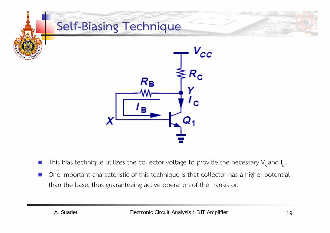
Self-Biasing Technique
This bias technique utilizes the collector voltage to provide the necessary Vx and IB.
One important characteristic of this technique is that collector has a higher potential than the base, thus guaranteeing active operation of the transistor.
A. Suadet Electronic Circuit Analysis : BJT Amplifier
20
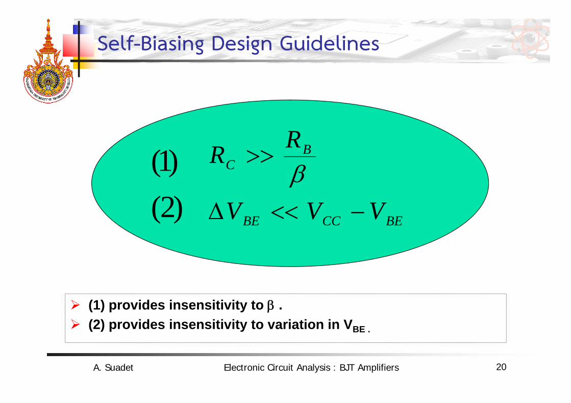
Self-Biasing Design Guidelines
(1) provides insensitivity to . (2) provides insensitivity to variation in VBE .
BECCBE
BC
VVV
RR
)2()1(
A. Suadet Electronic Circuit Analysis : BJT Amplifiers

21
Summary of Biasing Techniques
A. Suadet Electronic Circuit Analysis : BJT Amplifier
22
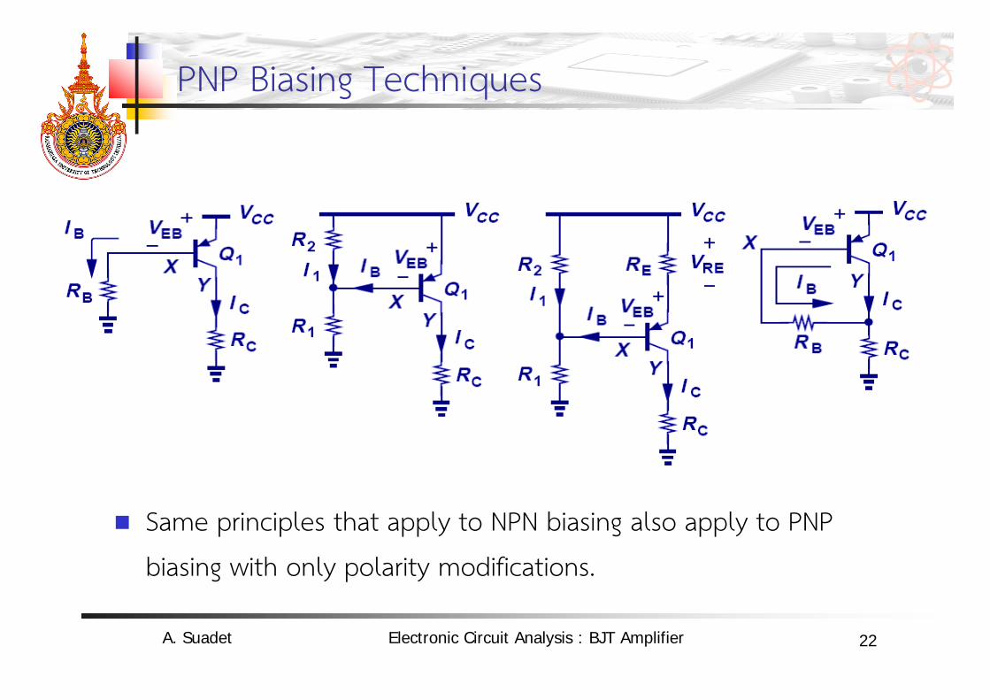
PNP Biasing Techniques
Same principles that apply to NPN biasing also apply to PNP
biasing with only polarity modifications.
A. Suadet Electronic Circuit Analysis : BJT Amplifier
23
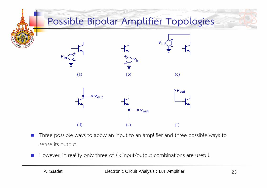
Possible Bipolar Amplifier Topologies
Three possible ways to apply an input to an amplifier and three possible ways to
sense its output.
However, in reality only three of six input/output combinations are useful.
A. Suadet Electronic Circuit Analysis : BJT Amplifier
24
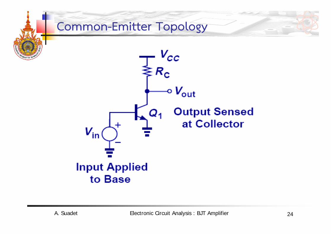
Common-Emitter Topology
A. Suadet Electronic Circuit Analysis : BJT Amplifier
25
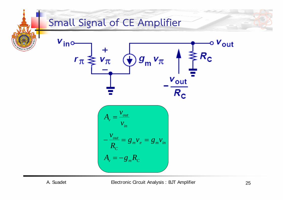
Small Signal of CE Amplifier
Cmv
inmmC
out
in
outv
RgA
vgvgRv
vvA
A. Suadet Electronic Circuit Analysis : BJT Amplifier
26
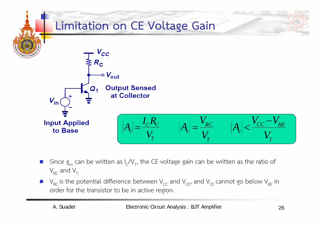
Limitation on CE Voltage Gain
Since gm can be written as IC/VT, the CE voltage gain can be written as the ratio of VRC and VT.
VRC is the potential difference between VCC and VCE, and VCE cannot go below VBE in order for the transistor to be in active region.
T
CCv V
RIA T
RCv V
VA T
BECCv V
VVA
A. Suadet Electronic Circuit Analysis : BJT Amplifier
27
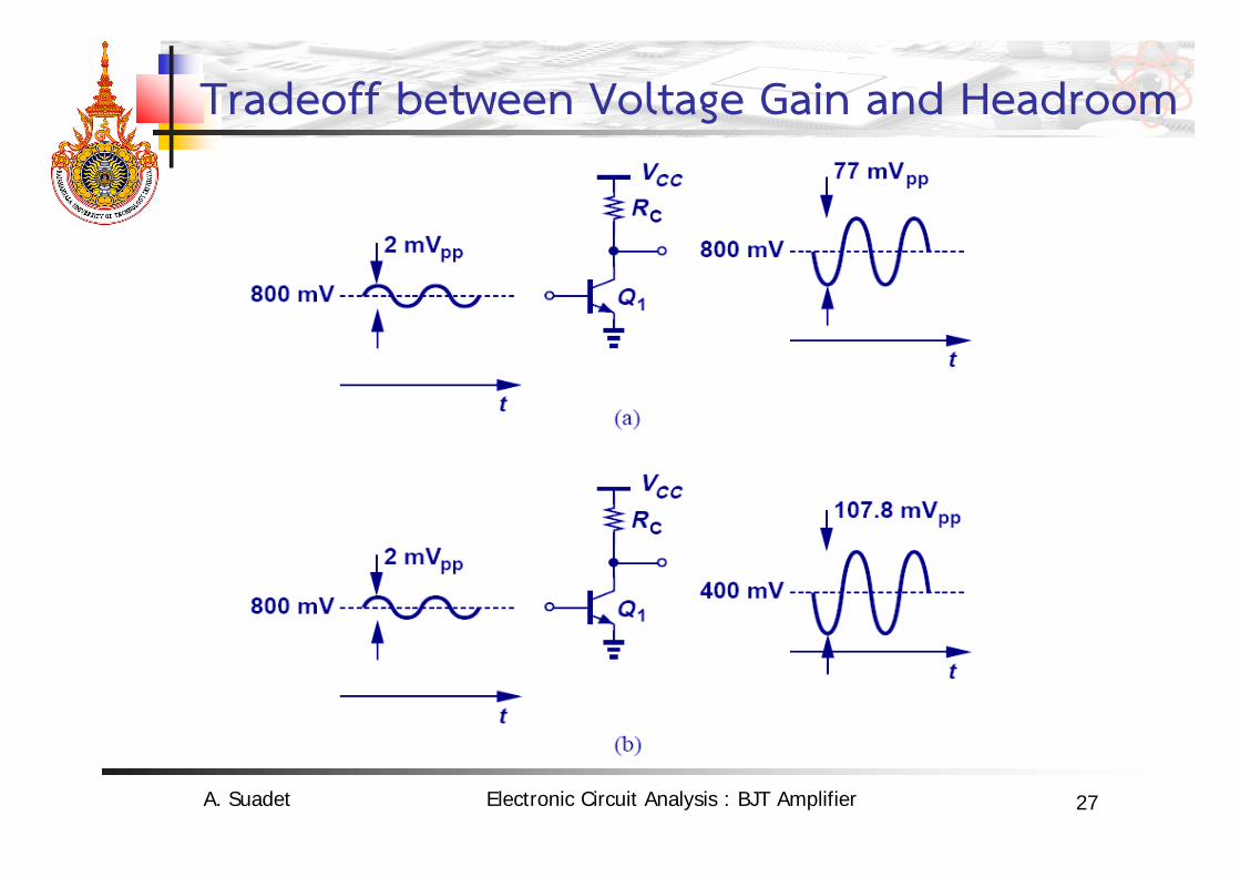
Tradeoff between Voltage Gain and Headroom
A. Suadet Electronic Circuit Analysis : BJT Amplifier
28
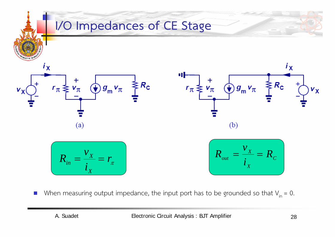
I/O Impedances of CE Stage
When measuring output impedance, the input port has to be grounded so that Vin = 0.
rivR
X
Xin C
X
Xout R
ivR
A. Suadet Electronic Circuit Analysis : BJT Amplifier
29
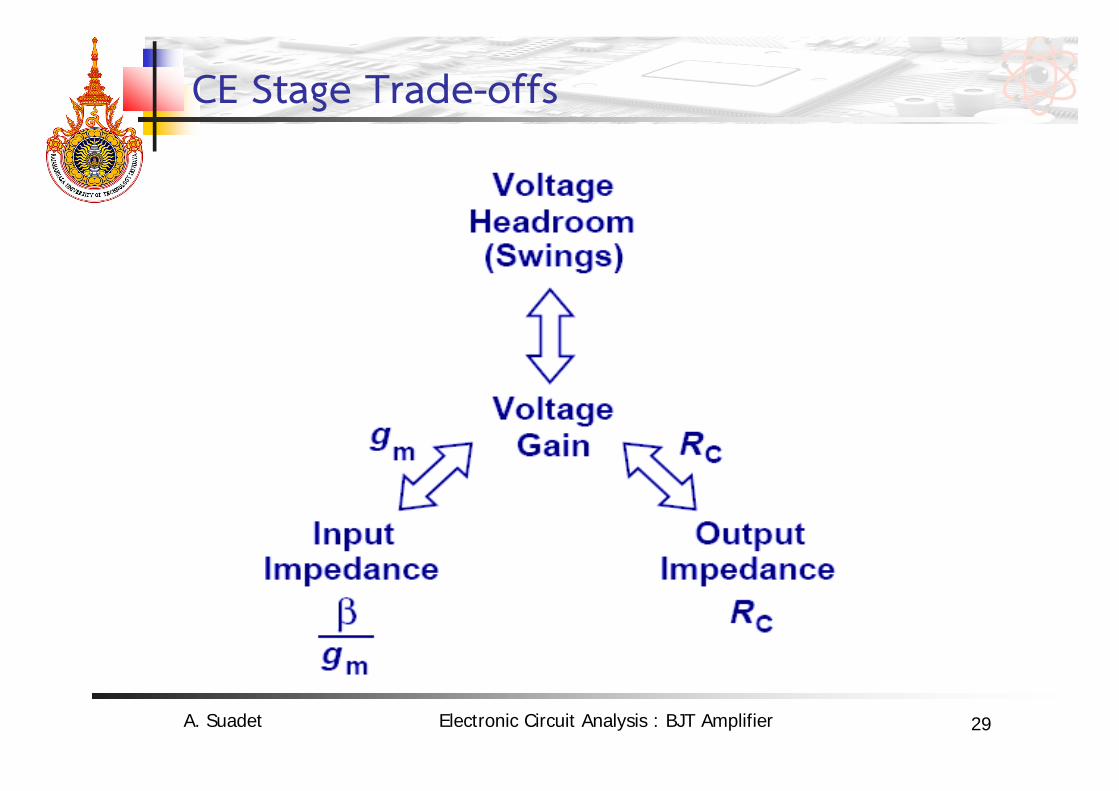
CE Stage Trade-offs
A. Suadet Electronic Circuit Analysis : BJT Amplifier
30
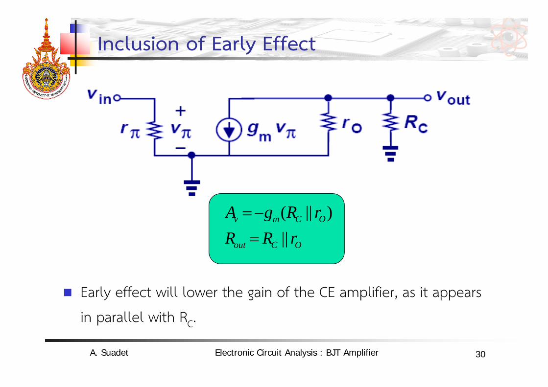
Inclusion of Early Effect
Early effect will lower the gain of the CE amplifier, as it appears
in parallel with RC.
OCout
OCmv
rRRrRgA
||)||(
A. Suadet Electronic Circuit Analysis : BJT Amplifier
31
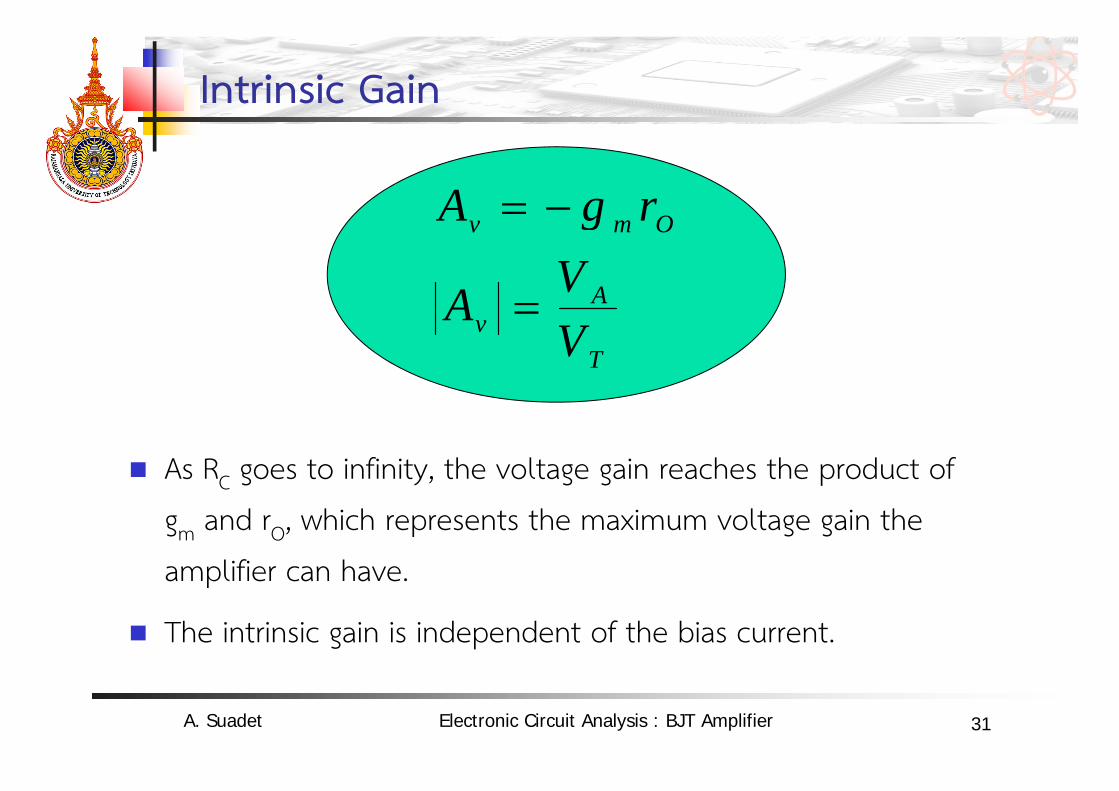
Intrinsic Gain
As RC goes to infinity, the voltage gain reaches the product of
gm and rO, which represents the maximum voltage gain the
amplifier can have.
The intrinsic gain is independent of the bias current.
T
Av
Omv
VVA
rgA
A. Suadet Electronic Circuit Analysis : BJT Amplifier
32
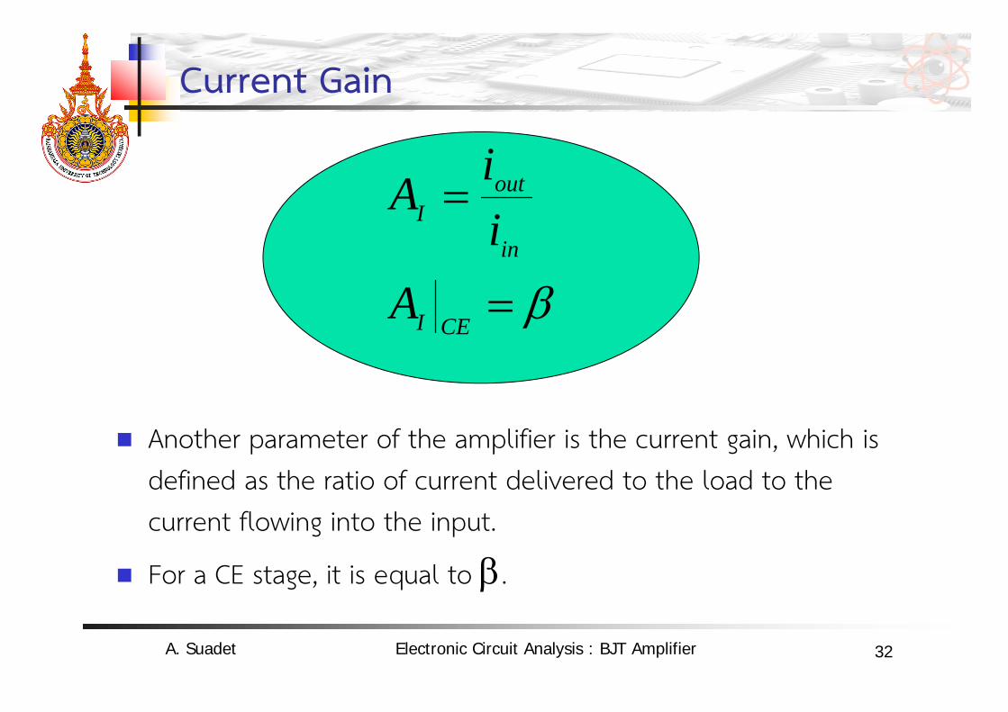
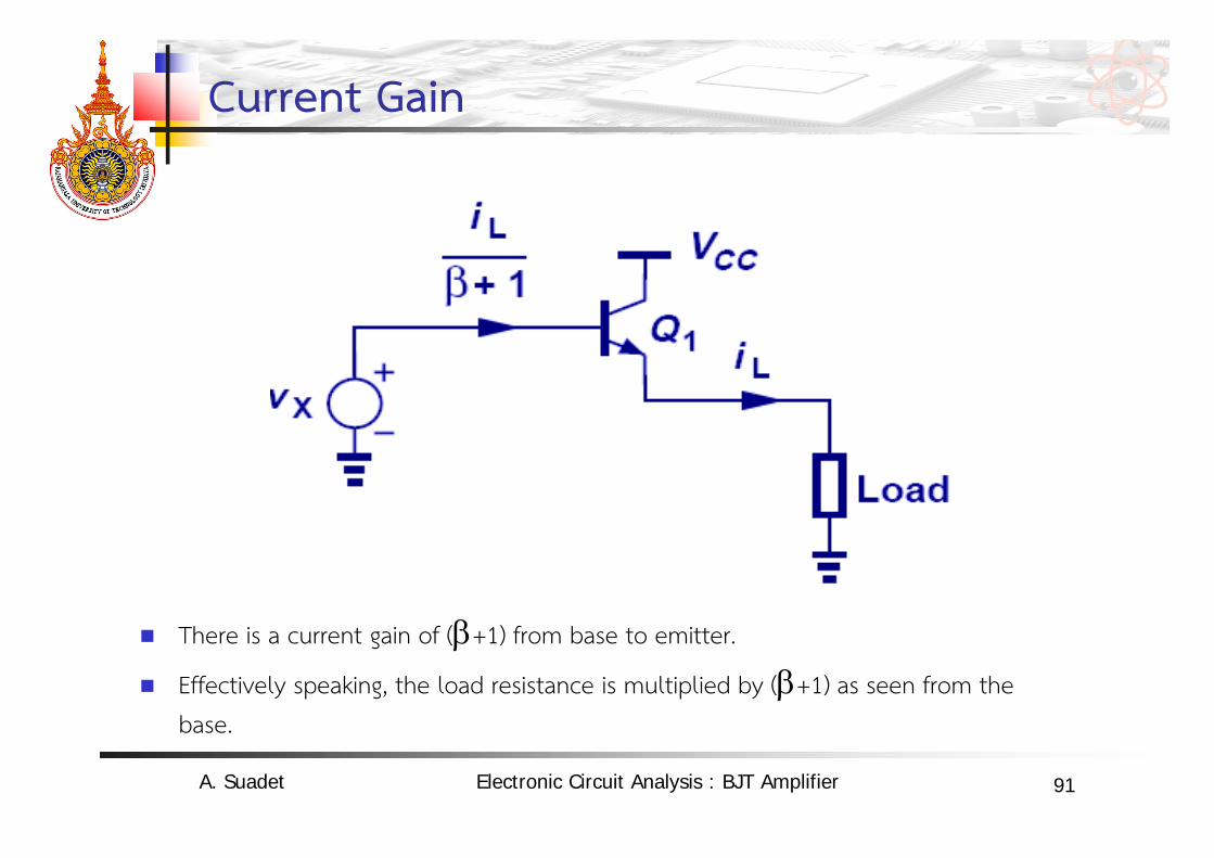
Current Gain
Another parameter of the amplifier is the current gain, which is defined as the ratio of current delivered to the load to the current flowing into the input.
For a CE stage, it is equal to .
CEI
in
outI
AiiA
A. Suadet Electronic Circuit Analysis : BJT Amplifier
33
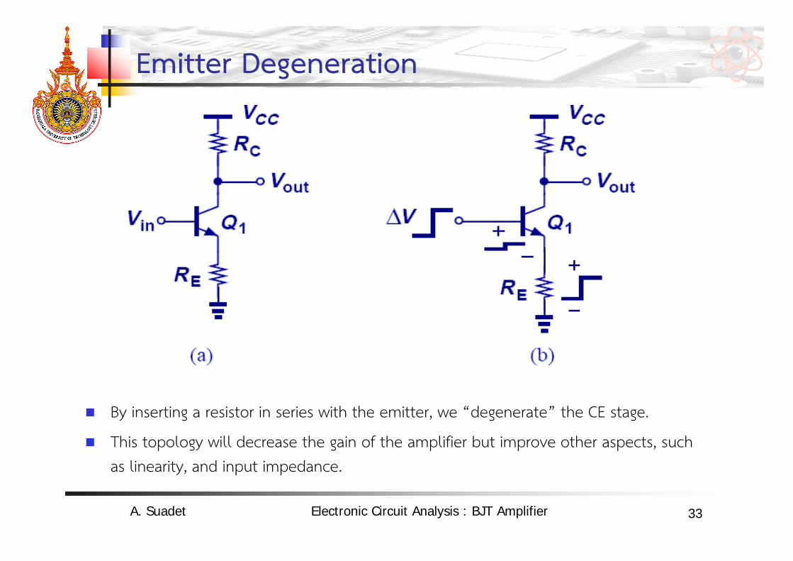
Emitter Degeneration
By inserting a resistor in series with the emitter, we “degenerate” the CE stage.
This topology will decrease the gain of the amplifier but improve other aspects, such as linearity, and input impedance.
A. Suadet Electronic Circuit Analysis : BJT Amplifier
34
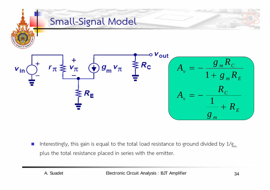
Small-Signal Model
Interestingly, this gain is equal to the total load resistance to ground divided by 1/gm
plus the total resistance placed in series with the emitter.
Em
Cv
Em
Cmv
Rg
RA
RgRgA
1
1
A. Suadet Electronic Circuit Analysis : BJT Amplifier
35
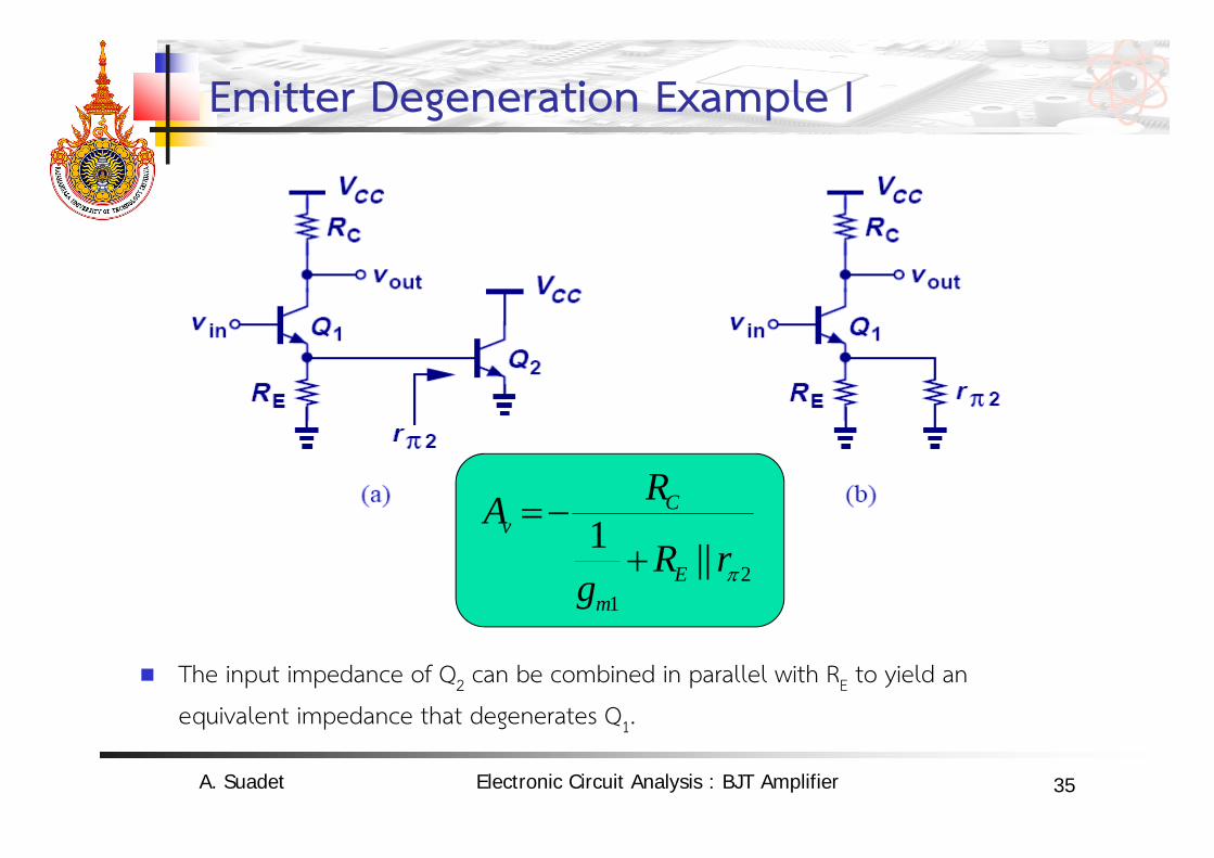
Emitter Degeneration Example I
The input impedance of Q2 can be combined in parallel with RE to yield an
equivalent impedance that degenerates Q1.
21
||1rR
g
RAE
m
Cv
A. Suadet Electronic Circuit Analysis : BJT Amplifier
36
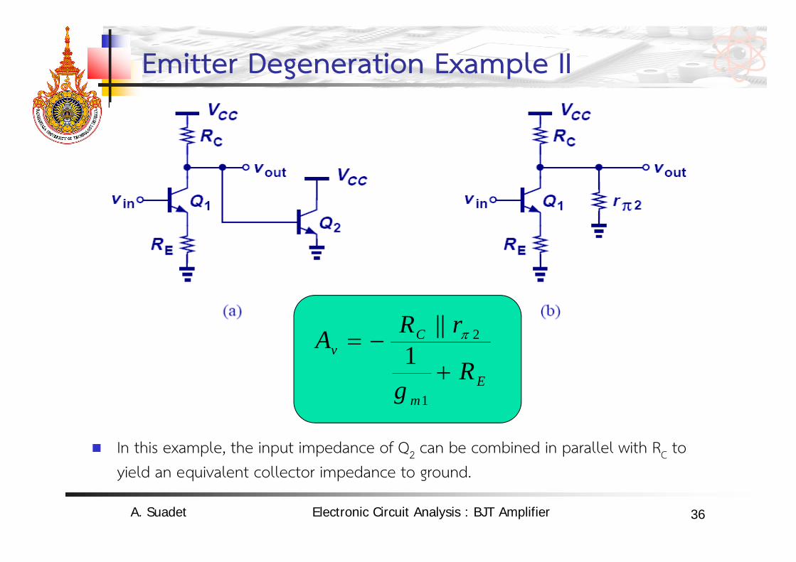
Emitter Degeneration Example II
In this example, the input impedance of Q2 can be combined in parallel with RC to yield an equivalent collector impedance to ground.
Em
Cv
Rg
rRA
1
2
1||
A. Suadet Electronic Circuit Analysis : BJT Amplifier
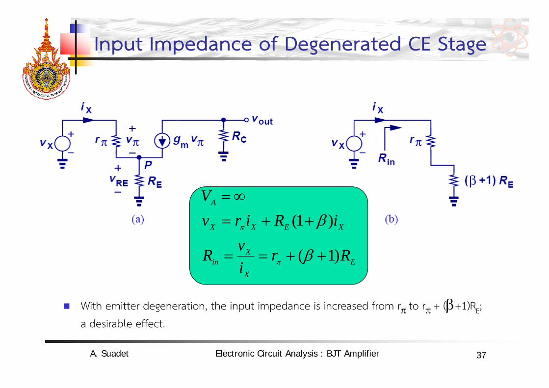
37
Input Impedance of Degenerated CE Stage
With emitter degeneration, the input impedance is increased from r to r + (+1)RE; a desirable effect.
EX
Xin
XEXX
A
RrivR
iRirvV
)1(
)1(
A. Suadet Electronic Circuit Analysis : BJT Amplifier
38
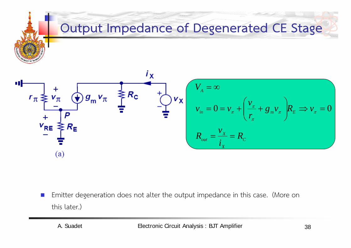
Output Impedance of Degenerated CE Stage
Emitter degeneration does not alter the output impedance in this case. (More on
this later.)
CX
Xout
Emin
A
RivR
vRvgrvvv
V
00
A. Suadet Electronic Circuit Analysis : BJT Amplifier
39
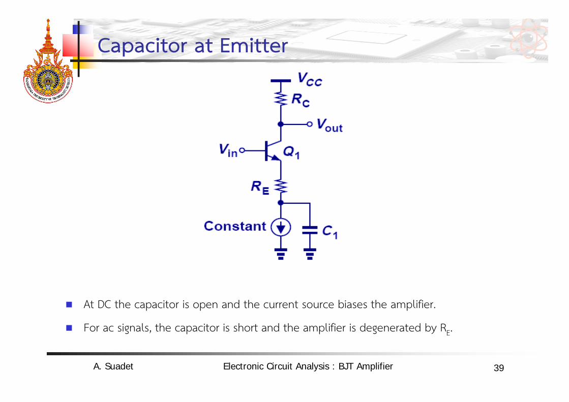
Capacitor at Emitter
At DC the capacitor is open and the current source biases the amplifier.
For ac signals, the capacitor is short and the amplifier is degenerated by RE.
A. Suadet Electronic Circuit Analysis : BJT Amplifier
40
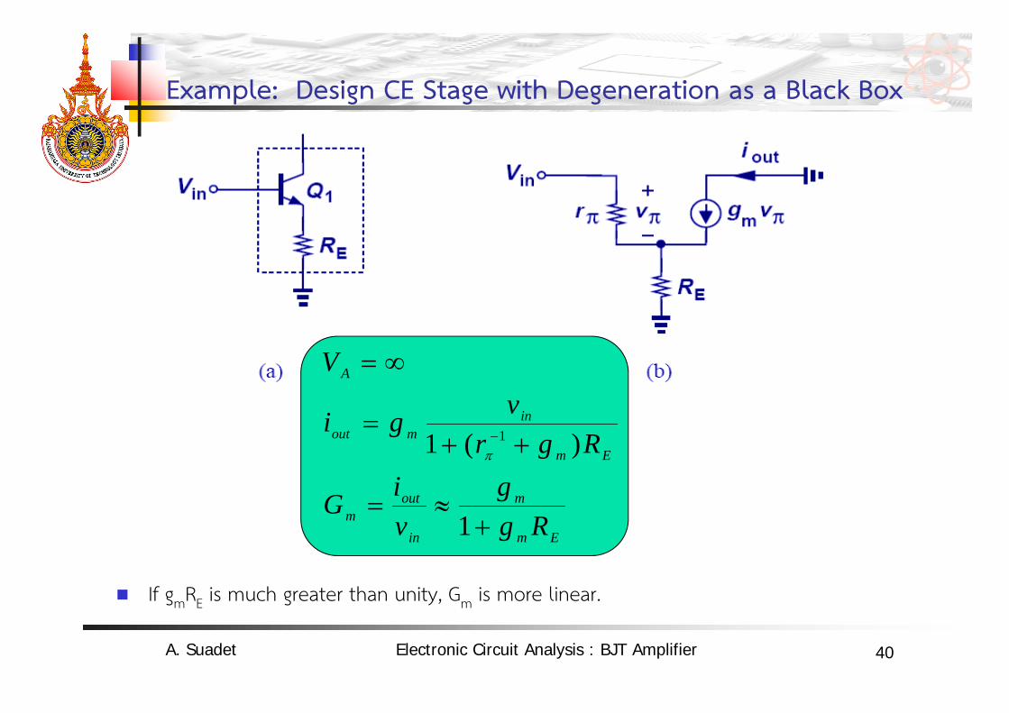
Example: Design CE Stage with Degeneration as a Black Box
If gmRE is much greater than unity, Gm is more linear.
Em
m
in
outm
Em
inmout
A
Rgg
viG
Rgrvgi
V
1
)(1 1
A. Suadet Electronic Circuit Analysis : BJT Amplifier
41
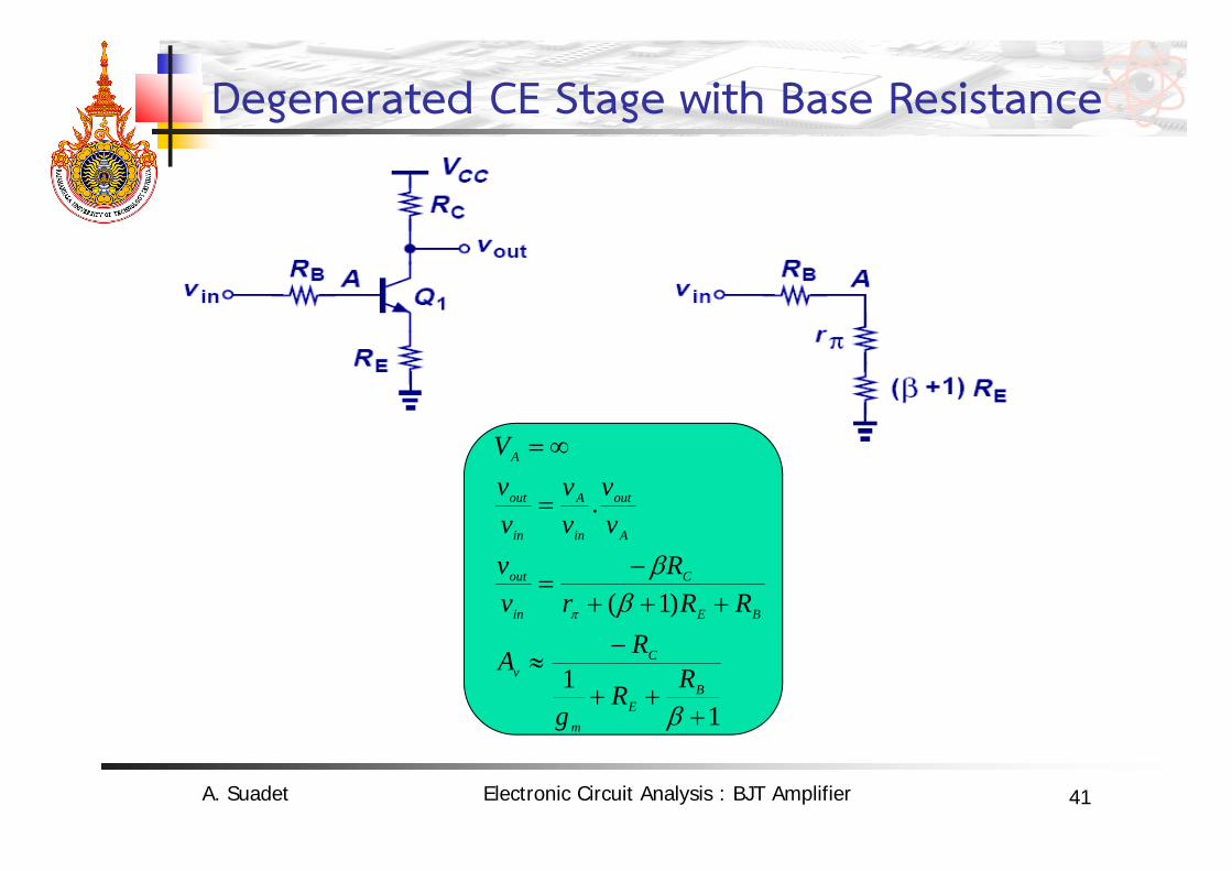
Degenerated CE Stage with Base Resistance
11
)1(
.
BE
m
Cv
BE
C
in
out
A
out
in
A
in
out
A
RRg
RA
RRrR
vv
vv
vv
vvV
A. Suadet Electronic Circuit Analysis : BJT Amplifier
42
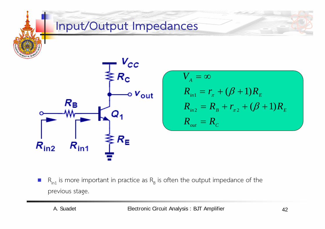
Input/Output Impedances
Rin1 is more important in practice as RB is often the output impedance of the
previous stage.
Cout
EBin
Ein
A
RRRrRR
RrRV
)1()1(
22
1
A. Suadet Electronic Circuit Analysis : BJT Amplifier
43
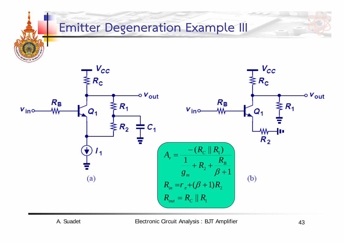
Emitter Degeneration Example III
1
2
2
1
||)1(
11
)||(
RRRRrR
RRg
RRA
Cout
in
B
m
Cv
A. Suadet Electronic Circuit Analysis : BJT Amplifier
44
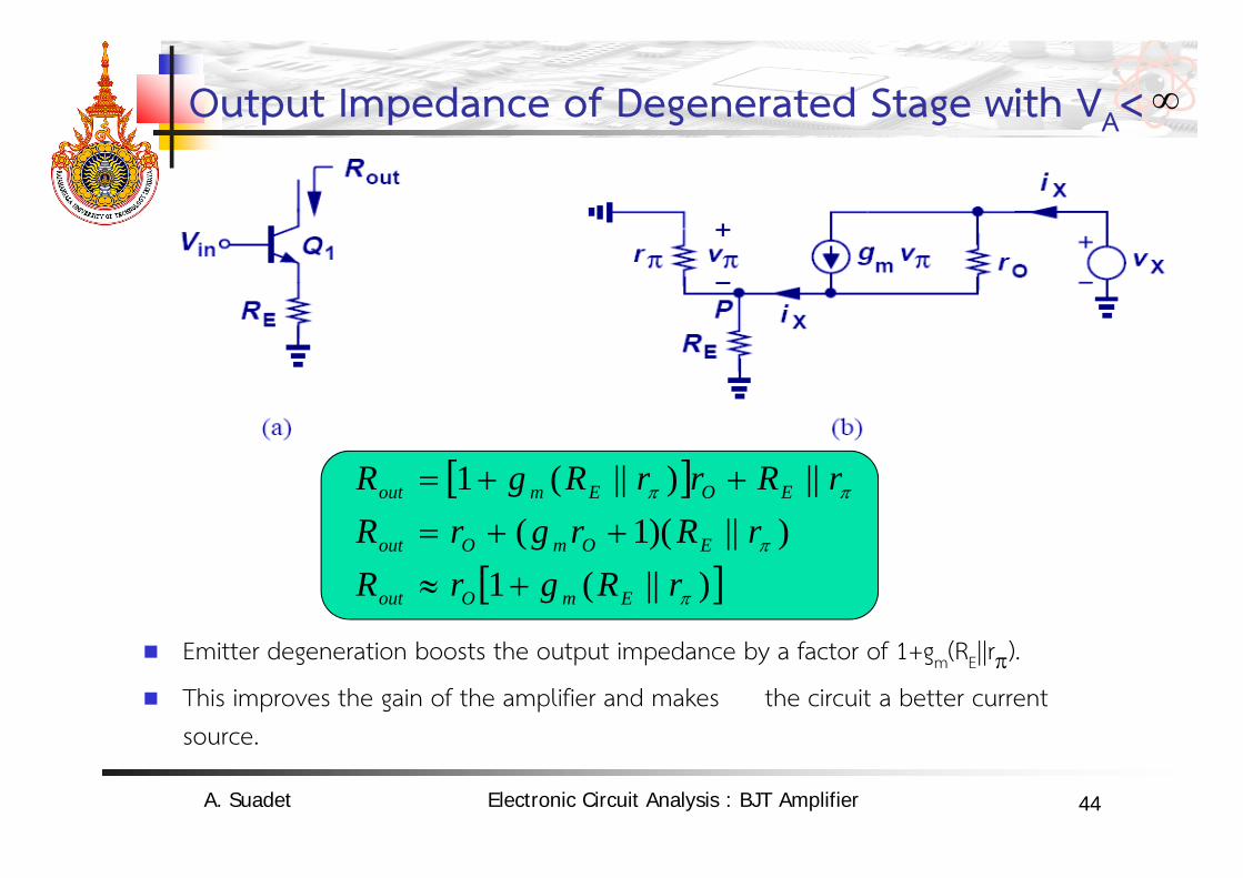
Output Impedance of Degenerated Stage with VA<
Emitter degeneration boosts the output impedance by a factor of 1+gm(RE||r).
This improves the gain of the amplifier and makes the circuit a better current source.
)||(1)||)(1(
||)||(1
rRgrRrRrgrR
rRrrRgR
EmOout
EOmOout
EOEmout
A. Suadet Electronic Circuit Analysis : BJT Amplifier
45
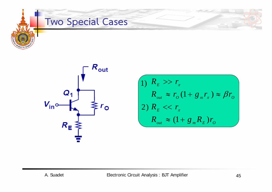
Two Special Cases
OEmout
E
OmOout
E
rRgRrR
rrgrRrR
)1(
)1(
)2
)1
A. Suadet Electronic Circuit Analysis : BJT Amplifier
46
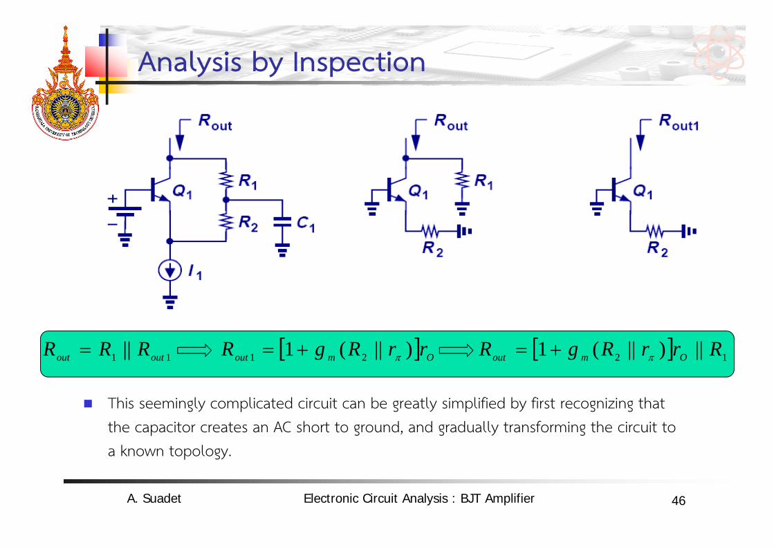
Analysis by Inspection
This seemingly complicated circuit can be greatly simplified by first recognizing that the capacitor creates an AC short to ground, and gradually transforming the circuit to a known topology.
12 ||)||(1 RrrRgR Omout Omout rrRgR )||(1 21 11 || outout RRR
A. Suadet Electronic Circuit Analysis : BJT Amplifier
47
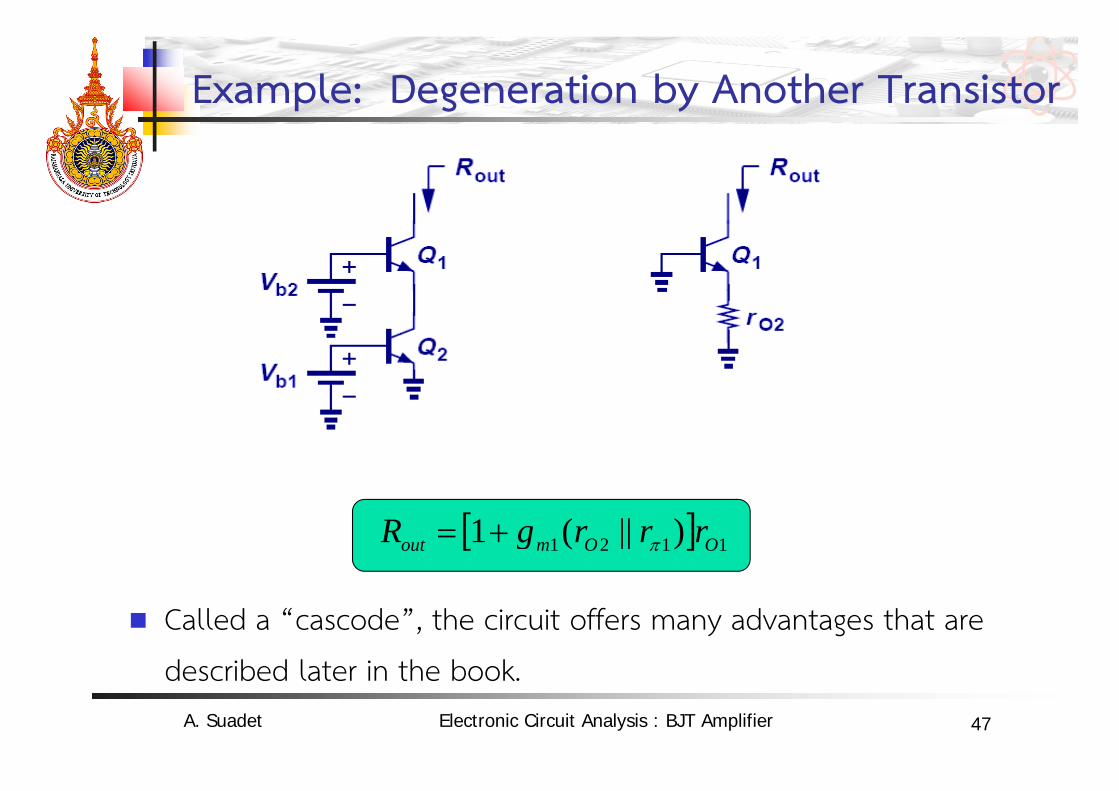
Example: Degeneration by Another Transistor
Called a “cascode”, the circuit offers many advantages that are
described later in the book.
1121 )||(1 OOmout rrrgR
A. Suadet Electronic Circuit Analysis : BJT Amplifier
48
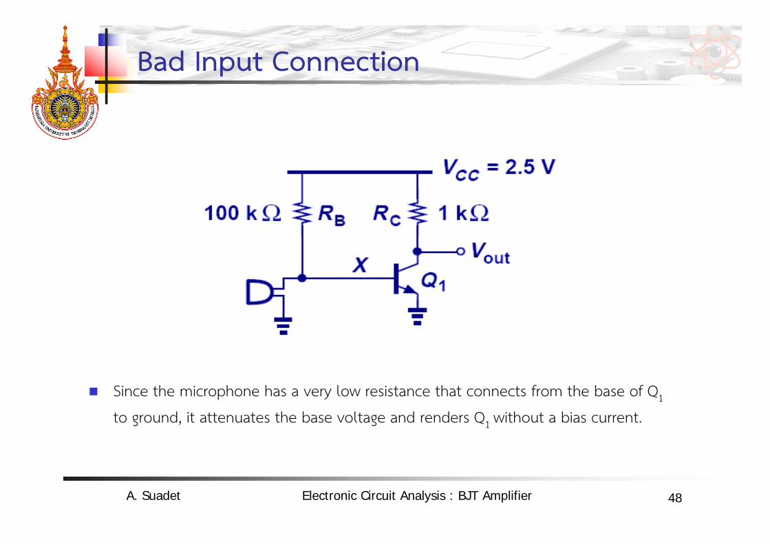
Bad Input Connection
Since the microphone has a very low resistance that connects from the base of Q1
to ground, it attenuates the base voltage and renders Q1 without a bias current.
A. Suadet Electronic Circuit Analysis : BJT Amplifier
49
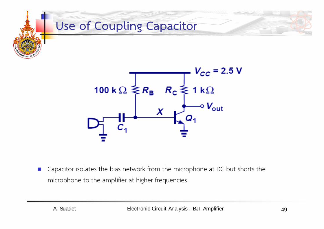
Use of Coupling Capacitor
Capacitor isolates the bias network from the microphone at DC but shorts the
microphone to the amplifier at higher frequencies.
A. Suadet Electronic Circuit Analysis : BJT Amplifier
50
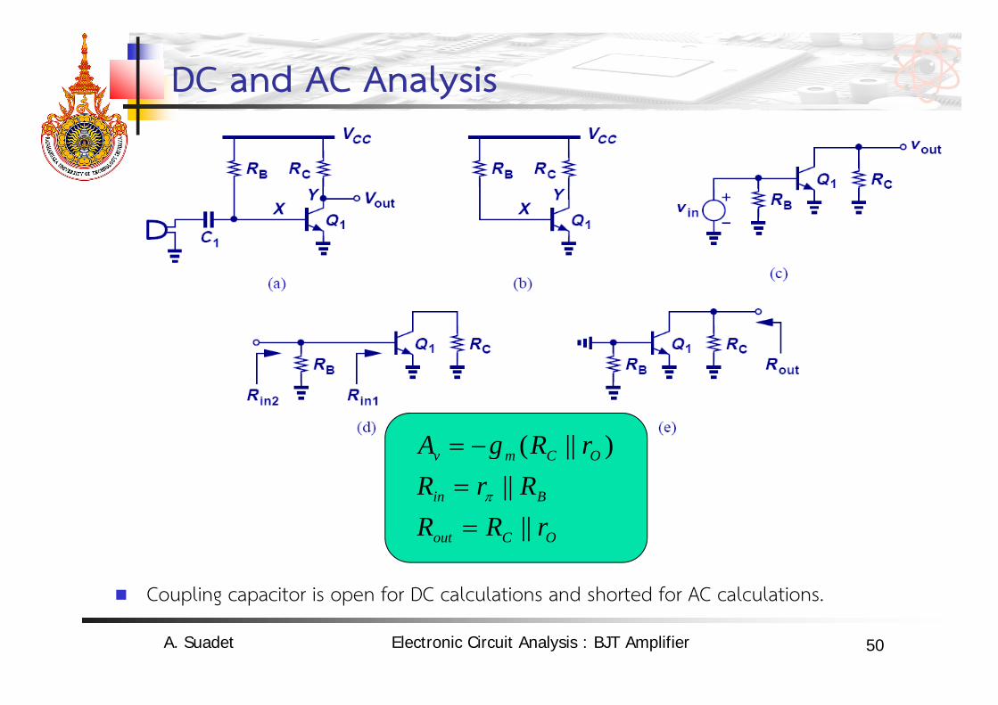
DC and AC Analysis
Coupling capacitor is open for DC calculations and shorted for AC calculations.
OCout
Bin
OCmv
rRRRrR
rRgA
||||
)||(
A. Suadet Electronic Circuit Analysis : BJT Amplifier
51
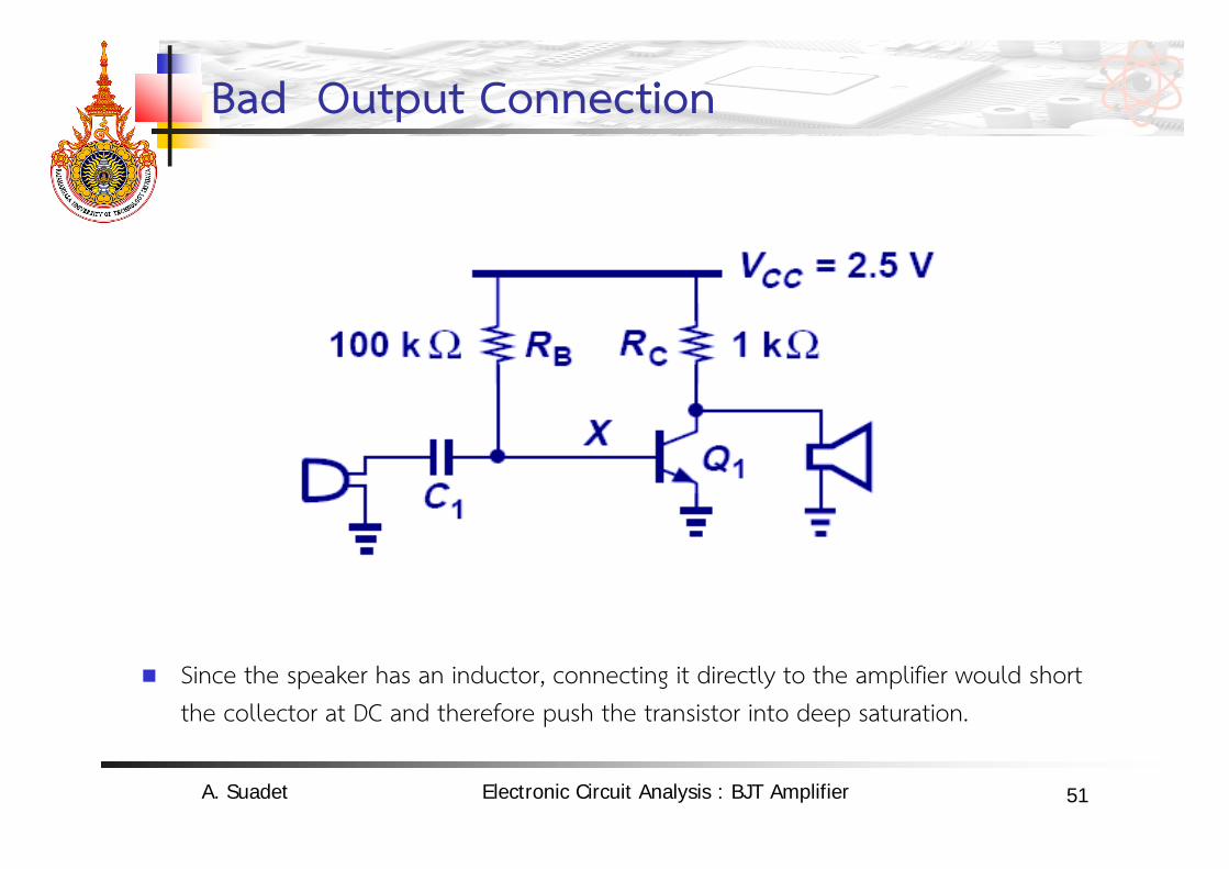
Bad Output Connection
Since the speaker has an inductor, connecting it directly to the amplifier would short the collector at DC and therefore push the transistor into deep saturation.
A. Suadet Electronic Circuit Analysis : BJT Amplifier
52
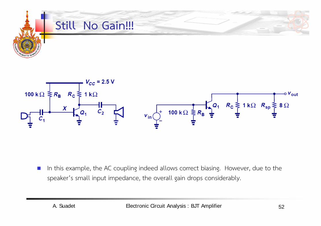
Still No Gain!!!
In this example, the AC coupling indeed allows correct biasing. However, due to the speaker’s small input impedance, the overall gain drops considerably.
A. Suadet Electronic Circuit Analysis : BJT Amplifier

53
CE Stage with Biasing
OCout
in
OCmv
rRRRRrRrRgA
||||||
)||(
21
A. Suadet Electronic Circuit Analysis : BJT Amplifier
54
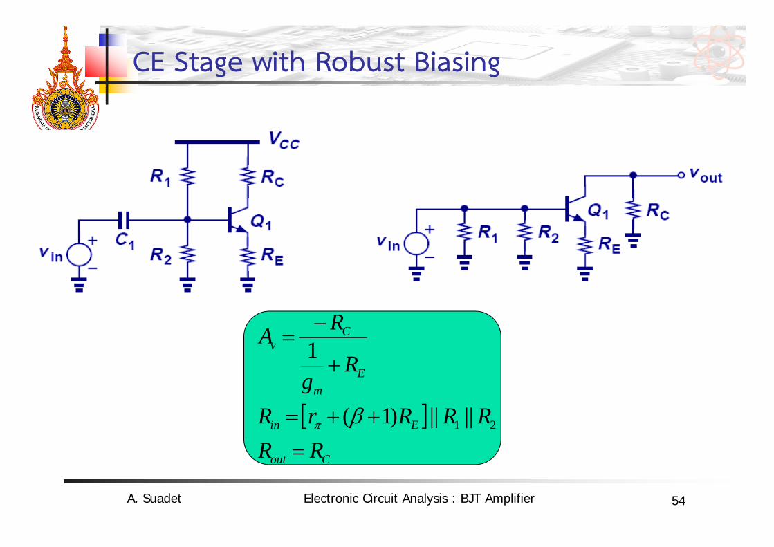
CE Stage with Robust Biasing
Cout
Ein
Em
Cv
RRRRRrR
Rg
RA
21 ||||)1(
1
AV
A. Suadet Electronic Circuit Analysis : BJT Amplifier
55
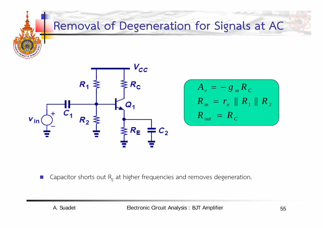
Removal of Degeneration for Signals at AC
Capacitor shorts out RE at higher frequencies and removes degeneration.
Cout
in
Cmv
RRRRrR
RgA
21 ||||
A. Suadet Electronic Circuit Analysis : BJT Amplifier
56
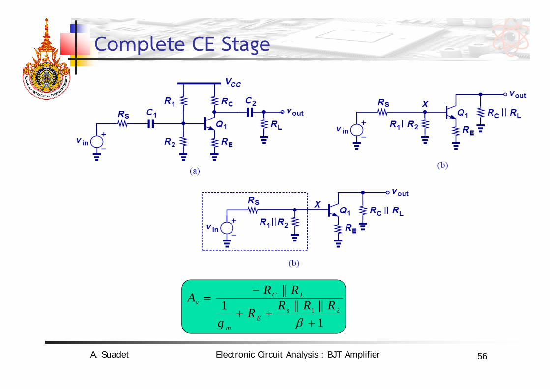
Complete CE Stage
1||||1
||21
RRRR
g
RRAs
Em
LCv
A. Suadet Electronic Circuit Analysis : BJT Amplifier
57
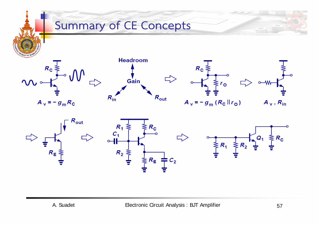
Summary of CE Concepts
A. Suadet Electronic Circuit Analysis : BJT Amplifier
58
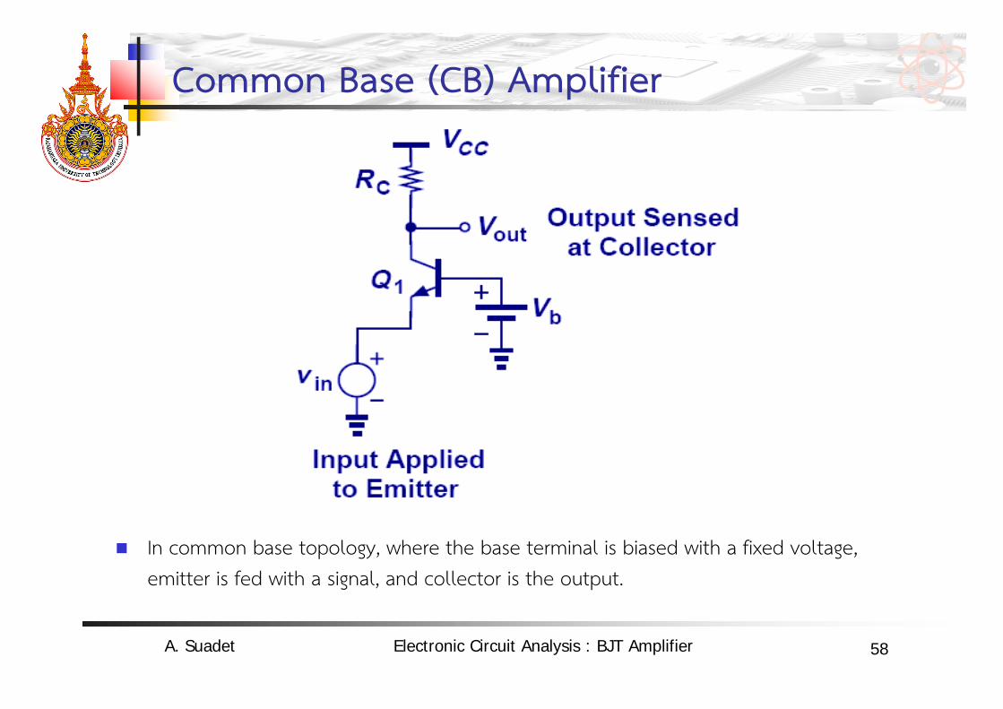
Common Base (CB) Amplifier
In common base topology, where the base terminal is biased with a fixed voltage, emitter is fed with a signal, and collector is the output.
A. Suadet Electronic Circuit Analysis : BJT Amplifier

59
CB Core
The voltage gain of CB stage is gmRC, which is identical to that of
CE stage in magnitude and opposite in phase.
Cmv RgA
A. Suadet Electronic Circuit Analysis : BJT Amplifier
60
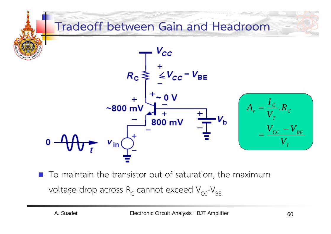
Tradeoff between Gain and Headroom
To maintain the transistor out of saturation, the maximum
voltage drop across RC cannot exceed VCC-VBE.
T
BECC
CT
Cv
VVV
RVIA
.
A. Suadet Electronic Circuit Analysis : BJT Amplifier
61
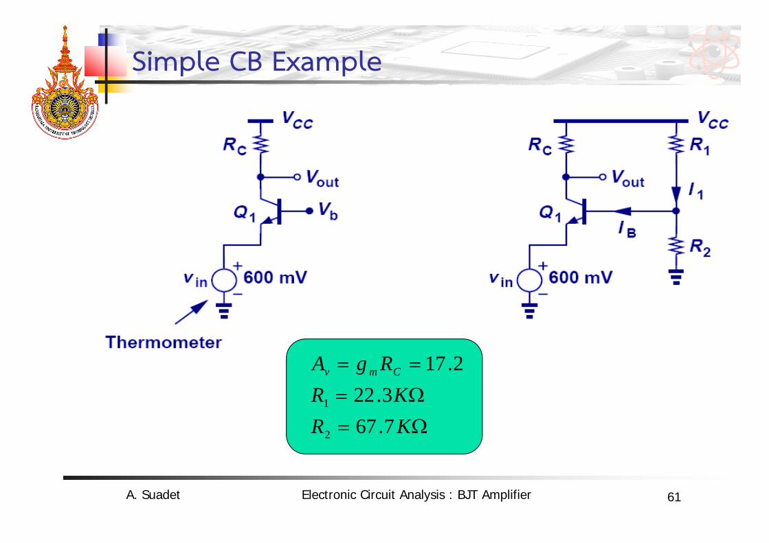
Simple CB Example
KRKR
RgA Cmv
7.673.22
2.17
2
1
A. Suadet Electronic Circuit Analysis : BJT Amplifier
62
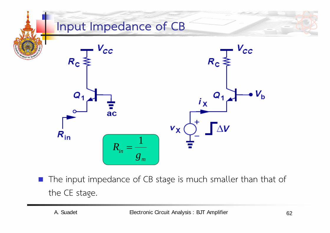
Input Impedance of CB
The input impedance of CB stage is much smaller than that of the CE stage.
min g
R 1
A. Suadet Electronic Circuit Analysis : BJT Amplifier
63
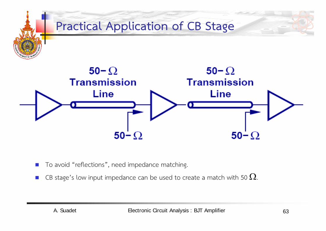
Practical Application of CB Stage
To avoid “reflections”, need impedance matching.
CB stage’s low input impedance can be used to create a match with 50 .
A. Suadet Electronic Circuit Analysis : BJT Amplifier
64
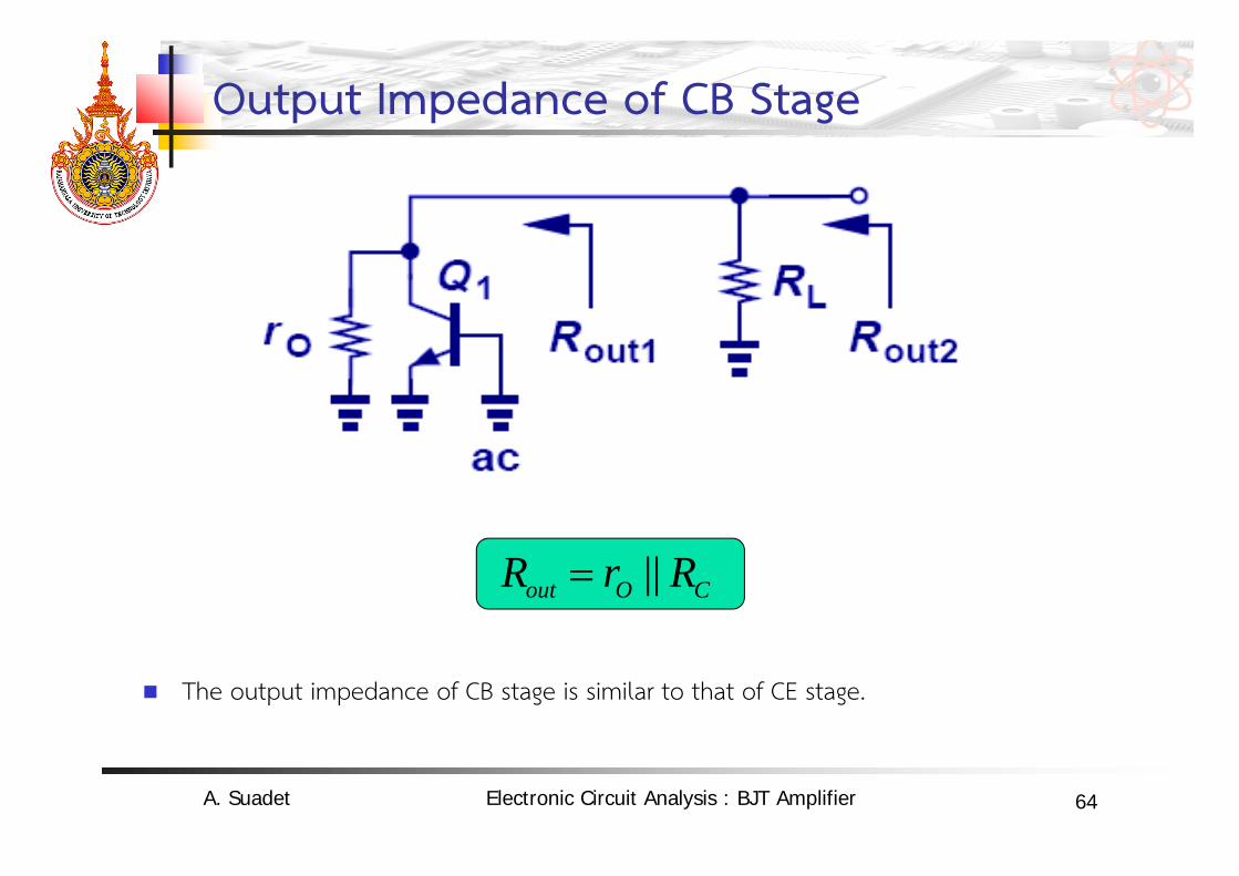
Output Impedance of CB Stage
The output impedance of CB stage is similar to that of CE stage.
COout RrR ||
A. Suadet Electronic Circuit Analysis : BJT Amplifier
65
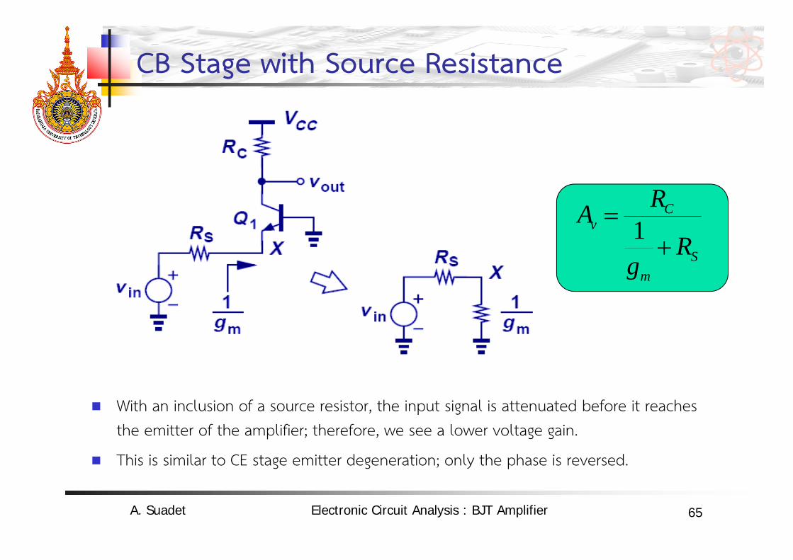
CB Stage with Source Resistance
With an inclusion of a source resistor, the input signal is attenuated before it reaches the emitter of the amplifier; therefore, we see a lower voltage gain.
This is similar to CE stage emitter degeneration; only the phase is reversed.
Sm
Cv
Rg
RA
1
A. Suadet Electronic Circuit Analysis : BJT Amplifier

66
Practical Example of CB Stage
An antenna usually has low output impedance; therefore, a correspondingly low input impedance is required for the following stage.
A. Suadet Electronic Circuit Analysis : BJT Amplifier
67
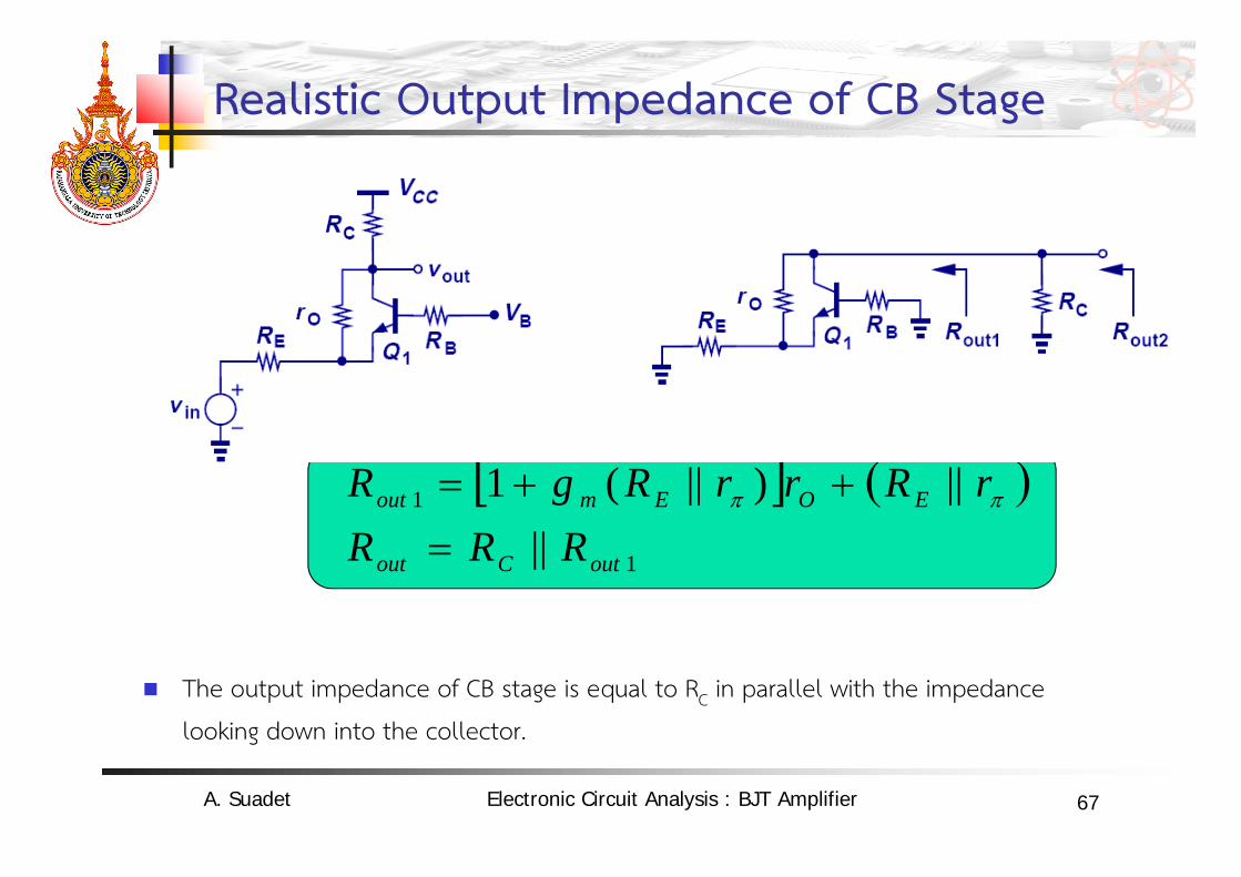
Realistic Output Impedance of CB Stage
The output impedance of CB stage is equal to RC in parallel with the impedance
looking down into the collector.
1
1
||||)||(1
outCout
EOEmout
RRRrRrrRgR
A. Suadet Electronic Circuit Analysis : BJT Amplifier

68
Output Impedance of CE and CB Stages
The output impedances of CE, CB stages are the same if both circuits are under the same condition. This is because when calculating output impedance, the input port is grounded, which renders the same circuit for both CE and CB stages.
A. Suadet Electronic Circuit Analysis : BJT Amplifier
69
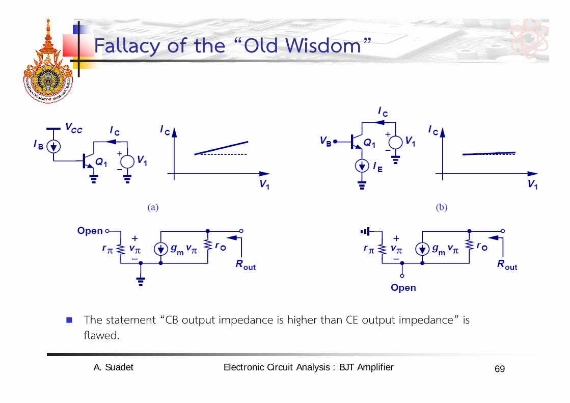
Fallacy of the “Old Wisdom”
The statement “CB output impedance is higher than CE output impedance” is flawed.
A. Suadet Electronic Circuit Analysis : BJT Amplifier

70
CB with Base Resistance
With an addition of base resistance, the voltage gain degrades.
m
BE
C
in
out
gRR
Rvv
11
A. Suadet Electronic Circuit Analysis : BJT Amplifier
71
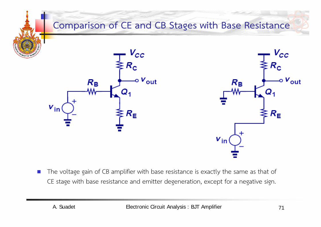
Comparison of CE and CB Stages with Base Resistance
The voltage gain of CB amplifier with base resistance is exactly the same as that of CE stage with base resistance and emitter degeneration, except for a negative sign.
A. Suadet Electronic Circuit Analysis : BJT Amplifier
72
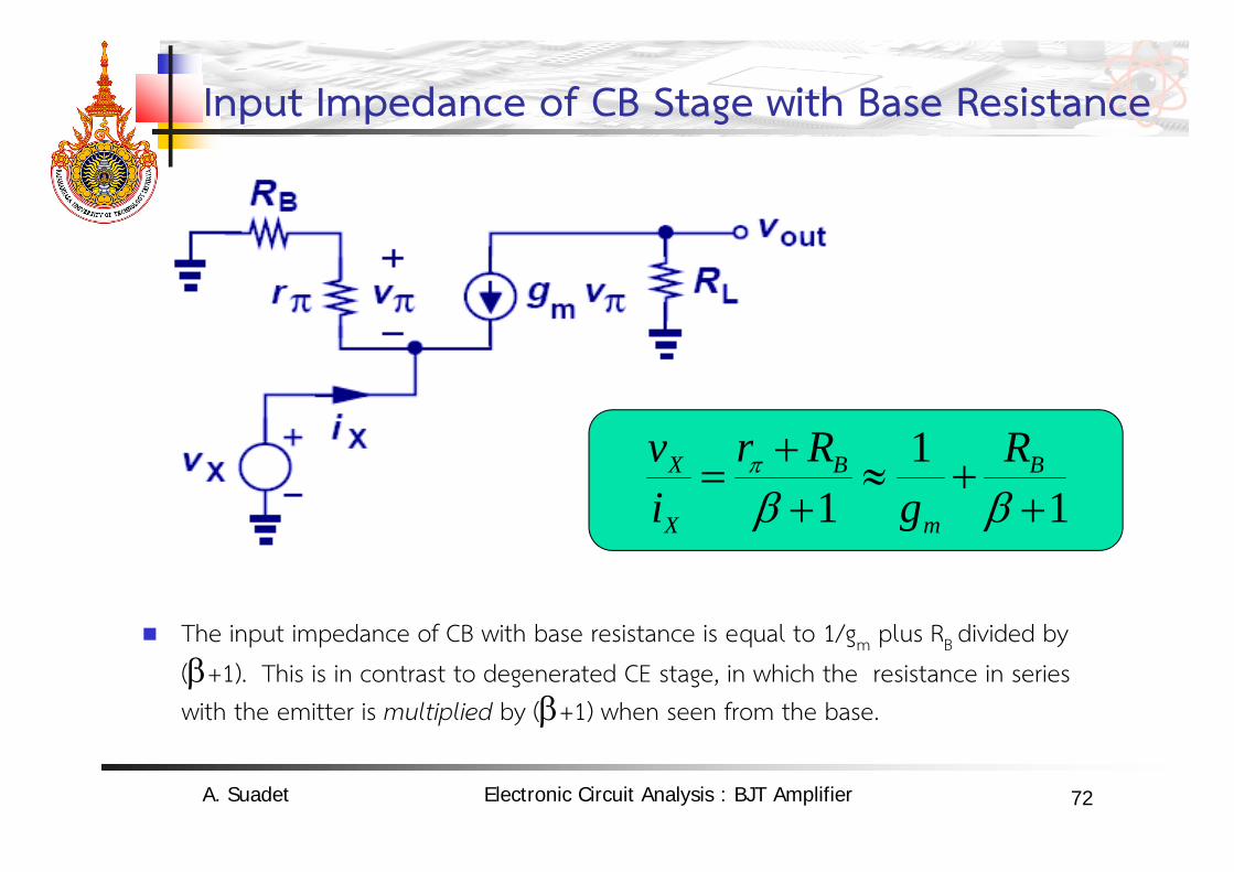
Input Impedance of CB Stage with Base Resistance
The input impedance of CB with base resistance is equal to 1/gm plus RB divided by (+1). This is in contrast to degenerated CE stage, in which the resistance in series with the emitter is multiplied by (+1) when seen from the base.
11
1
B
m
B
X
X Rg
Rriv
A. Suadet Electronic Circuit Analysis : BJT Amplifier
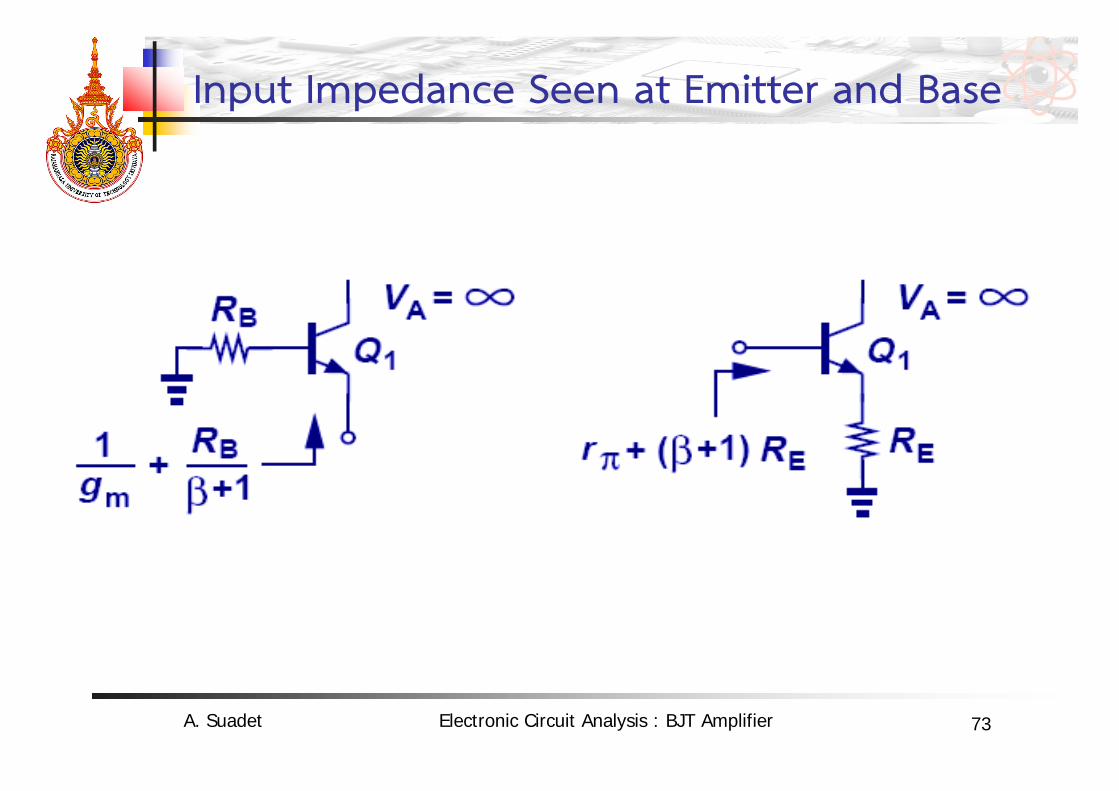
73
Input Impedance Seen at Emitter and Base
A. Suadet Electronic Circuit Analysis : BJT Amplifier
74
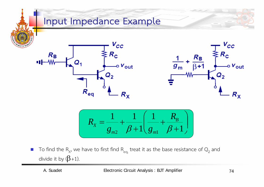
Input Impedance Example
To find the RX, we have to first find Req, treat it as the base resistance of Q2 and
divide it by (+1).
1
11
1112
B
mmX
Rgg
R
A. Suadet Electronic Circuit Analysis : BJT Amplifier
75
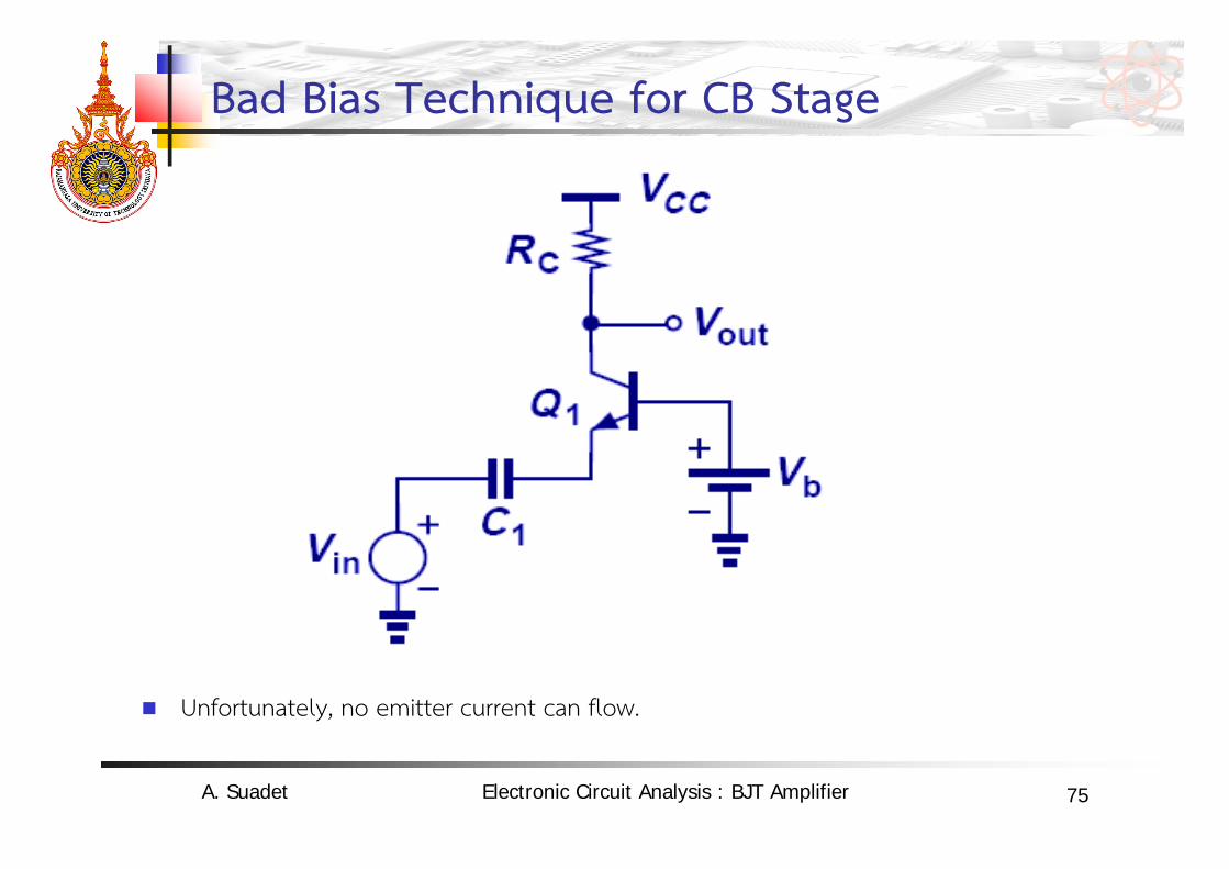
Bad Bias Technique for CB Stage
Unfortunately, no emitter current can flow.
A. Suadet Electronic Circuit Analysis : BJT Amplifier
76
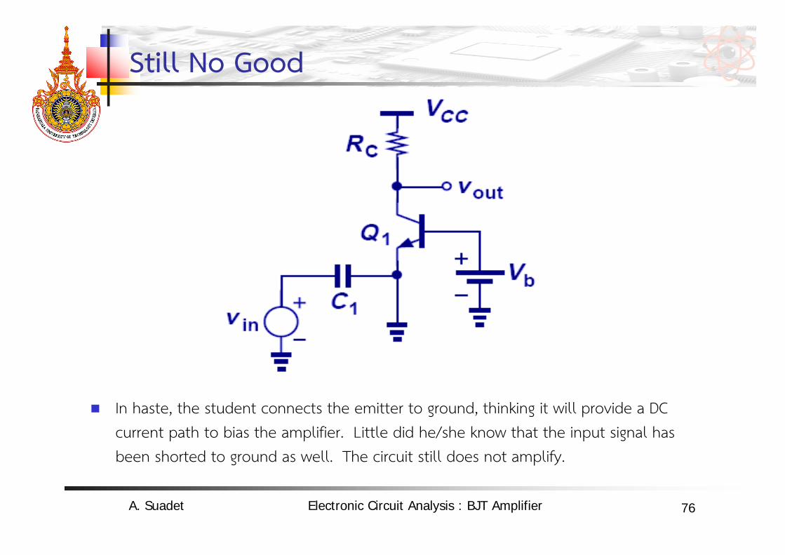
Still No Good
In haste, the student connects the emitter to ground, thinking it will provide a DC current path to bias the amplifier. Little did he/she know that the input signal has been shorted to ground as well. The circuit still does not amplify.
A. Suadet Electronic Circuit Analysis : BJT Amplifier
77
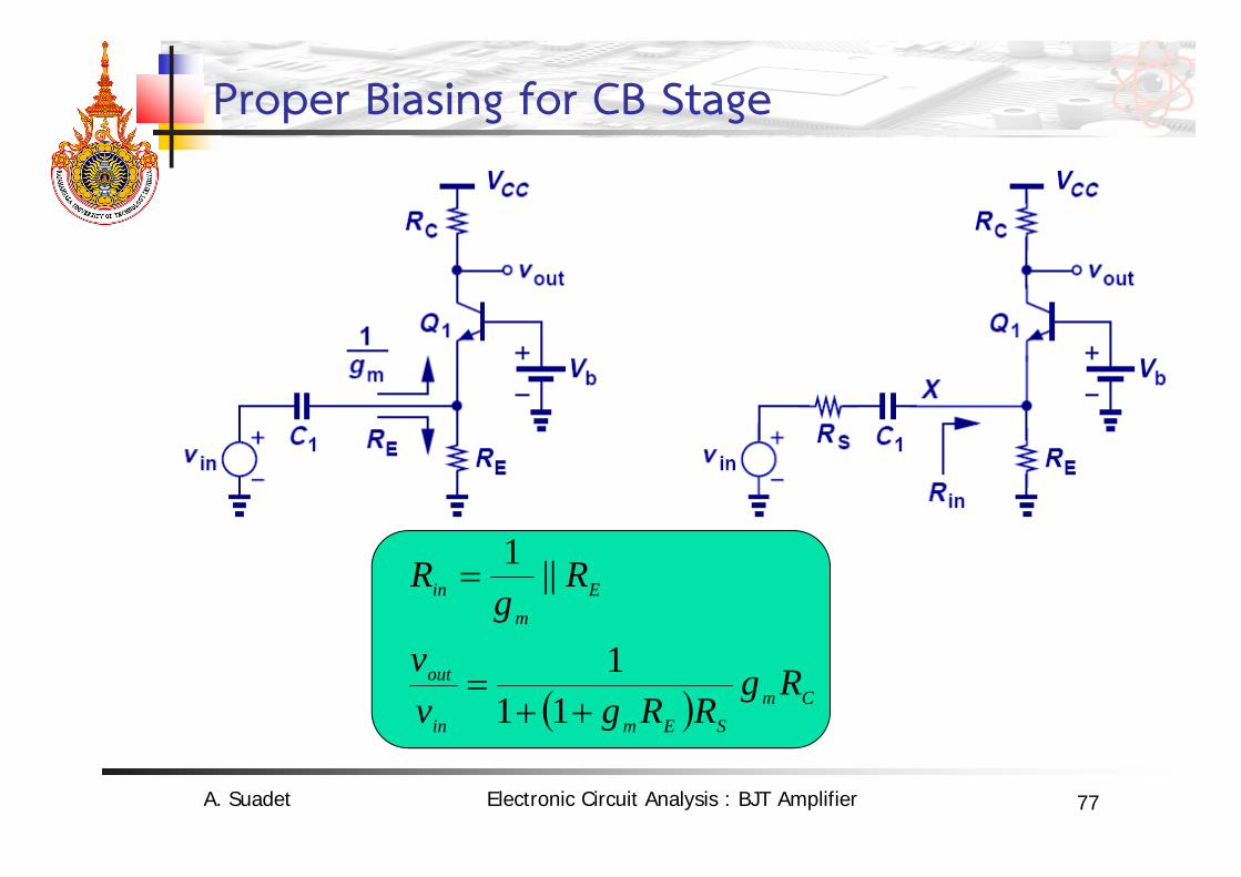
Proper Biasing for CB Stage
CmSEmin
out
Em
in
RgRRgv
v
Rg
R
111
||1
A. Suadet Electronic Circuit Analysis : BJT Amplifier
78
Reduction of Input Impedance Due to RE
The reduction of input impedance due to RE is bad because it shunts part of the input current to ground instead of to Q1 (and Rc) .
A. Suadet Electronic Circuit Analysis : BJT Amplifier
79
Creation of Vb
Resistive divider lowers the gain.
To remedy this problem, a capacitor is inserted from base to ground to short out the
resistor divider at the frequency of interest.
A. Suadet Electronic Circuit Analysis : BJT Amplifier
80
Example of CB Stage with Bias
For the circuit shown above, RE >> 1/gm.
R1 and R2 are chosen so that Vb is at the appropriate value and the current that flows thru the divider is much larger than the base current.
Capacitors are chosen to be small compared to 1/gm at the required frequency.
A. Suadet Electronic Circuit Analysis : BJT Amplifier
81
Emitter Follower (Common Collector Amplifier)
A. Suadet Electronic Circuit Analysis : BJT Amplifier
82
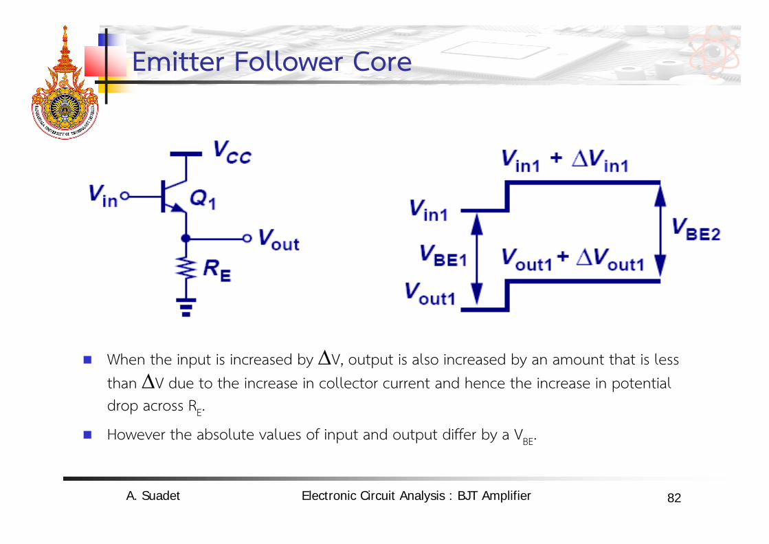
Emitter Follower Core
When the input is increased by V, output is also increased by an amount that is less than V due to the increase in collector current and hence the increase in potential drop across RE.
However the absolute values of input and output differ by a VBE.
A. Suadet Electronic Circuit Analysis : BJT Amplifier

83
Small-Signal Model of Emitter Follower
As shown above, the voltage gain is less than unity and positive.
mE
E
E
in
out
gR
R
Rrv
v11
11
1
AV
A. Suadet Electronic Circuit Analysis : BJT Amplifier
84
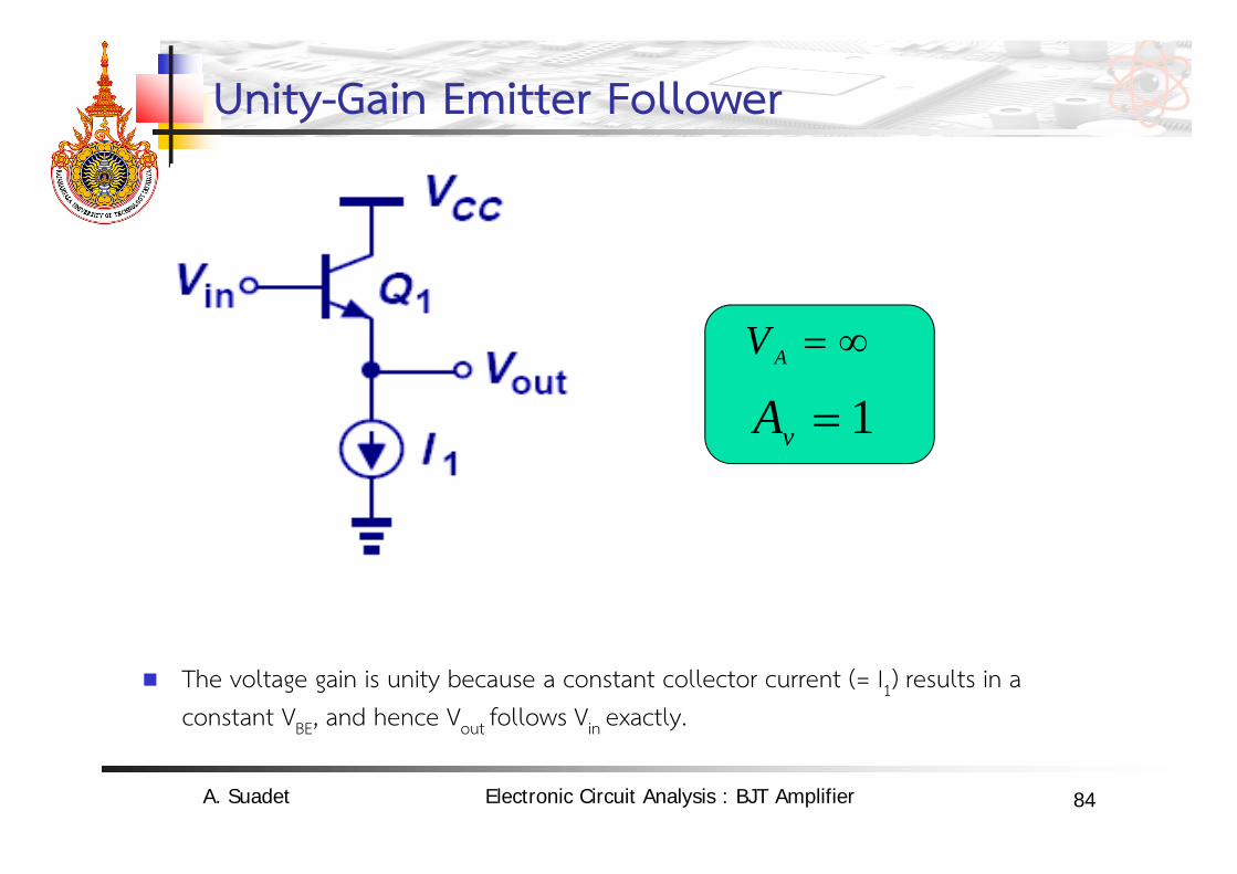
Unity-Gain Emitter Follower
The voltage gain is unity because a constant collector current (= I1) results in a constant VBE, and hence Vout follows Vin exactly.
1vAAV
A. Suadet Electronic Circuit Analysis : BJT Amplifier
85
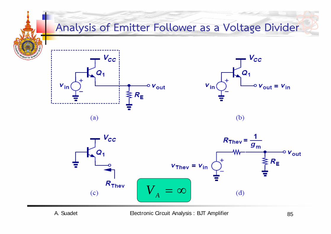
Analysis of Emitter Follower as a Voltage Divider
AVA. Suadet Electronic Circuit Analysis : BJT Amplifier
86
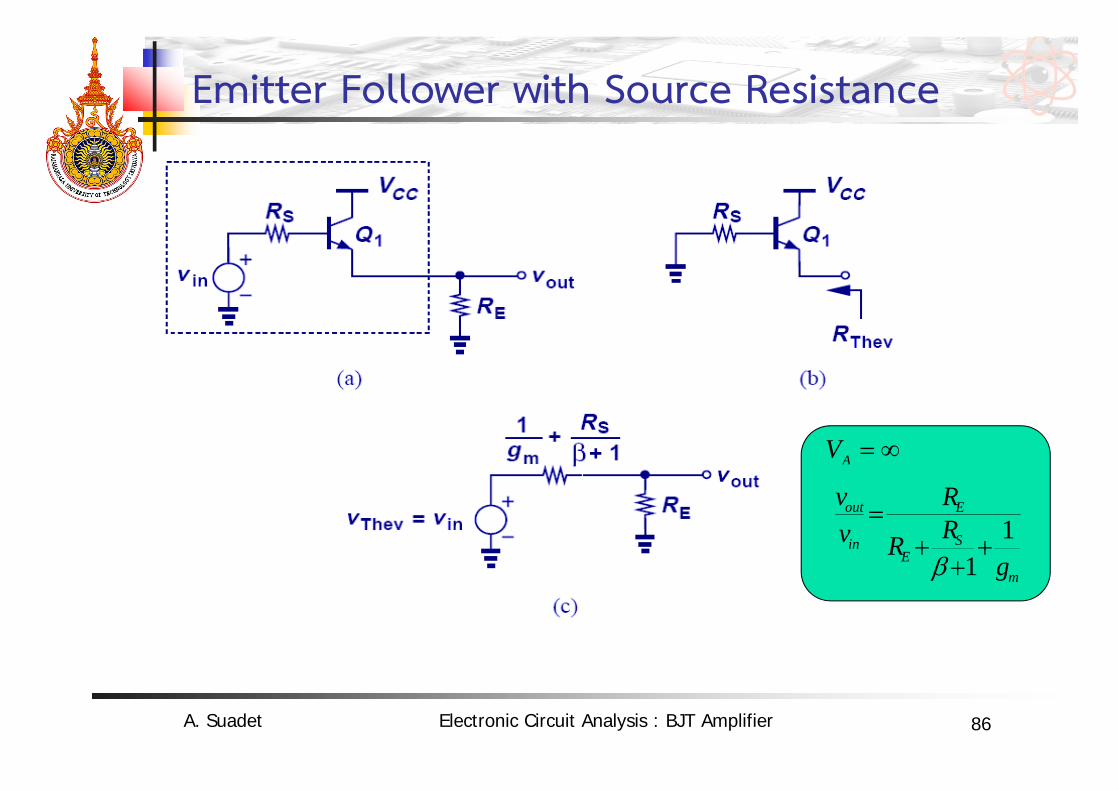
Emitter Follower with Source Resistance
m
SE
E
in
out
gRR
Rvv
11
AV
A. Suadet Electronic Circuit Analysis : BJT Amplifier
87
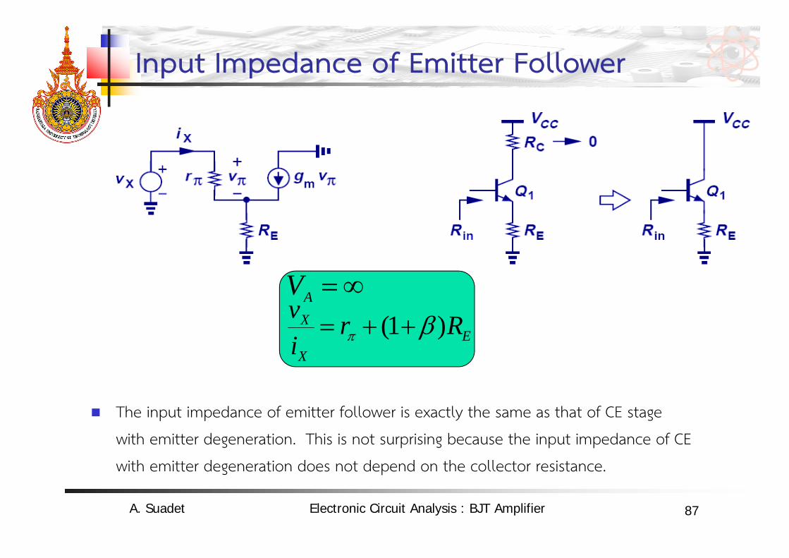
Input Impedance of Emitter Follower
The input impedance of emitter follower is exactly the same as that of CE stage
with emitter degeneration. This is not surprising because the input impedance of CE
with emitter degeneration does not depend on the collector resistance.
EX
X Rriv )1(
AV
A. Suadet Electronic Circuit Analysis : BJT Amplifier
88
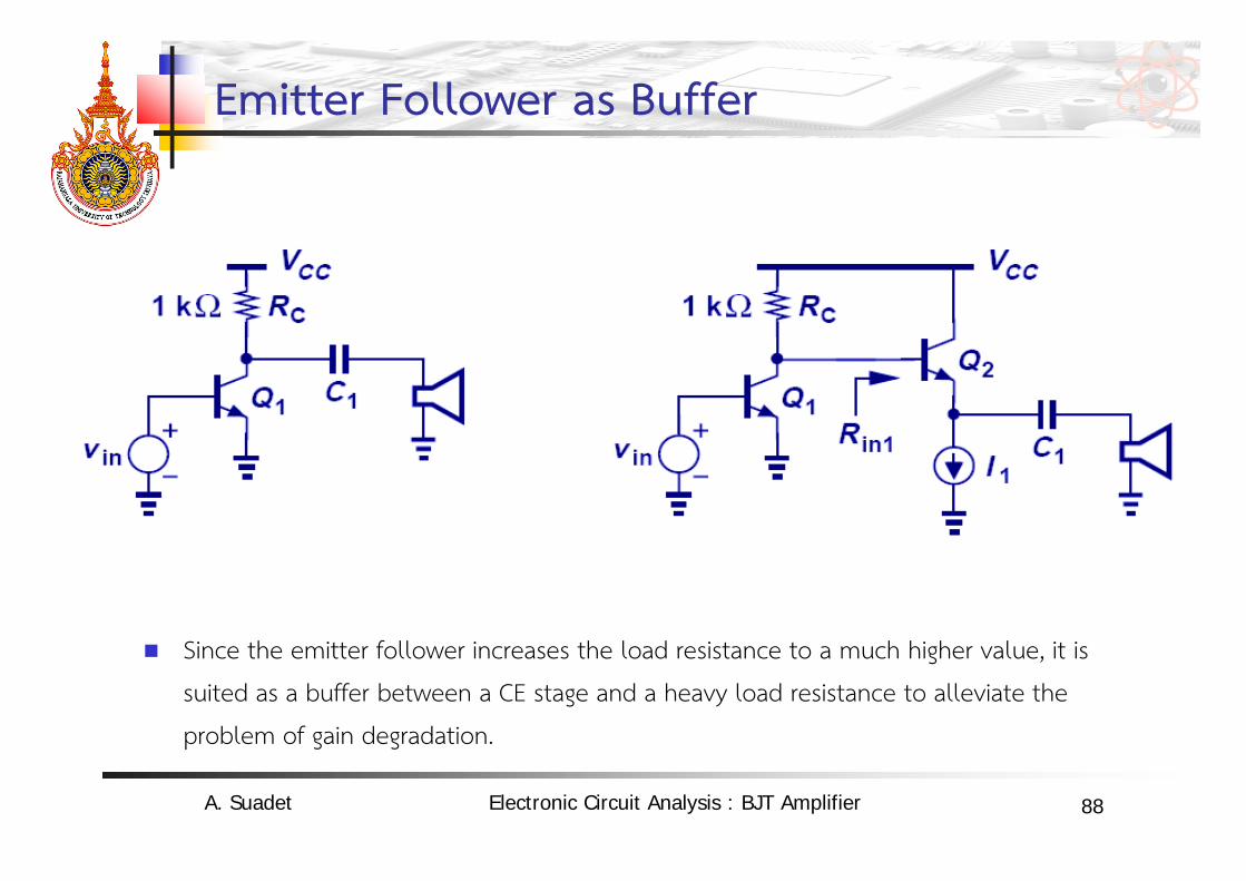
Emitter Follower as Buffer
Since the emitter follower increases the load resistance to a much higher value, it is
suited as a buffer between a CE stage and a heavy load resistance to alleviate the
problem of gain degradation.
A. Suadet Electronic Circuit Analysis : BJT Amplifier
89
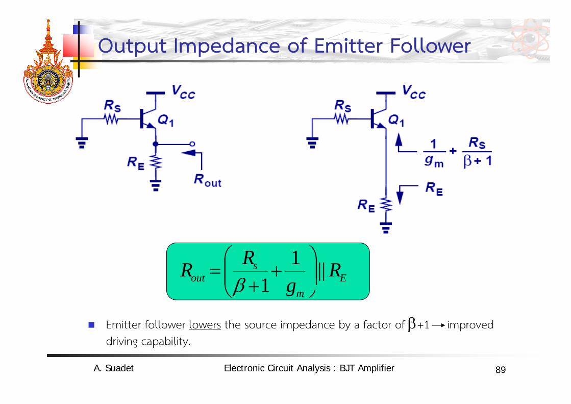
Output Impedance of Emitter Follower
Emitter follower lowers the source impedance by a factor of +1 improved driving capability.
Em
sout R
gRR ||1
1
A. Suadet Electronic Circuit Analysis : BJT Amplifier
90
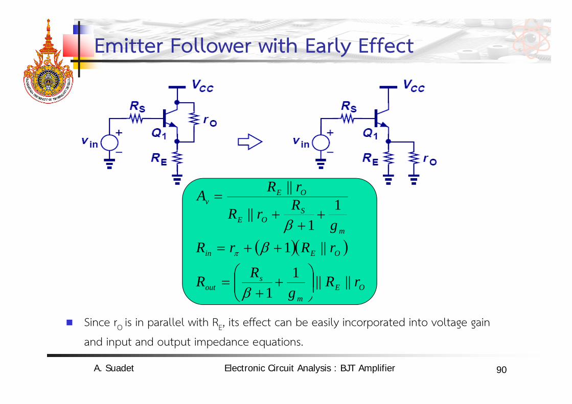
Emitter Follower with Early Effect
Since rO is in parallel with RE, its effect can be easily incorporated into voltage gain
and input and output impedance equations.
OEm
sout
OEin
m
SOE
OEv
rRg
RR
rRrRg
RrR
rRA
||||11
||1
11
||
||
A. Suadet Electronic Circuit Analysis : BJT Amplifier
91
Current Gain
There is a current gain of (+1) from base to emitter.
Effectively speaking, the load resistance is multiplied by (+1) as seen from the base.
A. Suadet Electronic Circuit Analysis : BJT Amplifier
92
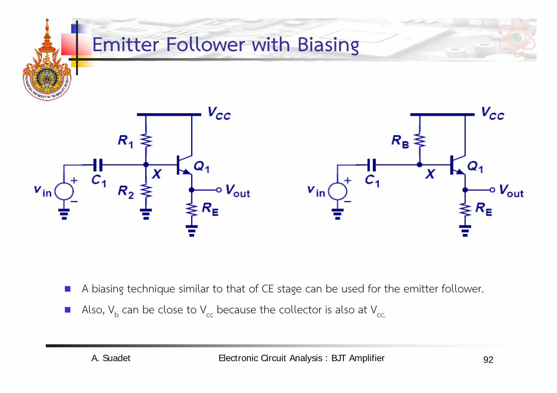
Emitter Follower with Biasing
A biasing technique similar to that of CE stage can be used for the emitter follower.
Also, Vb can be close to Vcc because the collector is also at Vcc.
A. Suadet Electronic Circuit Analysis : BJT Amplifier
93
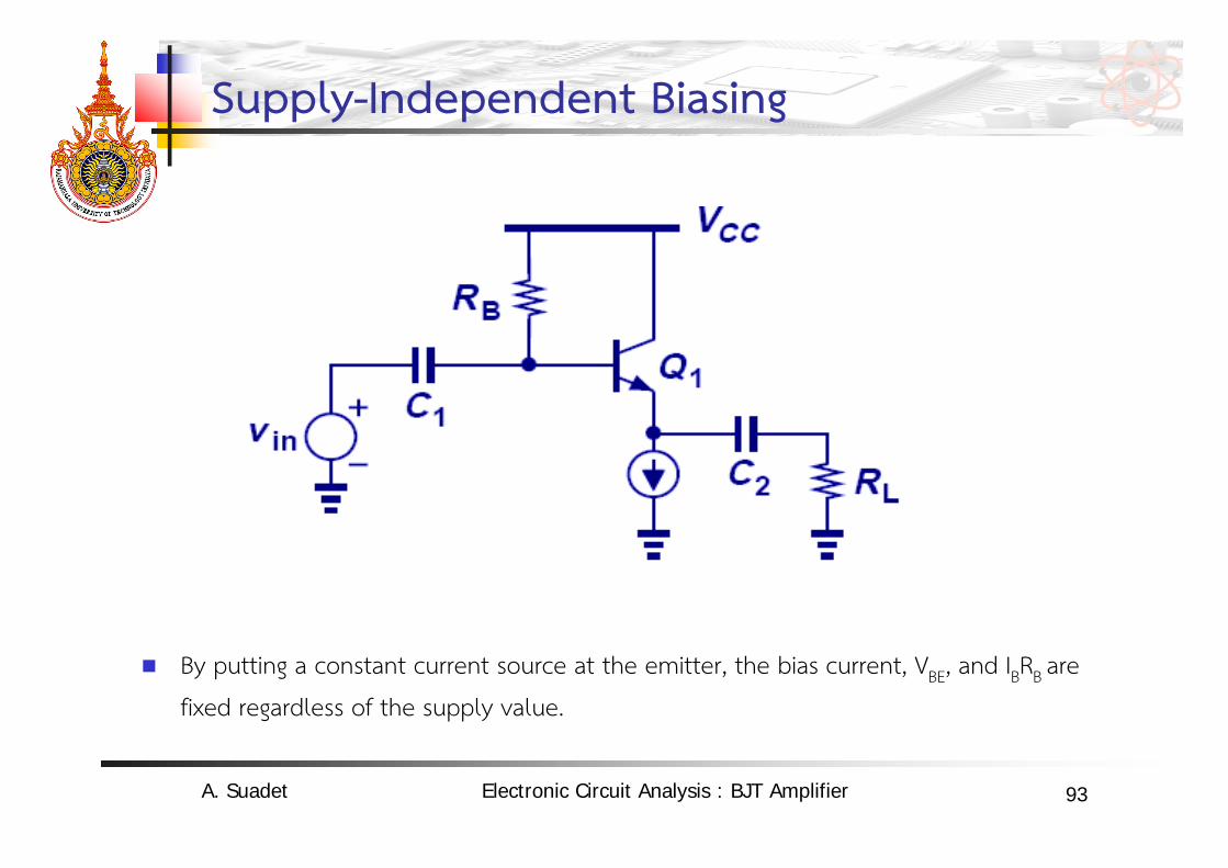
Supply-Independent Biasing
By putting a constant current source at the emitter, the bias current, VBE, and IBRB are
fixed regardless of the supply value.
A. Suadet Electronic Circuit Analysis : BJT Amplifier
94
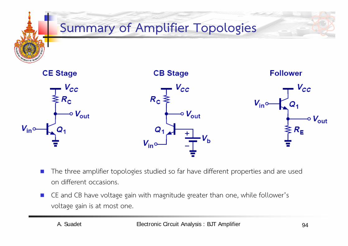
Summary of Amplifier Topologies
The three amplifier topologies studied so far have different properties and are used on different occasions.
CE and CB have voltage gain with magnitude greater than one, while follower’s voltage gain is at most one.
A. Suadet Electronic Circuit Analysis : BJT Amplifier
95
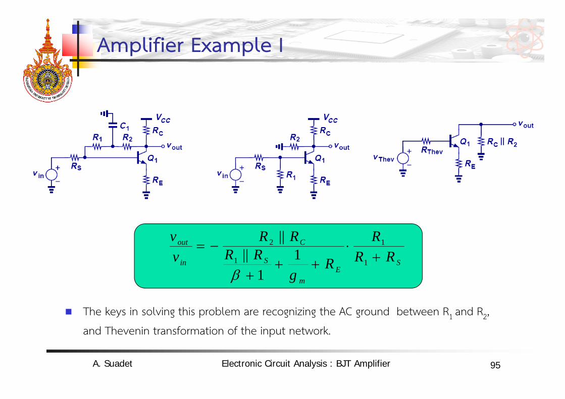
Amplifier Example I
The keys in solving this problem are recognizing the AC ground between R1 and R2,
and Thevenin transformation of the input network.
SE
m
S
C
in
out
RRR
Rg
RRRR
vv
1
1
1
2
11
||||
A. Suadet Electronic Circuit Analysis : BJT Amplifier
96
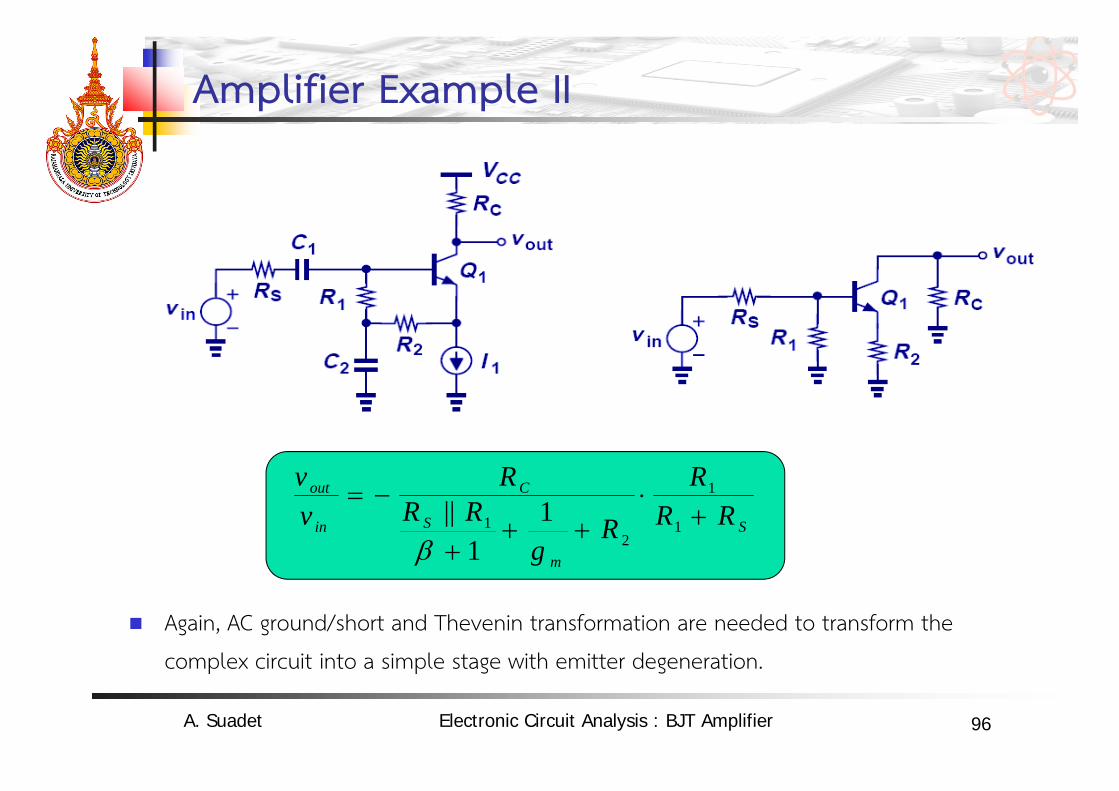
Amplifier Example II
Again, AC ground/short and Thevenin transformation are needed to transform the
complex circuit into a simple stage with emitter degeneration.
S
m
S
C
in
out
RRR
Rg
RRR
vv
1
1
21 1
1||
A. Suadet Electronic Circuit Analysis : BJT Amplifier
97
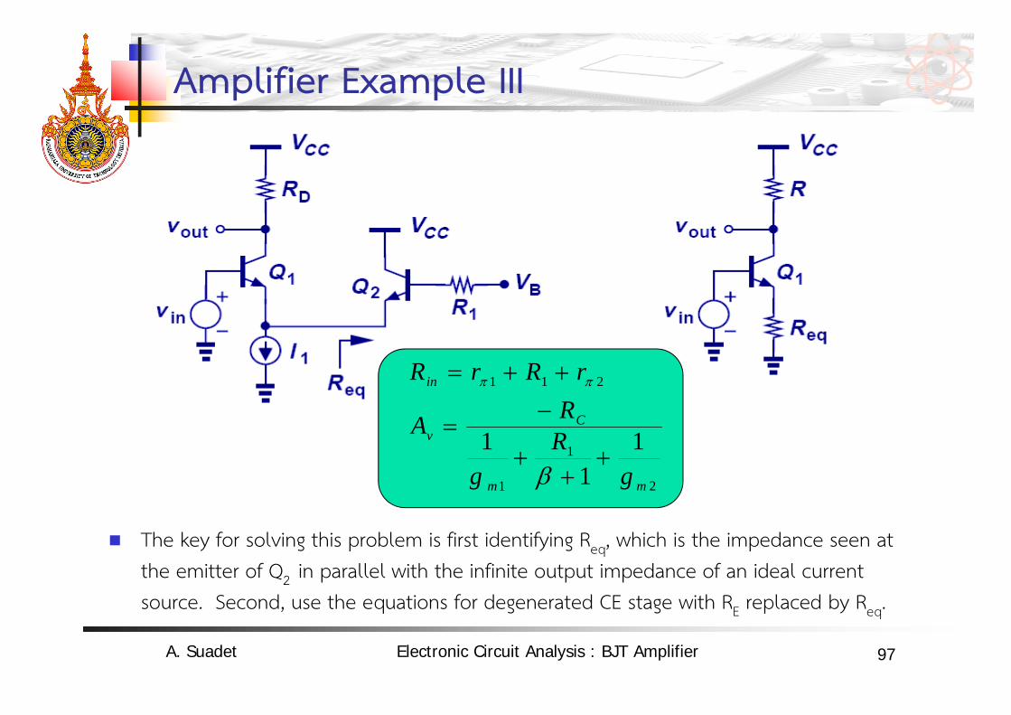
Amplifier Example III
The key for solving this problem is first identifying Req, which is the impedance seen at the emitter of Q2 in parallel with the infinite output impedance of an ideal current source. Second, use the equations for degenerated CE stage with RE replaced by Req.
2
1
1
211
11
1mm
Cv
in
gR
g
RA
rRrR
A. Suadet Electronic Circuit Analysis : BJT Amplifier
98
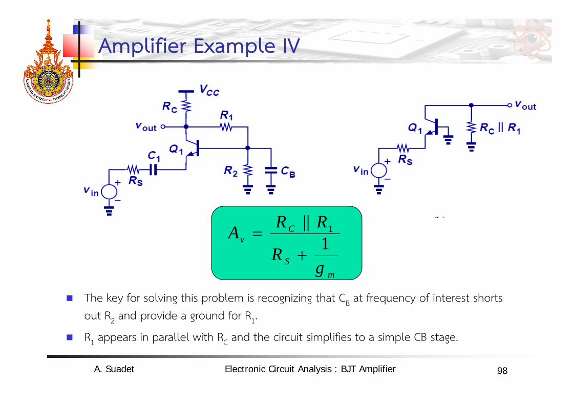
Amplifier Example IV
The key for solving this problem is recognizing that CB at frequency of interest shorts out R2 and provide a ground for R1.
R1 appears in parallel with RC and the circuit simplifies to a simple CB stage.
mS
Cv
gR
RRA 1|| 1
A. Suadet Electronic Circuit Analysis : BJT Amplifier
99
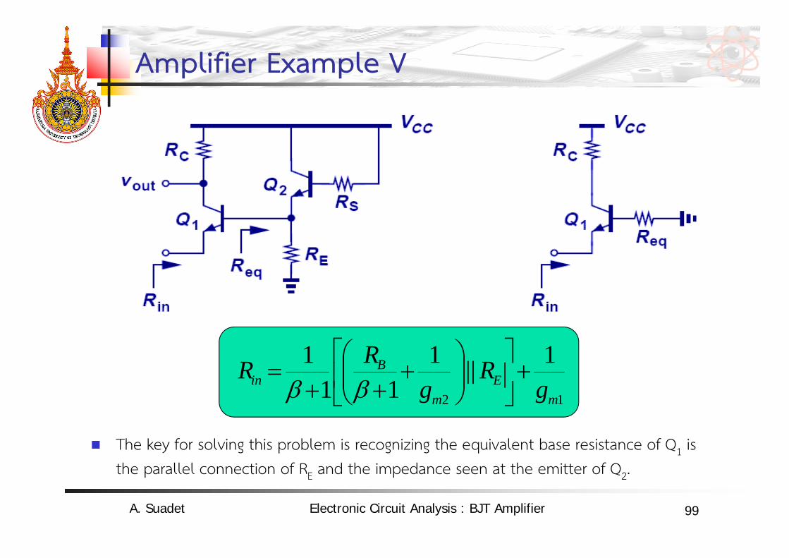
Amplifier Example V
The key for solving this problem is recognizing the equivalent base resistance of Q1 is the parallel connection of RE and the impedance seen at the emitter of Q2.
12
1||111
1m
Em
Bin g
Rg
RR
A. Suadet Electronic Circuit Analysis : BJT Amplifier
100
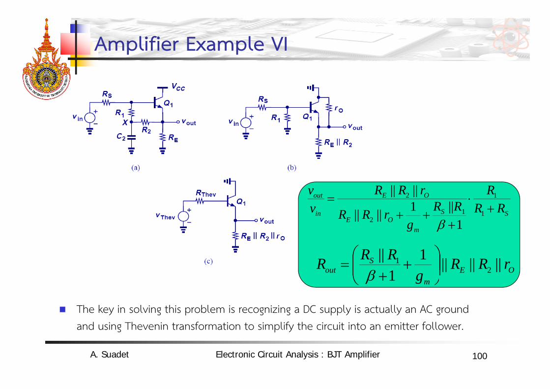
Amplifier Example VI
The key in solving this problem is recognizing a DC supply is actually an AC ground and using Thevenin transformation to simplify the circuit into an emitter follower.
SS
mOE
OE
in
out
RRR
RRg
rRR
rRRvv
1
1
12
2
1||1||||
||||
OEm
Sout rRR
gRRR ||||||11
||2
1
A. Suadet Electronic Circuit Analysis : BJT Amplifier
101
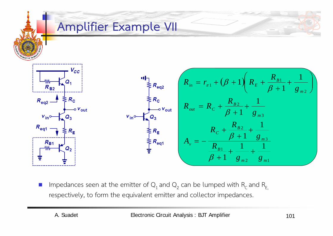
Amplifier Example VII
Impedances seen at the emitter of Q1 and Q2 can be lumped with RC and RE,
respectively, to form the equivalent emitter and collector impedances.
12
1
3
2
3
2
2
11
111
11
11
11
1
mm
B
m
BC
v
m
BCout
m
BEin
ggR
gRR
A
gRRR
gRRrR
A. Suadet Electronic Circuit Analysis : BJT Amplifier
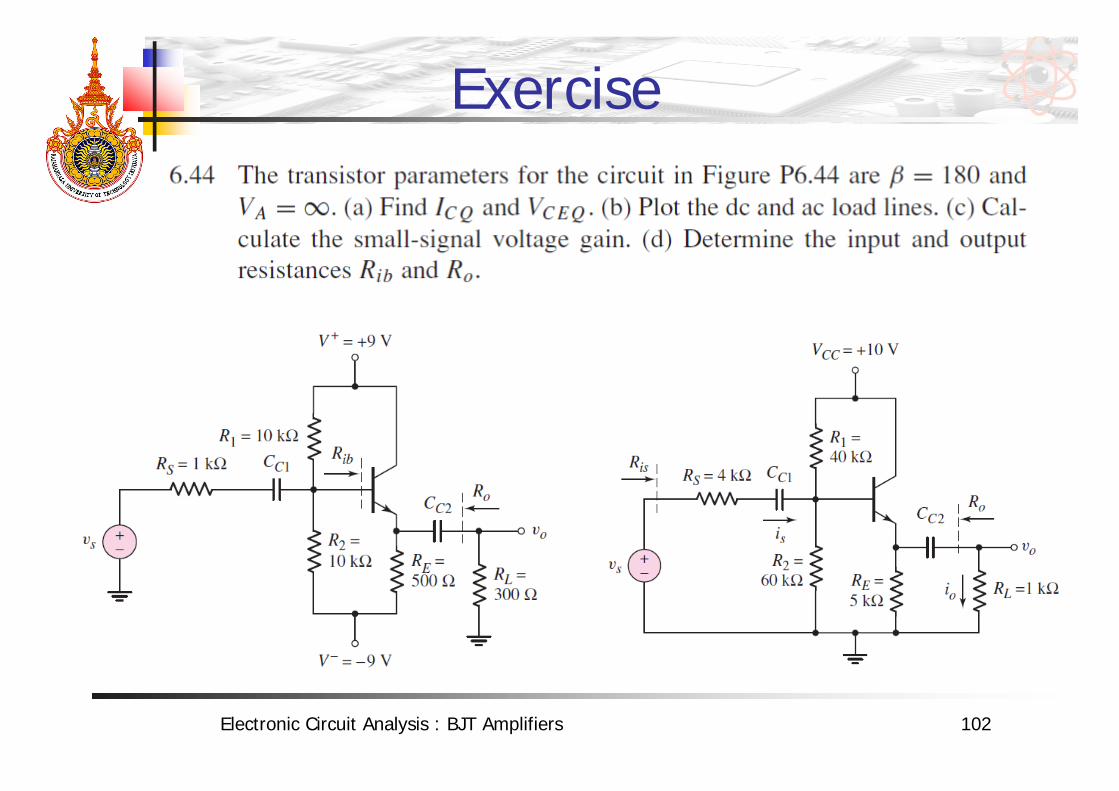
Exercise
Electronic Circuit Analysis : BJT Amplifiers 102


![EKT104 ANALOG ELECTRONIC CIRCUITS [LITAR ELEKTRONIK ANALOG] BASIC BJT AMPLIFIER (PART II) 1 DR NIK ADILAH HANIN BINTI ZAHRI adilahhanin@unimap.edu.my](https://img.pdfslide.tips/doc/110x75/56649ec75503460f94bd3d2c/ekt104-analog-electronic-circuits-litar-elektronik-analog-basic-bjt-amplifier.jpg)


![10.BJT(4).ppt [호환 모드]contents.kocw.net/KOCW/document/2015/korea_sejong/... · 2016-09-09 · Biasing in BJT Amplifier Circuits The classical Discrete Circuit Bias Arrangement](https://img.pdfslide.tips/doc/110x75/5eb5bcb90a92dc485243dd60/10bjt4ppt-eeoe-2016-09-09-biasing-in-bjt-amplifier-circuits-the.jpg)