Embed Size (px)
Citation preview

4.5 µµµµm Pixel Pitch 154 ke- Full Well Capacity CMOS Image Sensor
Koichi Mizobuchi1, Satoru Adachi1, Nana Akahane1, Hirokazu Sawada1, Katsumi Ohta1,
Hiromichi Oshikubo1 and Shigetoshi Sugawa2
1DISP Development, Texas Instruments Japan, 2350 Kihara, Miho-mura, Inashiki-gun, Ibaraki, 300-0496, Japan
Phone: +81-29-880-4066 Fax:+81-29-880-4156 2Gradute School of Engineering, Tohoku University, 6-6-11 Aramaki, Aza-Aoba, Aoba-ku, Sendai, 980-8579, Japan
Phone:+81-22-795-4833 Fax:+81-22-795-4834
E-mail: {mizo, chiro, nana, sawada, ohta, hiromichi-oshikubo}@ti.com, [email protected]
Abstract
A 1/4 inch SVGA format 4.5 µm pixel pitch wide
dynamic range (WDR) CMOS image sensor with
resistance to high temperatures has been developed.
The pixel has been linearly shrunk to 4.5 µm pitch
keeping the same 0.18 µm 2-poly-silicon 3-metal process
technology node and the same 5-transistor 1-photodiode
1-capacitor schematic. The inorganic cap layer to
suppress the degradation of the spectra response of the
on-chip micro lens (OCML) and the color filter at high
temperatures has been also employed. Fourier transform
infrared spectrophotometer (FTIR) has clarified the
chemical aspects of the thermal resistance improvement.
The image sensing performance is compared with the 1/3
inch SVGA format sensor with 5.6 µm pixel pitch. A low
dark temporal noise of 2.3 e-rms is obtained by the
optimization of the readout circuitry (PGA gain: ×2). The
full well capacity (FWC) for 4.5 µm pixel pitch is 154 ke-
and the dynamic range is extended to 96.5 dB with only
-3.5 dB drop from 5.6 µm pixel pitch. The FWC is about
five times as much as the conventional CMOS image
sensor at the same 4.5 µm pixel pitch. The image sample
of the 1/4 inch SVGA format CMOS image shows no
significant degradation in SNR even in dark portion and
bright portion.
Introduction
The CMOS image sensor with lateral overflow
integration capacitor (LOFIC) enables the full well
capacity (FWC) not to be limited by photodiode (PD) or
the floating diffusion (FD) FWC. Fig.1 shows the pixel
pitch dependency of the FWC for the CMOS image
sensor with LOFIC, as compared with conventional
CMOS image sensors reported in the past [1-5]. The
conventional CMOS image sensors show linear decrease
of the FWC with the pixel pitch less than 5 µm. However
the FWC does not increase as the pixel pitch goes over 5
µm. This is because the FWCs, for both cases, are
dominated by the PD FWC and the FD FWC, respectively.
The CMOS image sensor with LOFIC has previously
been shrunk to 5.6 µm pixel pitch and demonstrated
237,000 e- FWC, 2.4 e
-rms temporal noise performance,
and 100 dB dynamic range (DR) [6-8]. However, the pixel
shrink-ability is still concerned because the pixel
schematic includes five transistors, one photodiode and
one capacitor. Security camera applications require 1/3 or
1/4 inch optical size and resolutions with SVGA, SXGA
and full-HD format. The pixel is required to be shrunk to
2.75 µm pitch and beyond in the future. In order to
breakthrough this issue, various approaches including
process technology node, pixel structure and pixel circuit
changes are taken into consideration. In this paper, the
pixel has been linearly shrunk to 4.5 µm pitch keeping the
same process technology node and the same schematic, a
1/4 inch SVGA format CMOS image sensor has been
fabricated and its image quality has been evaluated. In
order to assure the temperature resistance up to 85 ˚C, the
inorganic cap layer onto organic micro lens in the
previous generation is taken over. The chemistry of the
prevention of the thermal decomposition is analyzed in
more detail.
1
10
100
1000
0 2 4 6 8 10 12
Pixel Pitch [µm]
Full Well Capacity (FWC) [Ke- ]
FD FWC dominated
PD FWC dominated
This work:
4.5 µm
LOFIC
Conventional
1
10
100
1000
0 2 4 6 8 10 12
Pixel Pitch [µm]
Full Well Capacity (FWC) [Ke- ]
FD FWC dominated
PD FWC dominated
This work:
4.5 µm
LOFIC
Conventional
Fig.1 Pixel pitch vs full well capacity for LOFIC and
conventional CMOS image sensors.

Pixel Schematic and Block Diagram
Fig.2 shows the pixel schematic and the operation
diagram. The pixel schematic consists of a fully
depleted photodiode (PD), a floating diffusion to
convert the charge to the voltage (FD), a charge
transfer switch (M1), an lateral over-flow integration
capacitor (LOFIC), a switch between the FD and the
LOFIC (M3), a reset switch (M2), a pixel source
follower (M4) and a pixel select switch (M5). The
basic concept in this pixel circuit is to use the switch
M1 for a suitable overflow path of saturated
photoelectrons and integrate overflowed photoelectrons
in the FD and the LOFIC during a charge integration
period.
The non-saturated photoelectrons are transferred from
the PD to the FD and converted to the voltage as a high
sensitivity low light signal (S1). The dynamic range is
extended by fully utilizing the photoelectrons
overflowed from the PD, integrated at the FD+LOFIC
and converted to the voltage as a bright light signal S2.
In the CDS operation, the only N2 in the next frame
(defined as N2’) can be removed by the subtraction of
(S2+N2)-N2’ in the same horizontal blanking period.
φφφφX
φφφφR
φφφφT
PD
M1
M2
M3
LOFIC
M4
M5
FD
φφφφS
φφφφX
φφφφR
φφφφT
PD
M1
M2
M3
LOFIC
M4
M5
FD
φφφφS
(a)
φφφφR
φφφφT
φφφφS
φφφφX
N2N1
S1+N1S2+N2
1H
N2’’’’
φφφφR
φφφφT
φφφφS
φφφφX
N2N1
S1+N1S2+N2
1H
N2’’’’
(b)
Fig.2 Pixel schematic (a) and operation diagram (b) for
CMOS image sensor with LOFIC
Fig.3 shows the block diagram and the packaged chip
micrograph of the 1/4 inch SVGA format 4.5µm pixel
pitch wide dynamic range (WDR) CMOS image sensor.
In the readout circuitry, the kT/C noise at the analog
memory capacitance and the horizontal line capacitance
are kept as small as possible. A continuous capacitive
feedback programmable gain amplifier (PGA) with ×1, 2,
4 or 8 gain is introduced in the sensor to eliminate kT/C
noise in contrast to the switched capacitor PGA having
kT/C noise as a primary contributor. The noise calculation
of the readout circuitry results in 1.7 e-rms (PGA gain: ×2).
The sensor chips are fabricated through 0.18 µm
2-poly-silicon 3-metal process with the very low dark
current FEOL and BEOL implementation [7, 8]. The
LOFIC is formed by a stacked poly-silicones structure.
RGB Bayer color filters and on-chip micro lenses with the
temperature resistant inorganic cap layer are also formed.
Pixel Array :
1/4”SVGA (800x600 pixels)
4.5 µm Pixel Pitch
Vertical Shift Register
Horizontal Shift Register 1
Horizontal Shift Register 2
Signal and Noise Hold 2
Signal and Noise Hold 1S=S1
φN2φS2
φH
φV
φSφX
φTφR
φN1φS1
φVSR
φHSR
φHφHSR
S=S2+ 2N2’√√√√
Differential
Amplifier 2
Gain=x1,2,4,8
Differential
Amplifier 1
Gain=x1,2,4,8
Voltage Regulator
(a)
(b)
Fig.3 Block diagram (a) and packaged chip (b) of 1/4 inch SVGA CMOS image sensor with LOFIC.
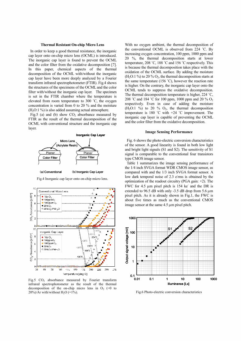
Thermal Resistant On-chip Micro Lens
In order to keep a good thermal resistance, the inorganic
cap layer onto on-chip micro lens (OCML) is introduced.
The inorganic cap layer is found to prevent the OCML
and the color filter from the oxidative decomposition [7].
In this paper, chemical aspects of the thermal
decomposition of the OCML with/without the inorganic
cap layer have been more deeply analyzed by a Fourier
transform infrared spectrophotometer (FTIR). Fig.4 shows
the structures of the specimens of the OCML and the color
filter with/without the inorganic cap layer. The specimen
is set in the FTIR chamber where the temperature is
elevated from room temperature to 300 ˚C, the oxygen
concentration is varied from 0 to 20 % and the moisture
(H2O:1 %) is also added assuming actual atmosphere.
Fig.5 (a) and (b) show CO2 absorbance measured by
FTIR as the result of the thermal decomposition of the
OCML with conventional structure and the inorganic cap
layer.
(a)Conventional (b)Inorganic Cap Layer
Planer
Inorganic Cap Layer
Planer
Micro Lens
(Acrylate Resin)
Color Filter Color Filter
(a)Conventional (b)Inorganic Cap Layer
Planer
Inorganic Cap Layer
Planer
Micro Lens
(Acrylate Resin)
Color Filter Color Filter
Fig.4 Inorganic cap layer onto on-chip micro lens.
Fig.5 CO2 absorbance measured by Fourier transform
infrared spectrophotometer as the result of the thermal
decomposition of the on-chip micro lens in O2 (=0 to
20%)/Ar with/without H2O (=1%).
With no oxygen ambient, the thermal decomposition of
the conventional OCML is observed from 224 ˚C. By
increasing oxygen concentration, 100 ppm, 1000 ppm and
20 %, the thermal decomposition starts at lower
temperature, 208 ˚C, 188 ˚C and 156 ˚C respectively. This
is because the thermal decomposition takes place with the
oxidation of the OCML surface. By adding the moisture
(H2O:1 %) to 20 % O2, the thermal decomposition starts at
the same temperature (156 ˚C), however the reaction rate
is higher. On the contrary, the inorganic cap layer onto the
OCML tends to suppress the oxidative decomposition.
The thermal decomposition temperature is higher, 224 ˚C,
208 ˚C and 184 ˚C for 100 ppm, 1000 ppm and 20 % O2
respectively. Even in case of adding the moisture
(H2O:1 %) to 20 % O2, the thermal decomposition
temperature is 180 ˚C with +24 ˚C improvement. The
inorganic cap layer is capable of preventing the OCML
and the color filter from the oxidative decomposition.
Image Sensing Performance
Fig. 6 shows the photo-electric conversion characteristics
of the sensor. A good linearity is found in both low light
and bright light signals (S1 and S2). The sensitivity of S1
signal is comparable to the conventional four transistors
type CMOS image sensor.
Table 1 summarizes the image sensing performance of
the 1/4 inch SVGA format WDR CMOS image sensor, as
compared with and the 1/3 inch SVGA format sensor. A
low dark temporal noise of 2.3 e-rms is obtained by the
optimization of the readout circuitry (PGA gain: ×2). The
FWC for 4.5 µm pixel pitch is 154 ke- and the DR is
extended to 96.5 dB with only -3.5 dB drop from 5.6 µm
pixel pitch. As it is already shown in Fig.1, the FWC is
about five times as much as the conventional CMOS
image sensor at the same 4.5 µm pixel pitch.
0.1
1
10
100
1000
0.01 0.1 1 10 100 1000
Illuminance [Lx]
Output signal voltage [mV]
S1 S2
0.1
1
10
100
1000
0.01 0.1 1 10 100 1000
Illuminance [Lx]
Output signal voltage [mV]
0.1
1
10
100
1000
0.01 0.1 1 10 100 1000
Illuminance [Lx]
Output signal voltage [mV]
S1 S2
Fig.6 Photo-electric conversion characteristics

Fig.7 shows image samples captured by both the 1/4 inch
and the 1/3 inch SVGA format WDR CMOS image
sensors with LOFIC. No significant degradation in SNR is
observed even in dark portion and bright portion. The
fabricated sensor chips are expected to fulfill promising
performance capturing dark and bright mixed scenes
required to security camera applications.
Conclusion
A 1/4 inch SVGA format 4.5 µm pixel pitch wide
dynamic range (WDR) CMOS image sensor with
resistance to high temperatures has been developed.
The pixel has been linearly shrunk keeping the same
process technology node and the same schematic. The
inorganic cap layer to suppress the degradation of the
spectra response of the on-chip micro lens (OCML)
and the color filter at high temperatures has been also
employed. The image sensing performance is compared
with the 1/3 inch SVGA format sensor with 5.6 µm pixel
pitch. A low dark temporal noise of 2.3 e-rms is obtained
by the optimization of the readout circuitry (PGA gain:
×2). The full well capacity (FWC) for 4.5 µm pixel pitch
is 154 ke- and the dynamic range is extended to 96.5 dB
with only -3.5 dB drop from 5.6 µm pixel pitch. The FWC
is about five times as much as the conventional CMOS
image sensor at the same 4.5 µm pixel pitch. The image
sample of the 1/4 inch SVGA format CMOS image shows
no significant degradation in SNR even in dark portion
and bright portion.
References
[1] G. Agranov et al, Proc. 2005 IEEE Workshop on CCDs
and AISs, pp.206-209 (2005)
[2] G. Meynants et al, Proc. 2005 IEEE Workshop on CCD
and AISs, pp.246-249 (2005)
[3] R.Aerts et al, Proc. 2007 International Image Sensor
Workshop, pp.74-77 (2007) [4] A. Krymski, Proc. 2007 International Image Sensor
Workshop, pp.78-81 (2007)
[5] X. Liu and et al, Proc. 2007 International Image Sensor
Workshop, pp.327-330 (2007) [6] S. Sugawa et al., 2005 ISSCC Dig. Tech. Papers,
pp.352-353 (2005)
[7] K. Mizobuchi, S.Sugawa et al, Proc. 2007 International Image Sensor Workshop, pp.26-29 (2007)
[8] K. Mizobuchi, S.Sugawa et al, Proc. 2008 Electronic
Imaging Science and Technology, pp.618604-1-4 (2008)
Table 1 Image sensing performance comparison between 1/4
inch (a) and 1/3 inch (b) WDR CMOS image sensors
0.18µm 2P3M CMOS0.18µm 2P3M CMOSProcess technology
Previous workThis work
96.5 dB
154 Ke-
750 mV
770 mV
0.19 mVrms
(2.3 e-rms)
x1, 2, 4, 8
60 fps
5 V
4.5 µm
800 × 600
1/4 inch
237 Ke-Full well capacity
x1, 2, 4, 8Differential amplifier gain
100 dBDynamic range
870 mVSaturation of S2(Gain=x1)
990 mVSaturation of S1 (Gain=x2)
0.20 mVrms
(2.4 e-rms)
Temporal noise (Gain=x2)
60 fpsFrame rate
5 VOperation voltage
800 × 600Effective number of pixels
1/3 inchOptical format
5.6 µmPixel pitch
(a)
(b)
Fig.7 Image samples captured by 1/4 inch (a) and 1/3 inch (b)
WDR CMOS image sensors
![C) Masanori Doi Nobuya Sugawa Y 7 T VCNL 17 < B ] TV ... · C) Masanori Doi Nobuya Sugawa Y 7 T VCNL 17 < B ] TV. > Yamaha SymPhonic Band band/ YAMAHA A. S / Alan Menken](https://img.pdfslide.tips/doc/110x75/5e88189ffcc51e631471eb91/c-masanori-doi-nobuya-sugawa-y-7-t-vcnl-17-b-tv-c-masanori-doi-nobuya.jpg)