Embed Size (px)
Citation preview

저 시-비 리- 경 지 2.0 한민
는 아래 조건 르는 경 에 한하여 게
l 저 물 복제, 포, 전송, 전시, 공연 송할 수 습니다.
다 과 같 조건 라야 합니다:
l 하는, 저 물 나 포 경 , 저 물에 적 된 허락조건 명확하게 나타내어야 합니다.
l 저 터 허가를 면 러한 조건들 적 되지 않습니다.
저 에 른 리는 내 에 하여 향 지 않습니다.
것 허락규약(Legal Code) 해하 쉽게 약한 것 니다.
Disclaimer
저 시. 하는 원저 를 시하여야 합니다.
비 리. 하는 저 물 리 목적 할 수 없습니다.
경 지. 하는 저 물 개 , 형 또는 가공할 수 없습니다.

77-GHz Waveform Generator withMultiple Frequency Shift Keying forMulti-Target Detection Automotive
Radar Applications
Nguyen Ngoc Quang
Department of Electrical Engineering
2015
Ulsan National Institute of Science andTechnology
Master Thesis
77-GHz Waveform Generator withMultiple Frequency Shift Keying forMulti-Target Detection Automotive
Radar Applications
Author
Nguyen Ngoc Quang
A thesis submitted to the School of Electrical and Computer Engineering
and the Graduate School of UNIST
in partial fulfilment of the requirements for the degree of
Master of Science
06.19.2015
Approved by
Major Advisor
Dr. Franklin Bien

77-GHz Waveform Generator withMultiple Frequency Shift Keying forMulti-Target Detection Automotive
Radar Applications
Nguyen Ngoc Quang
This certifies that the thesis of Nguyen Ngoc Quang is approved.
06.19.2015
Thesis Supevisor: Prof. Franklin Bien
Prof. JaeJoon Kim - Thesis Committee Member 1
Prof. Jae-Hyouk Choi - Thesis Committee Member 2

Declaration of Authorship
I, Nguyen Ngoc Quang, declare that this thesis titled, ’77-GHz Waveform Generator
with Multiple Frequency Shift Keying for Multi-Target Detection Automotive Radar
Applications’ and the work presented in it are my own. I confirm that:
� This work was done wholly for research at this University.
� Where any part of this thesis has previously been submitted for a degree or any
other qualification at this University or any other institution, this has been clearly
stated.
� Where I have consulted the published work of others, this is always clearly at-
tributed.
� Where I have quoted from the work of others, the source is always given. With
the exception of such quotations, this thesis is entirely my own work.
� I have acknowledged all main sources of help.
� Where the thesis is based on work done by myself jointly with others, I have made
clear exactly what was done by others and what I have contributed myself.
Signed:
Date:
i

“Your work is going to fill a large part of your life, and the only way to be truly satisfied
is to do what you believe is great work. And the only way to do great work is to love
what you do. If you haven’t found it yet, keep looking. Don’t settle. As with all matters
of the heart, you’ll know when you find it.”
Steve Jobs

ULSAN NATIONAL INSTITUTE OF SCIENCE AND TECHNOLOGY
Abstract
School of Electrical and Computer Engineering
Department of Electrical Engineering
Master of Science
77-GHz Waveform Generator with Multiple Frequency Shift Keying for
Multi-Target Detection Automotive Radar Applications
by Nguyen Ngoc Quang
In automotive radar applications, the modulation waveform plays an important role
in detecting multiple targets. Two well-known continuous waves in the literature are
Frequency Modulated Continuous Wave (FMCW) and Frequency Shift Keying (FSK).
These two waveforms basically fulfil the requirements of automotive radars. However,
two modulations have limitations in multiple target situations. The ghost targets are
introduced in FMCW radars, thus two or more measurement cycles are expanded to
resolve the target ambiguities. In contrast to that FSK cannot solve targets in range
direction. For this reason, the combination of FMCW and FSK was proposed, called
MFSK. This waveform shows good performance, with a high range and velocity resolu-
tion, short measurement time, and ability to avoid ghost targets. The main drawback of
this modulation is the complexity. In this thesis, all the perspectives about MFSK mod-
ulation waveform from basic fundamentals to hardware implementation are presented.
In addition, the proposed MFSK waveform generator for automotive radar system is
elaborated to improve the target detections and shorter measurement time.. . .

Acknowledgements
Foremost, I would like to express my sincere gratitude to my advisor, Prof. Franklin
Bien, for the continuous support of my M.S study and research, for his patience, moti-
vation, enthusiasm, and immense knowledge. His guidance helped me in all the time of
research and writing of this thesis. I could have imagined having a better advisor and
mentor for my M.S study.
Besides my advisor, I would like to thank the rest of my thesis comittee: Prof. Jae-Joon
Kim and Prof. Jae-Hyouk Choi for their encouragement, insightful comments, and valu-
able advices.
I thank my fellow labmates in BICDL: Sai Kiran Oruganti, Na KyungMin, Heo SangHyun,
Jang Heedon, Ma HyunGun, Yoo HyonGi, Kim SeulKiRom, Liu Zhenyi, Song Joohyeb,
and Alka for the stimulating discussions and for all the fun we have had during 2 years.
Also I thank my friends in UNIST.
Last but not the least, I would like to thank my family: my parents Nguyen Van Minh
and Ho Thi Hong Yen, for giving birth to me at the first place and supporting me spir-
itually throughout my life. Also, I really appreciate my fiancee, LyLy, for her patience,
support, and encouragement during my M.S course.
This research was financially supported by the R&D Infrastructure for Green Electric Ve-
hicle (RE-EV) through the Ministry of Trade Industry & Energy and Korea Institute for
Advancement of Technology and by the Ministry of Science, ICT and Future Planning,
Korea, under the Information Technology Research Center support program (NIPA-
2014-(H0301-14-1008)) supervised by the National IT Industry Promotion Agency.. . .
iv

Contents
Declaration of Authorship i
Abstract iii
Acknowledgements iv
List of Figures vii
List of Tables ix
Abbreviations x
1 Introduction 1
1.1 Motivation . . . . . . . . . . . . . . . . . . . . . . . . . . . . . . . . . . . 1
1.2 Modulation Waveform for Multi-target Detection . . . . . . . . . . . . . . 3
1.2.1 Frequency Modulated Continuous Waveform . . . . . . . . . . . . 4
1.2.2 Frequency Shift Keying . . . . . . . . . . . . . . . . . . . . . . . . 6
1.2.3 Multiple Frequency Shift Keying . . . . . . . . . . . . . . . . . . . 7
2 Different Approaches to Generate Modulation Waveform 10
2.1 Diophantine Phase Locked Loops . . . . . . . . . . . . . . . . . . . . . . . 10
2.2 Direct Digital Frequency Synthesizer . . . . . . . . . . . . . . . . . . . . . 12
2.3 Fractional-N Phase Locked Loops . . . . . . . . . . . . . . . . . . . . . . . 15
3 Proposed MFSK Waveform Generator 17
3.1 Proposed MFSK Waveform Generator . . . . . . . . . . . . . . . . . . . . 17
3.2 MFSK Modulation Control Logic . . . . . . . . . . . . . . . . . . . . . . . 22
3.3 MFSK Transceiver Implementation . . . . . . . . . . . . . . . . . . . . . . 23
4 System Performance Results 27
4.1 MFSK Waveform Generator . . . . . . . . . . . . . . . . . . . . . . . . . . 27
4.2 Improvement of Target Detection . . . . . . . . . . . . . . . . . . . . . . . 29
4.3 Discussion . . . . . . . . . . . . . . . . . . . . . . . . . . . . . . . . . . . . 32
5 Future Work and Research 35
v

Contents
6 Summary and Conclusion 38

List of Figures
1.1 Applications of automotive radar systems. . . . . . . . . . . . . . . . . . . 2
1.2 First automotive radar experiment. . . . . . . . . . . . . . . . . . . . . . . 3
1.3 Third generation 77-GHz Long-Range Radar Sensor from Bosch. . . . . . 4
1.4 Frequency Modulated Continuous Waveform principle. . . . . . . . . . . . 5
1.5 a) Single target solution. b) Ghost targets in multi-target situation. . . . 6
1.6 a) Dual FMCW waveform. b) Improvement of target detection by usingDual FMCW. . . . . . . . . . . . . . . . . . . . . . . . . . . . . . . . . . . 6
1.7 Frequency Shift Keying waveform principle. . . . . . . . . . . . . . . . . . 8
1.8 Multiple Frequency Shift Keying waveform principle. . . . . . . . . . . . . 9
2.1 Fundamental approach to generate the modulation waveform. . . . . . . . 11
2.2 A basic PLL in the DFS. . . . . . . . . . . . . . . . . . . . . . . . . . . . 11
2.3 General architecture of DFS. . . . . . . . . . . . . . . . . . . . . . . . . . 12
2.4 DFS-based FMCW waveform generator. . . . . . . . . . . . . . . . . . . . 13
2.5 Block diagram of DDFS. . . . . . . . . . . . . . . . . . . . . . . . . . . . . 14
2.6 DDFS-based FMCW waveform generator. . . . . . . . . . . . . . . . . . . 14
2.7 Low-spec DDFS-based FMCW waveform generator. . . . . . . . . . . . . 15
2.8 Fractional-N-based FMCW waveform generator. . . . . . . . . . . . . . . 16
3.1 Proposed MFSK waveform generator. . . . . . . . . . . . . . . . . . . . . 18
3.2 a) Conventional tri-state PFD. b) Circuit schematic of D flip-flop. . . . . 18
3.3 Concept of gain-boosting circuit. . . . . . . . . . . . . . . . . . . . . . . . 19
3.4 Design of Charge Pump with gain-boosting circuit. . . . . . . . . . . . . . 19
3.5 Design of prescaler. . . . . . . . . . . . . . . . . . . . . . . . . . . . . . . . 20
3.6 a) Divide-by-2/3 cell. b) Embedded AND gate into TSPC latch. . . . . . 21
3.7 16-bit ∆ − Σ modulator. . . . . . . . . . . . . . . . . . . . . . . . . . . . . 22
3.8 Block diagram of proposed MFSK modulation control logic. . . . . . . . . 23
3.9 a) Full Adder circuit. b) Adder/Subtractor circuit . . . . . . . . . . . . . 24
3.10 a) 16-bit comparator. b) Bit-sliced comparator. . . . . . . . . . . . . . . . 25
3.11 Timing diagram of proposed MFSK modulation control logic. . . . . . . . 25
3.12 Hardware implementation a) RF part. b) Baseband part. . . . . . . . . . 26
4.1 Simulation results of proposed architecture. . . . . . . . . . . . . . . . . . 28
4.2 MFSK waveform: Bsw=150 MHz, TCPI=5.12 ms, N=256, Tstep=20 µs,fstep=-294 kHz, finc=588 kHz. . . . . . . . . . . . . . . . . . . . . . . . . 28
4.3 MFSK waveform: Bsw=300 MHz, TCPI=2.56 ms, N=256, Tstep=10 µs,fstep=-588 kHz, finc=1167 kHz. . . . . . . . . . . . . . . . . . . . . . . . . 29
4.4 MFSK waveform: Bsw=150 MHz, TCPI=1.28 ms, N=128, Tstep=10 µs,fstep=-294 kHz, finc=588 kHz. . . . . . . . . . . . . . . . . . . . . . . . . 29
vii

List of Figures
4.5 MFSK waveform: Bsw=225 MHz, TCPI=2.56 ms, N=256, Tstep=10 µs,fstep=-294 kHz, finc=882 kHz. . . . . . . . . . . . . . . . . . . . . . . . . 30
4.6 Two different waveforms: a) MFSK waveform withBsw=150 MHz, TCPI=2.56ms, N=256, fstep= -294 kHz, finc= 588 kHz. b) FMCW waveform withBsw=150 MHz, TCPI=2.56 ms. . . . . . . . . . . . . . . . . . . . . . . . . 31
4.7 a) Spectrogram of FMCW waveform. b) Spectrogram of MFSK waveform. 32
4.8 a) Spectrum of FMCW waveform. b) Spectrum of MFSK waveform. . . . 33
5.1 Principle and signal processing of chirp sequence. . . . . . . . . . . . . . . 36
5.2 Vital sign detection system using MFSK waveform. . . . . . . . . . . . . . 37

List of Tables
4.1 Modeling parameters of the front-end module . . . . . . . . . . . . . . . . 30
4.2 Estimated targets of FMCW and MFSK radars . . . . . . . . . . . . . . . 32
ix

Abbreviations
SRR Short-Range Radar
LRR Long-Range Radar
ABS Anti-Lock Breaking
ESC Electronic Stability Control
ADAS Advanced Driver Assisstant System
ACC Adaptive Cruise Control
BSD Blind Spot Detection
LCA Lane Change Assisstance
CW Continuous Wave
FMCW Frequency Modulated Continuous Wwaveform
FSK Frequency Shift Keying
MFSK Multiple Frequency Shift Keying
PLL Phase Locked Loop
DDFS Direct Digital Frequency Synthesizer
DFS Diophantine Frequency Synthesis
PFD Phase Frequency Detector
CP Charge Pump
LF Loop Filter
MMFD Multi-Modulus Frequency Divider
VCO Voltage Controlled Oscillator
DAC Digital-to-Analog Converter
SPI Serial Peripheral Interface
SSB Single-Sideband Mixer
LUT Look-Up Table
FMCL FMCW Modulation Control Logic
x

Abbreviations
MMCL MFSK Modulation Control Logic
DSM Delta-Sigma Modulator
TSPC True Single-Phase Clock
MMIC Monolithic Microwave Integrated Circuit
UMS United Monolithic Semiconductors
HBT Heterojunction Bipolar Transistor
pHEMT pseudomorphic High-Electron-Mobility-Transistor
CML Common Mode Logic
MASH Multi-stAge noise SHaping
RCA Ripple-Carry Adder
LNA Low Noise Amplifier
NF Noise Figure
LO Local Oscillator
VGA Variable Gain Amplifier
AGC Automatic Gain Control
PDA PLL Design Assistant
RCS Radar Cross Section
FFT Fast Fourier Transform
CFAR Constant False Alarm Rate
SNR Signal Noise Ratio

For Dedicated To My Family and My Fiancee. . .
xii

Chapter 1
Introduction
1.1 Motivation
Nowadays, the radar applications are focused the attention on avoiding the collisions
between automobiles in the traffic conditions. Due to the strong limitations of human
beings in the capability of estimating the distance and the speed between cars, driving
a car remains a risky task [1]. Therefore, an additional driver assistance is needed to
improve the safety and reduce the human error. The driving task would be much safer
with the significant progression of the automotive radar systems. A single automotive
radar sensor has the ability to sense the environment situations.
Automotive radar systems can be categorized into short-range radar (SRR) and long-
range radar (LRR) depending on the coverage distance. Two frequency bands are allo-
cated for automotive applications, 24-29 GHz and 76-81 GHz. Some remarkable auto-
motive applications can be listed: Adaptive Cruise Control (ACC), Blind Spot Detection
(BSD),and Lane Change Assistance (LCA), as shown in Figure 1.1. The sensor is able
to monitor the blind area, detect possible obstacles and then have the suitable reaction
- control the break and the throttle.
Radar system is based on the electromagnetic to detect and estimate the location of
targets [2]. By radiating energy into the free space and detecting the echo signal, the
system can indicate the presence of targets and target information can be calculated as
well. The first radar experiment operating at microwave frequencies took place already
in the 1970s (Figure 1.2). This contributed an important step to the development of
the current automotive radar systems. In order to improve the safety, the Anti-Lock
Breaking (ABS) system, Electronic Stability Control (ESC), and an powerful Advanced
Driver Assistant System (ADAS) are equipped onto the moder cars. In comparison
to other sensors, the advantages of automotive radar sensor are all-weather capability
1

Chapter 1. Introduction
Figure 1.1: Applications of automotive radar systems.
and the accurate target measurement, that makes it become a strong candidate for the
ADAS.
Accompanied by the considerable improvement in microwave semiconductors, digital
signal processing units and functionality of the micro-controllers, the automotive radar
is commercialized in the late 1990s. Figure 1.3 depicts a 77-GHz commercial radar sen-
sor using cost-effective SiGe technology. This radar sensor can detect multiple targets
at the distance up to 250 m and the horizontal opening angle is 300. The dimensions of
this radar sensor (HxWxD) with the embedded antennas is 77mmx74mmx58mm. The
success of radar technology in the commercial market is due to the substantial low cost,
compact size and all-weather conditions.
The essential requirement of automotive applications is detecting all targets, range R
and radial velocity vr, in the local environment of traffic, even in multi-target cases.
The target information, range and radial velocity, should be measured simultaneously,
unambiguously and precisely by the radar sensor. There would be several targets, pedes-
trians and vehicles, in the observation area and all targets have to be detected by the
radar sensor including fixed targets. Thus, the multi-target detection ability is one of
the most important requirements of a radar sensor. Beside the high hardware quality,
the modulation waveform plays an important role in this application. This task is a
continuing technical challenge in automotive applications. In the last decade, the re-
markable progress in the development of radar sensors is marked by the presentation
of fully integrated 77-GHz radar on an single chip based on CMOS technology [3, 4].
This results in the significant reduction of product costs and increase of the accuracy in
measurement.
2

Chapter 1. Introduction
Figure 1.2: First automotive radar experiment.
1.2 Modulation Waveform for Multi-target Detection
In general, the CW radar system continuously transmits a modulated sinusoidal signal
with frequency fT . The reflected signal, frequency fR, is down-converted into the base-
band, and the frequency difference is called beat frequency fB. Depend on the waveform,
this beat frequency contains information of targets through the propagation delay and
the Doppler frequency.
Basically, the target range R depends on the two-way propagation delay τ and can be
estimated as
τ =2R
c(1.1)
where c is the speed of light.
In case of non-stationary target, there is a frequency shift, called Doppler frequency fD.
The relation between the radial velocity vr of moving target and the Doppler frequency
can be expressed as
fD = − 2
λvr (1.2)
where λ is the wavelength.
3

Chapter 1. Introduction
Dimensions (HxWxD): 77mmx74mmx58mm
Figure 1.3: Third generation 77-GHz Long-Range Radar Sensor from Bosch.
1.2.1 Frequency Modulated Continuous Waveform
Essentially, the unmodulated waveform has ability to measure the radial velocity, but
it has the limitation in range measurement. Thus, this waveform cannot fulfil the per-
formance requirement of automotive applications, especially in multi-target situations.
The linear frequency modulated continuous waveform (FMCW) can succeed in estimat-
ing the target range R and radial velocity vr, even in multiple target cases [5].
Figure 1.4 depicts the principle of FMCW waveform. The frequency of transmitted sig-
nal is linearly modulated in a chirp time. This waveform consists of a up-chirp and a
down-chirp, which indicate the positive and negative slope. These two sweeps have the
same bandwidth and gradient slope.
In moving target situation, the beat frequency fB includes two components, the fre-
quency shift fτ contains target range information and the Doppler frequency fD holds
the radial velocity information. Consequently, the target range and radial velocity can-
not be unambiguously resolved by an single up-chirp signal. Thus, the extended chirp
is needed with negative sweep to avoid this ambiguity. There are two beat frequencies
fB,1 and fB,2 corresponding to up- and down-chirp signals. In this case, the target
4

Chapter 1. Introduction
TCPI
Bsw
TCPIt
fT(t)
fB,u fB,d
Down-convert
f(t)
t
FFT FFT
fB,u
fB,d
vr,R
Transmitted signal
Received signal
Figure 1.4: Frequency Modulated Continuous Waveform principle.
parameters can be estimated by two linear equations
fB,u = fD + fτ = − 2
λvr −
2
c
BswTCPI
R (1.3a)
fB,d = fD − fτ = − 2
λvr +
2
c
BswTCPI
R (1.3b)
where Bsw is the modulation bandwidth and TCPI is the coherent processing interval.
The intersection point of these two equations can be represented in the range-velocity
plane, as shown in Figure 1.5-a. Assuming that there is a single target, solving the
linear equations provides an unambiguous solution. In case of two targets, there are two
beat frequencies for each up- and down-chirp signal. There are four intersection points
can be found by the graphical solution. It means there are two real targets and two
un-real targets, called ghost targets (see Figure 1.5-b). This problem is caused by the
association between the beat frequencies of up- and down-chirp, there is no chance to
5

Chapter 1. Introduction
R
vrUp-chirp
Down-chirp
Target
R
vrUp-chirp
Down-chirp
Target?
?
?
?
a) b)
Figure 1.5: a) Single target solution. b) Ghost targets in multi-target situation.
R
vr Up-chirp 1
Down-chirp 1
TCPI1
Bsw
TCPI1t
fT(t)
fB,u1
fB,d1
TCPI2TCPI2
fB,u2
fB,d2 Up-chirp 2
Down-chirp 2
a) b)
Transmitted signal
Received signal
Figure 1.6: a) Dual FMCW waveform. b) Improvement of target detection by usingDual FMCW.
find the correct beat frequency pairs.
In order to avoid the ghost targets, additional chirps are needed to make the indication
between the beat frequencies. Figure 1.6-a illustrates the solution of FMCW signal for
multi-target situations. A real target will be the intersection of four beat frequencies
in the range-velocity plane, as shown in Figure 1.6-b. Other targets, which are the
intersections of two or three beat frequencies, are considered as ghost targets. In other
words, the FMCW radars cannot completely succeed in unambiguously measuring target
range and radial velocity in multi-target scenarios.
1.2.2 Frequency Shift Keying
The FMCW waveform is able to simultaneously measure the target range R and radial
velocity vr. Nevertheless, this modulation scheme shows the unambiguities in multiple
target cases, thus an additional time is required to fulfil the requirement of automotive
applications. The ghost targets are presented due to the association between two chirps.
In order to avoid it, the phase is estimated instead of the beat frequency. Therefore, the
Frequency Shift Keying (FSK) waveform is proposed to resolve the problem of FMCW.
The FSK waveform principle is illustrated in Figure 1.7. Two signals are shifted by
6

Chapter 1. Introduction
a small frequency difference, fstep. In a interval time of Tstep, these two frequencies
are transmitted in a intertwined way. The received signals are down-converted into the
baseband, which have the same beat frequency as
fB = fD = − 2
λvr (1.4)
The information of target range R can be estimated from the phase difference of the two
intertwined frequencies
∆φ = 2πfstep2
cR (1.5)
In multi-target situations, if the targets have different speeds, these targets can be
detected by their Doppler frequencies. In other words, the measurement is unambiguous
even in multi-target situations. However, if two targets have the same beat frequency,
it means these targets have the same relative velocity to the automotive radar, then the
range estimation is meaningless. Due to this limitation, this system cannot differentiate
fixed target along the road. This disadvantage limits the use of FSK in automotive
radars.
1.2.3 Multiple Frequency Shift Keying
The FMCW and FSK waveforms basically succeed in measuring target parameters of
automotive radar applications. However, both waveforms exhibit the limitations in
multi-target situations, ghost targets in FMCW radars and targets in range direction
in FSK radars. In order to achieve the advantage of FMCW and FSK modulation, the
combination of two waveforms, called Multiple Frequency Shift Keying (MFSK), is pro-
posed [6]. MFSK waveform can improve the detection ability of the radar system, even
in multi-target scenarios. This waveform shows the high range and velocity resolution
with a short measurement time.
The transmitted signal consists of two linear frequency modulated signals, which is trans-
mitted in an intertwined way like FSK modulation. Two stepwise chirps are shifted by
a small frequency difference as shown in Figure 1.8. The beat frequencies of both base-
band signals have the same value and depend on the target range R and radial velocity
vr, similar to FMCW waveform.
fB = − 2
λvr −
2
c
BswTCPI
R (1.6)
The phase difference is influenced not only by the range as FSK case but also by the
radial velocity of the target. This dependence can be expressed as
∆φ = 2π
(Tstep
2
λvr − fstep
2
cR
)(1.7)
7

Chapter 1. Introduction
Tstep
TCPIt
fT(t)
fB
fstep
Down-convert
f(t)
t
FFT FFT
fB
vr,R
Transmitted signal
Received signal
Figure 1.7: Frequency Shift Keying waveform principle.
where Tstep is the time step and fstep is the frequency step.
Differ from the FMCW scheme, there is no associated task to resolve target information
in the MFSK case. The target parameters can be estimated by solving these two linear
equations. In the Rohling papers [7]-[8], the efficiency of this modulation is demonstrated
by the experimental results. In addition, the target range and relative velocity of cars
or pedestrians can be estimated simultaneously even in multiple target cases, where all
the ghost targets can be completely removed.
8

Chapter 1. Introduction
Tstep
Bsw
TCPIt
fT(t)
fBfstep
Down-convert
f(t)
t
FFT FFT
fB
vr,R
Transmitted signal
Received signal
Figure 1.8: Multiple Frequency Shift Keying waveform principle.
9

Chapter 2
Different Approaches to Generate
Modulation Waveform
Currently, the FMCW waveform is widely applied in the market but the limitations
of this modulation in multi-target scenarios cannot be completely avoided. There are
tremendous improvements in radar applications, several methods have been proposed
to generate the modulation signal. Various circuit techniques can be implemented to
generate the modulation signal [9]. A fundamental idea is to apply a suitable control
voltage to the input of a Voltage-Controlled Oscillator (VCO), as shown in Figure 2.1. In
case of linear voltage-frequency characteristic of the VCO, the output frequency will be
modulated followed the input voltage. For Continuous Wave (CW) radars, the system
requires a large frequency bandwidth for good range resolution but the VCO usually
reveals the non-linear tuning curve. Moreover, the center frequency of a free-running
VCO without feedback loop cannot be fixed due to the temperature drift [10]. In the
receiver chain, the unpredictable center frequency may cause the error in the signal pro-
cessing part. A look-up table or delay line is employed to compensate the non-linearity
of VCO. A Phase-Locked Loop (PLL) incorporates the VCO, compensates the VCO
non-linearity by feedback technique, thus the output frequency can be stabilized. The
modulation signal can be realized by generating the digital code using a Direct Digital
Frequency Synthesizer (DDFS). This chapter discusses several methods to generate the
FMCW modulation waveform.
2.1 Diophantine Phase Locked Loops
In the MFSK modulation scheme, the generator has the capability of shifting the output
frequency with a small step size. Moreover, the lock time should be as small as possible
10

Chapter 2. Different Approaches to Generate Modulation Waveform
VCO
waveform generator
v
t
f
t
Figure 2.1: Fundamental approach to generate the modulation waveform.
fin ÷Ri PFD CP LF fout
÷Ni
VCO
To other loops
Figure 2.2: A basic PLL in the DFS.
to minimize the overshoot while switching frequencies. The Diophantine Frequency
Synthesis (DFS) is one of the solutions that can provide a fine frequency step while
ensuring fast frequency hopping. The idea behind the DFS is based on mathematical
properties of integer numbers and linear Diophantine equations [11, 12].
A DFS consists of two or more basic PLLs, in which the PLLs is fed by a same reference
frequency. An integer-N PLL is adopted in DFS, as shown in Figure 2.2. The first
divider, divider Ri, has a fixed size of Ri. The main prescaler has the variable size,
its size involves a variable part and a fixed value. The variable part can be negative
or positive in a specific range. The output frequency of DFS is the product of mixing
output frequencies of PLLs, adding or subtracting two or more frequencies.
In case of single PLL, the frequency step is equal to the reference input of the Phase
Frequency Detector (PFD), fin/Ri. A small frequency step can be achieved by using
a large divide value of Ri and/or small reference input fin. This leads to low phase
detection frequency, thus a narrow loop bandwidth. However, a PLL with a small loop
bandwidth has limitation in frequency hopping and possibly spurious signals. The trade-
off between the frequency step and high bandwidth can be relaxed by a DFS [12, 13].
DFS allows the frequency shift can be made arbitrarily small with a reasonable divider
and small reference frequency. By using two or more PLLs, the frequency resolution of
11

Chapter 2. Different Approaches to Generate Modulation Waveform
fin fout
…
PFD CP LF÷R1
÷N1
PFD CP LF÷R2
÷N2
PFD CP LF÷Rk
÷Nk
…
VCO
VCO
VCO …
Figure 2.3: General architecture of DFS.
the DFS is distributed. Figure 2.3 shows the general architecture of DFS. A very fine
frequency resolution up to fin/N1N2...Nk can be achieved by combining k PLLs.
In order to generate the modulation waveform, the variable part of the prescaler will be
programmed. Since the variable part can take positive or negative value, the direction
of the modulation sweep can be controlled. A Controller is employed to control the
division ratio of dividers, modulate the output frequency, as illustrated in Figure 2.4.
The more dividers, the more complexity of the Controller is required. Furthermore, the
modulation waveform can affect the complexity of the DFS-based waveform generator.
Moderate loop bandwidth and high resolution are the advantages of this structure.
However, this method exhibits several drawbacks. Firstly, a complex Controller controls
multiple dividers. Secondly, the mixers and frequency synthesizers consume high power.
Moreover, bandpass filters are needed to select suitable output frequency.
2.2 Direct Digital Frequency Synthesizer
Direct Digital Frequency Synthesizer (DDFS) is a method that generates the sinusoidal
waveform by creating a signal in digital domain and converting to analog using a Digital-
to-Analog Converter (DAC). Since the device operates in digital form, it can exhibit
12

Chapter 2. Different Approaches to Generate Modulation Waveform
fin fout
…
PFD CP LF÷R1
÷N1
PFD CP LF÷R2
÷N2
PFD CP LF÷Rk
÷Nk
…
VCO
VCO
VCO …
ControllerFMCW
generator
Figure 2.4: DFS-based FMCW waveform generator.
advantages: fast frequency hopping, fine frequency resolution, and wide bandwidth op-
eration. The DDFS has the posibility of generating various modulation waveform by
programming the control code in digital form through a high speed Serial Peripheral-
Interface (SPI).
The block diagram of DDFS is represented in Figure 2.5. It includes 3 main components:
a phase accumulator, a phase-to-amplitude conversion (or Look-Up Table (LUT)), and
a DAC. The output frequency is determined by two inputs, system clock fclk and the
tuning word M. The phase accumulator reads the binary number from tuning word,
then computes the corresponding phase for the look-up table. The DAC converts that
number to suitable voltage.
Since the DDFS is compatible and can be integrated in CMOS technology, the use of a
DDFS generating the modulated reference signal for a PLL exhibits a suitable approach.
Figure 2.6 depicts the applications of DDFS in automotive radars [14, 15, 16]. The PFD
detects the difference of phase and/or frequency between the reference signal and the
feedback signal. Dependent of this difference, the suitable link or source current will
be provided by the Charge Pump (CP). Then, the Loop Filter (LF) is a low-pass filter
13

Chapter 2. Different Approaches to Generate Modulation Waveform
PHASE-TO-
AMPLITUDE
CONVERTERfout∑
PHASE
ACCUMULATOR
D/A
CONVERTER
PHASE
REGISTER
14 TO
16 BITS
24 TO
48 BITS
SYSTEM
CLOCK
TUNING
WORD M
Figure 2.5: Block diagram of DDFS.
CPDDFS LF
VCO
PFD
Integer-N PLL
fref
÷N
Output
fout
FMCW
generator
Figure 2.6: DDFS-based FMCW waveform generator.
and filters out high-frequency components. The high-frequency output will be down-
converted by the Divider (÷N), then sent to the PFD for comparison. The prescaler
is fixed to a constant value, thus the PLL synthesizes the reference frequency. In this
case, the input frequency is modulated by DDFS instead of constant reference, then the
output always keep track of the change of the modulation input.
By using a low-speed and low-resolution DDFS, the power consumption can be signif-
icantly reduced. The sampling rate of DDFS clock has to be twice times the maximum
frequency to be synthesized, thus it is mandatory of up-converting the DDFS output
frequency to the proper frequency band of automotive radars. This conversion can be
realized by a Single-Sideband Mixer (SSB), a frequency multiplier or by setting DDFS
as the reference input of a integer-N PLL [10]. Because of the flexibility in generating
variety of modulation signal, the DDFS becomes a common choice in the automotive
radar sensor. The FMCW waveform generator based on the low-spec DDFS is depicted
in Figure 2.7.
The main drawbacks that limit the use of this frequency synthesis are the high power
consumption and occupied area. For high-speed and high-resolution DDFS, the power
consumption and area are up to 100 mW and 1 mm2 for the DAC and LUT table [10].
Because of the continual improvements in process and technology, variety of analog
waveform with high resolution and accuracy can be generated by a single DDFS chip.
Nevertheless, due to the limitation of LUT size, the truncation in the DDFS may cause
14

Chapter 2. Different Approaches to Generate Modulation Waveform
CPDDFS LF
VCO
PFD
Integer-N PLL
fref
÷N
Output
fout
FMCW
generator
XO
SSB
Mixer
Figure 2.7: Low-spec DDFS-based FMCW waveform generator.
large frequency error. In addition, the use of integer-N PLL limits the lock time and
may cause the frequency error.
2.3 Fractional-N Phase Locked Loops
Typically, the frequency shift using a integer-N PLL cannot be small due to the trade-off
between the frequency resolution and the loop bandwidth. For that reason, a fractional-
N PLL is adopted for synthesizing the modulation waveform. It has capability of gen-
erating frequency step smaller than reference frequency. In [3, 4, 17, 18, 19, 20, 21, 22],
these designs employs a fractional-N frequency synthesizer operating at 77 GHz. The
output frequency is divided into lower frequency band by a high-speed divider. A Multi-
Modulus Frequency Divider (MMFD) is programmed to control the division ratio, thus
modulates the output frequency of the PLL.
Figure 2.8 shows the block diagram of FMCW waveform generator that recently pre-
sented [3, 4]. Depend on the modulation waveform, the suitable Modulation Control
Logic is designed. In this case, a FMCW Modulation Control Logic (FMCL) is pre-
sented, which can provide the control code of FMCW waveform in digital form. This
control code is modulated by a ∆−Σ Modulator (DSM), then feeds to the MMFD. Differ
from the DDFS-based FMCW waveform generator, the reference frequency is fixed, but
the divide modulus is programmed.
The reference source is compared with the divided signal by a PFD. The phase dif-
ference results in the sink or source current of the Charge Pump (CP). This generates
the control voltage for the Voltage-Controlled Oscillator (VCO) through a Loop Filter
(LF). In this approach, the divider is programmed by the Modulation Control Logic.
The quantization noise will be introduced because of the rapid variation of the division
ratio. This noise will be added into the total phase noise of the PLL. Thus, this noise
needs to be shaped.
15

Chapter 2. Different Approaches to Generate Modulation Waveform
CP
FMCL
LF
VCO
PFD
Fractional-N PLL
fref
÷N
Output
fout
FMCW
generator
DSM
Figure 2.8: Fractional-N-based FMCW waveform generator.
The advantage of this approach is the lower power consumption by entirely removed the
dependence on the DDFS. The Modulation Control Logic is pure digital block, can be
easily integrated into the transceiver for high integration. The average frequency would
be high accurate because of the low-pass behavior of the PLL. Moreover, the fractional-
N PLL offers fast lock time, high resolution. In comparison with the DDFS-based, this
structure exhibits better performance, which is significant power and area saving with
lower frequency error. This architecture provides a promising solution, which is able to
generate a variety of modulation waveform, for future automotive applications.
16

Chapter 3
Proposed MFSK Waveform
Generator
In the Chapter 2, several methods generating modulation waveform were discussed.
Among these 3 approaches, the last method offers some advantages: ability of fully
integrated in CMOS technology, flexible in changing the modulation waveform and low
power consumption. To take the advantages of this method, a fractional-N PLL is
designed for generating MFSK modulation waveform. A MFSK Modulation Control
Logic (MMCL) is introduced, it provides the control code to the DSM. The details of
circuit implementation will be discussed in this Chapter.
3.1 Proposed MFSK Waveform Generator
The proposed waveform generator is based on a fractional-N PLL incorporating a MFSK
Modulation Control Logic (MMCL). Figure 3.1 depicts the block diagram of the pro-
posed waveform generator. The PLL consists of a Phase Frequency Detector (PFD),
Charge Pump (CP), Loop Filter (LF), and the Multi-Modulus Frequency Divider (MMFD)
controlled by the ∆−Σ Modulator (DSM). To ease circuit implementation, the fractional-
N PLL operates at 12.65-12.85 GHz. Then, its output is multiplied by 6, thus operating
frequency range of the proposed generator is 76-77 GHz. For fast settling time, a wide
loop bandwidth is preferred. In this design, the loop bandwidth is chosen to around 500
kHz and phase margin is around 550. This selected parameters ensure the PLL will not
fall into the oscillation region, it will be stable with a moderate lock time.
The reference frequency is a crystal oscillator operating at 20 MHz. This reference
source will be compared with the divided signal fed back from the output. The conven-
tional tri-state PFD design with two DFFs is adopted (see Figure 3.2-a). The positive
17

Chapter 3. Proposed MFSK Waveform Generator
CP
MMCL
x6
VCO
PFD
Fractional-N PLLfref
÷N
Output
fout
MFSK
generator
DSM
12.65-12.85
GHz
LF
76-77 GHz
Figure 3.1: Proposed MFSK waveform generator.
DHIGH Q
RSTDIV
DHIGH Q
RSTREF
DELAY
UP
DOWN
TO
CP
a)
CLK
RST
QB
b)
Figure 3.2: a) Conventional tri-state PFD. b) Circuit schematic of D flip-flop.
edge triggered D flip-flop is a modification of the True Single-Phase Clock (TSPC) flip-
flop, as shown in Figure 3.2-b. A fixed delay element is added into the feedback path of
the PFD to avoid the dead zone. The delay of the delay element is 1 ns.
The Charger Pump (CP) plays a critical role in a PLL. The mismatch between sink
and source current can add more noise into the total phase noise of the synthesizer.
The control voltage of the VCO is influenced by this mismatch, thus introduces the
noise. Therefore, a CP with high current matching is required. The gain-boosting cir-
cuit is added into the output stage to increase the output resistance, thus reduce current
difference [23]. The concept of gain-boosting circuit is illustrated in Figure 3.3. The
gain-boosting circuit has the output resistance of
Rout = Agmroro1 (3.1)
The charge pump circuit consists of two differential pairs for input stage. These pairs
18

Chapter 3. Proposed MFSK Waveform Generator
A MVb
Rout
ro
Vx
Rout
I
Vx
ro
M2
M1
Figure 3.3: Concept of gain-boosting circuit.
VDD
VDD
UP
DN
UPB
DNB
M1 M2
M3
Vb
Vb
M4 M5
M6 M7
M8
M9
M10
M11 M12
M14M13 M15
M16
M17
M18
M19
M20
M21 M22
M23
To LF
Figure 3.4: Design of Charge Pump with gain-boosting circuit.
operate as switches, transfer the constant current to the output stage. The sink or source
current is controlled by the two input pairs: UP/UPB and DN/DNB. In case that UP
and DN are equal, a small leakage current will flow through or from the loop filter. The
design of Charge Pump adopting the gain-boosting concept is illustrated in Figure 3.4.
The charge pump current is 2.5 mA.
In this design, the loop filter is a 3rd-order low-pass filter. There are two parts, a
2nd-order filter and an additional RC low-pass section. This additional pole is about
10 times larger than the loop bandwidth. For that reason, this RC section is able to
minimize the ripple of the control voltage to VCO and reduce the spurs caused by the
19

Chapter 3. Proposed MFSK Waveform Generator
N = P020+P12
1+P22
2+P32
3+P42
4+2
5
Fout÷2/3
Cell
÷2/3
Cell
÷2/3
Cell
÷2/3
Cell
Fin
P0 P1 P2 P3
Fo1 Fo2 Fo3
modin1 modin2 modin3 modin4
÷2/3
Cell
Fo4
P4
Figure 3.5: Design of prescaler.
∆ − Σ modulator. The chosen loop bandwidth and phase margin are 500 kHz and 550,
respectively.
The voltage that generates from the Loop Filter will feed to the input of the Voltage
Controlled Oscillator (VCO). The VCO is a discrete Monolithic Microwave Integrated
Circuit (MMIC) device. The operating frequency range is from 12.65 to 12.85 GHz.
The VCO is implemented using Heterojunction Bipolar Transistor (HBT) process. The
nominal tuning frequency slope of this device is 375 MHz/V. A divider is integrated into
the device, thus the output can be divided prior to feeding to the Frequency Divider.
From the datasheet, the VCO exhibits the phase noise of -75 dBc/Hz at 10 kHz, -100
dBc/Hz at 100 kHz, and -123 dBc/Hz at 1 MHz.
A Frequency Multiplier will multiply the VCO output by 6, the output frequency range
is 76-77 GHz. This Multiplier is from United Monolithic Semiconductors (UMS) and
compatible to the discrete VCO. It includes a multiplier by 3 and multiplier by 2 with
several amplifier stages. A moderate power amplifier is also embedded into the chip. The
chip is realized with the pseudomorphic High-Electron-Mobility-Transistor (pHEMT)
technology. The typical output power of the Frequency Multiplier is 15 dBm.
The divided signal from the VCO is fed to the Frequency Divider. The first divider stage
is realized as a Common-Mode Logic (CML) structure. The function of this stage is to
divide the output frequency from the VCO by 4. The Multi-Modulus Frequency Divider
(MMFD) is the main component controlling the fractional division ratio. The MMFD
consists of a chain of divide-by-2/3 cells in cascade. The control bits set the division
range of the MMFD. Figure 3.5 illustrates the design of MMFD with 5-bit control. The
divided range of MMFD can be calculated by the following equation:
N = P0 · 20 + P1 · 21 + P2 · 22 + P3 · 23 + P4 · 24 + 25 (3.2)
By setting P4 and P3 to 0 and 1, the division ratio can be changed in the range from
40 to 47. The divide-by-2/3 cell is depicted in Figure 3.6-a. The D flip-flop adopts
the TSPC topology, in which the AND gates are embedded into the latches (see Figure
20

Chapter 3. Proposed MFSK Waveform Generator
D Q
Clk
Q
D Q
Clk
Q
DQ
Clk
Q
DQ
Clk
Q
P
modin
Fout
Fin
modout
a)
VDD
M1
M2
M3
M4 M5
M6
M7
M8
M9
M10
CLK
A
B
Q
Q
b)
Figure 3.6: a) Divide-by-2/3 cell. b) Embedded AND gate into TSPC latch.
3.6-b).
Three-bit control of the MMFD is mapped to the output of the ∆ − Σ Modulator
(DSM). The average division ratio can be achieved by the use of DSM. Multi-Stage
Noise Shaping (MASH) 1-1-1 is adopted to inherent the stability of this structure. In
every 216 cycles, the 3-bit output N will be generated. Figure 3.7 depicts the block
diagram of the ∆ − Σ Modulator.
The MMCL is pure digital block, it provides the control code to DSM that keep track
of the linear increase while shifting in each time step. The details of proposed MMCL
will be discussed in the next Session.
21

Chapter 3. Proposed MFSK Waveform Generator
z-1
z-1
z-1
z-1 z
-1
Carry Carry CarryN
16 1616F A
B
A+B
A A
B B
A+B A+B
Figure 3.7: 16-bit ∆ − Σ modulator.
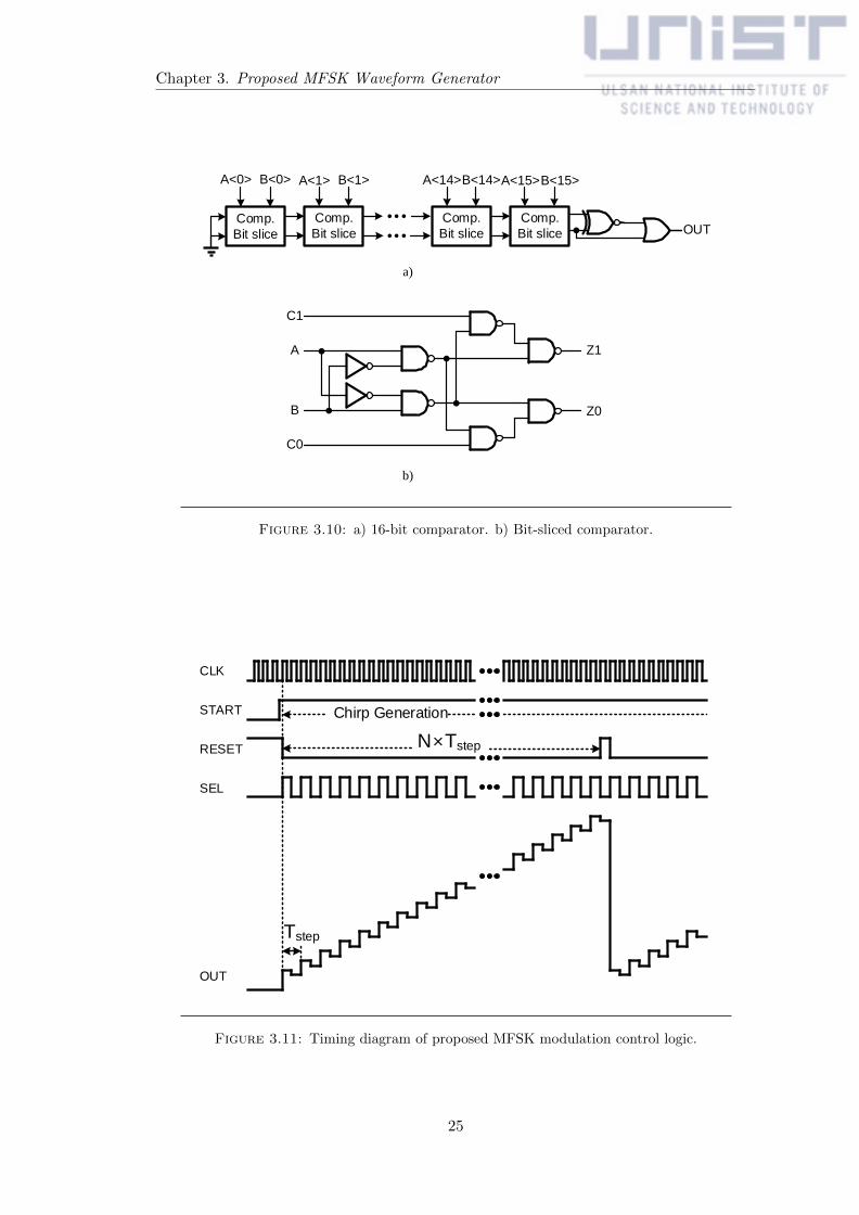
3.2 MFSK Modulation Control Logic
Figure 3.8 illustrates the circuit design of the MMCL. The main components of the
MMCL are an accumulator based on an adder/subtractor, accompanied by an adder
and a comparator. The input codes are selected by a multiplexer. In the MFSK scheme,
the waveform consists of two linear frequency signals, which are transmitted in an inter-
twined way. In order to realize the FSK modulation in each time step, the clock signal
for the MMCL is divided by two. Therefore, the output will be changed every half step
Tstep.
For the adder, the Ripple-Carry Adder (RCA) architecture is employed because of the
low operating frequency and the output contains 16 bits. Each element of 16-bit adder
is a full adder. There is variety of topology to implement the full adder. In this work,
a conventional full adder with 28 transistors is adopted. The circuit design is shown in
Figure 3.9-a. This adder will be re-used in the design of ∆ − Σ modulator. In order
to switch the role of the accumulator between the adder and subtractor functions, an
XOR gate is added to precede each input. The accumulator performs addition whenever
the SEL signal is low, and the subtracting operating is performed if the SEL signal goes
high. The selection of the adder or subtractor function will be simultaneously conducted
with the two inputs INC and STEP. In other words, the control code will be linearly
increased by the INC value, but the output decreases by the amount of STEP in a time
step. Figure 3.9-b depicts the adder/subtractor design.
The bandwidth of the modulation waveform is specified by the MIN and BW values.
The number of steps can be specified using these two parameters. The sum of MIN
and BW is the maximum boundary of the modulation. The maximum value is detected
22

Chapter 3. Proposed MFSK Waveform Generator
16
INC
MIN
CLK
BW
OUT
MU
XMU
X
16
STEP
A
B
A±B
A
B
A+B
Comp
z-1
z-1
MIN
16
16
ResetSEL
START
16
16
16
16
16
Div2
016
MU
XM
UX
MU
XMU
X
MIN
BW
INC
STEP
START
Figure 3.8: Block diagram of proposed MFSK modulation control logic.
using a 16-bit comparator. This comparator is a chain of bit sliced comparators, as
shown in Figure 3.10-a. However, this architecture has two outputs, which are inferior
and superior, thus several logic gates are added to generate the expected output.
The operation of the MMCL is explained as follows. Initially, the START signal is low;
thus, the output of MMCL is fixed at zero. Therefore, the divider contains the lowest
value, or lowest output frequency. At the same time, a RESET signal is generated.
The chirp generation is started when the START goes high, and the modulation begins
with the minimum value MIN. The SEL signal is high, so the accumulator operates as
a subtractor. The content of the accumulator decreases by the amount of STEP, and
FSK modulation is achieved. In the next cycle, the output is increased by a step of INC
because of the low level of SEL. The FSK modulation is conducted, and the process is
repeated until the maximum boundary. At the end of the chirp, the RESET signal is
generated at the last FSK step. The reset circuit will clear the content of the accumu-
lator, set the output to the minimum value again and start a new chirp. It also ensures
that the last FSK modulation will be conducted.
3.3 MFSK Transceiver Implementation
The waveform generator is embedded into the transceiver assembly from the MMICs.
The Frequency Multiplier includes a power amplifier, which exhibits a typical output
23

Chapter 3. Proposed MFSK Waveform Generator
FAFAFAFA
M
A<0> B<0> A<1> B<1> A<14>B<14>A<15>B<15>
S<0> S<1> S<14> S<15>
A
B BA
A
A B
B
A
BBA
A
B
B
A
Cin
Cin
Cin S
Cout
a)
b)
Figure 3.9: a) Full Adder circuit. b) Adder/Subtractor circuit
power of 15 dBm. In the receiver chain, the input signal is firstly amplified by a Low
Noise Amplifier (LNA), which has a signal gain of 15 dB and Noise Figure (NF) of 4.5
dB. Then, the signal is down-converted into the baseband by the I/Q Mixer. The Local
Oscillator (LO) signal for the mixer is taken from the transmitted signal using a power
splitter. Two similar amplification stages, with a gain of 21.2 dB, follow the mixer. The
last stage is a Variable Gain Amplifier (VGA) with Automatic Gain Control (AGC).
This amplifier has a broad-range analog variable gain from -2.5 dB to +42.5 dB. The
design of the transceiver from the MMICs is based on the front-end module in [16].
The hardware realization of the transceiver is depicted in Fig. 3.12. The transceiver
is packaged in the housing with size (HxWxD) of 90mmx65mmx23mm. Note that this
radar sensor is not included the signal processing part and the antennas.
24
Chapter 3. Proposed MFSK Waveform Generator
C1
A
B
C0
Z1
Z0
Comp.
Bit slice
Comp.
Bit slice
Comp.
Bit sliceComp.
Bit slice OUT
A<0> B<0> A<1> B<1> A<14>B<14>A<15>B<15>
a)
b)
Figure 3.10: a) 16-bit comparator. b) Bit-sliced comparator.
OUT
SEL
RESET
START
CLK
Chirp Generation
Tstep
N×Tstep
Figure 3.11: Timing diagram of proposed MFSK modulation control logic.
25

Chapter 3. Proposed MFSK Waveform Generator
a)
b)
Dimensions (HxWxD):
90mmx65mmx23mm
Figure 3.12: Hardware implementation a) RF part. b) Baseband part.
26
Chapter 4
System Performance Results
4.1 MFSK Waveform Generator
In order to analyze the operation of the proposed waveform generator architecture, the
modulated frequency synthesizer is presented at the behavioral simulation level. In
the discussion to follow, the models are system level simulations. The parameters of
the PLL were estimated using the PLL Design Assistant (PDA) tool [24]. Based on
the real hardware implementation, parameters such as the reference, loop bandwidth,
and noise of the PLL were chosen to ensure that the simulation was close to the real
design. The contribution of the detector noise to the phase noise was -85 dBc/Hz, and
the VCO exhibited -115 dBc/Hz at 10 MHz. The simulation was performed using the
CppSim behavioral level based on C++ [25]. This framework uses uniform time step
with conservation area. The performance of this simulator is confirmed in [26]. From
the circuit implementation, the MMCL was modeled using top-level blocks, and then
included in the fractional-N PLL. The output of the generator was modulated using a
time interval of 0.64 ms because of the limitations of the simulation tools (maximum
simulation time is 1 ms). In the coherent processing interval of 0.64 ms, there are 64
time steps. The simulation results demonstrated the operation of the proposed scheme,
as shown in Figure 4.1.
The proposed waveform generator has a programmable modulation capability that
controls the chirp bandwidth, offset frequency, frequency step and frequency shift. In
order to verify its operation, different chirps with different parameters were generated.
As shown in Figure 4.2, the output signal was modulated in a bandwidth of 150 MHz,
which gives a range resolution of 1m. The time step was 20 µs and there were 256 steps
in total. Thus, the chirp time was around 5.12 ms. Similar to [6], the frequency steps
and frequency increase were -294 kHz and 588 kHz, respectively.
27

Chapter 4. System Performance Results
Figure 4.1: Simulation results of proposed architecture.
150 MHz
294 kHz
5.12 ms
Figure 4.2: MFSK waveform: Bsw=150 MHz, TCPI=5.12 ms, N=256, Tstep=20 µs,fstep=-294 kHz, finc=588 kHz.
A large bandwidth leads to a higher velocity resolution, and a shorter modulation time
can reduce the velocity error caused by the variation of the target speed. Thus, Figure 4.3
shows the modulation with a bandwidth of 300 MHz and the coherent processing interval
of 2.56 ms. The frequency step is twice that of previous cases. The FSK modulation
is realized in Tstep of 10 µs. By setting the same parameters as in the first case, but
changing the number of steps to 128, the bandwidth is decreased to 75 MHz. This low
bandwidth leads to the range resolution of 2 m. However, the velocity resolution is
dependent on the chirp time, the short sweep leads to the large speed resolution. Figure
4.4 illustrates the output waveform of this setting. The parameter INC of the MMCL
has the ability to control the frequency increase in the MFSK waveform. This frequency
shift can be programmed to a random value. The frequeny increase is three times the
frequency step, which means finc=882 kHz, as shown in Figure 4.5.
The beat frequency and phase difference depend on the waveform parameters. A larger
frequency step may cause a measurement error because of the limitation of the phase
difference range. Therefore, the waveform parameters need to be carefully chosen. A
28

Chapter 4. System Performance Results
300 MHz
558 kHz
2.56 ms
Figure 4.3: MFSK waveform: Bsw=300 MHz, TCPI=2.56 ms, N=256, Tstep=10 µs,fstep=-588 kHz, finc=1167 kHz.
75 MHz
294 kHz
1.28 ms
Figure 4.4: MFSK waveform: Bsw=150 MHz, TCPI=1.28 ms, N=128, Tstep=10 µs,fstep=-294 kHz, finc=588 kHz.
longer coherent processing time would affect the relative velocity measurement because
of the fast change in speed.
4.2 Improvement of Target Detection
In order to compare the detection abilities of the FMCW and MFSK waveforms, two
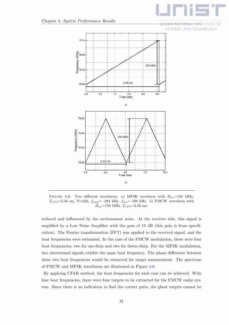
waveforms with the same bandwidth and same chirp time were generated. The FMCW
waveform could be achieved by modifying the input parameters of the dual FMCW
waveform generator [27]. Figure 4.6 shows the measured results for the FMCW and
MFSK waveforms. The bandwidth and chirp time of the two waveforms were set to 150
MHz and 2.56 ms [6], respectively. The MFSK modulation waveform was the optimum
for achieving the highest detection ability. In other words, the frequency step was half of
the frequency increase. These waveform generators are components of the transceivers,
29

Chapter 4. System Performance Results
882 kHz225 MHz
294 kHz
2.56 ms
Figure 4.5: MFSK waveform: Bsw=225 MHz, TCPI=2.56 ms, N=256, Tstep=10 µs,fstep=-294 kHz, finc=882 kHz.
which have the same specifications. Because of the lack of antennas, a top-level simula-
tion was conducted, in which the transceiver was modeled using its parameters, including
the transmitted power, gain of the transmitter/receiver, and the Noise Figure (NF) of
the receiver. It was assumed that the TX and RX antennas had the same gain of 20 dB
[10].
The transceivers with two modulation waveform generators were configured in Matlab.
The performance of the front-end is summarized in Table 4.1. In these simulations, there
were two targets with different distances and velocities. Assuming that the radar was
on the car with a speed of 60 km/h. The two targets are a car and a truck. The car was
at 50 m from the radar with a speed of 50 km/h. The radar and the car had the same
direction. The second target is a truck at 30 m, with an absolute velocity of 55 km/h
towards the radar. Note that the Radar Cross Section (RCS) was associated with the
velocity of the targets [28]. In the signal processing part, a Constant False Alarm Rate
(CFAR) detection method is adopted. The false alarm probability is set to 10−2.
The spectrogram of the FMCW and MFSK waveforms is depicted in Figure 4.7. Both
Table 4.1: Modeling parameters of the front-end module
PA output power Pt [dBm] 15Transmitter gain At [dB] 11TX antenna gain Gt [dBi] 20RX antenna gain Gr [dBi] 20Wave length λ [mm] 3.9Receiver NF NR [dB] 4.5Receiver gain Ar [dB] 15
signals were modulated in the bandwidth of 150 MHz within the chirp interval of 2.56
ms.
The transmitted signal is reflected from the targets. The received signal is significantly
30
Chapter 4. System Performance Results
150 MHz
2.56 ms
150 MHz
5.12 ms
a)
b)
Figure 4.6: Two different waveforms: a) MFSK waveform with Bsw=150 MHz,TCPI=2.56 ms, N=256, fstep= -294 kHz, finc= 588 kHz. b) FMCW waveform with
Bsw=150 MHz, TCPI=2.56 ms.
reduced and influenced by the environment noise. At the receiver side, this signal is
amplified by a Low Noise Amplifier with the gain of 15 dB (this gain is from specifi-
cation). The Fourier transformation (FFT) was applied to the received signal, and the
beat frequencies were estimated. In the case of the FMCW modulation, there were four
beat frequencies, two for up-chirp and two for down-chirp. For the MFSK modulation,
two intertwined signals exhibit the same beat frequency. The phase difference between
these two beat frequencies would be extracted for target measurement. The spectrum
of FMCW and MFSK waveforms are illustrated in Figure 4.8.
By applying CFAR method, the beat frequencies for each case can be achieved. With
four beat frequencies, there were four targets to be extracted for the FMCW radar sys-
tem. Since there is no indication to find the correct pairs, the ghost targets cannot be
31

Chapter 4. System Performance Results
a)
b)
Figure 4.7: a) Spectrogram of FMCW waveform. b) Spectrogram of MFSK waveform.
avoided. In contrast to FMCW radars, the MFSK system uses the beat frequency and
the phase difference. Therefore, only two targets was estimated without any ghost tar-
gets. The targets of these two systems are listed in Table 4.2. The results demonstrated
an improvement in the target detection ability in multi-target situations.
Table 4.2: Estimated targets of FMCW and MFSK radars
Modulation FMCW
Number of targets 4
Range (m) 30.0000 50.0000 21.0000 59.0000
Radial velocity (m/s) 31.9602 3.0438 25.1116 9.8925
Modulation MFSK
Number of targets 2
Range (m) 30.8870 50.6958
Radial velocity (m/s) 31.8742 2.8123
4.3 Discussion
The simulation and measured results of the proposed radar sensor were presented in the
above section. These results demonstrate the operation of the proposed MFSK waveform
32

Chapter 4. System Performance Results
a)
b)
Figure 4.8: a) Spectrum of FMCW waveform. b) Spectrum of MFSK waveform.
generator and the improvement in the target detection in multi-target situations. The
target ranges estimated from the MFSK showed worse values than in the case of the
FMCW waveform. However, the radial velocities exhibited better values because the
MFSK waveform has a shorter chirp time. This modulation waveform absolutely avoids
the effect of ghost targets with a short chirp time. The proposed architecture revealed
significant improvement in the detection ability in multi-target scenarios.
33

Chapter 4. System Performance Results
In this thesis, the designs of waveform generator and transceiver are considered and
implemented. Nevertheless, due to the limitation , the proposed architecture was not
fully integrated. The fractional-N PLL operates at 12.65-12.85 GHz to ease the circuit
design. Thus, a frequency multiplier is needed. This work is the initial results of the
77 GHz MFSK automotive radar, it will be developed and finished in the near future.
A fully integrated CMOS transceiver has been designing for high integration, low cost,
low power.
34

Chapter 5
Future Work and Research
Nowadays, the automotive radar applications are still an active area, especially when the
ability of designing microwave circuits using CMOS process for low cost, high integration.
The modulation waveform generator for automotive radar applications is a promising
area. In this Chapter, the new applications of using our proposed waveform generator
are presented, the development of circuit design and different modulation signals to
improve detection ability is discussed.
The choice of 77 GHz band offers advantages over the old 24 GHz band. The size of
the radar sensor can be very compact with high integrated chip. In this research, the
transceiver was implemented by combining the integrated circuit and MMICs. Thus,
it suffers from large size, high power consumption, and high cost. In addition, the
VCO generates 12.65-12.85 GHz signal instead of 77 GHz, and the structure requires
the frequency doublers and triplers. The 77 GHz FMCW transceivers have recently
presented using 65 nm CMOS technology. By designing the VCO operating at 77 GHz,
the system can eliminate the use of mm-wave blocks, simplify the circuit design. For
further cost reduction and high integration, whole MFSK transceiver would be designed
using CMOS process, which can achieve an advantage of low power consumption.
The MFSK waveform was developed to fulfils the requirement of automotive radar, even
in multi-target scenarios. The target estimation is based on phase measurement, which
suffers from low accuracy due the the low signal-to-noise (SNR). The chirp sequence is
proposed to improve the target measurement and the accuracy of the estimation. This
enhancement in measurement is based on two independent frequency measurements
without using the phase difference. The transmitted signal is a sequence of triangular
chirps which are shrunk to very short time. The principle waveform and the detection
process is illustrated in Figure 5.1. The target range and radial velocity are dependent
on the beat frequency like FMCW waveform. After FFT transformation, targets with
different distances are determined. Then, the second FFT is applied for estimating the
35

Chapter 5. Future Work and Research
Tchirp
Bsw
TCPIt
fT(t)
fB
Down-convert
f(t)
t
FF
T
fB
vr,RFF
T
FF
T
FF
T
FF
T
FF
T
FF
T
FF
T
FF
T
FF
TFFTFFTFFTFFTFFTFFTFFTFFTFFTFFT
fB R
vr
Transmitted signal
Received signal
Figure 5.1: Principle and signal processing of chirp sequence.
Doppler frequency, or radial velocity. The target parameters, range and radial velocity,
are calculated from the measured results from the Doppler and beat frequency.
fD = − 2
λvr (5.1a)
fB = − 2
λvr −
BswTCPI
2
cR (5.1b)
The applications of short-range radars in monitoring vital signs without contact has
recently paid attention of researchers. Radars become an promising approach to remote
real-time health care - mainly monitoring heartbeats and respiration. Currently, in the
healthcare context, contact sensors - transducers, are adopted. However, people feel not
comfortable wearing contact sensors all the time, especially for long-term monitoring
such as monitoring of sudden infant death syndrome, sleep apnea, etc. With the use of
CW radar, the signal can be transmitted with higher energy, thus the SNR is improved.
In other words, high accuracy measurements can be achieved. Differ from the Doppler
radar, the CW radars can extract absolute range of the target. The FMCW is applied
36

Chapter 5. Future Work and Research
MFSK
waveform
generator
Amplifier
ADC Amplifier
Mixer
Heartbeat
Respiration
Position
TX
RX
Figure 5.2: Vital sign detection system using MFSK waveform.
in monitoring the vital signs and attained some initial results. This system has ability
to minimize the effects of surrounding clutter which is the drawback of the Doppler
radar. Nevertheless, the limitation of this waveform in multiple targets can reduce
the performance of the system. The non-contact monitoring radars can accompany the
MFSK modulation, and combine two functions, the positioning and detecting vital signs
as shown in Figure 5.2.
37

Chapter 6
Summary and Conclusion
An introduction of automotive radar applications and the need of the radar sensor to
improve the safety of driving task were presented in Chapter 1. The detection ability of
automotive radar sensors is highly dependent on the modulation waveform, especially in
multi-target situations. In this chapter, three different modulations, FMCW, FSK and
MFSK, were discussed. The MFSK waveform exhibits a promising solution which can
avoid the ghost targets in FMCW and the targets can be solved with high range and high
velocity resolution. From this discussion, several approaches to generate the expected
modulation were discussed in Chapter 2. Three methods, Diophantine PLL, DDFS
and Fractional-N PLL, were introduced. Chapter 3 was presented the proposed system
in which a modulation control logic incorporates a fractional-N PLL for modulating
the output signal. The proposed structure was implemented in a standard 0.13 - µm
CMOS technology and MMICs. The fractional-N PLL is designed to operate at 12.65-
12.85 GHz. Thus, a multiplier by 6 was adopted to ensure the system can generate
the modulation signal in the range of 76-77 GHz. Prior to realizing hardware, the
proposed structure was simulated using CppSim with the help of PLL Design Assistant
in calculating the PLL parameters. The simulation results demonstrated the capability
of generating MFSK modulation. The measured results confirmed the operating of the
proposed structure which is verified in variety settings of inputs as can be seen in Chapter
4. Moreover, the detection ability of MFSK automotive radars was illustrated through
simulations in the comparison to the FMCW radars. Although, most popular radar
sensors in the market are using FMCW, the requirement of more effective modulations
and its hardware implementation are really challenging researchers around the world.
The proposed research provides a better solution for the current sensors and can be a
promising system in the near future.
38

Bibliography
[1] Fulvio Gini, Antonio De Maio, and Lee Patton. Waveform Design and Diversity for
Advanced Radar Systems. The Institution of Engineering and Technology, London,
2012. ISBN 978-1-84919-266-8.
[2] Merrill Ivan Skolnik. Introduction to Radar Systems. McGraw-Hill, New York, third
edit edition, 2002.
[3] Jri Lee, Yi An Li, Meng Hsiung Hung, and Shih Jou Huang. A fully-integrated
77-GHz FMCW radar transceiver in 65-nm CMOS technology. IEEE Journal of
Solid-State Circuits, 45(12):2746–2756, 2010. ISSN 00189200. doi: 10.1109/JSSC.
2010.2075250.
[4] Tang Nian Luo, Chi Hung Evelyn Wu, and Yi Jan Emery Chen. A 77-GHz CMOS
automotive radar transceiver with anti-interference function. IEEE Transactions on
Circuits and Systems I: Regular Papers, 60(12):3247–3255, 2013. ISSN 15498328.
doi: 10.1109/TCSI.2013.2265974.
[5] A.G. Stove. Linear FMCW radar techniques. In IEE Proceedings F Radar and
Signal Processing, volume 140, page 137, 1993. ISBN 0956-375X. doi: 10.1049/
ip-f-2.1993.0019.
[6] H. Rohling and M.-M. Meinecke. Waveform design principles for automotive radar
systems. In 2001 CIE International Conference on Radar Proceedings, volume 1,
pages 1–4, 2001. ISBN 0-7803-7000-7. doi: 10.1109/ICR.2001.984612.
[7] Hermann Rohling, Steffen Heuel, and Henning Ritter. Pedestrian detection pro-
cedure integrated into an 24 GHz automotive radar. In IEEE National Radar
Conference - Proceedings, pages 1229–1232, 2010. ISBN 9781424458127. doi:
10.1109/RADAR.2010.5494432.
[8] Hermann Rohling. Milestones in radar and the success story of automotive radar
systems. In Radar Symposium (IRS), 2010 11th International, 2010. ISBN 978-1-
4244-5613-0.
39

Bibliography
[9] M Pichler, M Pichler, A Stelzer, A Stelzer, P Gulden, P Gulden, C Seisen-
berger, C Seisenberger, M Vossiek, and M Vossiek. Phase-error-measurement and
-compensation in PLL frequency synthesizers for FMCW sensors-II: Theory. IEEE
Trans. Circuits Syst. I, Reg. Papers, Jun, 54(5):1006–1017, 2007.
[10] Toshiya Mitomo, Naoko Ono, Hiroaki Hoshino, Yoshiaki Yoshihara, Osamu Watan-
abe, and Ichiro Seto. A 77 GHz 90 nm CMOS transceiver for FMCW radar applica-
tions. IEEE Journal of Solid-State Circuits, 45(4):928–937, 2010. ISSN 00189200.
doi: 10.1109/JSSC.2010.2040234.
[11] Paul Peter Sotiriadis. Diophantine frequency synthesis. IEEE Transactions on
Ultrasonics, Ferroelectrics, and Frequency Control, 53(11):1988–1998, 2006. ISSN
08853010. doi: 10.1109/TUFFC.2006.139.
[12] Paul Peter Sotiriadis. Diophantine frequency synthesis for fast-hopping, high-
resolution frequency synthesizers. IEEE Transactions on Circuits and Systems II:
Express Briefs, 55(4):374–378, 2008. ISSN 15497747. doi: 10.1109/TCSII.2008.
919499.
[13] William F. Egan. Advanced Frequency Synthesis by Phase Lock. John Wiley &
Sons, Inc, New Jersey, 2011. ISBN 978-0-470-91566-0.
[14] Yoichi Kawano, Toshihide Suzuki, Masaru Sato, Tatsuya Hirose, and Kazukiyo
Joshin. A 77GHz transceiver in 90nm CMOS. Digest of Technical Papers - IEEE
International Solid-State Circuits Conference, pages 310–312, 2009. ISSN 01936530.
doi: 10.1109/ISSCC.2009.4977432.
[15] Hoon Hee Chung, Umar Lyles, Tino Copani, Bertan Bakkaloglu, and Sayfe Kiaei.
A bandpass ∆Σ DDFS-driven 19GHz frequency synthesizer for FMCW automotive
radar. In Digest of Technical Papers - IEEE International Solid-State Circuits
Conference, pages 126–128, 2007. ISBN 1424408539. doi: 10.1109/ISSCC.2007.
373620.
[16] Winfried Mayer, Martin Meilchen, Wilfried Grabherr, Peter Nuchter, and Rainer
Guhl. Eight-channel 77-GHz front-end module with high-performance synthe-
sized signal generator for FM-CW sensor applications. IEEE Transactions on
Microwave Theory and Techniques, 52(3):993–1000, 2004. ISSN 00189480. doi:
10.1109/TMTT.2004.823548.
[17] Didier Salle, Christophe Landez, Pierre Savary, Gilles Montoriol, and Robert Gach.
A Fully Integrated 77GHz FMCW Radar Transmitter Using a Fractional-N Fre-
quency Synthesizer. In Proceedings of the 6th European Radar Conference, number
October, pages 149–152, 2009. ISBN 9782874870149.
40

Bibliography
[18] Tang Nian Luo, Chi Hung Evelyn Wu, and Yi Jan Emery Chen. A 77-GHz CMOS
FMCW frequency synthesizer with reconfigurable chirps. IEEE Transactions on
Microwave Theory and Techniques, 61(7):2641–2647, 2013. ISSN 00189480. doi:
10.1109/TMTT.2013.2264685.
[19] Joonhong Park, Hyuk Ryu, Keum-Won Ha, Jeong-Geun Kim, and Donghyun Baek.
76 – 81-GHz CMOS Transmitter With a. IEEE Transactions on Microwave Theory
and Techniques, 63(4):1399–1408, 2015. ISSN 00189480. doi: 10.1109/TMTT.2015.
2406071.
[20] Vipul Jain, Babak Javid, and Payam Heydari. A BiCMOS dual-band millimeter-
wave frequency synthesizer for automotive radars. IEEE Journal of Solid-State
Circuits, 44(8):2100–2113, 2009. ISSN 00189200. doi: 10.1109/JSSC.2009.2022299.
[21] H. P. Forstner, H. Knapp, H. Jage, E. Kolmhofer, J. Platz, F. Starzer, M. Treml,
A. Schinko, G. Birschkus, J. Bock, K. Aufinger, R. Lachner, T. Meister, H. Schafer,
D. Lukashevich, S. Boguth, A. Fische, F. Reininge, L. Maure, J. Minichshofe, and
D. Steinbuch. A 77GHz 4-channel automotive radar transceiver in SiGe. In Digest
of Papers - IEEE Radio Frequency Integrated Circuits Symposium, pages 233–236,
2008. ISBN 9781424418091. doi: 10.1109/RFIC.2008.4561425.
[22] Nils Pohl, Timo Jaeschke, and Klaus Aufinger. An ultra-wideband 80 GHz FMCW
radar system using a SiGe bipolar transceiver chip stabilized by a fractional-N PLL
synthesizer. IEEE Transactions on Microwave Theory and Techniques, 60(3 PART
2):757–765, 2012. ISSN 00189480. doi: 10.1109/TMTT.2011.2180398.
[23] Young Shig Choi and Dae Hyun Han. Gain-boosting charge pump for current
matching in phase-locked loop. IEEE Transactions on Circuits and Systems II:
Express Briefs, 53(10):1022–1025, 2006. ISSN 10577130. doi: 10.1109/TCSII.2006.
882122.
[24] C.Y. Lau and M.H. Perrott. Fractional-N frequency synthesizer design at the trans-
fer function level using a direct closed loop realization algorithm. In Proceedings
2003. Design Automation Conference (IEEE Cat. No.03CH37451), pages 526–531,
2003. ISBN 1-58113-688-9. doi: 10.1109/DAC.2003.1219063.
[25] Michael H Perrott. Fast and Accurate Behavioral Simulation of Fractional-N Fre-
quency Synthesizers and other PLL / DLL Circuits. pages 498–503, 2002. ISBN
1581134614.
[26] Michael H Perrott, Mitchell D Trott, and Charles G Sodini. A Modeling Approach
for SD Fractional-N Frequency Synthesizer Allowing Straightforward Noise Analy-
sis. IEEE Journal of Solid State Circuits, 37(8):1028–1038, 2002.
41

Bibliography
[27] Ngoc Quang Nguyen, MyoungYeol Park, YoungSu Kim, and Franklin Bien. A
24-GHz dual FMCW waveform generator to improve target detection of automo-
tive radar applications. In 2015 International Conference on Green and Human
Information Technology, 2015.
[28] a. Bazzi, C. Karnfelt, A. Peden, T. Chonavel, P. Galaup, and F. Bodereau. Esti-
mation techniques and simulation platforms for 77 GHz FMCW ACC radars. The
European Physical Journal Applied Physics, 57:11001, 2012. ISSN 1286-0042. doi:
10.1051/epjap/2011110031.
42