Embed Size (px)
Citation preview

Optical Materials 36 (2014) 936–940
Contents lists available at ScienceDirect
Optical Materials
journal homepage: www.elsevier .com/locate /optmat
A 2D l-Raman analysis of low repetition rate femto-waveguidesin lithium niobate by using a finite element model
0925-3467/$ - see front matter � 2014 Elsevier B.V. All rights reserved.http://dx.doi.org/10.1016/j.optmat.2013.12.040
⇑ Corresponding author. Tel.: +54 2214840280; fax: +54 2214712771.E-mail address: [email protected] (M.R. Tejerina).
M.R. Tejerina a,⇑, D. Jaque b, G.A. Torchia a
a Centro de Investigaciones Ópticas CONICET La Plata CIC, Camino Centenario y 506 s/n M.B. Gonnet (1897), Pcia Buenos Aires, Argentinab Departamento de Física de Materiales, Facultad de Ciencias C4, Universidad Autónoma de Madrid, Campus de Cantoblanco, 28049 Madrid, Spain
a r t i c l e i n f o a b s t r a c t
Article history:Received 2 October 2013Received in revised form 15 November 2013Accepted 26 December 2013Available online 20 January 2014
Keywords:Lithium niobateFemtosecond laser written opticalwaveguidesRaman shift mappingRefractive index fieldResidual strain field
We present a l-Raman two-dimensional analysis of 1 kHz femtosecond laser written waveguides in anx-cut lithium niobate crystal. At first, the fitting between a two-dimensional elastic model and experi-mental micro Raman spectroscopy data (MR) were examined to validate the numerical model. In this, theRaman Potential Deformation Theory (RPDT) was employed to fit the wavenumber shift of the A1(TO)4
phonon. Then, the adequate values for geometrical parameters of the numerical model (horizontal andvertical ellipse radius) were estimated. Finally, using these parameter values, the guided modes werecomputed for different ellipse expansions and compared with experimental guided modes.
� 2014 Elsevier B.V. All rights reserved.
1. Introduction
Since 1996, ultra-fast (pulses of hundreds of femtoseconds) la-ser writing has emerged as an important tool for optical circuit fab-rication. These guiding structures are essential for technologicalapplications in the field of optical communications in terms ofdeveloping integrated components, amplifiers, and lasers, inter alia[1]. The main advantage of this fabrication method is that it can beapplied to an unlimited number of optical materials. The nonlinearabsorption as a consequence of there being many infrared photonsin the focused region and the later micro-explosion and re-solidifi-cation are the key to obtaining a suitable material modification [1].
Due to the high complexity of the nonlinear interaction, thegeneration of waveguides using different processing parameters(velocity, pulse duration and pulse energy) arose as an empiricalway of improving ultra-fast laser writing [1–3]. As a result, a largenumber of successful integrated guiding structures have been re-ported by using low repetition rate laser processing (1 kHz) [4–8].
Knowledge about femto-waveguides (femtosecond laser writ-ten waveguides) origin get mainly increased because of the quali-tatively comparison between experimental guided regions in themand a numerical elastic model [9–12]. This model consists of ananisotropic domain where an ellipse statically expands, and theresidual mechanical deformation generates, via the piezo-optic
effect, the refractive index increment necessary for wave guiding[13].
Subsequently, the wavenumber shifts of Raman A1(TO) phononswithin a linear path across low repetition femto-waveguides wasqualitatively reported and attributed to residual strain by Ródenaset al. [14]. Following the mentioned assumptions and mergingthem with the previously reported numerical model, we had quan-titative analyzed Raman shifts (using the Deformation PotentialTheory) in a previous work [15]. In this, the Raman scanning wastaken in a linear path across the femto-waveguide and allowed,in a first approximation, the computing of the residual strain field,but only in a linear path. A quantitative two-dimensional descrip-tion of the material structure in the femto-waveguide (laser-mate-rial interaction leading region) is very important when designingphotonic circuits formed by this kind of waveguides because thedeformation field is closely tied to the refractive index field bythe piezo-optic relation [15]. In this sense, in order to extend theone-dimensional approach [15], the current work deals with atwo-dimensional Raman and optical analysis of a femto-wave-guide and includes the following targets: (i) validating a numericalmodel which hypothetically explains the two-dimensional Ramanbehavior; (ii) estimating the adequate values for the model geo-metrical parameters (horizontal and vertical ellipse radii); and(iii) using the obtained geometrical parameters values to computethe guided modes for different expansions and compare them withexperimentally measured guided light.

M.R. Tejerina et al. / Optical Materials 36 (2014) 936–940 937
2. Materials and experimental methods
2.1. Sample characteristics, femtosecond laser processing andwaveguide optical coupling
The waveguide analyzed in this work was performed in anNd:Mg:LiNbO3 x-cut sample. The Nd- and Mg-doping ratios were0.3% and 5%, respectively. The structural modification was gener-ated with a 796 nm Ti: Sapphire ultrafast laser. The duration ofthe pulses was 120 fs with a repetition rate of 1 kHz and energyper pulse of 3 lJ. A 10 � (N.A. = 0.3) microscope objective was usedto focalize the laser inside the crystal. The sample was displaced ata rate of 25 lm/s along the y-axis with a 0.2 lm resolution posi-tioning stage. The structure modification performed in the crystalallowed light guidance; an optical image of the modification canbe seen in Fig. 1(b). The wave-guiding zone is marked with the text‘‘WG’’ and the probe laser spot above the direct modified materialis marked with the text ‘‘PL’’ in this figure.
To perform optical coupling to the generated femto-waveguide,the well-known ‘‘end-fire’’ method was implemented using a stan-dard 630 nm solid state laser [14]. So, the spatial distribution of theguided mode intensity at the waveguide output was measured bymeans of a standard Newport beam profile analyzer.
2.2. 2D l-Raman mapping system and experimental procedure
The residual mechanical deformations in the generated wave-guides were studied with back-scattering l-Raman spectroscopymapping with a y(zz)y configuration. For this mapping, a200 mW argon laser centered at 532 nm and a Confocal OlympusBX-41 with an objective of 50 � (NA = 0.25) were used. A set ofnotch filters and a polarizer were used in the experiment [14].The sample was displaced with a 0.1 lm resolution motorized sta-tion such that a 2D mapping of waveguides with z-direction and x-direction steps of 1 lm was generated. The well-known Ramanspectrum for the LiNbO3 y(zz)y configuration was measured andstored in each point of the mapping. The phonon A1(TO)4 was fittedwith a Lorentzian function, and the energy shift in the analyzedzone was obtained as a 3D surface (energy variation of phononvs. z-displacement vs. x-displacement). The scanning area(70 � 60 lm2) corresponds to the image shown in Fig. 1(b).
3. Theory and numerical calculation
3.1. Raman Deformation Potential Theory (RDPT)
The Raman Deformation Potential Theory (RDPT) relates themechanical deformation of crystals to the energy shift of optical
Fig. 1. (a) Finite element model domain; (b) optical microscopic image corre-sponding to the mapped region.
phonons. Taking into account the symmetry of the A1(TO)i pho-nons, this relationship can be described by [15]:
DEA1ðTOÞi ¼ ei � ðexx þ eyyÞ þ fi � ðezzÞ ð1Þ
In Eq. (1), DEA1ðTOÞi is the wavenumber shift of a ‘‘i’’ phonon ofsymmetry A1(Transverse Optical); ei and fi are the A1 phonon defor-mation potential constants; and exx, eyy and ezz are the elements ofdeformation tensor.
In the current model, exx and ezz are ‘‘surfaces’’ (functions of xand z) which depend on the model parameters values and eyy isequal to zero. So, Eq. (1) will turn into Eq. (2).
DEA1ðTOÞi ¼ ei � exxðz; xÞ þ fi � ezzðz; xÞ ð2Þ
In Eq. (2), it can be seen that the resulting strain field should berelated with the Raman shift field by a linear combination.
3.2. Numerical model for strain field computing
The numerical model used in this work consists of a quarter ofan ellipse which statically expands in an elastic domain. A schemeof the model is shown in Fig. 1(a). The input parameters of themodel are four: the initial horizontal radius (a), the initial verticalradius (b), the horizontal expansion parameter (a = Da/a) and thevertical expansion parameter (b = Db/b). In Fig. 1(a), the geometri-cal input parameters are shown (a and b). And the dashed line nearthe ellipse represents the final geometry after the static expansion(so, the ‘‘after expansion’’ radii are: a + Da and b + Db).
This model represents an arbitrary mechanical expansion whichgenerates a strain field in the waveguide region and therefore, ahypothetically Raman shift variation and a refractive index varia-tion (by means of the piezo-optic effect, Eq. (4)). Physically, thisexpansion is the result of many linear and non-linear complex phe-nomena which, in general, have not been quantitatively and inde-pendently determined yet [8]. The ellipse geometry can be related,in some way, with the focal intensity distribution and the expan-sion represents the focal volume variation occurring after the la-ser-material interaction.
To compute the strain field (exx and ezz) after the ellipse expan-sion, we used a code generated in MATLAB environment. This opencode was published in a previous work [13] and the assumptions/approximations made in this finite element model were detailedin another work, where a linear path of Raman shift across femto-waveguides is analyzed [15]. As mentioned in the cited works, thenumerical model makes the following general assumptions: elasticmaterial, static expansion, plane strain deformations (eyy = 0) andorthotropic approximation for LiNbO3 compliance matrix.
3.3. Method
3.3.1. Setting expansion parameters (a and b) for optimal geometricalparameters computing
In order to make a first evaluation of the model and computethe optimal geometrical parameters (a and b), we set the expan-sion parameters as follows, a = b = 0.01. Taking into account thefollowing:
� a = b; this simplification was introduced by other authors andgave, qualitatively, a good approximation of the guided zonesin femto-waveguides in LiNbO3 [9].� a = b = 0.01; the scope of this work includes the estimation of
the optimal values of a and b ellipse radii for the l-Ramanmap fitting. The absolute value of the expansion does not, how-ever, change the fitting error: this conclusion can be reached byanalyzing Eq. (2); if the numerical expansion is increased, i.e. aand b are increased and if the relation between them is fixed,

Fig. 2. Raman shift mapping of femtosecond waveguide.
Fig. 3. A1TO4 relative Raman shift mapping of averaged quadrants.
938 M.R. Tejerina et al. / Optical Materials 36 (2014) 936–940
the strain fields (ex and ez) obtained after increasing a and b areproportional to those obtained before the increment. So, e and f,which are the fitting parameters, decrease to fit the experimen-tal Raman field and the resultant Raman field and the fit errorwill not change. So, a value of 0.01 for a and b is set becausesimilar values were also found in other papers [9,10].
3.3.2. ProcedureFirstly, the expansion in the numerical model (a and b) was
fixed using values from literature (as explained in Section 3.3.1).Following, the corresponding strain fields (exx and ezz) were com-puted for different values of a (from 0.1 to 3.2 lm) and b (from 6to 12 lm). Then, each pair of the obtained exx and ezz surfaces werefitted (using non-linear square error fitting of MATLAB package:‘‘fminsearch.m’’) to the measured Raman shift mapping by meansof Eq. (2) and using e and f as fitting parameters. Following, the To-tal Square Error (TSE) of each fitting (Eq. (3)) was computed andplotted for each pair of geometrical parameters (a,b) (Fig. 4). Sub-sequently, the different TSE were compared and the optimal valuesof a and b (ao and bo) were obtained.
TSE ¼Xn
i¼1
ðDATOexpðzi; xiÞ � DATOnumðzi; xiÞÞ2 ð3Þ
In Eq. (3), DA1TOexp(zi,xi) is the experimental Raman shift at thecoordinate (zi,xi), DA1TOnum(zi,xi) is the numerically computed Ra-man shift at the coordinate (zi,xi).
Using the obtained optimal geometrical parameters (ao and bo),the guided modes were computed for different expansions values(a and b). To this end, the steps indicated by Okamoto [16] werefollowed. Then, the computed guided modes were compared withexperimentally measured guided light.
In the zone close to the perimeter of the ellipse, plastic effectscan take place because of shock waves after femtosecond interac-tion [3,17,18]. As a result, the elastic numerical approach is notsuitable to fit this zone. Consequently, we removed from the Ra-man mapping domain the area enclosed by a quarter of ellipse ofradii 1.4�a and 1.4�b to adjust the experimental results.
4. Results and discussion
4.1. The 2D l-Raman mapping
As mentioned in Section 2.2, a map of the energy shift of theA1(TO)4 Raman phonon was obtained in low repetition rate(1 KHz) femtosecond waveguides written in a Nd:Mg:LiNbO3 crys-tal. This field is shown in Fig. 2.
In Fig. 2, six principal lobes can be observed: although the pat-tern of the Raman mapping has certain symmetry, so-called ‘‘planesymmetry,’’ (i.e. the curves which are the limits of the six lobesseem to be quasi-symmetric), it can be seen that the ‘‘intensity’’of the different lobes is not symmetric. This asymmetry of the Ra-man shift could be generated by an asymmetric expansion during/after material-femtosecond laser interaction. Although this non-symmetry is reported by other authors [14], its origin and its maincharacteristics are not yet well understood.
The fact that the limits of the lobes are symmetric is in agree-ment with the numerical model proposed, but this does not applyto the lobes ‘‘intensity’’ as they are not fully symmetric. In any case,to test the numerical model and compute the optimal geometricalparameters (a and b), the four quadrants (c1, c2, c3, c4) were aver-aged. As a result, in Fig. 3 we present the averaged spectral shift ina quarter of the domain. Also, in Fig. 3, two main lobes can be de-fined: one of them through the horizontal kl path and anotherthrough the ij path. The ij lobe has a positive Raman shifts whereasthe kl lobes show a negative shift.
4.2. Total Summation Error (TSE) of the l-Raman fitting for differentellipse input parameters (a and b)
The wavenumber shift of phonon A1(TO)4 shown in Fig. 3 wasfitted for different values of the quarter-ellipse radii, and, the TSEwas determined. The result is plotted in Fig. 4.
In Fig. 4, the contour level lines show that, the optimal horizon-tal radius (ao) and the optimal vertical radius (bo) are around1.7 lm and 8.5 lm, respectively.
In Fig. 4, it can also be seen that the value of TSE increases moreslowly for values of b which are above bo, than for those lower thanbo. This suggests that there is a lower limit for the b value, and it isequal to 8 lm.
Analyzing in the same way the behavior of TSE for the values ofa, we clearly see an optimum value of ao around 1.7 and an upperlimit of a of 2 lm can be estimated because for values lower than1.7 lm the TSE surface has a lower slope (see Fig. 4).
In sum, the computed values for ao and bo are 1.7 and 8.5 lmrespectively, but considering the resulting TSE surface it can be sta-ted with more certainty that the upper limit of a and the lower lim-it of b(bl) are 2 lm and 8 lm respectively.
In [15], a linear Raman mapping was used to analyze a similarwaveguide and the values obtained for ao and bo were 0.6 and7.8 respectively. Therefore, a relatively small change (about 10%)was observed in the computed bo parameter and a more importantchange was observed in the computed ao parameter (about 60%),compared with the values computed in the current work. We thinkthat the current result is more representative, because it

Fig. 5. Numerically computed l-Raman shift.
Fig. 6. Computed Dnx field using estimated geometrical parameters (a = 1.7,b = 8.5) and a = 0.01 and b = 0.01.
M.R. Tejerina et al. / Optical Materials 36 (2014) 936–940 939
corresponds to a bidimensional Raman characterization of thewaveguide.
4.3. Fitted l-Raman shift field for optimal geometrical parameters
For the optimal geometrical parameters (a = 1.7 lm andb = 8.5 lm) mentioned in Section 4.2, the resultant numerical l-Raman field is shown in Fig. 5. This figure shows two lobes thatare well defined as observed in the averaged experimental mapshown in Fig. 2: a positive lobe centered along ij path and a nega-tive lobe along kl path (see Fig. 5).
Comparing Fig. 3 with Fig. 5, it can be seen that the numericalresult follows almost the same behavior as that presented in theexperimental Raman mapping. The sum of the square error be-tween them is about 1.2 and the correlation coefficient betweenthem is about 0.9. This indicates that a good fitting is reached usingthe numerical model. Thus, the numerical model should be ade-quate to evaluate the strain field in a two-dimensional femto-waveguide zone.
4.4. Refractive index field for the obtained parameters
In this kind of waveguide, the refractive index variation whichgenerates waveguiding is Dnx [12], which corresponds to the or-dinary refractive index component. For the used values of a andb (0.01) and using the resulting strain field and the piezo-opticexpression shown in Eq. (4) [13], we computed the Dnx residualrefractive index field and it is presented in Fig. 6. It can be seen thatthe refractive index variation has a positive sign along the ij and klpaths, whereas the Raman shift (Fig. 5) has a positive lobe alongthe ij path and a negative lobe along the kl path. This suggests thatthe common simplification used in other works, i.e. that a positive/negative Raman shift necessarily corresponds to a positive/nega-tive refractive index variation, is not always valid. Therefore,strictly speaking, the Raman shift field depends on: residual strainfield; deformation potential constants; and the piezo-optical con-stants of the material. Also, in Fig. 6, in the regions where Dnx (z,x) presents an increment (along path ij and kl), it is possible to con-fine x-polarized light (component in ordinary axis of the electricfield). On the other hand, a large decrease in the refractive indexis observed above the ellipse, so the light polarized in x-axis cannotbe guided in this region [9,19].
Fig. 4. Total Summation Error (TSE) as a function of different geometricalparameters (a and b).
Dnx ¼ 0:5 � n3x � ðp11 � exxðz; xÞ þ p13 � ezzðz; xÞÞ ð4Þ
In Eq. (4), pij are the ij strain piezo-optic elements of lithiumniobate (p11 = �0.026, p13 = 0.174 and nx = 2.28 were used [20])and eij are the ij elements of deformation tensor field.
4.5. Guided modes for different expansions
To evaluate the computed geometrical parameters (ao and bo),after computing respective refractive index field (Dnx), guidedmodes were estimated following the steps indicated by Okamoto[16] for different expansion parameters (a and b). They are pre-sented in Fig. 7(a). In this, the change experimented by the guidedlight when varying the expansion parameters can be observed. InFig. 7(b), experimentally measured guided mode is shown. It canbe seen that the expansion which best fit the experimental guidedmode is that corresponding to a = 0.01 and b = 0. This is enclosedby a red rectangle in Fig. 7(a) and rescaled in Fig. 7(c) for a bettercomparison with experimentally measured guided mode. This re-sult reaffirms the validity of the model and the computed geomet-rical parameters.
5. Conclusions and future works
A two-dimensional Raman map of low repetition rate femto-waveguides in lithium niobate was presented and analyzed using
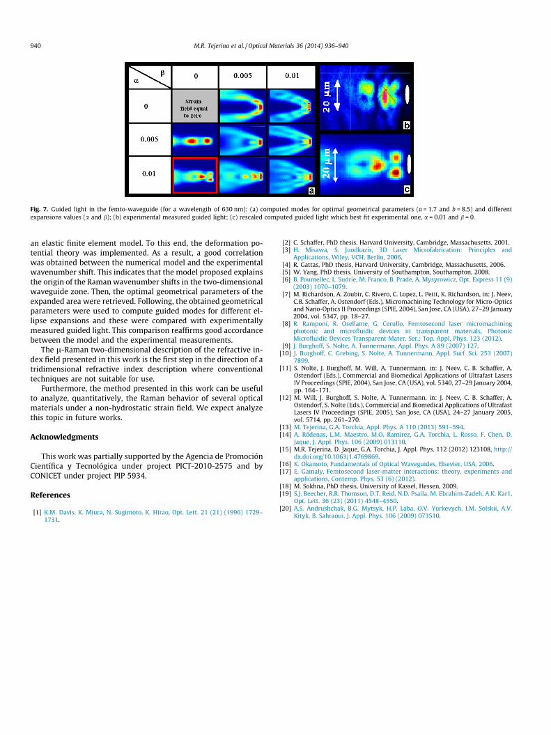
Fig. 7. Guided light in the femto-waveguide (for a wavelength of 630 nm): (a) computed modes for optimal geometrical parameters (a = 1.7 and b = 8.5) and differentexpansions values (a and b); (b) experimental measured guided light; (c) rescaled computed guided light which best fit experimental one, a = 0.01 and b = 0.
940 M.R. Tejerina et al. / Optical Materials 36 (2014) 936–940
an elastic finite element model. To this end, the deformation po-tential theory was implemented. As a result, a good correlationwas obtained between the numerical model and the experimentalwavenumber shift. This indicates that the model proposed explainsthe origin of the Raman wavenumber shifts in the two-dimensionalwaveguide zone. Then, the optimal geometrical parameters of theexpanded area were retrieved. Following, the obtained geometricalparameters were used to compute guided modes for different el-lipse expansions and these were compared with experimentallymeasured guided light. This comparison reaffirms good accordancebetween the model and the experimental measurements.
The l-Raman two-dimensional description of the refractive in-dex field presented in this work is the first step in the direction of atridimensional refractive index description where conventionaltechniques are not suitable for use.
Furthermore, the method presented in this work can be usefulto analyze, quantitatively, the Raman behavior of several opticalmaterials under a non-hydrostatic strain field. We expect analyzethis topic in future works.
Acknowledgments
This work was partially supported by the Agencia de PromociónCientífica y Tecnológica under project PICT-2010-2575 and byCONICET under project PIP 5934.
References
[1] K.M. Davis, K. Miura, N. Sugimoto, K. Hirao, Opt. Lett. 21 (21) (1996) 1729–1731.
[2] C. Schaffer, PhD thesis. Harvard University, Cambridge, Massachusetts, 2001.[3] H. Misawa, S. Juodkazis, 3D Laser Microfabrication: Principles and
Applications, Wiley, VCH, Berlin, 2006.[4] R. Gattas, PhD thesis, Harvard University, Cambridge, Massachusetts, 2006.[5] W. Yang, PhD thesis. University of Southampton, Southampton, 2008.[6] B. Poumellec, L. Sudrie, M. Franco, B. Prade, A. Mysyrowicz, Opt. Express 11 (9)
(2003) 1070–1079.[7] M. Richardson, A. Zoubir, C. Rivero, C. Lopez, L. Petit, K. Richardson, in: J. Neev,
C.B. Schaffer, A. Ostendorf (Eds.), Micromachining Technology for Micro-Opticsand Nano-Optics II Proceedings (SPIE, 2004), San Jose, CA (USA), 27–29 January2004, vol. 5347, pp. 18–27.
[8] R. Ramponi, R. Osellame, G. Cerullo, Femtosecond laser micromachiningphotonic and microfluidic devices in transparent materials, PhotonicMicrofluidic Devices Transparent Mater. Ser.: Top. Appl. Phys. 123 (2012).
[9] J. Burghoff, S. Nolte, A. Tunnermann, Appl. Phys. A 89 (2007) 127.[10] J. Burghoff, C. Grebing, S. Nolte, A. Tunnermann, Appl. Surf. Sci. 253 (2007)
7899.[11] S. Nolte, J. Burghoff, M. Will, A. Tunnermann, in: J. Neev, C. B. Schaffer, A.
Ostendorf (Eds.), Commercial and Biomedical Applications of Ultrafast LasersIV Proceedings (SPIE, 2004), San Jose, CA (USA), vol. 5340, 27–29 January 2004,pp. 164–171.
[12] M. Will, J. Burghoff, S. Nolte, A. Tunnermann, in: J. Neev, C. B. Schaffer, A.Ostendorf, S. Nolte (Eds.), Commercial and Biomedical Applications of UltrafastLasers IV Proceedings (SPIE, 2005), San Jose, CA (USA), 24–27 January 2005,vol. 5714, pp. 261–270.
[13] M. Tejerina, G.A. Torchia, Appl. Phys. A 110 (2013) 591–594.[14] A. Ródenas, L.M. Maestro, M.O. Ramirez, G.A. Torchia, L. Rosso, F. Chen, D.
Jaque, J. Appl. Phys. 106 (2009) 013110.[15] M.R. Tejerina, D. Jaque, G.A. Torchia, J. Appl. Phys. 112 (2012) 123108, http://
dx.doi.org/10.1063/1.4769869.[16] K. Okamoto, Fundamentals of Optical Waveguides, Elsevier, USA, 2006.[17] E. Gamaly, Femtosecond laser-matter interactions: theory, experiments and
applications, Contemp. Phys. 53 (6) (2012).[18] M. Sokhna, PhD thesis, University of Kassel, Hessen, 2009.[19] S.J. Beecher, R.R. Thomson, D.T. Reid, N.D. Psaila, M. Ebrahim-Zadeh, A.K. Kar1,
Opt. Lett. 36 (23) (2011) 4548–4550.[20] A.S. Andrushchak, B.G. Mytsyk, H.P. Laba, O.V. Yurkevych, I.M. Solskii, A.V.
Kityk, B. Sahraoui, J. Appl. Phys. 106 (2009) 073510.