Embed Size (px)
Citation preview
1
A 3.9 ns 8.9 mW 4×4 Silicon Photonic Switch Hybrid-Integrated
with CMOS Driver
A. Rylyakov, C. Schow, B. Lee, W. Green, J. Van Campenhout, M. Yang, F. Doany, S. Assefa, C. Jahnes, J. Kash, Y. Vlasov
IBM T.J. Watson Research Center, Yorktown Heights, NY
2
Outline
• Motivation• Silicon photonics technology overview• Integration strategies: full monolithic and hybrid• 4×4 switch hybrid-integrated with CMOS driver• Conclusion
3
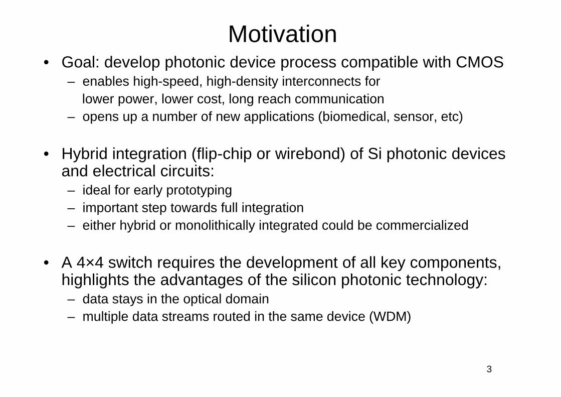
Motivation• Goal: develop photonic device process compatible with CMOS
– enables high-speed, high-density interconnects forlower power, lower cost, long reach communication
– opens up a number of new applications (biomedical, sensor, etc)
• Hybrid integration (flip-chip or wirebond) of Si photonic devices and electrical circuits:– ideal for early prototyping– important step towards full integration– either hybrid or monolithically integrated could be commercialized
• A 4×4 switch requires the development of all key components, highlights the advantages of the silicon photonic technology:– data stays in the optical domain – multiple data streams routed in the same device (WDM)
4
Outline
• Motivation• Silicon photonics technology overview:
– Waveguides (“SOI photonic wires”), other passive devices– Modulators, detectors– Fiber coupling
• Integration strategies: full monolithic and hybrid• 4×4 switch hybrid-integrated with CMOS driver• Conclusion
http://www.research.ibm.com/photonics
5
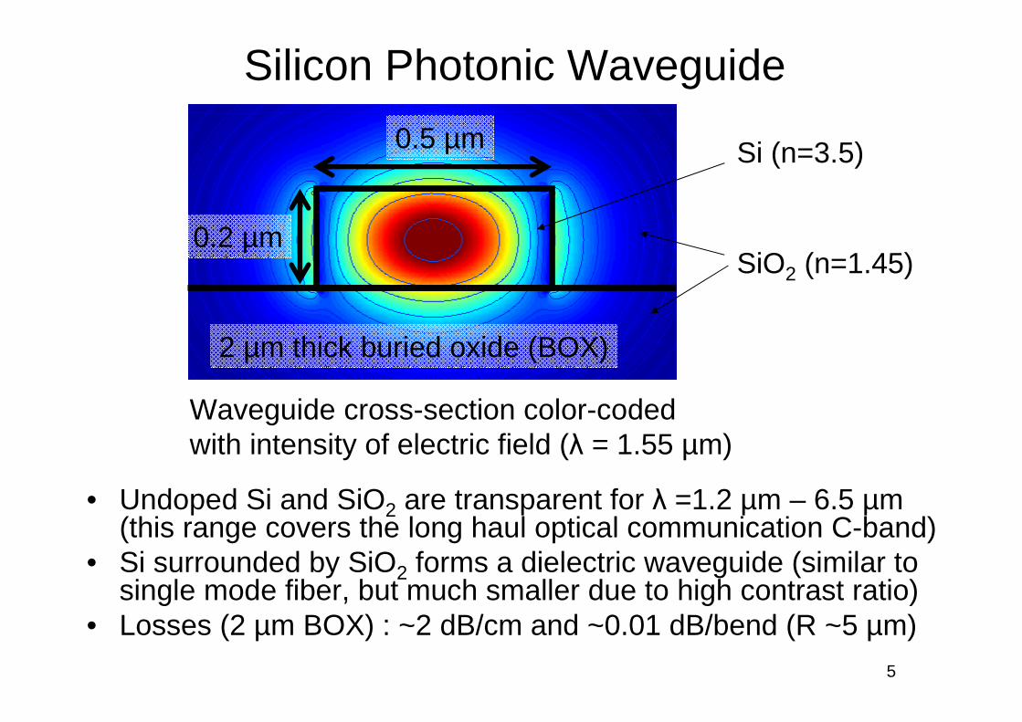
Silicon Photonic Waveguide
0.5 µm
0.2 µm
Si (n=3.5)
SiO2 (n=1.45)
• Undoped Si and SiO2 are transparent for λ =1.2 µm – 6.5 µm (this range covers the long haul optical communication C-band)
• Si surrounded by SiO2 forms a dielectric waveguide (similar to single mode fiber, but much smaller due to high contrast ratio)
• Losses (2 µm BOX) : ~2 dB/cm and ~0.01 dB/bend (R ~5 µm)
2 µm thick buried oxide (BOX)
Waveguide cross-section color-coded with intensity of electric field (λ = 1.55 µm)
6
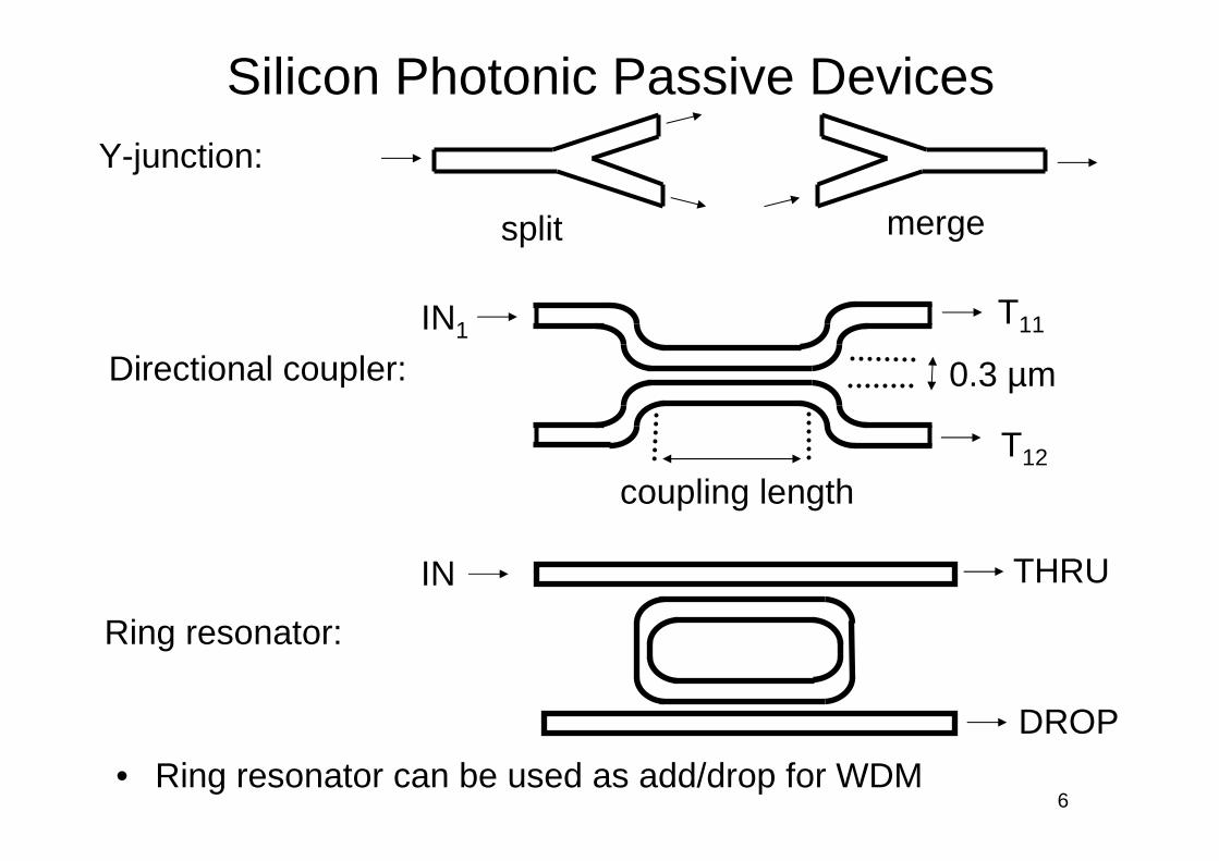
Silicon Photonic Passive Devices
Directional coupler:
Y-junction:
IN1T11
T12
split merge
coupling length
0.3 µm
Ring resonator:
IN THRU
DROP
• Ring resonator can be used as add/drop for WDM
7
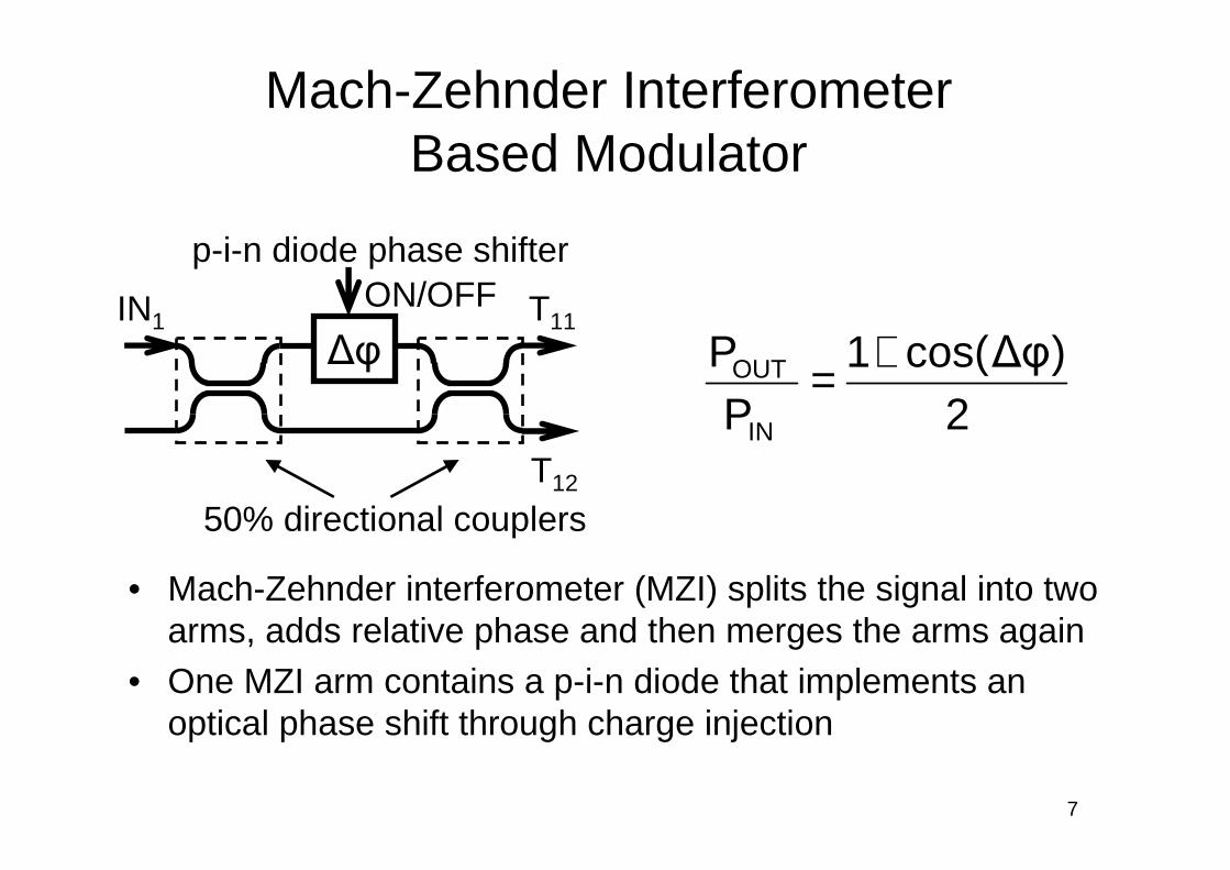
Mach-Zehnder Interferometer Based Modulator
• Mach-Zehnder interferometer (MZI) splits the signal into two arms, adds relative phase and then merges the arms again
• One MZI arm contains a p-i-n diode that implements an optical phase shift through charge injection
IN1
∆φ
p-i-n diode phase shifter
50% directional couplers
T11
T12
ON/OFF
2)∆φcos(1+=
IN
OUT
PP
8
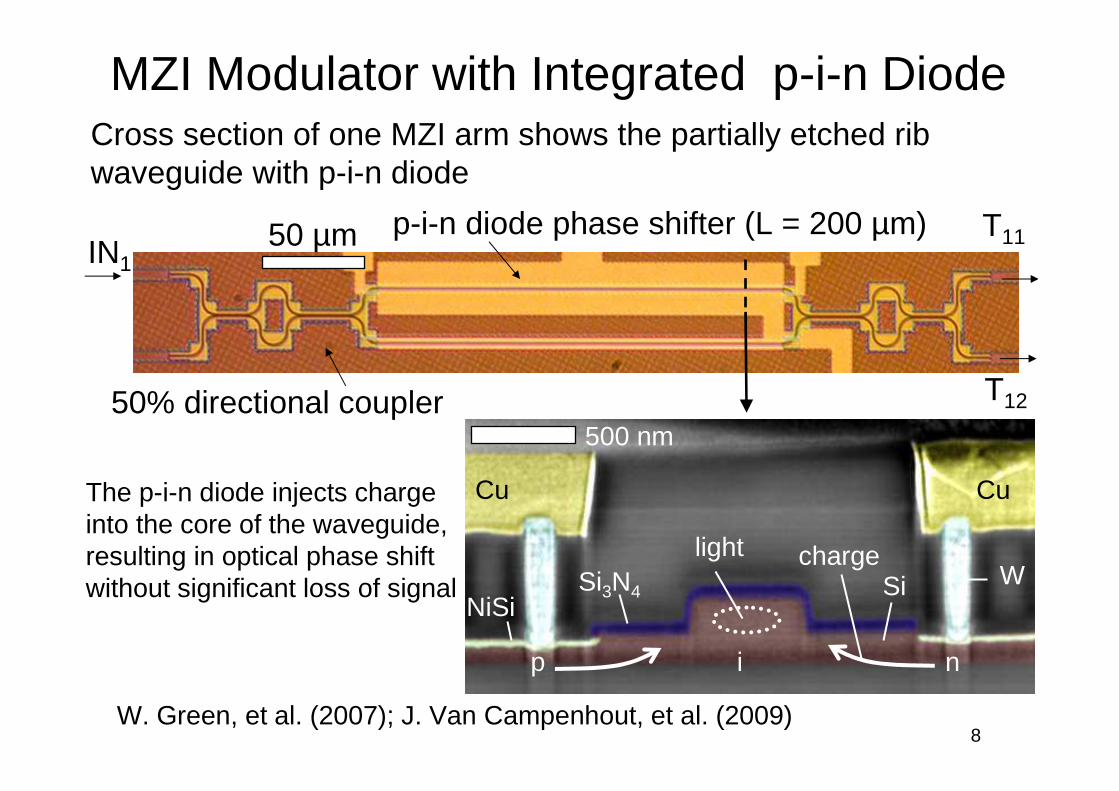
MZI Modulator with Integrated p-i-n Diode
i
NiSiSiSi3N4
W
Cu Cu
p n
500 nm
W. Green, et al. (2007); J. Van Campenhout, et al. (2009)
50 µm p-i-n diode phase shifter (L = 200 µm)
50% directional coupler
IN1
T11
T12
Cross section of one MZI arm shows the partially etched rib waveguide with p-i-n diode
light charge
The p-i-n diode injects chargeinto the core of the waveguide,resulting in optical phase shiftwithout significant loss of signal
9
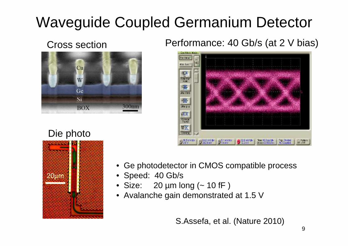
Cross section
Die photo
Performance: 40 Gb/s (at 2 V bias)
• Ge photodetector in CMOS compatible process• Speed: 40 Gb/s• Size: 20 µm long (~ 10 fF )• Avalanche gain demonstrated at 1.5 V
S.Assefa, et al. (Nature 2010)
Waveguide Coupled Germanium Detector
10
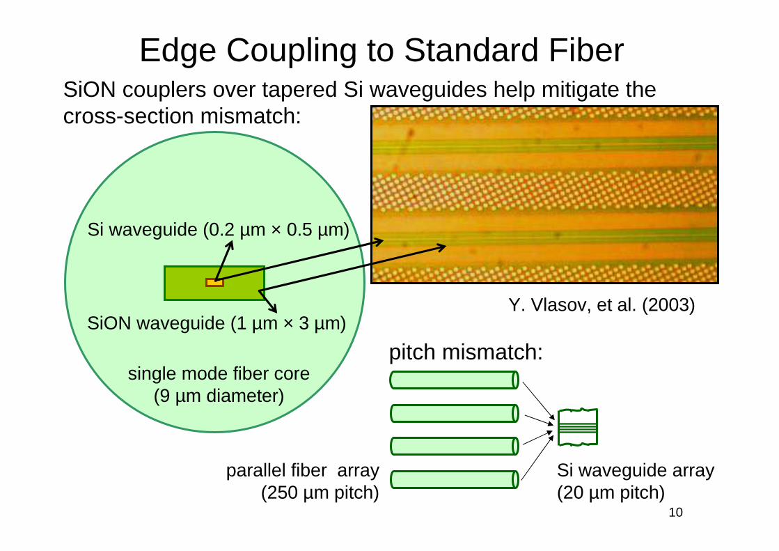
Edge Coupling to Standard FiberSiON couplers over tapered Si waveguides help mitigate the cross-section mismatch:
pitch mismatch:
Si waveguide array(20 µm pitch)
SiON waveguide (1 µm × 3 µm)
single mode fiber core(9 µm diameter)
Si waveguide (0.2 µm × 0.5 µm)
Y. Vlasov, et al. (2003)
parallel fiber array(250 µm pitch)
11
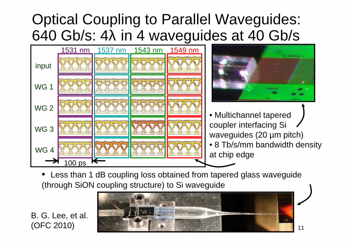
Optical Coupling to Parallel Waveguides:640 Gb/s: 4λ in 4 waveguides at 40 Gb/s
100 ps
input
1531 nm 1537 nm 1543 nm 1549 nm
WG 1
WG 2
WG 3
WG 4
• Multichannel tapered coupler interfacing Si waveguides (20 µm pitch)• 8 Tb/s/mm bandwidth density at chip edge
B. G. Lee, et al.(OFC 2010)
• Less than 1 dB coupling loss obtained from tapered glass waveguide (through SiON coupling structure) to Si waveguide
12
Outline
• Motivation• Silicon photonics technology overview• Integration strategies: full monolithic and hybrid
– Monolithic integration technology announced (SEMICON 2010)– 15 Gb/s detector hybrid-integrated with CMOS receiver (CLEO 2011)– 8 Gb/s ring modulator hybrid-integrated with CMOS driver (OFC 2011)
• 4×4 switch hybrid-integrated with CMOS driver• Conclusion
13
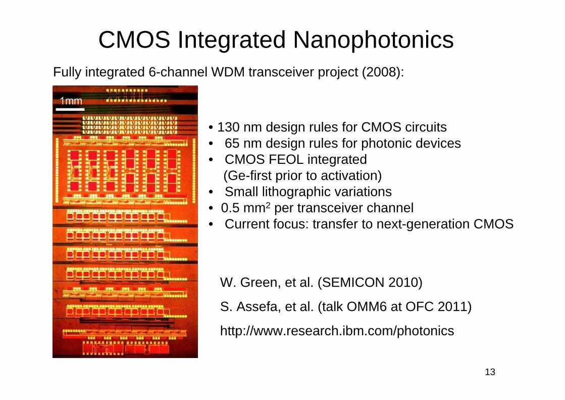
CMOS Integrated Nanophotonics
W. Green, et al. (SEMICON 2010)
S. Assefa, et al. (talk OMM6 at OFC 2011)
http://www.research.ibm.com/photonics
• 130 nm design rules for CMOS circuits• 65 nm design rules for photonic devices• CMOS FEOL integrated
(Ge-first prior to activation)• Small lithographic variations• 0.5 mm2 per transceiver channel• Current focus: transfer to next-generation CMOS
Fully integrated 6-channel WDM transceiver project (2008):
14
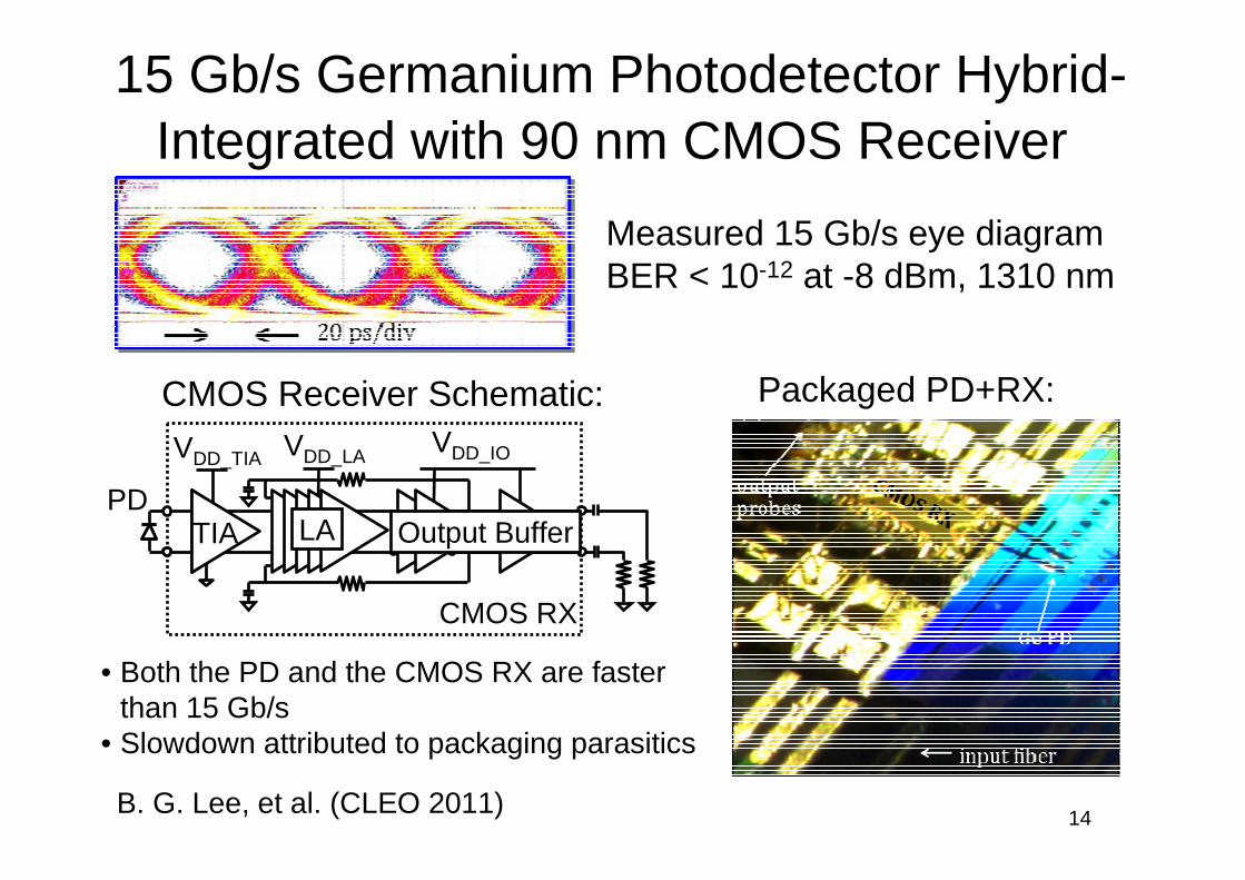
Packaged PD+RX:
15 Gb/s Germanium Photodetector Hybrid-Integrated with 90 nm CMOS Receiver
_Predriver
PD
VDD_TIA
TIA
VDD_LA VDD_IO
CMOS RX
LA Output Buffer
CMOS Receiver Schematic:
B. G. Lee, et al. (CLEO 2011)
Measured 15 Gb/s eye diagram BER < 10-12 at -8 dBm, 1310 nm
• Both the PD and the CMOS RX are faster than 15 Gb/s
• Slowdown attributed to packaging parasitics
15
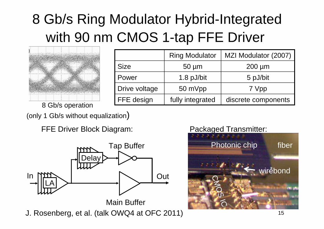
8 Gb/s Ring Modulator Hybrid-Integrated with 90 nm CMOS 1-tap FFE Driver
LA
Main Buffer
Delay
Tap Buffer
In Out
8 Gb/s operation
(only 1 Gb/s without equalization)
FFE Driver Block Diagram: Packaged Transmitter:
J. Rosenberg, et al. (talk OWQ4 at OFC 2011)
Photonic chip fiber
wirebondCM
OS
IC
7 Vpp50 mVppDrive voltage
discrete componentsfully integratedFFE design
5 pJ/bit1.8 pJ/bitPower
200 µm50 µmSize
MZI Modulator (2007)Ring Modulator
16
Outline
• Motivation• Silicon photonics technology overview• Integration strategies: full monolithic and hybrid• 4×4 switch hybrid-integrated with CMOS driver
– 2×2 switch performance– 4×4 switch architecture– Circuit and package considerations– Testing results
• Conclusion
17
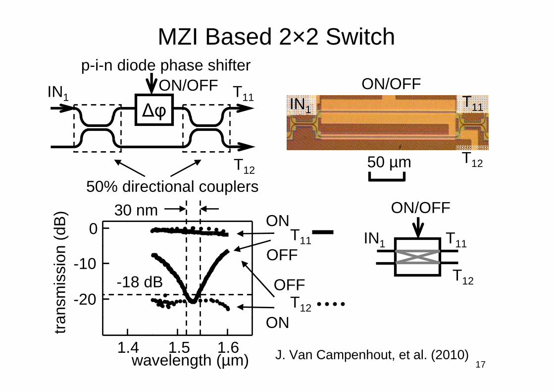
1.4 1.5 1.6
-20
-10
0
wavelength (µm)
tran
smis
sion
(dB
)
-18 dB
T11
30 nmON
OFF
T12
ON
OFF
IN1
∆φ
p-i-n diode phase shifter
IN1
50% directional couplers
T11
T12
T11
T1250 µm
T12
T11IN1
ON/OFF
ON/OFFON/OFF
MZI Based 2×2 Switch
J. Van Campenhout, et al. (2010)
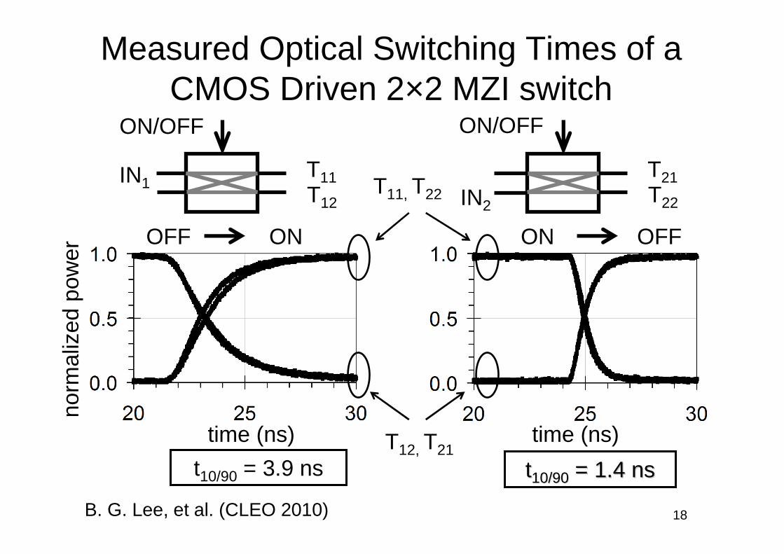
18
OFF
t10/90 = 3.9 ns tt10/9010/90 = 1.4 ns= 1.4 ns
ON ON OFF
time (ns)
norm
aliz
ed p
ower
T12, T21 time (ns)
T11, T22 T12
T11IN1
ON/OFF
T22
T21
IN2
ON/OFF
Measured Optical Switching Times of a CMOS Driven 2×2 MZI switch
B. G. Lee, et al. (CLEO 2010)
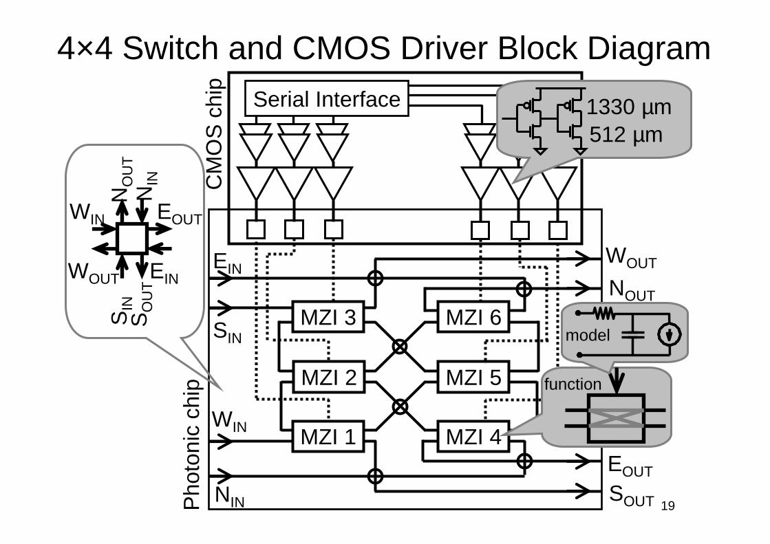
19NIN
SIN
WIN
EIN
MZI 3
MZI 2
MZI 1
MZI 6
MZI 5
MZI 4
CM
OS
chi
pP
hoto
nic
chip
WOUT
NOUT
EOUT
SOUT
NIN
NO
UT
SO
UT
SIN
WIN
WOUT
EOUT
EIN
model
function
4×4 Switch and CMOS Driver Block DiagramSerial Interface
512 µm1330 µm
20
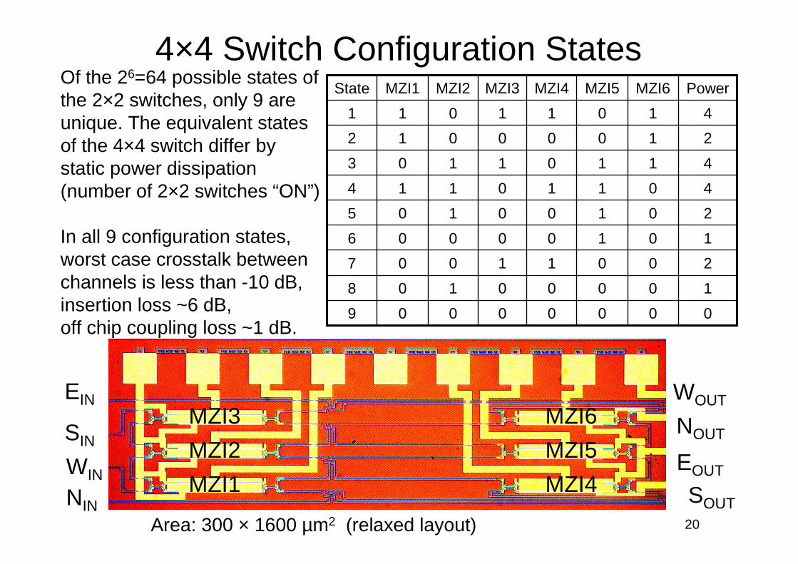
4×4 Switch Configuration States
MZI3
MZI2
MZI1
MZI6
MZI5
MZI4
0
0
1
0
0
1
0
0
1
MZI4
0
0
1
0
0
0
1
0
1
MZI3
0
1
0
0
1
1
1
0
0
MZI2
20105
40114
41103
21012
41011
PowerMZI6MZI5MZI1State
00009
10008
20007
10106
EIN
SIN
WIN
NIN
WOUT
NOUT
EOUT
SOUT
Of the 26=64 possible states of the 2×2 switches, only 9 are unique. The equivalent states of the 4×4 switch differ by static power dissipation (number of 2×2 switches “ON”)
In all 9 configuration states, worst case crosstalk between channels is less than -10 dB,insertion loss ~6 dB, off chip coupling loss ~1 dB.
Area: 300 × 1600 µm2 (relaxed layout)
21
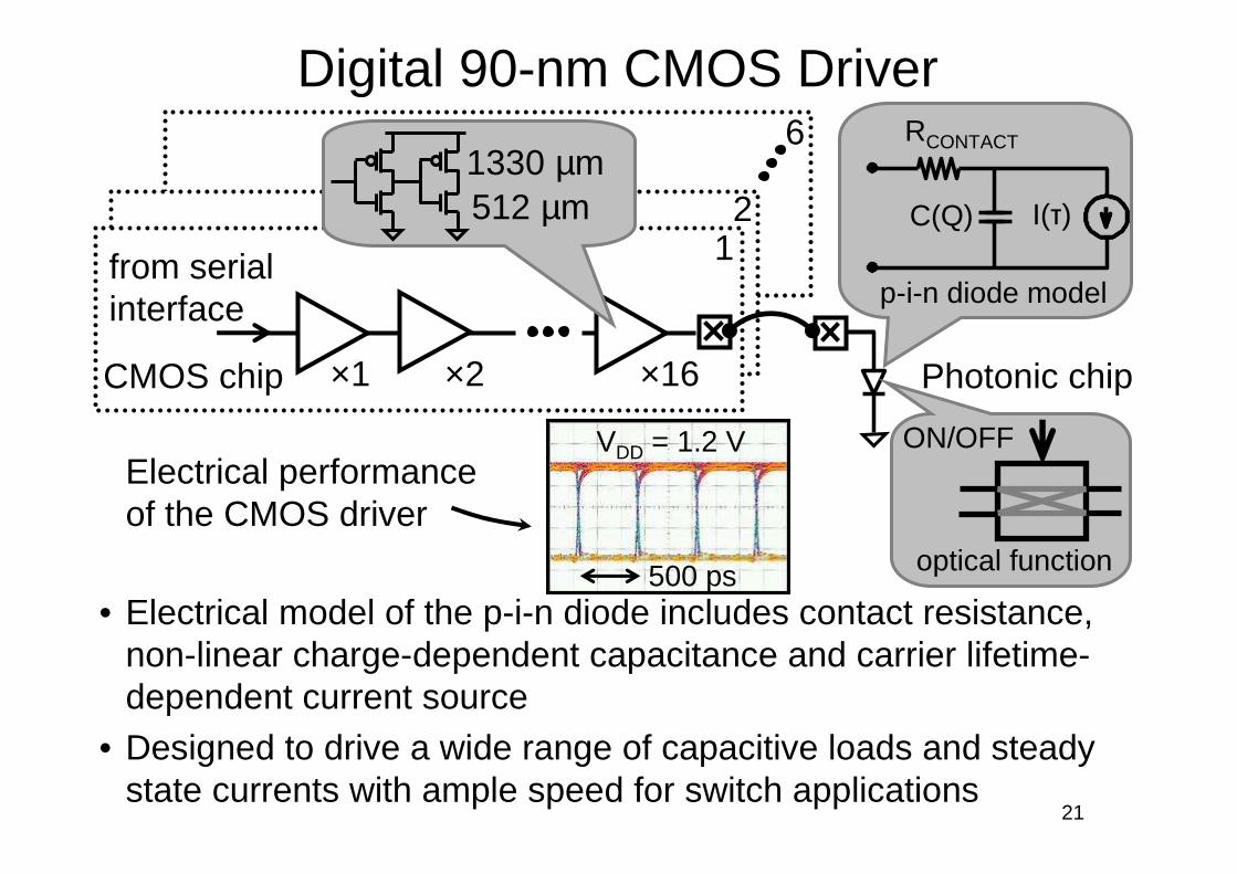
Digital 90-nm CMOS DriverRCONTACT
I(τ)C(Q)
• Electrical model of the p-i-n diode includes contact resistance, non-linear charge-dependent capacitance and carrier lifetime-dependent current source
• Designed to drive a wide range of capacitive loads and steady state currents with ample speed for switch applications
VDD = 1.2 V
500 ps
×1 ×2 ×16
from serialinterface
512 µm1330 µm
12
6
CMOS chip
p-i-n diode model
Photonic chip
ON/OFF
optical function
Electrical performance of the CMOS driver
22
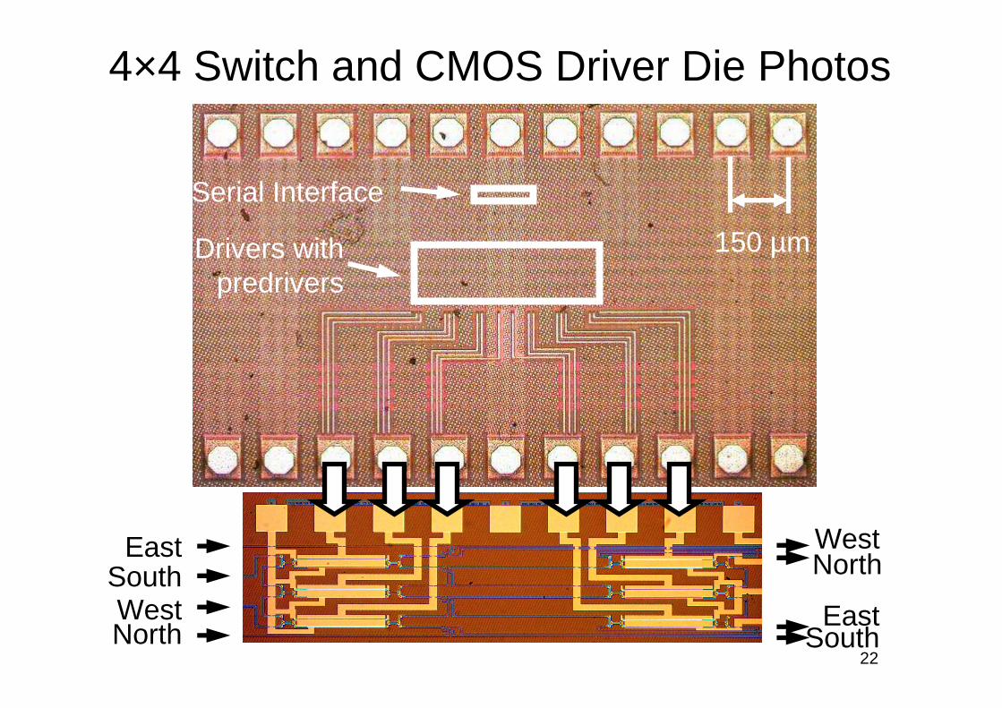
150 µm
North
SouthWest
East
South
North
East
West
Drivers with predrivers
Serial Interface
4×4 Switch and CMOS Driver Die Photos
23
CMOS IC
Photonic chip
IC probe pads on bottom
(not visible)
optical coupling
Hybrid Packaging of CMOS and Photonics
~50 µm tall
75 µm pads, 150 µm pitch
~30 µm tall
solder reflowed again to collapse columns into balls
Photonic chip pads
Ni-Au Pad Metallization:
Solder Transfer
• eutectic SnPb solder (260-300°C) plus forming gas
• ~25-30 g/bond obtained
Flux-Free Solder Process:
CMOS chip pads
24
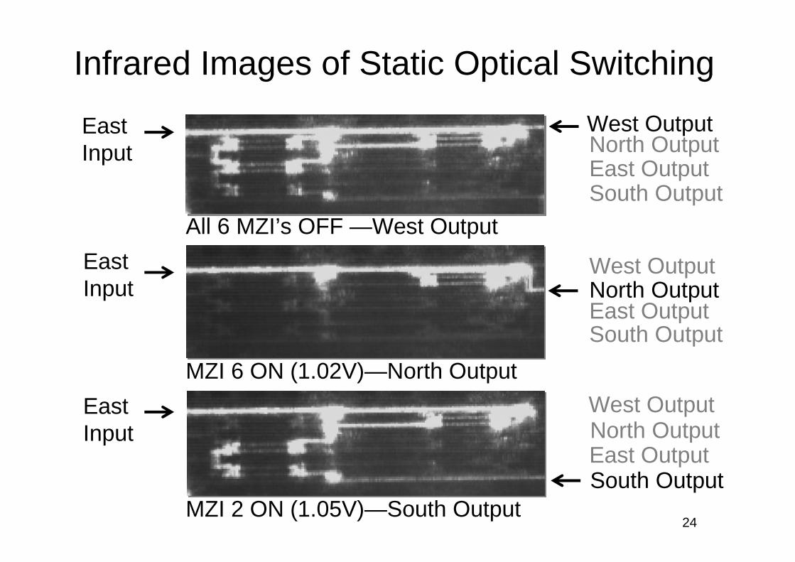
North Output
South Output
EastInput
West OutputNorth OutputEast OutputSouth Output
West Output
East OutputSouth Output
North OutputWest Output
East Output
All 6 MZI’s OFF —West Output
MZI 6 ON (1.02V)—North Output
MZI 2 ON (1.05V)—South Output
EastInput
EastInput
Infrared Images of Static Optical Switching
25
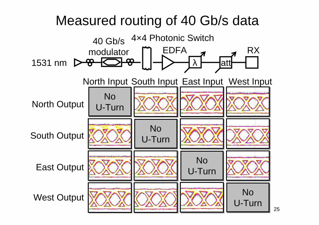
North Output
East Input
South Output
East Output
West Output
South InputNorth Input West Input
NoU-Turn
NoU-Turn
NoU-Turn
NoU-Turn
NoU-Turn
NoU-Turn
NoU-Turn
NoU-Turn
λ att1531 nm
40 Gb/smodulator RX
4×4 Photonic SwitchEDFA
Measured routing of 40 Gb/s data
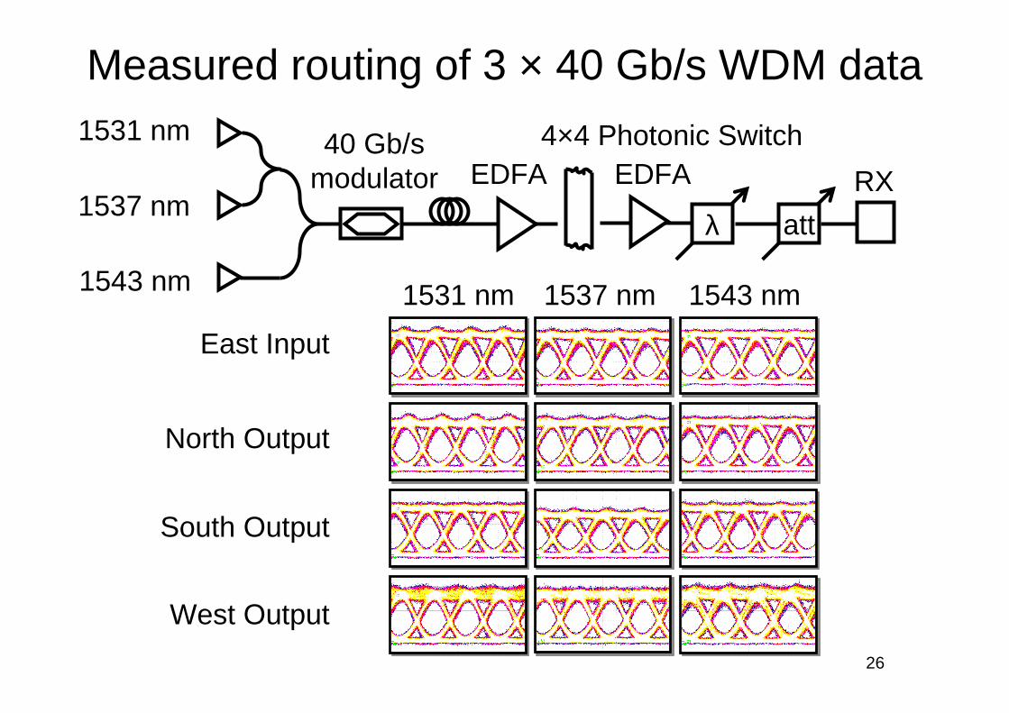
26
East Input
1543 nm
North Output
South Output
West Output
1537 nm1531 nm
40 Gb/smodulator
4×4 Photonic Switch
RX
1531 nm
1537 nm
1543 nm
EDFA EDFA
λ att
Measured routing of 3 × 40 Gb/s WDM data
27
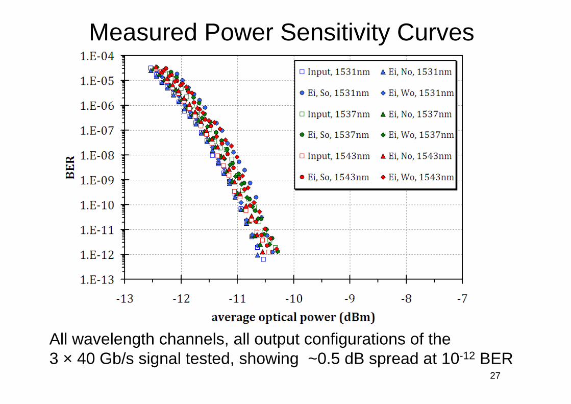
Measured Power Sensitivity Curves
All wavelength channels, all output configurations of the 3 × 40 Gb/s signal tested, showing ~0.5 dB spread at 10-12 BER
28
Conclusion• Full set of CMOS compatible photonic devices:
– waveguides, splitters, couplers, crossings, WDM structures, etc.– waveguide coupled integrated Ge photodetectors– MZI and ring based switches, modulators
• High-density, low-loss edge fiber coupling demonstrated– 8 parallel fibers coupled to on-chip waveguides on 20 µm pitch
• Monolithically integrated technology announced in December 2010
• Recent CMOS driven hybrid-integrated results include a 15 Gb/sreceiver and a ring modulator based 8 Gb/s transmitter
• Hybrid-integrated packaging process developed
• Hybrid-integrated CMOS driven 4×4 switch fully tested
The authors gratefully acknowledge support from DARPA under contract HR0011-08-C-0102.