Embed Size (px)
Citation preview
A Dynamic GHz-Band Switching Technique for RF CMOS VCO
K, Shibata. ; H, Sato. ; N, Ishihara. ;Silicon Monolithic Integrated Circuits in RF Systems, 2007 Topical Meeting on
Jan.10-12 2007 Page(s):273 - 276
積體電路設計研究所積體電路設計研究所
指導教授 指導教授 : : 林志明 教授林志明 教授
學生 學生 : : 郭峻瑋郭峻瑋
OutlineOutline
• Abstract
• Introduction
• Conventional VCO
• VCO circuit using simultaneous LC switching
• Experimental results and discussions
• Conclusion
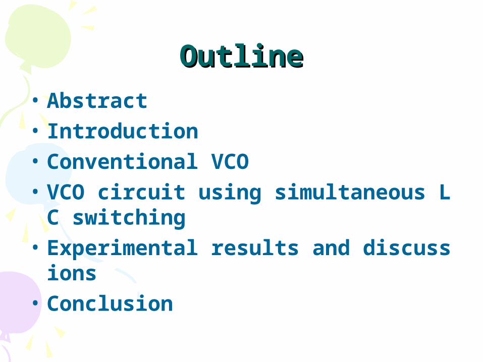
Abstract• To get wide band switching, it has been clarified a
nalytically that keeping Q constant is important to configure the circuit.
• a dual band VCO circuit has been designed by using a 0.13-μm standard CMOS process technology and succeeded in switching the band dynamically from 2 to 4 GHz .
Introduction
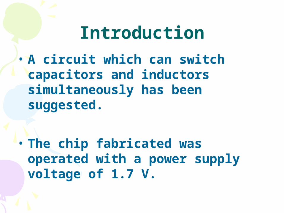
• A circuit which can switch capacitors and inductors simultaneously has been suggested.
• The chip fabricated was operated with a power supply voltage of 1.7 V.
Conventional VCOConventional VCO
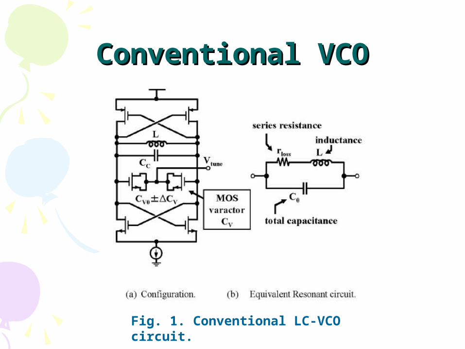
Fig. 1. Conventional LC-VCO circuit.
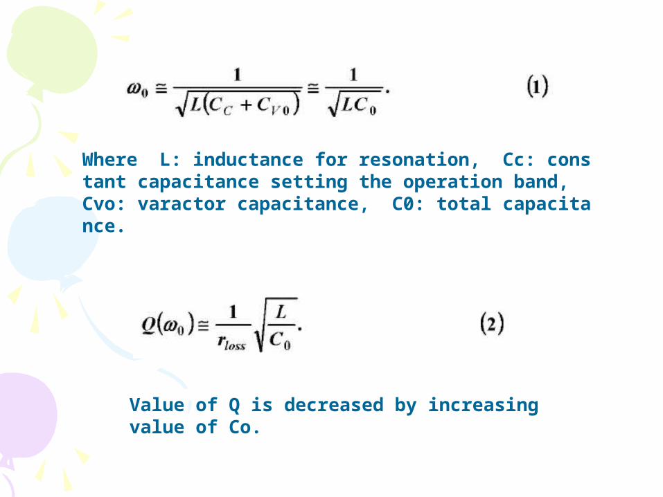
Where L: inductance for resonation, Cc: constant capacitance setting the operation band, Cvo: varactor capacitance, C0: total capacitance.
Value of Q is decreased by increasing value of Co.
VCO circuit using simultaneous VCO circuit using simultaneous LC switching LC switching
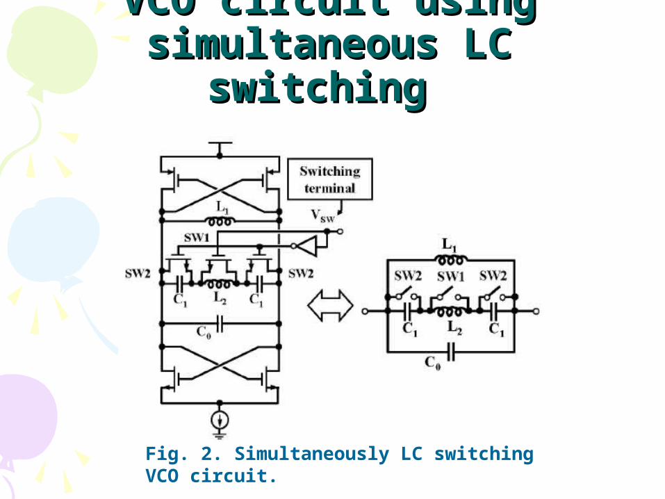
Fig. 2. Simultaneously LC switching VCO circuit.
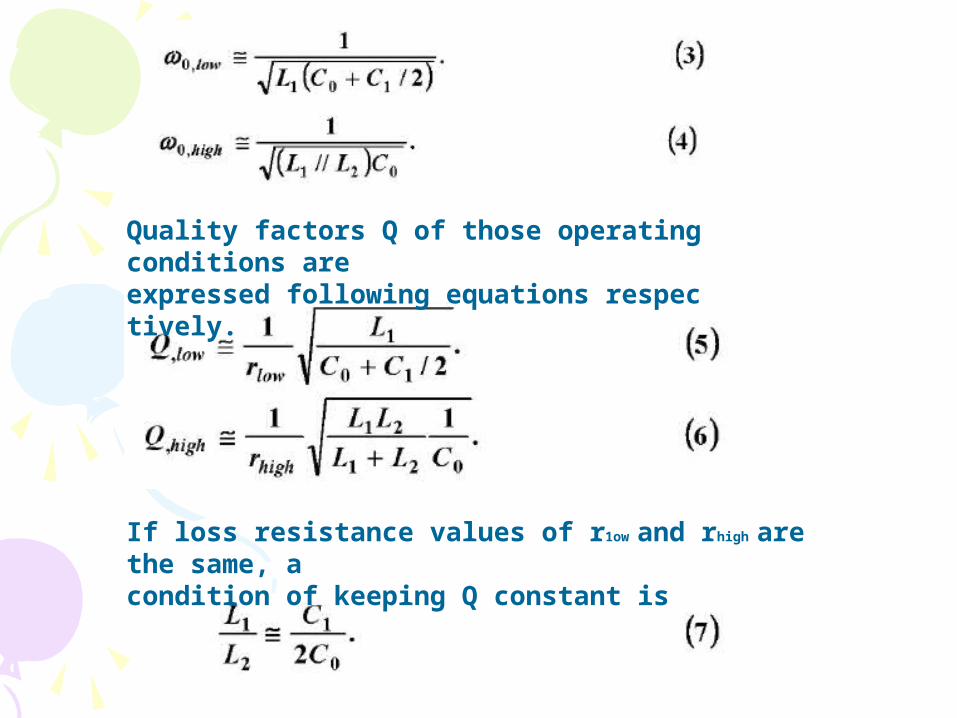
Quality factors Q of those operating conditions areexpressed following equations respectively.
If loss resistance values of r1ow and rhigh are the same, acondition of keeping Q constant is
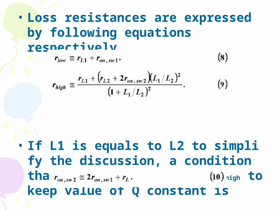
• Loss resistances are expressed by following equations respectively.
• If L1 is equals to L2 to simplify the discussion, a condition that r1ow becomes equal to rhigh to keep value of Q constant is
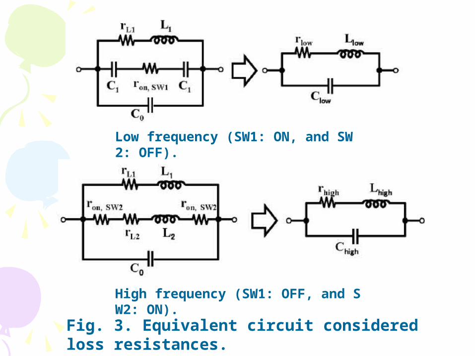
Low frequency (SW1: ON, and SW2: OFF).
High frequency (SW1: OFF, and SW2: ON).
Fig. 3. Equivalent circuit considered loss resistances.
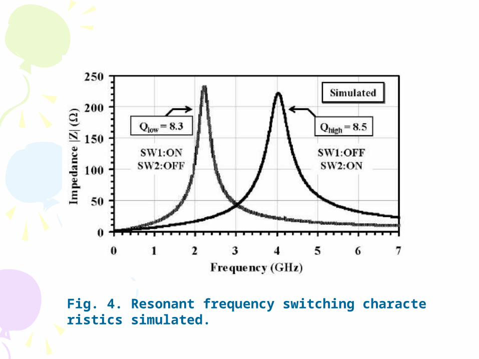
Fig. 4. Resonant frequency switching characteristics simulated.
Experimental results and Experimental results and discussionsdiscussions
• Signal output buffers which can drive 50 Ω are added to the core LC-VCO circuit.
• The sizeis 1.8 mm x 1.7 mm.
• The chip packaged was measured by using a spectrum analyzer.
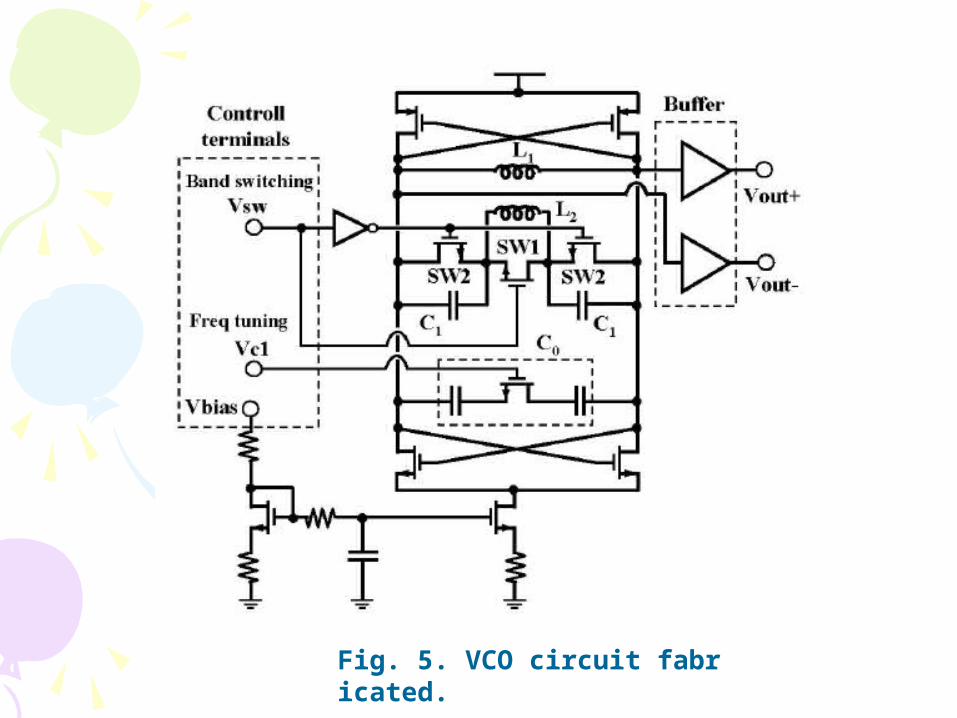
Fig. 5. VCO circuit fabricated.
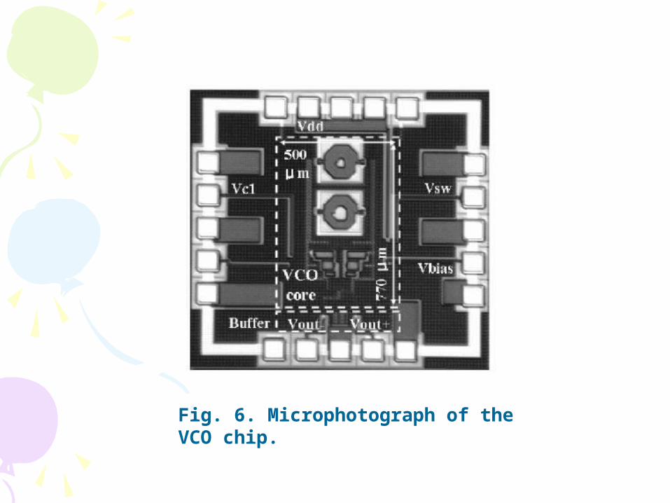
Fig. 6. Microphotograph of the VCO chip.
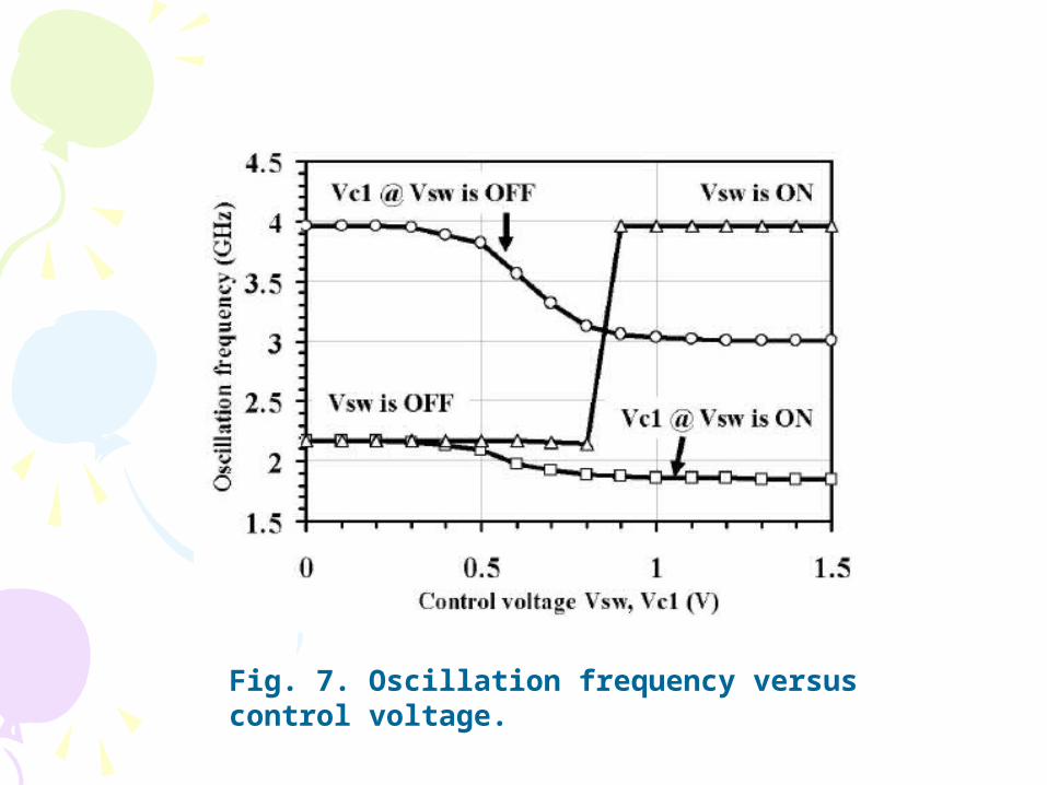
Fig. 7. Oscillation frequency versus control voltage.
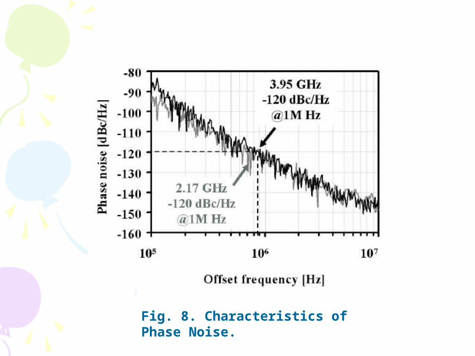
Fig. 8. Characteristics of Phase Noise.
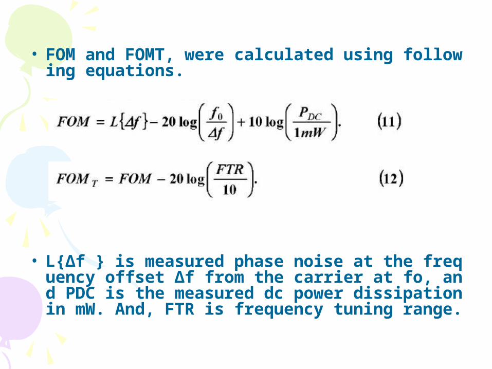
• FOM and FOMT, were calculated using following equations.
• L{Δf } is measured phase noise at the frequency offset Δf from the carrier at fo, and PDC is the measured dc power dissipation in mW. And, FTR is frequency tuning range.
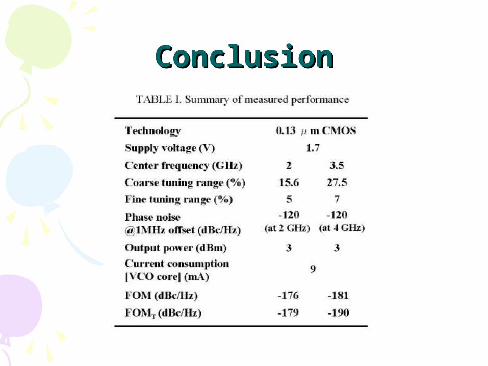
ConclusionConclusion

![Michael Vallance & Yukiko Shibata Mirai Daigaku, Japan 4-1-60.pdfThe JALT CALL Journal 2008 [Vol. 4.1] — 61. Vallance & Shibata: Effective implementation of interactive podcasting](https://img.pdfslide.tips/doc/110x75/5f2b15eaf37b49391e2ad76f/michael-vallance-yukiko-shibata-mirai-daigaku-japan-4-1-60pdf-the-jalt-call.jpg)


![Monolithic porous carbon materials prepared from ...carbonlett.org/Upload/files/CARBONLETT/[11-17]-02.pdf · 11 Monolithic porous carbon materials prepared from polyurethane foam](https://img.pdfslide.tips/doc/110x75/5af723677f8b9ae9488fb5b0/monolithic-porous-carbon-materials-prepared-from-11-17-02pdf11-monolithic.jpg)