Embed Size (px)
Citation preview

The University of Tokyo1188th Asia and South Pacific Design Automation th Asia and South Pacific Design Automation Conference, Conference, ASPASP--DAC 201DAC 20133, Yokohama, Japan, Yokohama, Japan
Xin Zhang1, Po-Hung Chen1, Yoshikatsu Ryu2, Koichi Ishida1, Yasuyuki Okuma2, Kazunori Watanabe2, Takayasu Sakurai1, and Makoto Takamiya1
A Low Voltage Buck DC-DC Converter Using On-Chip Gate Boost Technique in 40nm CMOS
1University of Tokyo, Tokyo, Japan,2Semiconductor Technology Academic Research Center (STARC), Yokohama, Japan
1The University of Tokyo1188th Asia and South Pacific Design Automation th Asia and South Pacific Design Automation Conference, Conference, ASPASP--DAC 201DAC 20133, Yokohama, Japan, Yokohama, Japan
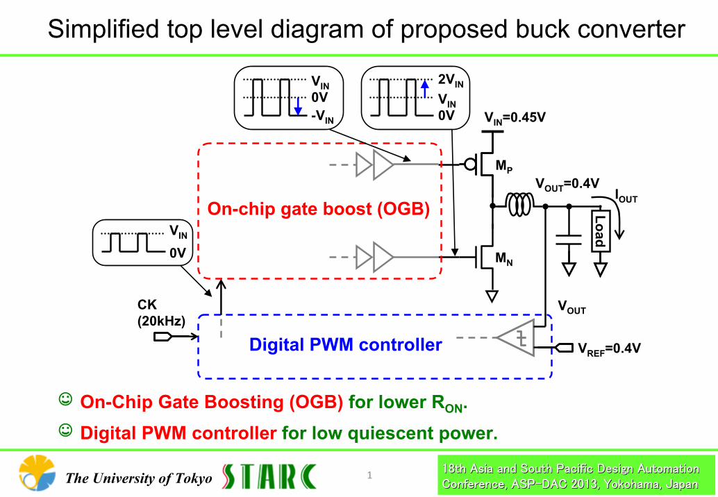
Simplified top level diagram of proposed buck converter
VIN=0.45VLoad
CK(20kHz)
VOUT=0.4V
VREF=0.4V
On-chip gate boost (OGB)IOUT
VIN
0V
VIN0V-VIN
VIN0V
2VIN
MP
MN
Digital PWM controller
VOUT
☺ On-Chip Gate Boosting (OGB) for lower RON.☺ Digital PWM controller for low quiescent power.
2The University of Tokyo1188th Asia and South Pacific Design Automation th Asia and South Pacific Design Automation Conference, Conference, ASPASP--DAC 201DAC 20133, Yokohama, Japan, Yokohama, Japan
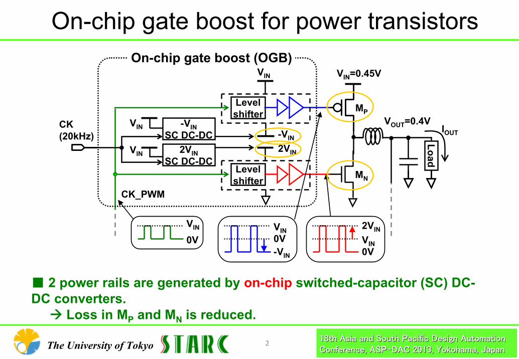
On-chip gate boost for power transistors
VIN=0.45VLoad
CK(20kHz)
VOUT=0.4V
Level shifter
-VINSC DC-DC
Level shifter
2VINSC DC-DC
VIN
-VIN
2VIN
VIN
VIN
On-chip gate boost (OGB)
IOUT
VIN
0VVIN0V-VIN
VIN0V
2VIN
CK_PWM
MP
MN
■ 2 power rails are generated by on-chip switched-capacitor (SC) DC-DC converters.
Loss in MP and MN is reduced.
3The University of Tokyo1188th Asia and South Pacific Design Automation th Asia and South Pacific Design Automation Conference, Conference, ASPASP--DAC 201DAC 20133, Yokohama, Japan, Yokohama, Japan
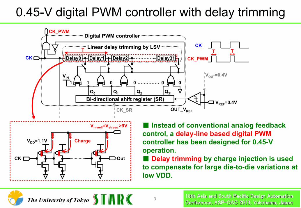
0.45-V digital PWM controller with delay trimming
CK Delay0 Delay1 Delay2 Delay31
VIN
1 1 0 0 0 0
Q0 Q1 Q2 Q31
Bi-directional shift register (SR)
OUT_VREF
Linear delay trimming by LSV
Digital PWM controller
T
CK_PWM
VREF=0.4V
VOUT=0.4V
CK_SR
T TCK
CK_PWM
VDD=1.1V
Vn-well=Vstress >9V
CK Out
Charge
■ Instead of conventional analog feedback control, a delay-line based digital PWMcontroller has been designed for 0.45-V operation.■ Delay trimming by charge injection is used to compensate for large die-to-die variations at low VDD.
4The University of Tokyo1188th Asia and South Pacific Design Automation th Asia and South Pacific Design Automation Conference, Conference, ASPASP--DAC 201DAC 20133, Yokohama, Japan, Yokohama, Japan
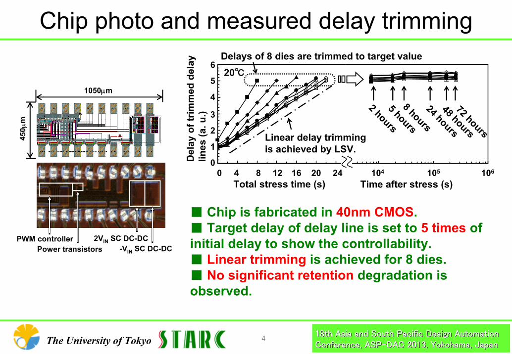
Chip photo and measured delay trimming
0
1
2
3
4
5
6
Linear delay trimming is achieved by LSV.
Delays of 8 dies are trimmed to target value
2 hours5 hours8 hours24 hours48 hours
1
2
3
4
5
6
0Del
ay o
f trim
med
del
ay
lines
(a. u
.)
0 4 8 12 16 20 24 104 105 106
Total stress time (s) Time after stress (s)
72 hours
20℃
1050μm
450μ
m
PWM controllerPower transistors -VIN SC DC-DC
2VIN SC DC-DC
■ Chip is fabricated in 40nm CMOS.■ Target delay of delay line is set to 5 times of initial delay to show the controllability.■ Linear trimming is achieved for 8 dies. ■ No significant retention degradation is observed.
5The University of Tokyo1188th Asia and South Pacific Design Automation th Asia and South Pacific Design Automation Conference, Conference, ASPASP--DAC 201DAC 20133, Yokohama, Japan, Yokohama, Japan
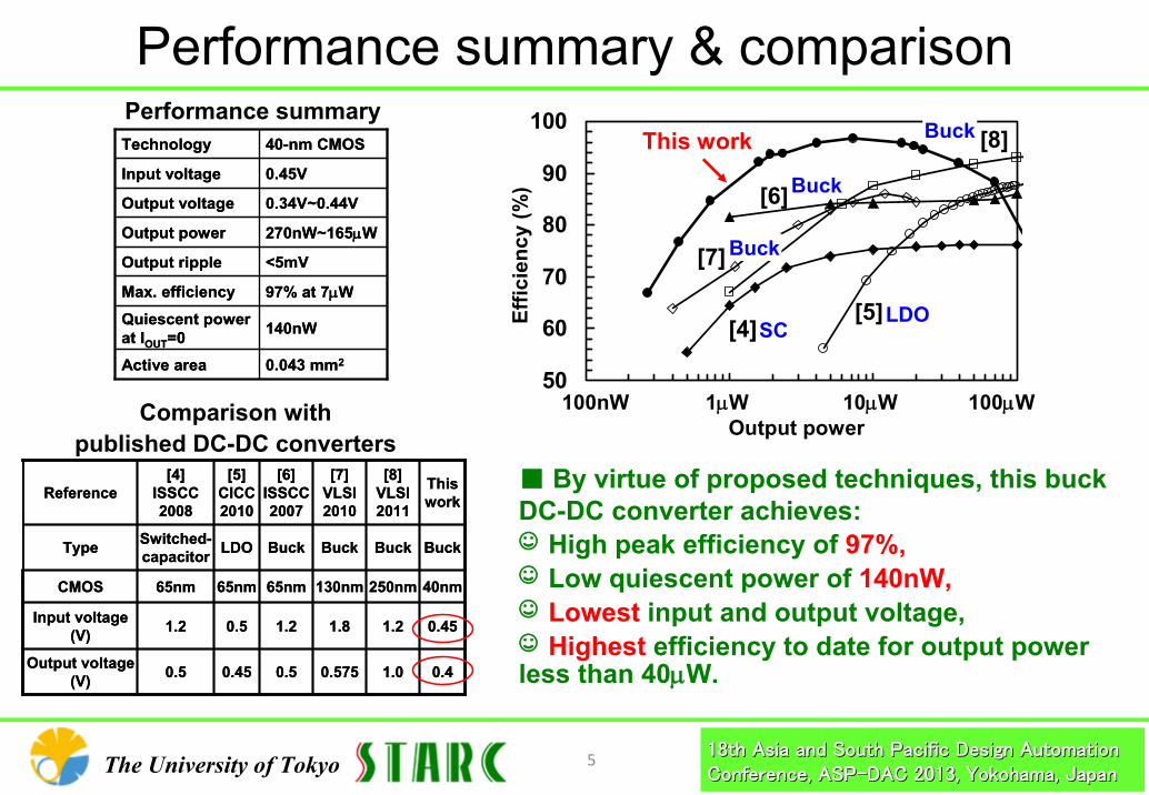
Performance summary & comparison
50
60
70
80
90
100
Effic
ienc
y (%
)
100nW 1μW 10μW 100μW
[4][5]
[6]
[7]
[8]This work
Output power
Buck
Buck
Buck
LDOSC
■ By virtue of proposed techniques, this buck DC-DC converter achieves:☺ High peak efficiency of 97%,☺ Low quiescent power of 140nW,☺ Lowest input and output voltage,☺ Highest efficiency to date for output power less than 40μW.0.5
1.2
65nm
Switched-capacitor
[4] ISSCC 2008
0.45
0.5
65nm
LDO
[5] CICC2010
0.5
1.2
65nm
Buck
[6] ISSCC 2007
0.575
1.8
130nm
Buck
[7] VLSI 2010
1.0
1.2
250nm
Buck
[8] VLSI 2011
0.4Output voltage(V)
0.45Input voltage(V)
40nmCMOS
BuckType
This workReference
0.5
1.2
65nm
Switched-capacitor
[4] ISSCC 2008
0.45
0.5
65nm
LDO
[5] CICC2010
0.5
1.2
65nm
Buck
[6] ISSCC 2007
0.575
1.8
130nm
Buck
[7] VLSI 2010
1.0
1.2
250nm
Buck
[8] VLSI 2011
0.4Output voltage(V)
0.45Input voltage(V)
40nmCMOS
BuckType
This workReference
Performance summary
Comparison with published DC-DC converters
140nWQuiescent power at IOUT=0
0.043 mm2Active area
97% at 7μWMax. efficiency
<5mVOutput ripple
270nW~165μWOutput power
0.34V~0.44VOutput voltage
0.45VInput voltage
40-nm CMOSTechnology
140nWQuiescent power at IOUT=0
0.043 mm2Active area
97% at 7μWMax. efficiency
<5mVOutput ripple
270nW~165μWOutput power
0.34V~0.44VOutput voltage
0.45VInput voltage
40-nm CMOSTechnology