Embed Size (px)
Citation preview

OPTICAL INSTRUMENTATION AND TECHNOLOGY
A series of silicon multiplexers for HgCdTe photodiodes of the 8–16-�m spectralrange
A. I. Kozlov,a� I. V. Marchishin, V. N. Ovsyuk, and A. L. Aseev
Semiconductor Physics Institute, Siberian Branch, Russian Academy of Sciences, Novosibirsk�Submitted June 13, 2007�Opticheski� Zhurnal, 75, 60–67 �March 2008�
This paper presents the results of the development of linear �1�288, 1�576� and two-dimensional �128�128, 320�256� silicon multiplexer arrays for HgCdTe photodiodes of the8–16 �m spectral range. Typical parameters of the multiplexers are given, along with the char-acteristics of long-wavelength hybrid IR photodetectors created at the Institute of SemiconductorPhysics of the Siberian Section of the Russian Academy of Sciences. © 2008 Optical Society ofAmerica.
INTRODUCTION
In many cases that are important in practice, it is neces-sary to record images of objects and scenes in the 8–16-�mIR range. Infrared photodetector devices �PDDs� based onthe compound mercury-cadmium telluride �HgCdTe� aremost often used for this purpose.1,2
An IR PDD is most often based on a linear or two-dimensional photodetector array that is a hybrid combinationof two chips, one of which contains photosensitive elements�PSEs�, while the second contains an integrated multiplexercircuit that counts the electrical signals after photoelectricconversion of IR radiation in the PSEs, eliminating or sim-plifying mechanical scanning over one or over twocoordinates.1–3
Photodiodes based on HgCdTe compounds for the far IRregion �8–16-�m� are characterized by large dark and/orbackground currents, by the presence of excess 1 / f noise,and by rigorous requirements on the homogeneity of the biasvoltages.2,4
The leading firms �Sofradir, Indigo Systems Corp., etc.�have developed and are currently commercially producingstandardized series of linear �4�288, 6�460, 1�512� andtwo-dimensional �128�128, 320�240, 320�256, 384�288, 640�512� silicon multiplexer arrays for photodetec-tors of the far-, mid-, and near-IR regions.5,6 Rockwell Sci-ence Center has proposed, for example, more than twentymodels of multiplexers for HgCdTe photodiodes in spectralranges from 1.05 to 14 �m. The models differ from eachother in format, input circuits, charge capacity, and the stepof the cells. It should be pointed out that the maximum for-mat of the arrays decreases as the working wavelength of thephotodetector increases: 2048�2048 resolution elements forthe spectral range 0.9–2.5 �m, 1024�1024 for the0.9–5.0-�m range, 256�256 for the 8–12-�m range, andonly 128�128 for the 8–14-�m range.
This paper discusses questions of the creation of a stan-dardized series of multiplexers intended for the readout andpreprocessing of photosignals with linear �1�128, 1�576�and two-dimensional �128�128, 320�256� HgCdTe photo-detector arrays of the 8–16-�m spectral range. The multi-
187 J. Opt. Technol. 75 �3�, March 2008 1070-9762/2008/03
plexers were developed at the Institute of SemiconductorPhysics of the Siberian Section of the Russian Academy ofSciences �IFP SO RAN� and are fabricated using CMOStechnology on the manufacturing base of OAO Angstrem.
A feature of the multiplexers considered here is a largeprogrammable accumulation capacitor, with a maximumoverall charge of up to 48 pC, and this allows the IR PDDsto operate in the 8–16-�m spectral range under variousbaseline conditions.
TWO-DIMENSIONAL MULTIPLEXER ARRAYS
General principles of organization
For HgCdTe photodiodes with low dark currents Idark
and high differential resistances Rd, ordinary modern multi-plexers can be used with moderate accumulation capacitorsCacc located in each cell of the array. An example is providedby an IR PDD based on a HgCdTe-photodiode array withlong-wavelength sensitivity limit �OTC=10.3 �m, dark cur-rent Idark=0.7 nA, and differential resistance Rd=1010 � at atemperature of 78 K.7 In this case, Cacc=7.9 pC, located ineach cell of the array, was sufficient to achieve high detec-tivities and good temperature resolution; the accumulationtime was limited to 200 �s.8
To implement the required detectivities with IR PDDsbased on HgCdTe photodiodes characterized by higher ther-mal currents and under conditions of significant backgroundcurrents, it is necessary to use large accumulation capacitors,which can be obtained by using an alternative principle ofoff-pixel or linewise accumulation.9–14 Such a linewise-accumulation multiplexer array �LAMA� usually consists ofan array of switches and a set of readout channels includinginput photocurrent-readout circuits, accumulation capacitors,and amplifiers at the output. The channels are serially multi-plexed to a common output by means of an addressingscheme. A silicon multiplexer for linear photodetector arrayshas such a structure, composed of a set of readoutchannels.15,16
A functional layout of the LAMA 320�256 that wasdeveloped is shown in Fig. 1. The multiplexer consists of an
1870187-07$15.00 © 2008 Optical Society of America
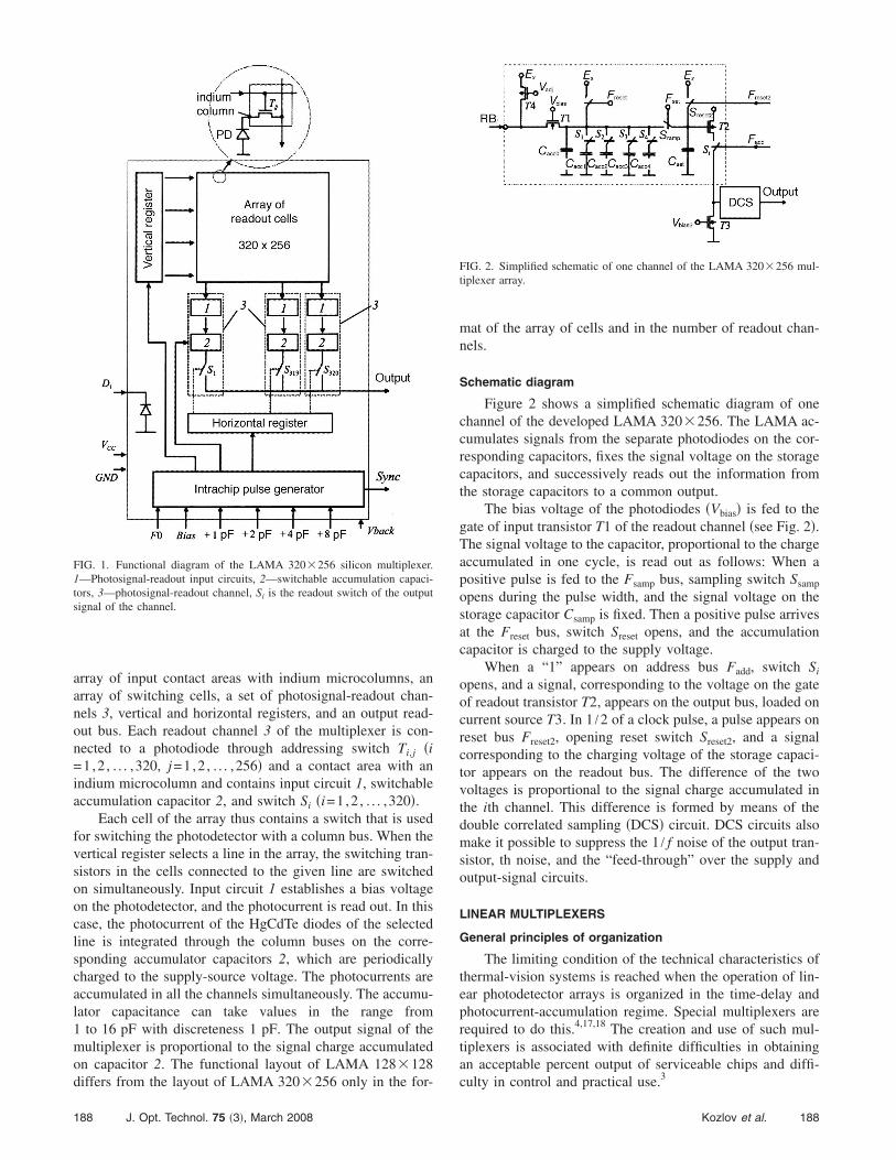
array of input contact areas with indium microcolumns, anarray of switching cells, a set of photosignal-readout chan-nels 3, vertical and horizontal registers, and an output read-out bus. Each readout channel 3 of the multiplexer is con-nected to a photodiode through addressing switch Ti,j �i=1,2 , . . . ,320, j=1,2 , . . . ,256� and a contact area with anindium microcolumn and contains input circuit 1, switchableaccumulation capacitor 2, and switch Si �i=1,2 , . . . ,320�.
Each cell of the array thus contains a switch that is usedfor switching the photodetector with a column bus. When thevertical register selects a line in the array, the switching tran-sistors in the cells connected to the given line are switchedon simultaneously. Input circuit 1 establishes a bias voltageon the photodetector, and the photocurrent is read out. In thiscase, the photocurrent of the HgCdTe diodes of the selectedline is integrated through the column buses on the corre-sponding accumulator capacitors 2, which are periodicallycharged to the supply-source voltage. The photocurrents areaccumulated in all the channels simultaneously. The accumu-lator capacitance can take values in the range from1 to 16 pF with discreteness 1 pF. The output signal of themultiplexer is proportional to the signal charge accumulatedon capacitor 2. The functional layout of LAMA 128�128differs from the layout of LAMA 320�256 only in the for-
FIG. 1. Functional diagram of the LAMA 320�256 silicon multiplexer.1—Photosignal-readout input circuits, 2—switchable accumulation capaci-tors, 3—photosignal-readout channel, Si is the readout switch of the outputsignal of the channel.
188 J. Opt. Technol. 75 �3�, March 2008
mat of the array of cells and in the number of readout chan-nels.
Schematic diagram
Figure 2 shows a simplified schematic diagram of onechannel of the developed LAMA 320�256. The LAMA ac-cumulates signals from the separate photodiodes on the cor-responding capacitors, fixes the signal voltage on the storagecapacitors, and successively reads out the information fromthe storage capacitors to a common output.
The bias voltage of the photodiodes �Vbias� is fed to thegate of input transistor T1 of the readout channel �see Fig. 2�.The signal voltage to the capacitor, proportional to the chargeaccumulated in one cycle, is read out as follows: When apositive pulse is fed to the Fsamp bus, sampling switch Ssamp
opens during the pulse width, and the signal voltage on thestorage capacitor Csamp is fixed. Then a positive pulse arrivesat the Freset bus, switch Sreset opens, and the accumulationcapacitor is charged to the supply voltage.
When a “1” appears on address bus Fadd, switch Si
opens, and a signal, corresponding to the voltage on the gateof readout transistor T2, appears on the output bus, loaded oncurrent source T3. In 1 /2 of a clock pulse, a pulse appears onreset bus Freset2, opening reset switch Sreset2, and a signalcorresponding to the charging voltage of the storage capaci-tor appears on the readout bus. The difference of the twovoltages is proportional to the signal charge accumulated inthe ith channel. This difference is formed by means of thedouble correlated sampling �DCS� circuit. DCS circuits alsomake it possible to suppress the 1 / f noise of the output tran-sistor, th noise, and the “feed-through” over the supply andoutput-signal circuits.
LINEAR MULTIPLEXERS
General principles of organization
The limiting condition of the technical characteristics ofthermal-vision systems is reached when the operation of lin-ear photodetector arrays is organized in the time-delay andphotocurrent-accumulation regime. Special multiplexers arerequired to do this.4,17,18 The creation and use of such mul-tiplexers is associated with definite difficulties in obtainingan acceptable percent output of serviceable chips and diffi-culty in control and practical use.3
FIG. 2. Simplified schematic of one channel of the LAMA 320�256 mul-tiplexer array.
188Kozlov et al.

is the
When it is not required to achieve the limiting charac-teristics of the IR PDDs and/or when the level of fabricationtechnology of a multielement photosensitive structure is suit-able, it can be economically expedient to use hybrid photo-detectors with a single-row arrangement of the PSEs, whichis provided by simple 1�576 and 1�288 linear multiplex-ers �LMs�. Moreover, the latter is available in the format ofthe Sofradir photodetectors, has a reduced power require-ment, and ensures a high percentage yield of serviceablechips during fabrication.
There is special interest in fairly long 1�576LMs,4,15,16,18,19 which make it possible to completely elimi-nate mechanical scanning over one of the coordinates whenforming full-format �768�576� IR images.
The functional layout of the developed 1�576 multi-plexers �common to LM-1 and LM-2� is shown in Fig. 3.The multiplexer consists of input contact areas 1 with indiummicrocolumns, a set of photosignal-readout channels 4, fourbias resistors, and four output readout buses. Each readoutchannel of the multiplexer is directly connected to a photo-diode through contact area 1 with an indium microcolumnand contains input circuit 2, switchable accumulation capaci-tor 3, an active source-follower transistor, and switch Si �i=1,2 , . . . ,576�.
A bias voltage is established on the photodetector bymeans of input circuit 2, and the photocurrent is read out.The photocurrent is integrated on accumulator capacitor 3,which is periodically charged to the supply-source voltage. A
FIG. 3. Functional diagram of a 1�576 silicon multiplexer. 1—Input co3—switchable accumulation capacitors, 4—photosignal-readout channel, Si
189 J. Opt. Technol. 75 �3�, March 2008
pulse with high logical level “1” moves along the bias reg-ister, which is controlled by pulsed voltages. The differenceof the charging and discharging levels of each capacitor 3 isfixed once per polling period of all the readout channels andis transmitted to the output by means of address switch Si.
Schematic diagrams
Figure 4 shows a standardized schematic diagram of onechannel of the 576-channel multiplexer LM-2 that has beencreated.
areas with indium microcolumns, 2—input photosignal-readout circuits,readout switch of the output signal of the channel.
FIG. 4. Standardized schematic of one channel of the LM-2 1�576 linearmultiplexer.
ntact
189Kozlov et al.

The signal voltage on a capacitor, proportional to thecharge accumulated in one cycle, is read out as follows:16
When a “1” appears on address bus Fadd, switch Si opens,and a signal that corresponds to the voltage on the gate ofreadout transistor T2 appears on the output bus loaded ontocurrent source T3. Every 1 /2 of a clock period, a pulse ap-pears on reset bus Freset that opens reset switch Sreset, and asignal appears on the readout bus that corresponds to thecapacitor-charging voltage. The difference of the two volt-ages is proportional to the signal charge accumulated in theith channel. This difference is formed by means of the DCScircuit.
The differential amplifier in this circuit, besides the func-tion of forming an accurate, thermally stable bias, ensuresthat the readout circuit has a low input resistance. The pa-rameters of the transistors of the differential cascade werechosen from the condition that the noise is minimized whenthe required current is small. The minimum detector resis-tance that provides the multiplexer-readout regime withnoise limited by the fluctuations of the background flux of IRradiation, is about 200 k� when the accumulation time istacc=40 �s.
The schematic diagram of a channel of multiplexerLM-1 differs only in that there is no differential amplifier.The bias voltage of the photodiodes is supplied directly tothe gate of the input transistor �T1� of the readout channel.The signal voltage on the capacitor, proportional to thecharge accumulated in one cycle, is read out in the same wayas that considered above. It should be pointed out that, bycomparison with multiplexer LM-2, the distinguishing fea-ture of multiplexer LM-1 is a lower power requirement.
Multiplexer LM 1�288 is made using the circuit ofmultiplexer LM-1 in the format of the Sofradir photodetec-tors, with a 28-�m step.
The linear multiplexers LM, LM-1, and LM-2 that havebeen developed are convenient to care for, since they requireonly two constant-voltage sources for operation: the supplyvoltage �+Es� and the accurately adjusted reverse bias of thephotodiode �Vbias�, as well as three pulsed voltages for con-trolling the recording of the shift.
INPUT PHOTOSIGNAL-READOUT CIRCUITS
The input circuits of the multiplexers must satisfy manyrequirements. It is especially important in our case for themto be highly homogeneous in the photodetector bias and thephotocurrent-readout efficiency.1
When a simple circuit for directly injecting the photo-current through a MOS transistor �multiplexers LM, LM-1,and LAMA� is used at the input, the photodiode-bias inho-mogeneity repeats the threshold-voltage inhomogeneity ofthe input MOS transistors.20 The characteristic inhomogene-ity of the threshold voltage of the multiplexer’s input tran-sistors when the integrated circuits are fabricated by moderncommercial CMOS technology is �15 mV �absolute devia-tion�.
When it is necessary to improve the bias homogeneity,the correlation property of the electrical parameters of twoadjacent transistors is used. A buffered direct-injection circuit
190 J. Opt. Technol. 75 �3�, March 2008
�multiplexer LM-2� forms the bias on the photosensor withan error equal to the difference of threshold voltages of twoadjacent transistors. This circuit uses the symmetry of thedifferential-cascade transistors of the op-amp.21,22 The inho-mogeneity of the bias voltage on the photodetectors does notexceed �6 mV when a circuit with a buffer amplifier is usedat the input.
We next consider the photocurrent-readout efficiency.Part of the photocurrent is shunted by the internal resistanceof the detector or, at high frequency, by the capacitance ofthe input module and does not reach the accumulation ca-pacitor. The photocurrent-readout efficiency is characterizedby the fraction of photocurrent injected into the device. Thecondition for high readout efficiency is the requirement
gsRd � 1, �1�
where gs is the differential conductivity of the input MOStransistor, and Rd is the differential resistance of thedetector.16
In a circuit with direct injection, the differential conduc-tivity of the input transistor depends on current I through thetransistor. The following formula can be used as an estimatein the subthreshold regime:
gs =qI
kT,
where kT /q is the thermal potential. In the above-thresholdregime, the formula is
gs =�2W
L�CoxI ,
where W /L is the width-to-length ratio of the transistor chan-nel, � is the mobility, and Cox is the specific capacitance ofthe dielectric.16
No problem with the photocurrent-readout efficiency ap-pears in our case when there is a large dark current of thedetector and/or a high IR background level.2 In order to en-sure that the photocurrent-readout efficiency at high fre-quency is sufficient, the time constant of the input modulemust be less than the time to integrate the photocurrent in themultiplexer.
The circuit with an op-amp �multiplexer LM-2�, charac-terized by a voltage gain of KV, has a factor of �KV+1�greater input conductivity for the same current through theinput transistor. The limitations imposed by inequality �1� areweakened and the circuit is more workable in the region oflower detector resistances and lower products Iptacc, where Ip
is the photocurrent and tacc is the accumulation time.2,16
Multiplexers LM 1�288, LAMA 128�128, andLAMA 320�256 allow the possibility of subtracting �com-pensating� a constant input current by using controllablesources of inverse current, located in each readout channel.The organization of the array multiplexers provides subtrac-tion of the constant input current individually for each line ofphotosensitive elements of the array. It should be kept inmind in this case that the noise of the input cascades of themultiplexers is increased by a factor of �2 because of thecurrent-subtraction regime at the input.
190Kozlov et al.

EXPERIMENTAL DATA
The multiplexers that have been developed are intendedfor combined operation with linear arrays and two-dimensional arrays of n+–p photodiodes based on HgCdTe inIR ranges 3–5 and 8–16 �m.
The multiplexers are fabricated by standard CMOS tech-nology with one layer of polysilicon gates and two layers ofmetallic leads, and with a maximum supply voltage of 6 V.
The main parameters of these multiplexers, shown inTable I, correspond to the world level. The multiplexers op-erate in a wide temperature range from 300 to 65 K and pro-vide high homogeneity of the bias voltages of the photode-tectors. The latter is especially important, since the excess1 / f noise of long-wavelength HgCdTe photodiodes is mini-mal in a narrow range of reverse biases �25–50 mV�.2,4,16,18
The main parameters were obtained by tracking an entireseries of samples and can be regarded as typical.
Although the multiplexers thus created are oriented to-ward switching to linear arrays and two-dimensional arrays
TABLE I. Main parameters of multiplexers developed for IR PD
Type of chip
Name of parameter LM 1�288 LM-1 1�
Format of chip 1�288 1�576Number of readout lines 288 576Types of photodetectorsInput polarity of photodiodesStep of input contact
areas, �m28 30
Technology 1.0 KPOP DM 1.2 KPOPType of input circuit Direct injection Direct injec
Homogeneity of bias ofphotodiodes, no worse than, mV
+15 +15
Accumulation principle � �
Subtraction of constant level ofaccumulation capacitance, pF
� �
Cacc0 1 1.3Cacc1 1 2Cacc2 2 6Cacc3 4 �
Cacc4 8 �
Maximum input current,no less than, nA
300 200
Accumulation time, �s 20 40Clock frequency, MHz 3.5 3.5Maximum output signal
no less than, V2 1.9
Dynamic range,no less than, dB
80 79
Number of signal outputs 4 4Number of working readout
cells, no less than, %100 100
Power required,no greater than, mW
30 50
Geometrical dimensions ofthe chip, mm
5.3�9.7 4�18
191 J. Opt. Technol. 75 �3�, March 2008
of IR photodiodes of the spectral ranges 3–5 and 8–16 �m,they can be used when working with photoresistors or othersignal sources.
MULTIELEMENT HYBRID PHOTODETECTORS
Based on the silicon chips of the multiplexers developedat IFP CO RAN, a whole series of linear and two-dimensional photodetector arrays has been created for thelong-wavelength IR region. The characteristics of some ofthese photodetectors are shown in Table II.3,4 It can be seenfrom the table that the 1�576 linear photodetectors, basedon LM-1 multiplexers, allow full-format high-resolutionthermal-vision systems to be created. General-purpose mul-tiplexer MM-V, described in detail in Ref. 23, with a widerange of adjustment of the accumulation time of40–20 000 �s, allows mid- and long-wavelength photode-tector arrays made from various semiconductor materials tobe operated with a working temperature from 65 to 215 K.Linewise-accumulation multiplexers LAMA 128�128 and
the 8–16-�m spectral region.
LM-2 1�576 LAMA 128�128 LAMA 320�256
1�576 128�128 320�256576 128 256
HgCdTe 8–16, 3–5 �mn+ on p substrate
30 40�40 35�35
1.2 KPOP DM 1.2 KPOP DM 1.0 KPOP DMBuffered
direct injectionDirect injection Direct injection
�6 �11 �15
� Linewise Linewise� � �
1.3 1 12 1 16 2 2� 4 4� 8 8
200 300 300
40 10–130 10–1303.5 1 2.51.9 1.9 2
79 80 80
4 1 1.4100 99 99.99
80 40 100
5�18 8.2�9.0 12.4�14.1
Ds of
576
DMtion
191Kozlov et al.

LAMA 320�256 possess large charge capacity and high dy-namic range, and this makes it possible to obtain the limitingtemperature sensitivity parameters for arrays in the8–16-�m range based on HgCdTe photodiodes.
Figure 5 shows examples of thermal images obtained inthe 8–16-�m spectral range on the basis of HgCdTe photo-diodes and silicon multiplexer LAMA 320�256.18
CONCLUSION
The Institute of Semiconductor Physics of the SiberianSection of the Russian Academy of Sciences, in cooperationwith OAO Angstrem, has developed and fabricated a com-mercially oriented series of linear �1�128, 1�576� andtwo-dimensional �128�128, 320�256� silicon array multi-plexers for hybrid photodetectors in the far-IR region, mainlybased on the compound mercury-cadmium telluride. Themultiplexers thus created are used for the hybrid microas-sembly of IR photodetectors with limiting characteristics. In-frared images of various formats are obtained with high tem-perature resolution �0.02 K� and with a frame frequency ofup to 60 Hz.
The authors express gratitude to P. R. Mashevich and A.A. Romanov for support and effective help in fabricatingmultiplexers on the technological base of OAO Angstrem.
TABLE II. Typical characteristics of some long-wavelength hybr
Size of FPA,separationstep ofelements
Multiplexerin use
Type and material ofphotodetector array
1�576, 30 �m LM 1�576 n+− p photodiodes based on MBECdHgTe
128�128,50�50 �m
MM-V Quantum-well photoresistorsGaAs /AlGaAsb
128�128,40�40 �m
LAMA128�128
n+− p photodiodes based on MBECdHgTe
320�256,35�35 �m
LAMA320�256
aWeakly cooled module on a thermoelectric Peltier element �workbWorking temperature 65 K.
FIG. 5. Thermal images obtained using the LAMA 320�256 multiplexer.
192 J. Opt. Technol. 75 �3�, March 2008
a�Email: [email protected], [email protected]
1A. Rogalsky, Infrared Detectors �Russian translation from English��Nauka, Novosibirsk, 2003�.
2V. N. Ovsyuk, V. V. Vasil’ev, A. I. Kozlov et al., “Photodetectors based onHgCdTe films grown by molecular-beam epitaxy,” Chap. 3 of Array-typePhotodetectors of the IR Region �Nauka, Novosibirsk, 2001�.
3A. I. Kozlov, I. V. Marchishin, V. N. Ovsyuk, and V. V. Shashkin, “Siliconmultiplexers for multielement photodetectors of the IR region,” Av-tometriya 41, No. 3, 88 �2005�.
4V. N. Ovsyuk, F. F. Sizov, Yu. G. Sidorov et al., “Photodetectors based onheteroepitaxial films of CdxHg1−xTe, for the mid- and far-IR regions,”Mikroelektronika 31, 414 �2002�.
5www.sofradir.com.6www.indigosystems.com.7G. Destefanis, P. Audebert, E. Mottin et al., “High performance LWIR256�256 HgCdTe focal-plane array operating at 88 K,” Proc. SPIE3061, 111 �1997�.
8E. Mottin, P. Pantigny, and R. Boch, “An improved architecture of IR FPAreadout circuits,” Proc. SPIE 3061, 119 �1997�.
9T. Kanno, M. Saga, A. Kawahara et al., “Development of LPE grownHgCdTe 64�64 FPA with a cutoff wavelength of 10.6 �m,” Proc. SPIE2020, 49 �1993�.
10C. C. Hsieh, C. Y. Wu, and T. P. Sun, “A new cryogenic CMOS readoutstructure for infrared focal plane array,” IEEE J. Solid-State Circuits 32,1192 �1997�.
11C. C. Hsieh, C. Y. Wu, T. P. Sun, F. W. Jih, and Y. T. Cherng, “High-performance CMOS buffered gate modulation input readout circuits for IRFPA,” IEEE J. Solid-State Circuits 33, 1188 �1998�.
12V. M. Akimov, L. E. Eremeeva, V. P. Lise�kin et al., “Developing cooledMOS multiplexers for reading and processing the signal from HgCdTe-photodiode arrays,” Opt. Zh. NO. 12, 62 �1995� �Sov. J. Opt. Technol. 62,884 �1995��.
13L. F. Bovina, K. O. Boltar’, I. D. Burlakov et al., “Focal arrays based onHgCdTe photodiodes for the 3–5 and 8–12-�m spectral regions,” Opt. Zh.No. 6, 74 �1996� �Sov. J. Opt. Technol. 63, 478 �1996��.
14V. I. Stafeev, K. O. Boltar’, I. D. Burlakov et al., “Mid- and far-IR focalplane arrays based on Hg1−xCdxTe photodiodes,” Fiz. Tekh. Poluprovodn.�S.-Peterburg� 39, 1257 �2005� �Semiconductors 39, 1216 �2005��.
15J. P. Chamonal, P. Audebert et al., “Long MWIR HgCdTe butted lineararrays,” Proc. SPIE 3061, 467 �1997�.
16A. I. Krymski�, B. I. Fomin, and E. I. Cherepov, “Features of the designand some implementations of silicon multiplexers for linear arrays of IRphotodiodes,” Avtometriya No. 2, 79 �1994�.
17M. J. Howes and D. V. Morgan, eds. Charge-Coupled Devices and Sys-tems �Wiley, New York, 1979; Énergoizdat, Moscow, 1981�.
18V. N. Ovsyuk, F. F. Sizov, V. V. Vasilyev et al., “MCT heteroepitaxial 4
photodetectors created at IFP SO RAN.
g-wavelengthotosensitivity
limit,�m
Noise-equivalent
temperature difference,mK
Storagetime, �s
Framefrequency, Hz
10.2 14 72 254.3a 180 256 508.7 30 60 508.3 22 5000 50
10.2 16 65 60
�11 �20 65 30
emperature 215 K�.
id IR
Lonph
ing t
192Kozlov et al.

�288 FPA,” Infrared Phys. Technol. 45, 13 �2004�.19J. J. Forsthoefel, R. M. Davis et al., “Performance of a linear multiplexed
MWIR FPA featuring buffered direct injection,” Proc. SPIE 1157, 329�1989�.
20J. T. Longo et al., “Infrared focal planes in intrinsic semiconductors,”IEEE J. Solid-State Circuits SC-13, 139 �1978�.
193 J. Opt. Technol. 75 �3�, March 2008
21N. Bluzer and A. S. Jensen, “Current readout of infrared detectors,” Opt.Eng. 26, 241 �1987�.
22A. H. Lockwood and W. J. Parrish, “Predicted performance of indiumantimonide focal plane arrays,” Opt. Eng. 26, 228 �1987�.
23A. I. Kozlov, I. V. Marchishin, and V. N. Ovsyuk, “Unified 128�128silicon multiplexers for IR detectors,” Avtometriya 42, 109 �2006�.
193Kozlov et al.