Embed Size (px)
Citation preview

A Smart Image Sensor With High-Speed Feeble ID-Beacon Detectionfor Augmented Reality System
Yusuke Oike†, Makoto Ikeda†,‡, and Kunihiro Asada†,‡
†Dept. of Electronic Engineering, University of Tokyo,‡VLSI Design and Education Center, University of Tokyo
7-3-1 Hongo, Bunkyo-ku, Tokyo 113-8656, [email protected]
AbstractIn this paper, we present a smart image sensor with
high-speed feeble ID-beacon detection for an augmentedreality (AR) system. AR systems are designed to pro-vide an enhanced view of the real world with meaning-ful information from a computer. Our target AR systemuses an optical device with ID beacon such as a blink-ing LED. Our sensor architecture realizes analog read-out for 2-D image capture and high-speed digital readoutfor ID beacon detection simultaneously. The pixel circuithas a logarithmic-response photo detector and an adap-tive modulation amplifier to detect a feeble ID beaconin wide range of background illumination. A 128 × 128smart sensor has been developed and successfully tested.It achieves 4850 bit/ID·sec using 40 kHz carrier and <-10.0 dB signal-to-background ratio (SBR) in > 40 dBbackground illumination for robust ID-beacon detection.
1. IntroductionIn recent years, our real world becomes closely tied to
a computer world due to wide use of PDA and its net-work infrastructure. Then an augmented reality (AR) sys-tem becomes important as an interface between the realworld and the computer world. In the AR system, the in-formation of the computer world is attached to a view ofthe real world to support human activities. Some methodshave been proposed for such an AR system up to now. Ina visual tagging system[1], a 2-D barcode with ID is at-tached to a target object and captured by a barcode reader.An AR system using RF-ID tags[2] also requires an IDreader. Therefore it is difficult for these methods to getboth the locations and IDs of some target objects. An ARsystem using optical devices with an ID beacon[3] is apossible solution to the problem. It can get a scene image,locations and IDs of one or more target objects simultane-ously as shown in Fig.1. It, however, limits a carrier speedof ID beacon due to a standard image sensor of 30 fps.Its data rate using 15 Hz carrier is not enough to identifya lot of moving objects. An AR system[4] using a high-speed smart image sensor[5] achieves 120 bit/ID·sec datarate using 4 kHz carrier and packet transmission. It corre-sponds to 8-bit ID detection in 15 fps. Yet it is not enoughto identify various objects in the real world.
Our present smart image sensor realizes high-speedfeeble ID-beacon detection and provides the next step fora practical AR system. Our digital readout scheme and cir-
target scene (as example)
LEDs with ID beacon
smart CMOS sensorwith ID beacon decode
augmented reality image
scene image&
target IDs
any requests
more information
hostcomputer
STOP signal(XXX st.)
(YYY st.)
ZZZ Bld. conveniencestore (A)
EMPTY taxi (B)
ID beaconID beacon
Figure 1. An Example of Augmented Reality System
cuits utilize a high-speed carrier of ID beacon to transfer alot of information in real time and to identify various ob-jects in the real world. In addition, the pixel circuit with alogarithmic-response photo detector and an adaptive mod-ulation amplifier allows the feeble ID-beacon detectionfor both indoor and outdoor applications. The adaptivesensing and high-speed readout scheme also contributesto asynchronous system among a sensor and ID beacons.A 128 × 128 smart image sensor has been developed using0.35 µm CMOS process and successfully tested.
2. Sensor Architecture
Our present sensor consists of a pixel array with anadaptive modulation amplifier, two row-select decoders,source follower readout circuits with a column selec-tor, column-parallel dynamic logics with a sense ampli-fier for digital readout, and a multiplexer with outputbuffers as shown in Fig.2. In a pixel, an feeble inci-dent light from ID beacon is amplified by logarithmic-response and adaptive constant-illumination suppressionto realize high-sensitivity beacon detection in wide rangeof background illumination. When the pixel is selected,the amplified beacon signals are digitized by a column-parallel dynamic logic with a sense amplifier and an in-pixel thresholding readout circuit. Our digital readoutscheme achieves high-speed beacon sampling and fee-ble beacon detection by compact circuit implementation.

dynamic logics with sense amp.
output buffers
pixel array
pixels with adaptive amp.high-speed digital readoutstandard analog readout
MUX
source follower readout circuitsanalog out
ADC(off-chip)
decoder(off-chip)
digital out
digital output
analog output
column-select address decoder
row
-sel
ect d
ecod
er (
for
anal
og)
row
-sel
ect d
ecod
er (
for
digi
tal)
sens
or c
ontr
olle
r (o
ff-ch
ip)
augm
ente
d re
ality
imag
eFigure 2. Block Diagram of the Smart Sensor
Vbn
eq
C0
sel1
PD
log-type photo detector
Vpd
Vavg
Vmod
Vamp
Vpix
Ipd
valu
e_ou
t
code
_out
sel2
VbnVbn
differential amplifierdifferential amplifier
code readout circuitwith thresholding
code readout circuitwith thresholding
adaptive modulation amplifieradaptive modulation amplifier
analog readout circuitanalog readout circuit
Figure 3. Pixel Circuit Configuration
In addition, the digital beacon readout operates indepen-dently of analog readout for 2-D image. A beacon de-coder, an ADC for 2-D image and a sensor controller inFig.2 are implemented in an FPGA, not integrated in ourprototype sensor.
3. Circuit Configuration
3.1. Pixel Circuit and OperationFig.3 shows our pixel circuit with an adaptive modula-
tion amplifier and analog/digital readout circuits. An in-cident light generates V pd in logarithmic response to itsintensity. The logarithmic-response photo detector con-tributes to avoid a saturation problem for wide range ofbackground illumination and to keep asynchronous amonga reset cycle and ID beacons. The analog signal V pd for2-D image is read out by a source follower circuit via acolumn line value out . The log-response 2-D image isnot high quality but enough and suitable for an AR sys-tem to recognize what kind of objects in a non-uniformcontrast scene.
On the other hand, V pd is fed into an adaptive mod-ulation amplifier. At the adaptive modulation amplifier,the average level Vavg is generated and subtracted fromthe original V pd for a feeble ID-beacon detection in wide
background level (Ebg)signal level (Esig)
incidentintensity
Vavg,Vmod
Vamp
sel2
precharged
sense-amplified
selected
Vref
code out
sampled code
digital readout of each row
1 1 0 1
Vavg
Vth
Vmod
1bit data
Figure 4. Timing Diagram of the Pixel
range of background illumination. The output swing ofVmod is amplified again by a differential amplifier withthe adaptive reference voltage Vavg. At a code readout cir-cuit with thresholding, V pix of a non-selected pixel is setto low level. After a pixel is selected by sel2, the voltagelevel of V pix is decided by compared with a bias voltageVbn. A precharged line code out is changed in accordancewith V pix. A column-parallel sense amplifier digitizes anID-beacon signal of a selected pixel.
Fig.4 shows a timing diagram of our pixel circuits. Inan AR system using active optical devices, an incidentlight can contain a beacon signal Esig as well as back-ground illumination Ebg. We assume the background il-lumination is generally constant or low frequency below100 Hz. When an incident light has a beacon signal, ourpixel circuits amplify only the beacon signal and generateVamp due to adaptive constant-illumination suppression.The adaptive suppression requires the average level Vavgof Esig + Ebg. Therefore 1-bit data of a target ID is codedusing 2 cycles of carrier to keep 50% duty. That is, ‘01’and ‘10’ represent ‘1’ and ‘0’ respectively. This codingis the same as [4] using a special image sensor [5], whichdetects only a positive edge of an incident level.
3.2. Analog/Digital Readout Circuit
To utilize a high-speed ID-beacon carrier, high-speedframe readout is required. Column-parallel dynamic log-ics with a sense amplifier achieve high-speed samplingand digitization of V pix as shown in Fig.5. First, an out-put code out is set to high level by pre. Then the voltagelevel of code out is compared with Vre f and digitized bya sense amplifier at a positive edge of sck shortly aftera pixel is selected by sel2. Finally the results of digitalframe readout are transferred to output buffers by ock andsent to an off-chip decoder every 32 bits within the nextreadout cycle. The readout clock cycle achieves 200 MHzin a circuit simulation of our 128 × 128 prototype sensor.
row
-sel
ect d
ecod
er (
for
anal
og)
row
-sel
ect d
ecod
er (
for
digi
tal)
column-select decoder
column-parallel sense amp.column-parallel sense amp.
output buffers / MUXoutput buffers / MUX
pre
code_outVref
sel2
sck
ock
digital readout32 bit(4 clock)
128 bit (/row)
pixel array
pixelpixel
sel1(n)sel1(n)sel2(n)sel2(n)
sel2(n+1)sel2(n+1)sel1(n+1)sel1(n+1)
Vpd
Vpix
Vbn Vbn
prepre
sckVrefVref
sck
ock ock
sck sckscksck
Vbn
Vpix
Vpix
Vpd
Vpd
VsfVsf VsfVsf
analog outanalog out
digital outdigital out32 bits
code
_out
code
_out
valu
e_ou
tva
lue_
out
prechargedprecharged
selectedselected
sensedsensed
bufferedbuffered
Figure 5. Analog/Digital Readout Circuit and Operation
4.9mm
4.9m
m
row
sel
ect d
ecod
er(f
or a
nalo
g ou
tput
)ro
w s
elec
t dec
oder
(for
ana
log
outp
ut)
row
sel
ect d
ecod
er(f
or d
igita
l out
put)
row
sel
ect d
ecod
er(f
or d
igita
l out
put)
analog readout circuitanalog readout circuit
128 x 128 pixel array128 x 128 pixel array
pixel layout
output buffer / MUXoutput buffer / MUXdigital readout w/ sense amp.digital readout w/ sense amp.
26.0µm
photo diodephoto diode
dif. amp.dif. amp.
capacitor(200fF)
capacitor(200fF)
(fill factor: 13.4%)(fill factor: 13.4%)
26.0
µm
log circuitlog circuitanalogreadoutanalogreadout
w/ digital readoutw/ digital readout
adaptive modulation amplifieradaptive modulation amplifier
Figure 6. Chip Microphotograph and Pixel Layout
Supposing that the digital frame rate requires ×4 of carrierspeed to sample asynchronous beacon data without fault,it utilizes 100 kHz ID-beacon carrier.
4. Chip ImplementationWe designed and fabricated a smart sensor using the
present pixel circuit in 0.35 µm CMOS process1. Fig.6shows a microphotograph of the fabricated smart sensor.It has a 128 × 128 pixel array with independent ana-log/digital readout circuits. The pixel circuit occupies26.0µm × 26.0µm with 13.4% fill factor. The pixel lay-out is also shown in Fig.6. The photo diode is formed byan n+-diffusion in a p-substrate. The in-pixel capacitanceof C0 in Fig.3 is 200 fF. The parameters of the fabricatedsensor are summarized in Table 1. The power dissipationis 682 mW at 40MHz, 4.2 V power supply. Our pixel cir-cuits are more suitable for high pixel resolution than theconventional special smart sensor [5] since the pixel sizeis about 1/4 of [5].
1The sensor in this study has been fabricated through VLSI Designand Education Center (VDEC), University of Tokyo in collaboration withRohm Co. and Toppan Printing Co.
Table 1. Parameters of the Fabricated Sensor
Process 0.35 µm CMOS 3-metal 1-poly-SiChip size 4.9 mm × 4.9 mm# pixels 128 × 128 pixelsPixel size 26.0 µm × 26.0 µmFill factor 13.4 %Power Dissipation 682 mW (@40MHz, 4.2V)
Our Smart Sensor FPGA
ADC
analog output
Fast SCSI(10MB/s)
digital output
pixelw/ beacon
packet detection
decodeassignment
(PD)
(DEC w/ MEM)
1
1
2 2
3
3
MEM
MEMMEM
DEC
DECDEC
PD
32bit
AR imageAR image2-D image2-D image
Figure 7. Measurement System Structure
80mVp-pVpd
Vmod
Vamp
340mVp-p
1.21Vp-p
avg: 2.1V
avg: 2.0V
avg: 3.6V4.2V (=Vdd)
Vol
tage
leve
l (V
)
Time (µs)50 100 150 200 150
40kHz40kHz
Figure 8. Measured Waveforms
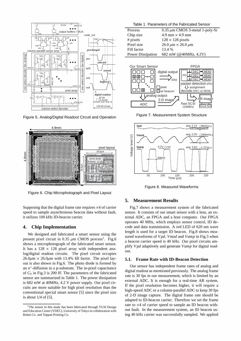
5. Measurement ResultsFig.7 shows a measurement system of the fabricated
sensor. It consists of our smart sensor with a lens, an ex-ternal ADC, an FPGA and a host computer. Our FPGAoperates 40 MHz, which employs sensor control, ID de-code and data transmission. A red LED of 620 nm wavelength is used for a target ID beacon. Fig.8 shows mea-sured waveforms of V pd, Vmod and Vamp in Fig.3 whena beacon carrier speed is 40 kHz. Our pixel circuits am-plify V pd adaptively and generate Vamp for digital read-out.
5.1. Frame Rate with ID-Beacon Detection
Our sensor has independent frame rates of analog anddigital readout as mentioned previously. The analog framerate is 30 fps in our measurement, which is limited by anexternal ADC. It is enough for a real-time AR system.If the pixel resolution becomes higher, it will require ahigh-speed ADC or a column-parallel ADC to keep 30 fpsof 2-D image capture. The digital frame rate should beadapted to ID-beacon carrier. Therefore we set the framerate to ×4 of carrier speed to sample an ID beacon with-out fault. In the measurement system, an ID beacon us-ing 40 kHz carrier was successfully sampled. We applied

Table 2. Performance Comparison
# pixels pixel size carrier data bandwidth AR images/sA Standard CCD Imager [3] N/A N/A 15 Hz 6 bit/ID·sec 0.2 fpsYoshimura, ISSCC’01 [4, 5] 192 × 124 †46.4 × 54.0 µm2 4 kHz 120 bit/ID·sec 15 fpsOur Present Smart Imager 128 × 128 †26.0 × 26.0 µm2 40 kHz 4850 bit/ID·sec 30 fps
†Both of them are fabricated in 0.35 µm process
Captured 2-D ImageCaptured 2-D Image
Acquired Location of BeaconAcquired Location of Beacon
ID and Additional Info.ID and Additional Info.from ID beacon
Camera ModuleCamera Module[1032: StarWars R2-D2][1032: StarWars R2-D2]
Figure 9. Reproduced Image with ID Information
packet transmission to our measurement system for asyn-chronous ID-beacon sampling. A packet consists of 4-bitheader, 16-bit coded data and 2-bit footer to transfer 8-bitdata for ID. In addition, a packet sequence of ID beacon isrepeated 3 times in one frame of AR images. This packetprotocol is based on [4]. In this situation, the data band-width is 4850 bit/ID·sec, which provides 160-bit data foreach target ID in 30 fps. Our proposed scheme has morepotential of high-speed sampling since it is limited by thesensor control speed by an FPGA and the photo sensitivityof a standard digital CMOS process. Fig.9 shows a repro-duced image with ID information from a blinking LED. Ithas additional information of the target object as well asits ID number due to large capacity of bandwidth.
5.2. Sensitivity and Dynamic RangeFig.10 shows the sensitivity and dynamic range of ID-
beacon detection. Our pixel circuit can detect a feeble in-cident swing of ID beacon in wide range of background il-lumination. The minimum detectable intensity of ID bea-con is measured using TEGs of a pixel circuit. To eval-uate the sensitivity of the photo detection, the ID-beaconintensity and the background intensity are normalized bythe photo current Ipd of each incident light. The illumi-nance corresponding to the background photo current isshown in Fig.10 (in the upper axis) for reference. Wedefine 10 log Esig/Ebg as SBR (Signal-to-Background Ra-tio), which stands for the sensitivity of beacon detection.High sensitivity below -10.0 dB SBR is achieved in widerange of > 40 dB background illumination.
5.3. Performance ComparisonThe performance comparison is summarized in Table 2.
The AR system using a 30-fps CCD imager provides 0.2AR images/sec with 16 IDs/frame [3]. Even the state-of-the-art high-speed CMOS imager [6], which achieves 10kfps imaging, utilizes only 2.5 kHz beacon carrier. The ARsystem [4] using a special image sensor [5] allows 4 kHzbeacon carrier. It, however, has the capability to recognizeonly 8-bit IDs/frame in 15 fps. Our present smart sensor
1
10
10
10
1 2
2
2
3
3
3
4
4 5 6
510 10 10 10 10
0dB SBR0dB SBR
-15.4dB SBR (min.)
measurement results
-10dB SBR-10dB SBR -20dB SBR-20dB SBR
> 40dB DR (< -10dB SBR)> 40dB DR (< -10dB SBR)
Background light intensity Ebg (a.u.)
10 10 10 10 10Background illuminance (lx)
Det
ecta
ble
ID b
eaco
n in
tens
ity E
sig
(a.u
.)
DetectableDetectable
Non-Detectable
Figure 10. Sensitivity and Dynamic Range of ID-Beacon Detection
utilizes 40 kHz carrier and recognizes 160-bit IDs/framein 30 fps in the same situation. The large capacity of band-width has a potential to attach additional and meaningfulinformation to an AR image from the target objects.
6. ConclusionsOur 128 × 128 smart sensor achieves 30-fps scene cap-
ture, 4850 bit/ID·sec using 40 kHz carrier, and < -10.0 dBsignal-to-background ratio (SBR) in > 40 dB backgroundillumination for a high-speed and robust AR system withactive optical devices. It enables to get a scene image, lo-cations, IDs and additional information of multiple targetobjects simultaneously in real time. The advanced perfor-mance provides the next step for a practical AR system.
7. References[1] J. Rekimoto et al., “CyberCode: Designing Augmented Re-
ality Environments with Visual Tags,” ACM Designing Aug-mented Reality Environments (DARE 2000), pp.1–10, 2000.
[2] Roy Want et al., “Bridging Physical and Virtual Worlds withElectronic Tags,” ACM Conference on Human Factors inComputing Systems (CHI’99), pp. 370–377, 1999.
[3] D. J. Moore et al., “Implementing Phicons: CombiningComputer Vision with InfraRed Technology for InteractivePhysical Icons.,” ACM Symposium on User Interface Soft-ware and Technology (UIST’99), pp.67–68, 1999.
[4] N. Matsushita et al., “ID Cam: A Smart Camera for SceneCapturing and ID Recognition,” IPSJ Journal, Vol. 43, No.12, pp.3664–3674, Dec. 2002.
[5] S. Yoshimura et al., “A 48kframe/s CMOS Image Sensor forReal-time 3-D Sensing and Motin Detection,” IEEE ISSCCDig. of Tech. Papers, pp.94–95, 2001.
[6] S. Kleinfelder et al., “A 10k frame/s 0.18µm CMOS DigitalPixel Sensor with Pixel-Level Memory,” IEEE ISSCC Dig.of Tech. Papers, pp.88–89, 2001.