Embed Size (px)
Citation preview
REV. B
Information furnished by Analog Devices is believed to be accurate andreliable. However, no responsibility is assumed by Analog Devices for itsuse, nor for any infringements of patents or other rights of third partieswhich may result from its use. No license is granted by implication orotherwise under any patent or patent rights of Analog Devices.
aAD603*
FEATURES
“Linear in dB” Gain Control
Pin Programmable Gain Ranges
–11 dB to +31 dB with 90 MHz Bandwidth
+9 dB to +51 dB with 9 MHz Bandwidth
Any Intermediate Range, e.g., –1 dB to +41 dB with
30 MHz Bandwidth
Bandwidth Independent of Variable Gain
1.3 nV/√Hz Input Noise Spectral Density
60.5 dB Typical Gain Accuracy
MIL-STD-883 Compliant and DESC Versions Available
APPLICATIONS
RF/IF AGC Amplifier
Video Gain Control
A/D Range Extension
Signal Measurement
© Analog Devices, Inc., 1995
One Technology Way, P.O. Box 9106, Norwood. MA 02062-9106, U.S.A.
Tel: 617/329-4700 Fax: 617/326-8703
Low Noise, 90 MHzVariable-Gain Amplifier
PRODUCT DESCRIPTIONThe AD603 is a low noise, voltage-controlled amplifier for usein RF and IF AGC systems. It provides accurate, pin selectablegains of –11 dB to +31 dB with a bandwidth of 90 MHz or+9 dB to +51 dB with a bandwidth of 9 MHz. Any intermediategain range may be arranged using one external resistor. Theinput referred noise spectral density is only 1.3 nV/√Hz andpower consumption is 125 mW at the recommended ±5 Vsupplies.
The decibel gain is “linear in dB,” accurately calibrated, andstable over temperature and supply. The gain is controlled at a
*Patented.X-AMP is a trademark of Analog Devices, Inc.
FUNCTIONAL BLOCK DIAGRAM
GAIN
CONTROLINTERFACE
6.44kΩ
PRECISION PASSIVE
INPUT ATTENUATOR
FIXED GAIN
AMPLIFIER
VOUT
FDBK
GPOS
GNEG
SCALINGREFERENCE
0dB –6.02dB –12.04dB –18.06dB –24.08dB –30.1dB –36.12dB –42.14dB
R - 2R LADDER NETWORK
VINP
COMM
VG
R
4
2R
R
2R 2R
R R
2R 2R
R R
2R
R
R
3
1
2
VPOS
VNEG
8
6
5
7
694Ω*
20Ω*
*NOMINAL VALUES
AD603
high impedance (50 MΩ), low bias (200 nA) differential input;the scaling is 25 mV/dB, requiring a gain-control voltage of only1 V to span the central 40 dB of the gain range. An over- andunder-range of 1 dB is provided whatever the selected range.The gain-control response time is less than 1 µs for a 40 dBchange.
The differential gain-control interface allows the use of eitherdifferential or single-ended positive or negative control voltages.Several of these amplifiers may be cascaded and their gain-con-trol gains offset to optimize the system S/N ratio.
The AD603 can drive a load impedance as low as 100 Ω withlow distortion. For a 500 Ω load in shunt with 5 pF, the totalharmonic distortion for a ±1 V sinusoidal output at 10 MHz istypically –60 dBc. The peak specified output is ±2.5 V mini-mum into a 500 Ω load, or ±1 V into a 100 Ω load.
The AD603 uses a proprietary circuit topology—the X-AMP™.The X-AMP comprises a variable attenuator of 0 dB to –42.14 dB followed by a fixed-gain amplifier. Because of theattenuator, the amplifier never has to cope with large inputs andcan use negative feedback to define its (fixed) gain and dynamicperformance. The attenuator has an input resistance of 100 Ω,laser trimmed to ±3%, and comprises a seven-stage R-2R laddernetwork, resulting in an attenuation between tap points of6.021 dB. A proprietary interpolation technique provides a con-tinuous gain-control function which is linear in dB.
The AD603A is specified for operation from –40°C to +85°Cand is available in both 8-pin SOIC (R) and 8-pin ceramic DIP(Q). The AD603S is specified for operation from –55°C to+125°C and is available in an 8-pin ceramic DIP (Q). TheAD603 is also available under DESC SMD 5962-94572.
AD603–SPECIFICATIONS
REV. B–2–
Model AD603Parameter Conditions Min Typ Max Units
INPUT CHARACTERISTICSInput Resistance Pins 3 to 4 97 100 103 ΩInput Capacitance 2 pFInput Noise Spectral Density1 Input Short Circuited 1.3 nV/√HzNoise Figure f = 10 MHz, Gain = max, RS = 10 Ω 8.8 dB1 dB Compression Point f = 10 MHz, Gain = max, RS = 10 Ω –11 dBmPeak Input Voltage ±1.4 ±2 V
OUTPUT CHARACTERISTICS–3 dB Bandwidth VOUT = 100 mV rms 90 MHzSlew Rate RL ≥ 500 Ω 275 V/µsPeak Output2 RL ≥ 500 Ω ±2.5 ±3.0 VOutput Impedance f ≤ 10 MHz 2 ΩOutput Short-Circuit Current 50 mAGroup Delay Change vs. Gain f = 3 MHz; Full Gain Range ±2 nsGroup Delay Change vs. Frequency VG = 0 V; f = 1 MHz to 10 MHz ±2 nsDifferential Gain 0.2 %Differential Phase 0.2 DegreeTotal Harmonic Distortion f = 10 MHz, VOUT = 1 V rms –60 dBc3rd Order Intercept f = 40 MHz, Gain = max, RS = 50 Ω 15 dBm
ACCURACYGain Accuracy –500 mV ≤ VG ≤ +500 mV ±0.5 ±1 dB
TMIN to TMAX ±1.5Output Offset Voltage3 VG = 0 V 20 mV
TMIN to TMAX 30Output Offset Variation vs. VG –500 mV ≤ VG ≤ +500 mV 20 mV
TMIN to TMAX 30 mV
GAIN CONTROL INTERFACEGain Scaling Factor 39.4 40 40.6 dB/V
TMIN to TMAX 38 42 dB/VCommon-Mode Range –1.2 +2.0 VInput Bias Current 200 nAInput Offset Current 10 nADifferential Input Resistance Pins 1 to 2 50 MΩResponse Rate Full 40 dB Gain Change 40 dB/µs
POWER SUPPLYSpecified Operating Range ±4.75 ±5.25 VQuiescent Current 12.5 17 mA
TMIN to TMAX 20 mA
NOTES1Typical open or short-circuited input; noise is lower when system is set to maximum gain and input is short-circuited. This figure includes the effects of both voltageand current noise sources.
2Using resistive loads of 500 Ω or greater, or with the addition of a 1 kΩ pull-down resistor when driving lower loads.3The dc gain of the main amplifier in the AD603 is ×35.7; thus, an input offset of 100 µV becomes a 3.57 mV output offset.
Specifications shown in boldface are tested on all production units at final electrical test. Results from those tests are used to calculate outgoing quality levels. All minand max specifications are guaranteed, although only those shown in boldface are tested on all production units.
Specifications subject to change without notice.
(@ TA = + 25°C, VS = ±5 V, –500 mV ≤ VG ≤ +500 mV, –10 dB to +30 dB Gain Range,RL = 500 Ω, and CL = 5 pF, unless otherwise noted.)
AD603
REV. B –3–
ABSOLUTE MAXIMUM RATINGS1
Supply Voltage ±VS . . . . . . . . . . . . . . . . . . . . . . . . . . . . ±7.5 VInternal Voltage VINP (Pin 3) . . . . . . . . . . . ±2 V Continuous
. . . . . . . . . . . . . . . . . . . . . . . . . . . . . . . . . . . . ±VS for 10 msGNEG, GPOS (Pins 1, 2) . . . . . . . . . . . . . . . . . . . . . . . ±VS
Internal Power Dissipation2 . . . . . . . . . . . . . . . . . . . . 400 mWOperating Temperature Range
AD603A . . . . . . . . . . . . . . . . . . . . . . . . . . . –40°C to +85°CAD603S . . . . . . . . . . . . . . . . . . . . . . . . . . –55°C to +125°C
Storage Temperature Range . . . . . . . . . . . . –65°C to +150°CLead Temperature Range (Soldering 60 sec) . . . . . . . . +300°CNOTES1Stresses above those listed under “Absolute Maximum Ratings” may causepermanent damage to the device. This is a stress rating only and functionaloperation of the device at these or any other conditions above those indicated in theoperational section of this specification is not implied. Exposure to absolutemaximum rating conditions for extended periods may affect device reliability.
2Thermal Characteristics:8-Pin SOIC Package: θJA = 155°C/Watt, θJC = 33°C/Watt8-Pin Ceramic Package: θJA = 140°C/Watt, θJC = 15°C/Watt
ORDERING GUIDE
Temperature Package PackagePart Number Range Description1 Option1
AD603AR –40°C to +85°C 8-Pin SOIC R-8AD603AQ –40°C to +85°C 8-Pin Ceramic DIP Q-8AD603SQ/883B2 –55°C to +125°C 8-Pin Ceramic DIP Q-8
NOTES1R = SOIC; Q = Cerdip.2Refer to AD603 Military data sheet. Also available as 5962-9457203MPA.
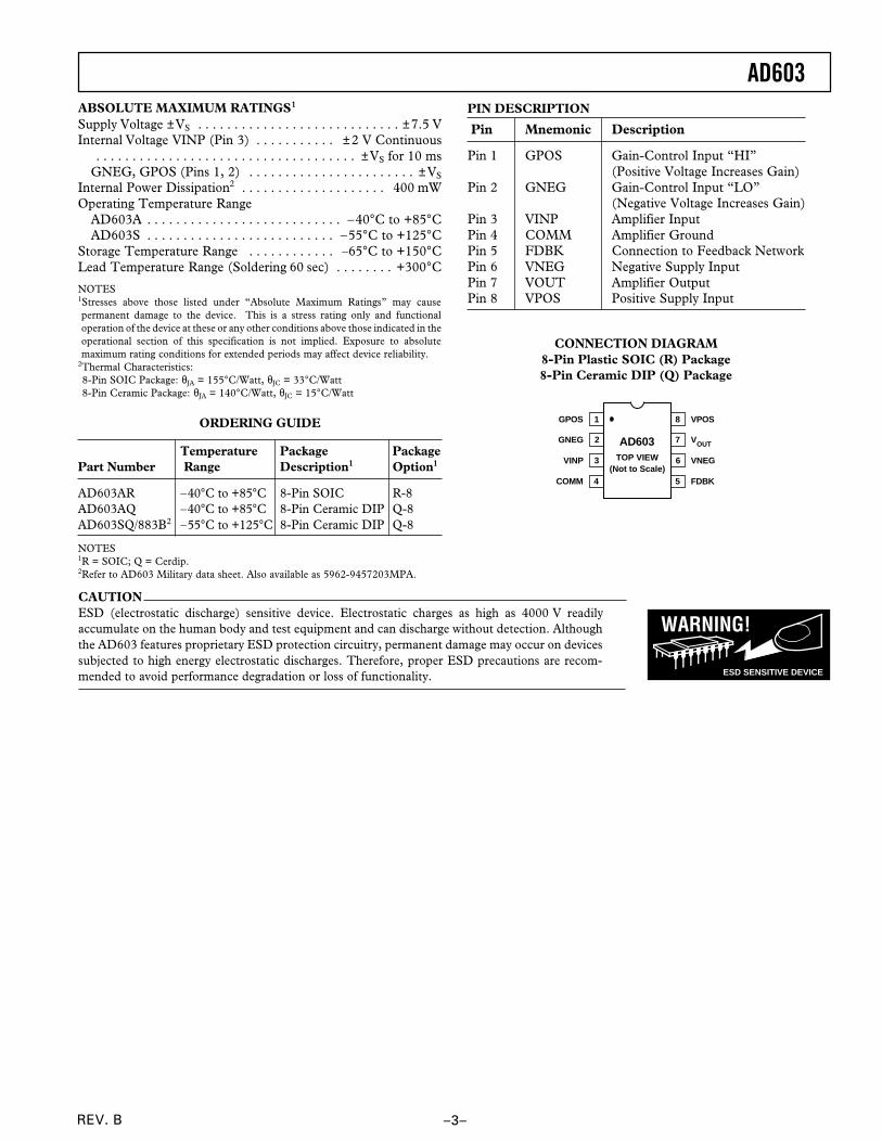
PIN DESCRIPTION
Pin Mnemonic Description
Pin 1 GPOS Gain-Control Input “HI”(Positive Voltage Increases Gain)
Pin 2 GNEG Gain-Control Input “LO”(Negative Voltage Increases Gain)
Pin 3 VINP Amplifier InputPin 4 COMM Amplifier GroundPin 5 FDBK Connection to Feedback NetworkPin 6 VNEG Negative Supply InputPin 7 VOUT Amplifier OutputPin 8 VPOS Positive Supply Input
CONNECTION DIAGRAM8-Pin Plastic SOIC (R) Package8-Pin Ceramic DIP (Q) Package
GPOS
GNEG
VINP
COMM
VPOS
VOUT
VNEG
FDBK
1
2
3
4
8
7
6
5
TOP VIEW(Not to Scale)
AD603
WARNING!
ESD SENSITIVE DEVICE
CAUTIONESD (electrostatic discharge) sensitive device. Electrostatic charges as high as 4000 V readilyaccumulate on the human body and test equipment and can discharge without detection. Althoughthe AD603 features proprietary ESD protection circuitry, permanent damage may occur on devicessubjected to high energy electrostatic discharges. Therefore, proper ESD precautions are recom-mended to avoid performance degradation or loss of functionality.
REV. B–4–
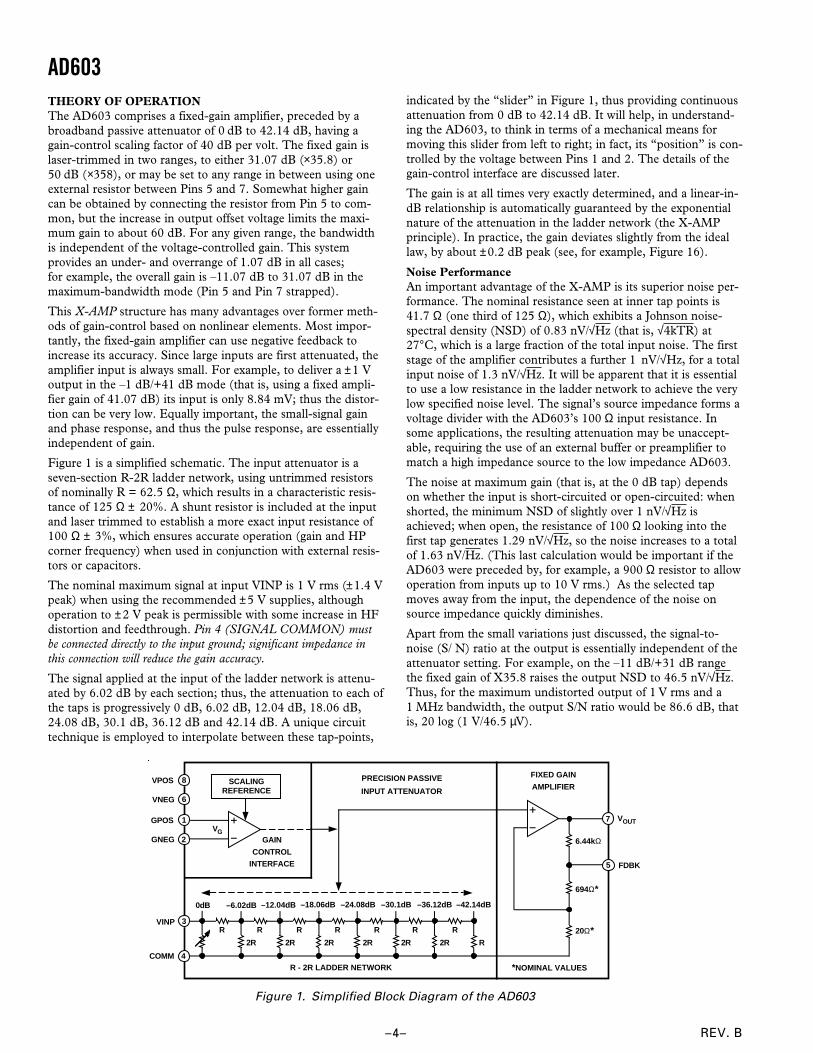
AD603THEORY OF OPERATIONThe AD603 comprises a fixed-gain amplifier, preceded by abroadband passive attenuator of 0 dB to 42.14 dB, having again-control scaling factor of 40 dB per volt. The fixed gain islaser-trimmed in two ranges, to either 31.07 dB (×35.8) or50 dB (×358), or may be set to any range in between using oneexternal resistor between Pins 5 and 7. Somewhat higher gaincan be obtained by connecting the resistor from Pin 5 to com-mon, but the increase in output offset voltage limits the maxi-mum gain to about 60 dB. For any given range, the bandwidthis independent of the voltage-controlled gain. This systemprovides an under- and overrange of 1.07 dB in all cases;for example, the overall gain is –11.07 dB to 31.07 dB in themaximum-bandwidth mode (Pin 5 and Pin 7 strapped).
This X-AMP structure has many advantages over former meth-ods of gain-control based on nonlinear elements. Most impor-tantly, the fixed-gain amplifier can use negative feedback toincrease its accuracy. Since large inputs are first attenuated, theamplifier input is always small. For example, to deliver a ±1 Voutput in the –1 dB/+41 dB mode (that is, using a fixed ampli-fier gain of 41.07 dB) its input is only 8.84 mV; thus the distor-tion can be very low. Equally important, the small-signal gainand phase response, and thus the pulse response, are essentiallyindependent of gain.
Figure 1 is a simplified schematic. The input attenuator is aseven-section R-2R ladder network, using untrimmed resistorsof nominally R = 62.5 Ω, which results in a characteristic resis-tance of 125 Ω ± 20%. A shunt resistor is included at the inputand laser trimmed to establish a more exact input resistance of100 Ω ± 3%, which ensures accurate operation (gain and HPcorner frequency) when used in conjunction with external resis-tors or capacitors.
The nominal maximum signal at input VINP is 1 V rms (±1.4 Vpeak) when using the recommended ±5 V supplies, althoughoperation to ±2 V peak is permissible with some increase in HFdistortion and feedthrough. Pin 4 (SIGNAL COMMON) mustbe connected directly to the input ground; significant impedance inthis connection will reduce the gain accuracy.
The signal applied at the input of the ladder network is attenu-ated by 6.02 dB by each section; thus, the attenuation to each ofthe taps is progressively 0 dB, 6.02 dB, 12.04 dB, 18.06 dB,24.08 dB, 30.1 dB, 36.12 dB and 42.14 dB. A unique circuittechnique is employed to interpolate between these tap-points,
indicated by the “slider” in Figure 1, thus providing continuousattenuation from 0 dB to 42.14 dB. It will help, in understand-ing the AD603, to think in terms of a mechanical means formoving this slider from left to right; in fact, its “position” is con-trolled by the voltage between Pins 1 and 2. The details of thegain-control interface are discussed later.
The gain is at all times very exactly determined, and a linear-in-dB relationship is automatically guaranteed by the exponentialnature of the attenuation in the ladder network (the X-AMPprinciple). In practice, the gain deviates slightly from the ideallaw, by about ±0.2 dB peak (see, for example, Figure 16).
Noise PerformanceAn important advantage of the X-AMP is its superior noise per-formance. The nominal resistance seen at inner tap points is41.7 Ω (one third of 125 Ω), which exhibits a Johnson noise-spectral density (NSD) of 0.83 nV/√Hz (that is, √4kTR) at27°C, which is a large fraction of the total input noise. The firststage of the amplifier contributes a further 1 nV/√Hz, for a totalinput noise of 1.3 nV/√Hz. It will be apparent that it is essentialto use a low resistance in the ladder network to achieve the verylow specified noise level. The signal’s source impedance forms avoltage divider with the AD603’s 100 Ω input resistance. Insome applications, the resulting attenuation may be unaccept-able, requiring the use of an external buffer or preamplifier tomatch a high impedance source to the low impedance AD603.
The noise at maximum gain (that is, at the 0 dB tap) dependson whether the input is short-circuited or open-circuited: whenshorted, the minimum NSD of slightly over 1 nV/√Hz isachieved; when open, the resistance of 100 Ω looking into thefirst tap generates 1.29 nV/√Hz, so the noise increases to a totalof 1.63 nV/Hz. (This last calculation would be important if theAD603 were preceded by, for example, a 900 Ω resistor to allowoperation from inputs up to 10 V rms.) As the selected tapmoves away from the input, the dependence of the noise onsource impedance quickly diminishes.
Apart from the small variations just discussed, the signal-to-noise (S/ N) ratio at the output is essentially independent of theattenuator setting. For example, on the –11 dB/+31 dB rangethe fixed gain of X35.8 raises the output NSD to 46.5 nV/√Hz.Thus, for the maximum undistorted output of 1 V rms and a1 MHz bandwidth, the output S/N ratio would be 86.6 dB, thatis, 20 log (1 V/46.5 µV).
GAIN
CONTROLINTERFACE
6.44kΩ
PRECISION PASSIVE
INPUT ATTENUATOR
FIXED GAIN
AMPLIFIER
VOUT
FDBK
GPOS
GNEG
SCALINGREFERENCE
0dB –6.02dB –12.04dB –18.06dB –24.08dB –30.1dB –36.12dB –42.14dB
R - 2R LADDER NETWORK
VINP
COMM
VG
R
4
2R
R
2R 2R
R R
2R 2R
R R
2R
R
R
3
1
2
VPOS
VNEG
8
6
5
7
694Ω*
20Ω*
*NOMINAL VALUES
Figure 1. Simplified Block Diagram of the AD603
AD603
REV. B –5–
The Gain-Control InterfaceThe attenuation is controlled through a differential, high-impedance (50 MΩ) input, with a scaling factor which is laser-trimmed to 40 dB per volt, that is, 25 mV/dB. An internalbandgap reference ensures stability of the scaling with respect tosupply and temperature variations.
When the differential input voltage VG = 0 V, the attenuator“slider” is centered, providing an attenuation of 21.07 dB. Forthe maximum bandwidth range, this results in an overall gain of10 dB (= –21.07 dB + 31.07 dB). When the control input is–500 mV, the gain is lowered by 20 dB (= 0.500 V × 40 dB/V),to –10 dB; when set to +500 mV, the gain is increased by20 dB, to 30 dB. When this interface is overdriven in eitherdirection, the gain approaches either –11.07 dB (= –42.14 dB +31.07 dB) or 31.07 dB (= 0 + 31.07 dB), respectively. The onlyconstraint on the gain-control voltage is that it be kept withinthe common-mode range (–1.2 V to +2.0 V assuming +5 V sup-plies) of the gain control interface.
The basic gain of the AD603 can thus be calculated using thefollowing simple expression:
Gain (dB) = 40 VG + 10 Eq. (1)
where VG is in volts. When Pins 5 and 7 are strapped (see nextsection) the gain becomes
Gain (dB) = 40 VG + 20 for 0 to +40 dB
and
Gain (dB) = 40 VG + 30 for +10 to +50 dB Eq. (2)
The high impedance gain-control input ensures minimal loadingwhen driving many amplifiers in multiple channel or cascadedapplications. The differential capability provides flexibility inchoosing the appropriate signal levels and polarities for variouscontrol schemes.
For example, if the gain is to be controlled by a DAC providinga positive only ground-referenced output, the “Gain ControlLO” (GNEG) pin should be biased to a fixed offset of+500 mV, to set the gain to –10 dB when “Gain Control HI”(GPOS) is at zero, and to 30 dB when at +1.00 V.
It is a simple matter to include a voltage divider to achieve otherscaling factors. When using an 8-bit DAC having an FS outputof +2.55 V (10 mV/bit), a divider ratio of 2 (generating 5 mV/bit) would result in a gain-setting resolution of 0.2 dB/bit. Theuse of such offsets is valuable when two AD603s are cascaded,when various options exist for optimizing the S/N profile, as willbe shown later.
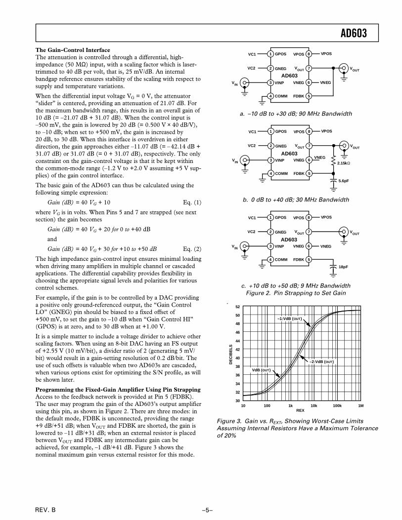
Programming the Fixed-Gain Amplifier Using Pin StrappingAccess to the feedback network is provided at Pin 5 (FDBK).The user may program the gain of the AD603’s output amplifierusing this pin, as shown in Figure 2. There are three modes: inthe default mode, FDBK is unconnected, providing the range+9 dB/+51 dB; when VOUT and FDBK are shorted, the gain islowered to –11 dB/+31 dB; when an external resistor is placedbetween VOUT and FDBK any intermediate gain can beachieved, for example, –1 dB/+41 dB. Figure 3 shows thenominal maximum gain versus external resistor for this mode.
VC1
VC2
VNEGVNEG
FDBK
VPOS
COMM
VINP
GNEG
AD603
GPOS
VIN
VPOS
VOUT
8
7
3
5
1
2
6
4
VOUT
a. –10 dB to +30 dB; 90 MHz Bandwidth
VC1
VC2
VNEGVNEG
FDBK
VPOS
COMM
VINP
GNEG
AD603
GPOS
VIN
VPOS
VOUT
8
7
3
5
1
2
6
4
VOUT
2.15kΩ
5.6pF
b. 0 dB to +40 dB; 30 MHz Bandwidth
VC1
VC2
VNEGVNEG
FDBK
VPOS
COMM
VINP
GNEG
AD603
GPOS
VIN
VPOS
VOUT
8
7
3
5
1
2
6
4
VOUT
18pF
c. +10 dB to +50 dB; 9 MHz Bandwidth
Figure 2. Pin Strapping to Set Gain
52
50
3010 100 1M100k10k1k
48
46
44
42
40
38
36
34
32
REX
DE
CIB
EL
S
–1:VdB (OUT)
VdB (OUT)
–2:VdB (OUT)
Figure 3. Gain vs. REXT, Showing Worst-Case Limits
Assuming Internal Resistors Have a Maximum Tolerance
of 20%
REV. B–6–
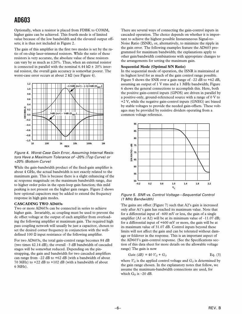
AD603Optionally, when a resistor is placed from FDBK to COMM,higher gains can be achieved. This fourth mode is of limitedvalue because of the low bandwidth and the elevated output off-sets; it is thus not included in Figure 2.
The gain of this amplifier in the first two modes is set by the ra-tio of on-chip laser-trimmed resistors. While the ratio of theseresistors is very accurate, the absolute value of these resistorscan vary by as much as ±20%. Thus, when an external resistoris connected in parallel with the nominal 6.44 kΩ ± 20% inter-nal resistor, the overall gain accuracy is somewhat poorer. Theworst-case error occurs at about 2 kΩ (see Figure 4).
1.2
1.0
–1.010 100 1M100k10k1k
0.8
0.6
0.4
0.2
0.0
–0.2
–0.4
–0.6
–0.8
REX
DE
CIB
EL
S
–1:VdB (OUT) – (–1):VdB (OREF )
VdB (OUT) – VdB (OREF)
Figure 4. Worst-Case Gain Error, Assuming Internal Resis-
tors Have a Maximum Tolerance of –20% (Top Curve) or
+20% (Bottom Curve)
While the gain-bandwidth product of the fixed-gain amplifier isabout 4 GHz, the actual bandwidth is not exactly related to themaximum gain. This is because there is a slight enhancing of theac response magnitude on the maximum bandwidth range, dueto higher order poles in the open-loop gain function; this mildpeaking is not present on the higher gain ranges. Figure 2 showshow optional capacitors may be added to extend the frequencyresponse in high gain modes.
CASCADING TWO AD603sTwo or more AD603s can be connected in series to achievehigher gain. Invariably, ac coupling must be used to prevent thedc offset voltage at the output of each amplifier from overload-ing the following amplifier at maximum gain. The required highpass coupling network will usually be just a capacitor, chosen toset the desired corner frequency in conjunction with the well-defined 100 Ω input resistance of the following amplifier.
For two AD603s, the total gain-control range becomes 84 dB(two times 42.14 dB); the overall –3 dB bandwidth of cascadedstages will be somewhat reduced. Depending on the pin-strapping, the gain and bandwidth for two cascaded amplifierscan range from –22 dB to +62 dB (with a bandwidth of about70 MHz) to +22 dB to +102 dB (with a bandwidth of about6 MHz).
There are several ways of connecting the gain-control inputs incascaded operation. The choice depends on whether it is impor-tant to achieve the highest possible Instantaneous Signal-to-Noise Ratio (ISNR), or, alternatively, to minimize the ripple inthe gain error. The following examples feature the AD603 pro-grammed for maximum bandwidth; the explanations apply toother gain/bandwidth combinations with appropriate changes tothe arrangements for setting the maximum gain.
Sequential Mode (Optimal S/N Ratio)In the sequential mode of operation, the ISNR is maintained atits highest level for as much of the gain control range possible.Figure 5 shows the SNR over a gain range of –22 dB to +62 dB,assuming an output of 1 V rms and a 1 MHz bandwidth; Figure6 shows the general connections to accomplish this. Here, boththe positive gain-control inputs (GPOS) are driven in parallel bya positive-only, ground-referenced source with a range of 0 V to+2 V, while the negative gain-control inputs (GNEG) arc biasedby stable voltages to provide the needed gain-offsets. These volt-ages may be provided by resistive dividers operating from acommon voltage reference.
90
502.2
60
55
0.2–0.2
70
65
75
80
85
1.81.41.00.6
VC
S/N
RA
TIO
– d
B
Figure 5. SNR vs. Control Voltage—Sequential Control
(1 MHz Bandwidth)
The gains are offset (Figure 7) such that A2’s gain is increasedonly after A1’s gain has reached its maximum value. Note thatfor a differential input of –600 mV or less, the gain of a singleamplifier (A1 or A2) will be at its minimum value of –11.07 dB;for a differential input of +600 mV or more, the gain will be atits maximum value of 31.07 dB. Control inputs beyond theselimits will not affect the gain and can be tolerated without dam-age or foldover in the response. This is an important aspect ofthe AD603’s gain-control response. (See the Specifications sec-tion of this data sheet for more details on the allowable voltagerange) The gain is now
Gain (dB) = 40 VG + GO Eq. (3)
where VG is the applied control voltage and GO is determined bythe gain range chosen. In the explanatory notes that follow, weassume the maximum-bandwidth connections are used, forwhich GO is –20 dB.
AD603
REV. B –7–
GPOS GNEG
INPUT0dB GPOS GNEG 31.07dB
–42.14dB31.07dB
0dB –11.07dB
OUTPUT20dB
GPOS GNEG31.07dB
0dBINPUT0dB 31.07dB
31.07dB
0dB 28.93dB
OUTPUT60dB
VC = 2.5V
GPOS GNEG31.07dB
–40.00dBINPUT0dB GPOS GNEG
–42.14dB–8.93dB
–40.00dB –51.07dB
OUTPUT–20dB
A1 A2
(a)
(b)
(c)
0dB
VG1
31.07dB
VO2 = 1.526V
VG1
VG1 VO2 = 1.526V
VG2
VG2
GPOS GNEG
–2.14dB
VG2 VO2 = 1.526V
VO1 = 0.473V
VO1 = 0.473V
VO1 = 0.473VVC = 1.25V
VC = 0V
31.07dB
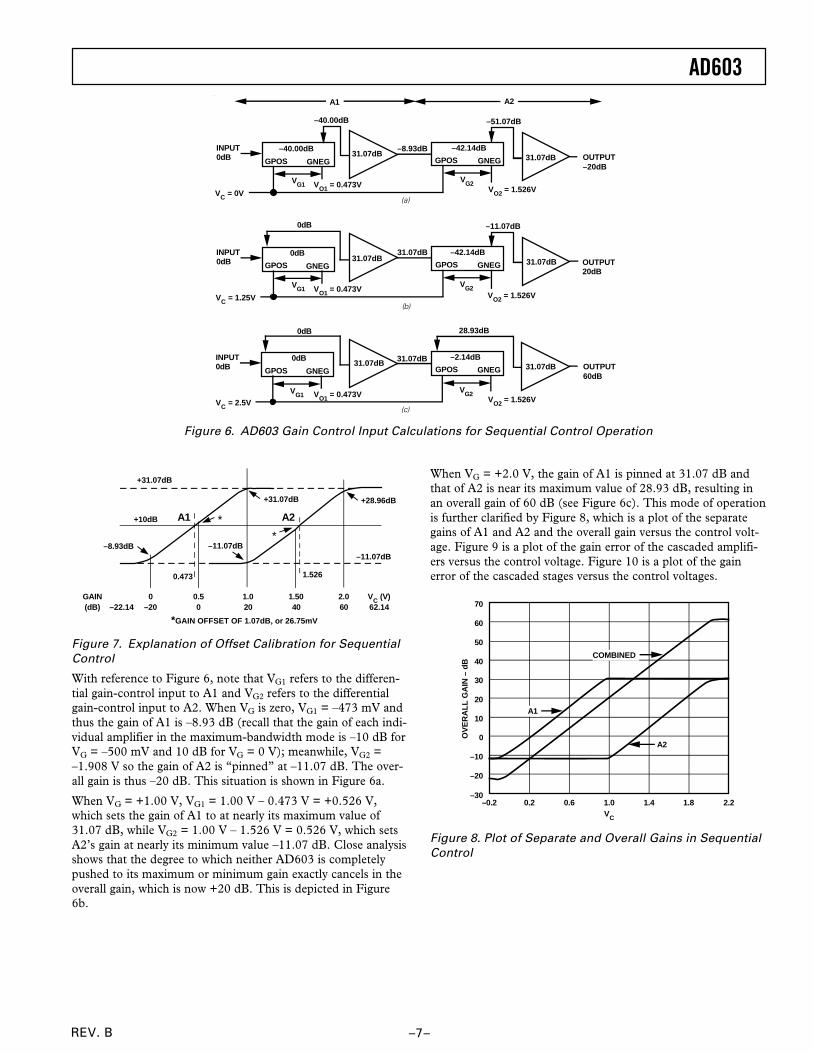
Figure 6. AD603 Gain Control Input Calculations for Sequential Control Operation
**
0.473 1.526
1.5040
2.060
0.50
1.020
0–20
VC (V)62.14–22.14
GAIN(dB)
–8.93dB
+10dB
+31.07dB
–11.07dB–11.07dB
+31.07dB +28.96dB
A2A1
*GAIN OFFSET OF 1.07dB, or 26.75mV
Figure 7. Explanation of Offset Calibration for Sequential
Control
With reference to Figure 6, note that VG1 refers to the differen-tial gain-control input to A1 and VG2 refers to the differentialgain-control input to A2. When VG is zero, VG1 = –473 mV andthus the gain of A1 is –8.93 dB (recall that the gain of each indi-vidual amplifier in the maximum-bandwidth mode is –10 dB forVG = –500 mV and 10 dB for VG = 0 V); meanwhile, VG2 =–1.908 V so the gain of A2 is “pinned” at –11.07 dB. The over-all gain is thus –20 dB. This situation is shown in Figure 6a.
When VG = +1.00 V, VG1 = 1.00 V – 0.473 V = +0.526 V,which sets the gain of A1 to at nearly its maximum value of31.07 dB, while VG2 = 1.00 V – 1.526 V = 0.526 V, which setsA2’s gain at nearly its minimum value –11.07 dB. Close analysisshows that the degree to which neither AD603 is completelypushed to its maximum or minimum gain exactly cancels in theoverall gain, which is now +20 dB. This is depicted in Figure6b.
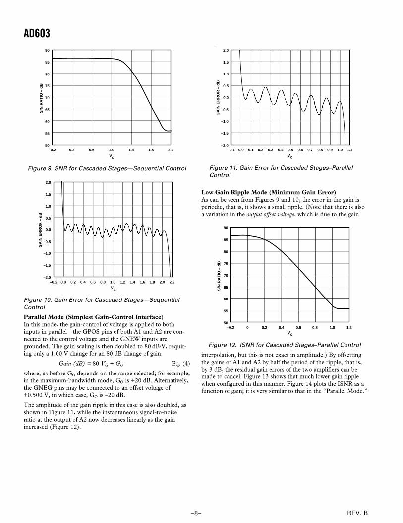
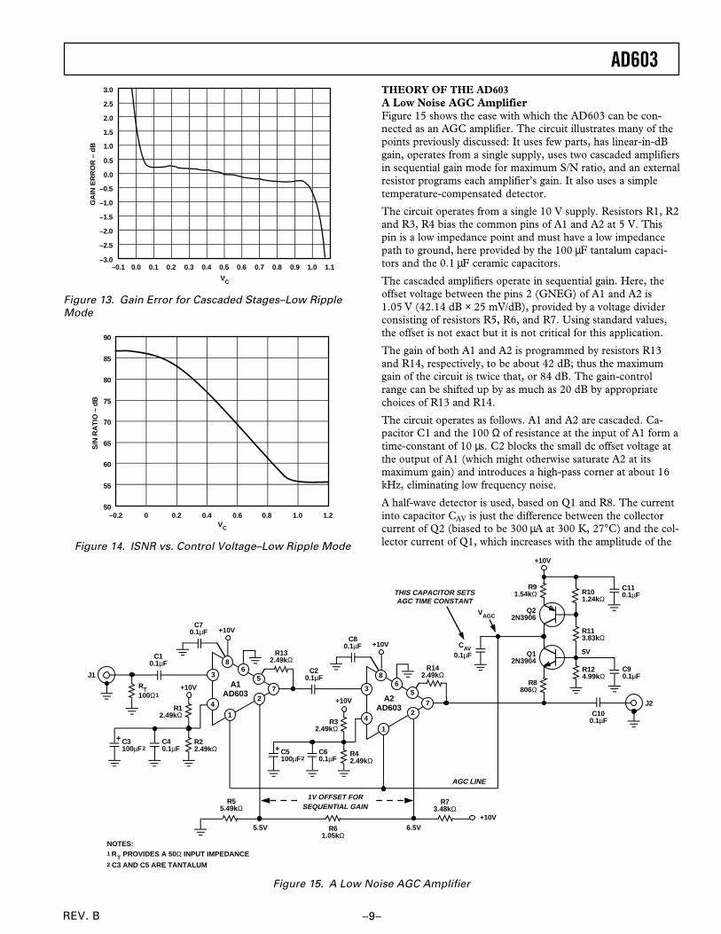
When VG = +2.0 V, the gain of A1 is pinned at 31.07 dB andthat of A2 is near its maximum value of 28.93 dB, resulting inan overall gain of 60 dB (see Figure 6c). This mode of operationis further clarified by Figure 8, which is a plot of the separategains of A1 and A2 and the overall gain versus the control volt-age. Figure 9 is a plot of the gain error of the cascaded amplifi-ers versus the control voltage. Figure 10 is a plot of the gainerror of the cascaded stages versus the control voltages.
VC
OV
ER
AL
L G
AIN
– d
B
70
–302.2
0
–20
0.2
–10
–0.2
30
10
20
40
50
60
1.81.41.00.6
A1
A2
COMBINED
Figure 8. Plot of Separate and Overall Gains in Sequential
Control
REV. B–8–
AD60390
502.2
60
55
0.2–0.2
70
65
75
80
85
1.81.41.00.6
VC
S/N
RA
TIO
– d
B
Figure 9. SNR for Cascaded Stages—Sequential Control
2.0
–2.02.2
–1.0
–1.5
0.0–0.2
0.0
–0.5
0.5
1.0
1.5
2.01.81.61.41.21.00.80.60.40.2VC
GA
IN E
RR
OR
– d
B
Figure 10. Gain Error for Cascaded Stages—Sequential
Control
Parallel Mode (Simplest Gain-Control Interface)In this mode, the gain-control of voltage is applied to bothinputs in parallel—the GPOS pins of both A1 and A2 are con-nected to the control voltage and the GNEW inputs aregrounded. The gain scaling is then doubled to 80 dB/V, requir-ing only a 1.00 V change for an 80 dB change of gain:
Gain (dB) = 80 VG + GO Eq. (4)
where, as before GO depends on the range selected; for example,in the maximum-bandwidth mode, GO is +20 dB. Alternatively,the GNEG pins may be connected to an offset voltage of+0.500 V, in which case, GO is –20 dB.
The amplitude of the gain ripple in this case is also doubled, asshown in Figure 11, while the instantaneous signal-to-noiseratio at the output of A2 now decreases linearly as the gainincreased (Figure 12).
2.0
–2.01.1
–1.0
–1.5
0.0–0.1
0.0
–0.5
0.5
1.0
1.5
1.00.90.80.70.60.50.40.30.20.1VC
GA
IN E
RR
OR
– d
B
Figure 11. Gain Error for Cascaded Stages–Parallel
Control
Low Gain Ripple Mode (Minimum Gain Error)As can be seen from Figures 9 and 10, the error in the gain isperiodic, that is, it shows a small ripple. (Note that there is alsoa variation in the output offset voltage, which is due to the gain
90
501.2
60
55
0–0.2
70
65
75
80
85
1.00.80.60.40.2VC
S/N
RA
TIO
– d
B
Figure 12. ISNR for Cascaded Stages–Parallel Control
interpolation, but this is not exact in amplitude.) By offsettingthe gains of A1 and A2 by half the period of the ripple, that is,by 3 dB, the residual gain errors of the two amplifiers can bemade to cancel. Figure 13 shows that much lower gain ripplewhen configured in this manner. Figure 14 plots the ISNR as afunction of gain; it is very similar to that in the “Parallel Mode.”
AD603
REV. B –9–
3.0
–3.01.1
–1.5
–2.5
0.0
–2.0
–0.1
0.0
–1.0
–0.5
0.5
1.0
1.5
2.5
2.0
1.00.90.80.70.60.50.40.30.20.1
VC
GA
IN E
RR
OR
– d
B
Figure 13. Gain Error for Cascaded Stages–Low Ripple
Mode
90
501.2
60
55
0–0.2
70
65
75
80
85
1.00.80.60.40.2VC
S/N
RA
TIO
– d
B
Figure 14. ISNR vs. Control Voltage–Low Ripple Mode
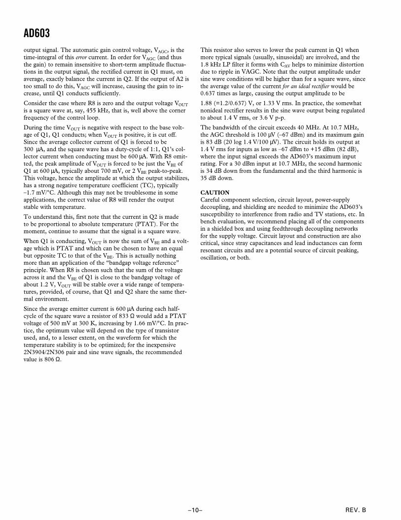
THEORY OF THE AD603A Low Noise AGC AmplifierFigure 15 shows the ease with which the AD603 can be con-nected as an AGC amplifier. The circuit illustrates many of thepoints previously discussed: It uses few parts, has linear-in-dBgain, operates from a single supply, uses two cascaded amplifiersin sequential gain mode for maximum S/N ratio, and an externalresistor programs each amplifier’s gain. It also uses a simpletemperature-compensated detector.
The circuit operates from a single 10 V supply. Resistors R1, R2and R3, R4 bias the common pins of A1 and A2 at 5 V. Thispin is a low impedance point and must have a low impedancepath to ground, here provided by the 100 µF tantalum capaci-tors and the 0.1 µF ceramic capacitors.
The cascaded amplifiers operate in sequential gain. Here, theoffset voltage between the pins 2 (GNEG) of A1 and A2 is1.05 V (42.14 dB × 25 mV/dB), provided by a voltage dividerconsisting of resistors R5, R6, and R7. Using standard values,the offset is not exact but it is not critical for this application.
The gain of both A1 and A2 is programmed by resistors R13and R14, respectively, to be about 42 dB; thus the maximumgain of the circuit is twice that, or 84 dB. The gain-controlrange can be shifted up by as much as 20 dB by appropriatechoices of R13 and R14.
The circuit operates as follows. A1 and A2 are cascaded. Ca-pacitor C1 and the 100 Ω of resistance at the input of A1 form atime-constant of 10 µs. C2 blocks the small dc offset voltage atthe output of A1 (which might otherwise saturate A2 at itsmaximum gain) and introduces a high-pass corner at about 16kHz, eliminating low frequency noise.
A half-wave detector is used, based on Q1 and R8. The currentinto capacitor CAV is just the difference between the collectorcurrent of Q2 (biased to be 300 µA at 300 K, 27°C) and the col-lector current of Q1, which increases with the amplitude of the
C20.1µF
RT100Ω1
R42.49kΩ
R32.49kΩ
C60.1µF
C5100µF2
+10V
R61.05kΩ
R55.49kΩ
R73.48kΩ
+10V6.5V5.5V
1V OFFSET FOR SEQUENTIAL GAIN
J1R8
806Ω
R91.54kΩ R10
1.24kΩ
R124.99kΩ
C90.1µF
R113.83kΩ
+10V
Q22N3906
Q12N3904
CAV0.1µF
J2
R132.49kΩ
A2AD603
C80.1µF +10V
R142.49kΩ
AGC LINE
THIS CAPACITOR SETS AGC TIME CONSTANT
VAGC
NOTES:1 RT PROVIDES A 50Ω INPUT IMPEDANCE2 C3 AND C5 ARE TANTALUM
5V
C110.1µF
8
4
1
27
6
C10.1µF
A1AD603
C70.1µF +10V
3
8
3
1
27
6
R22.49kΩ
R12.49kΩ
C40.1µF
C3100µF2
+10V
4
5
5
C100.1µF
Figure 15. A Low Noise AGC Amplifier
REV. B–10–
AD603output signal. The automatic gain control voltage, VAGC, is thetime-integral of this error current. In order for VAGC (and thusthe gain) to remain insensitive to short-term amplitude fluctua-tions in the output signal, the rectified current in Q1 must, onaverage, exactly balance the current in Q2. If the output of A2 istoo small to do this, VAGC will increase, causing the gain to in-crease, until Q1 conducts sufficiently.
Consider the case where R8 is zero and the output voltage VOUT
is a square wave at, say, 455 kHz, that is, well above the cornerfrequency of the control loop.
During the time VOUT is negative with respect to the base volt-age of Q1, Q1 conducts; when VOUT is positive, it is cut off.Since the average collector current of Q1 is forced to be300 µA, and the square wave has a duty-cycle of 1:1, Q1’s col-lector current when conducting must be 600 µA. With R8 omit-ted, the peak amplitude of VOUT is forced to be just the VBE ofQ1 at 600 µA, typically about 700 mV, or 2 VBE peak-to-peak.This voltage, hence the amplitude at which the output stabilizes,has a strong negative temperature coefficient (TC), typically–1.7 mV/°C. Although this may not be troublesome in someapplications, the correct value of R8 will render the outputstable with temperature.
To understand this, first note that the current in Q2 is madeto be proportional to absolute temperature (PTAT). For themoment, continue to assume that the signal is a square wave.
When Q1 is conducting, VOUT is now the sum of VBE and a volt-age which is PTAT and which can be chosen to have an equalbut opposite TC to that of the VBE. This is actually nothingmore than an application of the “bandgap voltage reference”principle. When R8 is chosen such that the sum of the voltageacross it and the VBE of Q1 is close to the bandgap voltage ofabout 1.2 V, VOUT will be stable over a wide range of tempera-tures, provided, of course, that Q1 and Q2 share the same ther-mal environment.
Since the average emitter current is 600 µA during each half-cycle of the square wave a resistor of 833 Ω would add a PTATvoltage of 500 mV at 300 K, increasing by 1.66 mV/°C. In prac-tice, the optimum value will depend on the type of transistorused, and, to a lesser extent, on the waveform for which thetemperature stability is to be optimized; for the inexpensive2N3904/2N306 pair and sine wave signals, the recommendedvalue is 806 Ω.
This resistor also serves to lower the peak current in Q1 whenmore typical signals (usually, sinusoidal) are involved, and the1.8 kHz LP filter it forms with CAV helps to minimize distortiondue to ripple in VAGC. Note that the output amplitude undersine wave conditions will be higher than for a square wave, sincethe average value of the current for an ideal rectifier would be0.637 times as large, causing the output amplitude to be
1.88 (=1.2/0.637) V, or 1.33 V rms. In practice, the somewhatnonideal rectifier results in the sine wave output being regulatedto about 1.4 V rms, or 3.6 V p-p.
The bandwidth of the circuit exceeds 40 MHz. At 10.7 MHz,the AGC threshold is 100 µV (–67 dBm) and its maximum gainis 83 dB (20 log 1.4 V/100 µV). The circuit holds its output at1.4 V rms for inputs as low as –67 dBm to +15 dBm (82 dB),where the input signal exceeds the AD603’s maximum inputrating. For a 30 dBm input at 10.7 MHz, the second harmonicis 34 dB down from the fundamental and the third harmonic is35 dB down.
CAUTIONCareful component selection, circuit layout, power-supplydecoupling, and shielding are needed to minimize the AD603’ssusceptibility to interference from radio and TV stations, etc. Inbench evaluation, we recommend placing all of the componentsin a shielded box and using feedthrough decoupling networksfor the supply voltage. Circuit layout and construction are alsocritical, since stray capacitances and lead inductances can formresonant circuits and are a potential source of circuit peaking,oscillation, or both.
AD603
REV. B –11–
2.50
–1.500.5
–0.50
–1.00
–0.4–0.5
0.50
0.00
1.00
1.50
2.00
0.40.30.20.10.0–0.1–0.2–0.3
GAIN VOLTAGE – Volts
GA
IN E
RR
OR
– d
B
70MHz
45MHz
10.7MHz
70MHz
455kHz
Figure 16. Gain Error vs. Gain Control
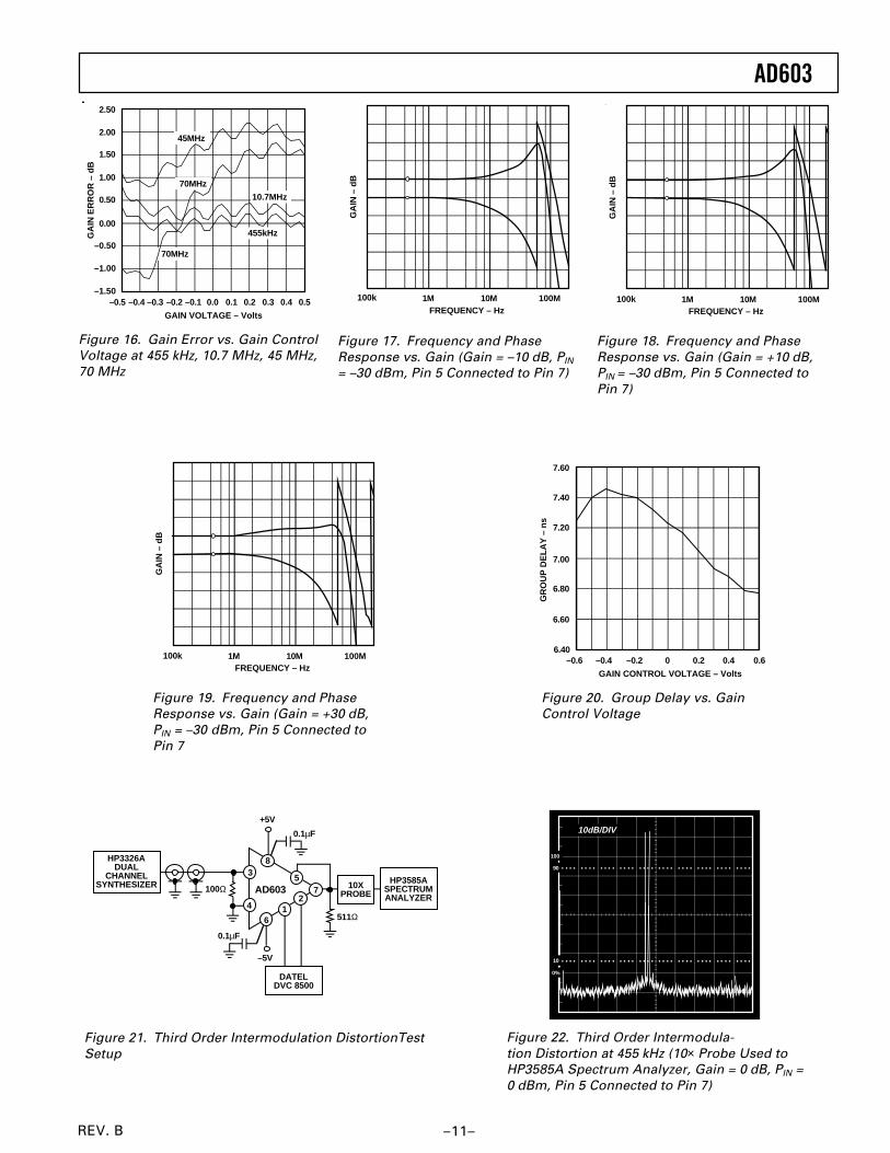
Voltage at 455 kHz, 10.7 MHz, 45 MHz,
70 MHz
FREQUENCY – Hz100k 1M 100M10M
GA
IN –
dB
Figure 17. Frequency and Phase
Response vs. Gain (Gain = –10 dB, PIN
= –30 dBm, Pin 5 Connected to Pin 7)
100k 1M 100M10MFREQUENCY – Hz
GA
IN –
dB
Figure 18. Frequency and Phase
Response vs. Gain (Gain = +10 dB,
PIN = –30 dBm, Pin 5 Connected to
Pin 7)
100k 1M 100M10MFREQUENCY – Hz
GA
IN –
dB
Figure 19. Frequency and Phase
Response vs. Gain (Gain = +30 dB,
PIN = –30 dBm, Pin 5 Connected to
Pin 7
GAIN CONTROL VOLTAGE – Volts
GR
OU
P D
EL
AY
– n
s
6.400.4–0.6 0.20–0.2–0.4
6.80
6.60
7.20
7.00
7.40
7.60
0.6
Figure 20. Group Delay vs. Gain
Control Voltage
90
100
10
0%
10dB/DIV
Figure 22. Third Order Intermodula-
tion Distortion at 455 kHz (10× Probe Used to
HP3585A Spectrum Analyzer, Gain = 0 dB, PIN =
0 dBm, Pin 5 Connected to Pin 7)
7
4
3
AD603 10X PROBE
HP3585ASPECTRUMANALYZER
+5V
0.1µF
16
–5V
0.1µF
DATELDVC 8500
HP3326ADUAL
CHANNEL SYNTHESIZER 100Ω
511Ω
2
5
8
Figure 21. Third Order Intermodulation DistortionTest
Setup
REV. B–12–
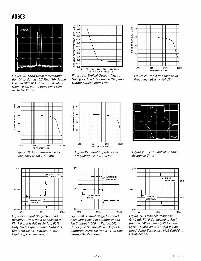
AD603
10
90
100
0%
10dB/DIV
Figure 23. Third Order Intermodula-
tion Distortion at 10.7 MHz (10× Probe
Used to HP3585A Spectrum Analyzer,
Gain = 0 dB, PIN = 0 dBm, Pin 5 Con-
nected to Pin 7)
100k 1M 100M10M
98
102
100
96
INP
UT
IMP
ED
AN
CE
– O
hm
s
FREQUENCY – Hz
Figure 26. Input Impedance vs.
Frequency (Gain = +10 dB)
4.5V
–500mV451ns–49ns
500mV
50ns
INPUT GND 1V/DIV
OUTPUT GND 500mV/DIV
Figure 29. Input Stage Overload
Recovery Time, Pin 5 Connected to
Pin 7 (Input Is 500 ns Period, 50%
Duty-Cycle Square Wave, Output Is
Captured Using Tektronix 11402
Digitizing Oscilloscope)
–1.0
–3.4
–2.8
–3.2
50
–3.0
0
–2.2
–2.6
–2.4
–2.0
–1.8
–1.6
–1.2
–1.4
20001000500200100LOAD RESISTANCE – Ω
NE
GA
TIV
E O
UT
PU
T V
OL
TA
GE
LIM
IT –
Vo
lts
Figure 24. Typical Output Voltage
Swing vs. Load Resistance (Negative
Output Swing Limits First)
100k 1M 100M10M
98
102
100
96INP
UT
IMP
ED
AN
CE
– O
hm
s
FREQUENCY – Hz
Figure 27. Input Impedance vs.
Frequency (Gain = +30 dB)
8V
–2V451ns–49ns
1V
50ns
INPUT GND 100mV/DIV
OUTPUT GND 1V/DIV
Figure 30. Output Stage Overload
Recovery Time, Pin 5 Connected to
Pin 7 (Input Is 500 ns Period, 50%
Duty-Cycle Square Wave, Output Is
Captured Using Tektronix 11402 Digi-
talizing Oscilloscope)
100k 1M 100M10M
98
102
100
96
INP
UT
IMP
ED
AN
CE
– O
hm
s
FREQUENCY – Hz
Figure 25. Input Impedance vs.
Frequency (Gain = –10 dB)
10
90
0%
200nS1V
1V100
Figure 28. Gain-Control Channel
Response Time
3.5V
–1.5V456ns–44ns
500mV
50ns
INPUT 500mV/DIV
OUTPUT 500mV/DIV
GND
GND
Figure 31. Transient Response,
G = 0 dB, Pin 5 Connected to Pin 7
(Input is 500 ns Period, 50% Duty-
Cycle Square Wave, Output Is Cap-
tured Using Tektronix 11402 Digitizing
Oscilloscope)
AD603
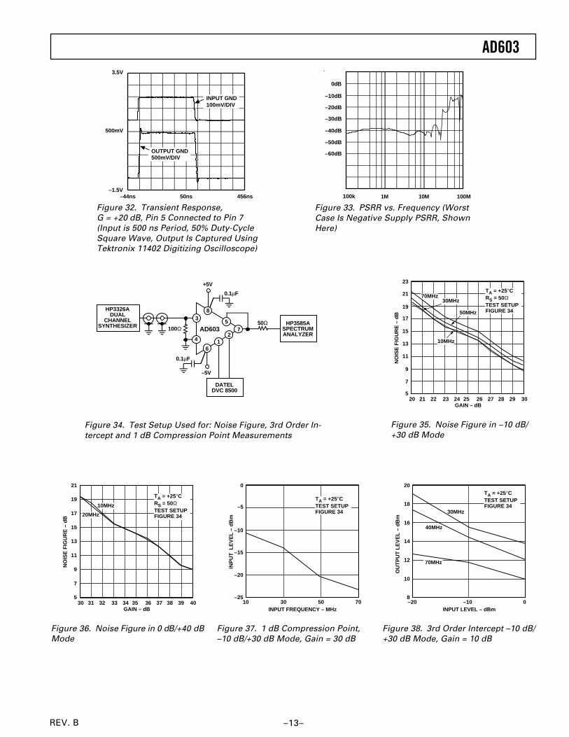
REV. B –13–
7
4
3
AD603HP3585A
SPECTRUMANALYZER
+5V
0.1µF
16
–5V
0.1µF
DATELDVC 8500
HP3326ADUAL
CHANNEL SYNTHESIZER 100Ω
2
5
8
50Ω
Figure 34. Test Setup Used for: Noise Figure, 3rd Order In-
tercept and 1 dB Compression Point Measurements
GAIN – dB
NO
ISE
FIG
UR
E –
dB
23
17
520 21 3022 23 24 25 26 27 28 29
21
19
13
9
15
11
TA = +25°CRS = 50ΩTEST SETUPFIGURE 34
70MHz
7
30MHz
50MHz
10MHz
Figure 35. Noise Figure in –10 dB/
+30 dB Mode
GAIN – dB
NO
ISE
FIG
UR
E –
dB
21
15
530 31 4032 33 34 35 36 37 38 39
19
17
11
7
13
9
TA = +25°CRS = 50ΩTEST SETUPFIGURE 34
10MHz
20MHz
Figure 36. Noise Figure in 0 dB/+40 dB
Mode
INPUT LEVEL – dBm
OU
TP
UT
LE
VE
L –
dB
m
20
18
8–20 –10 0
16
14
12
10
30MHz
40MHz
70MHz
TA = +25°CTEST SETUPFIGURE 34
Figure 38. 3rd Order Intercept –10 dB/
+30 dB Mode, Gain = 10 dB
INPUT FREQUENCY – MHz
INP
UT
LE
VE
L –
dB
m
0
–5
–2510 30 70
–10
–15
–20
TA = +25°CTEST SETUPFIGURE 34
50
Figure 37. 1 dB Compression Point,
–10 dB/+30 dB Mode, Gain = 30 dB
3.5V
–1.5V456ns–44ns
500mV
50ns
INPUT GND 100mV/DIV
OUTPUT GND 500mV/DIV
Figure 32. Transient Response,
G = +20 dB, Pin 5 Connected to Pin 7
(Input is 500 ns Period, 50% Duty-Cycle
Square Wave, Output Is Captured Using
Tektronix 11402 Digitizing Oscilloscope)
100k 1M 100M10M
–30dB
0dB
–10dB
–20dB
–60dB
–40dB
–50dB
Figure 33. PSRR vs. Frequency (Worst
Case Is Negative Supply PSRR, Shown
Here)
REV. B–14–
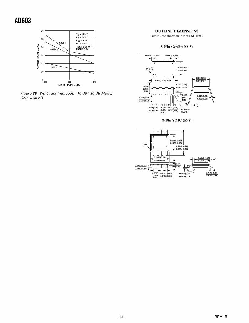
AD603
INPUT LEVEL – dBm
OU
TP
UT
LE
VE
L –
dB
m
20
18
8–40 –30 –20
16
14
12
10
30MHz
40MHz
70MHz
TA = +25°CRS = 50ΩRIN = 50ΩRL = 100ΩTEST SET-UPFIGURE 34
Figure 39. 3rd Order Intercept, –10 dB/+30 dB Mode,
Gain = 30 dB
OUTLINE DIMENSIONSDimensions shown in inches and (mm).
8-Pin Cerdip (Q-8)
0.320 (8.13)
0.290 (7.37)
0.015 (0.38)0.008 (0.20)
15°0°
0.005 (0.13) MIN 0.055 (1.4) MAX
1
PIN 1
4
58
0.310 (7.87)0.220 (5.59)
0.405 (10.29) MAX
0.200 (5.08)
MAX
SEATINGPLANE
0.023 (0.58)0.014 (0.36)
0.070 (1.78)0.030 (0.76)
0.060 (1.52)0.015 (0.38)
0.150(3.81)MIN
0.200 (5.08)0.125 (3.18)
0.100(2.54)BSC
8-Pin SOIC (R-8)
0.0098 (0.25)0.0075 (0.19)
0.0500 (1.27)0.0160 (0.41)
8°0°
0.0196 (0.50)0.0099 (0.25)
x 45°
PIN 1
0.1574 (4.00)0.1497 (3.80)
0.2440 (6.20)0.2284 (5.80)
4
5
1
8
0.0192 (0.49)0.0138 (0.35)
0.0500(1.27)BSC
0.0098 (0.25)
0.0040 (0.10)
0.1968 (5.00) 0.1890 (4.80)
0.102 (2.59)0.094 (2.39)

–15–

–16–
C1
85
1a
–1
0–5
/95
PR
INT
ED
IN
U.S
.A.