Embed Size (px)
Citation preview
A Vertical Bubble Flow Network using Inductive-
Coupling for 3D CMPs
Hiroki Matsutani1, Yasuhiro Take2, Daisuke Sasaki2,Masayuki Kimura2, Yuki Ono2, Yukinori Nishiyama2, Michihiro Koibuchi3, Tadahiro Kuroda2, Hideharu Amano2
1) The University of Tokyo, 2) Keio University,3) National Institute of Informatics
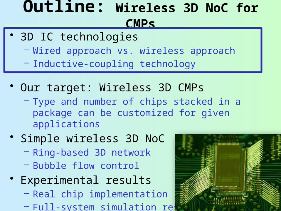
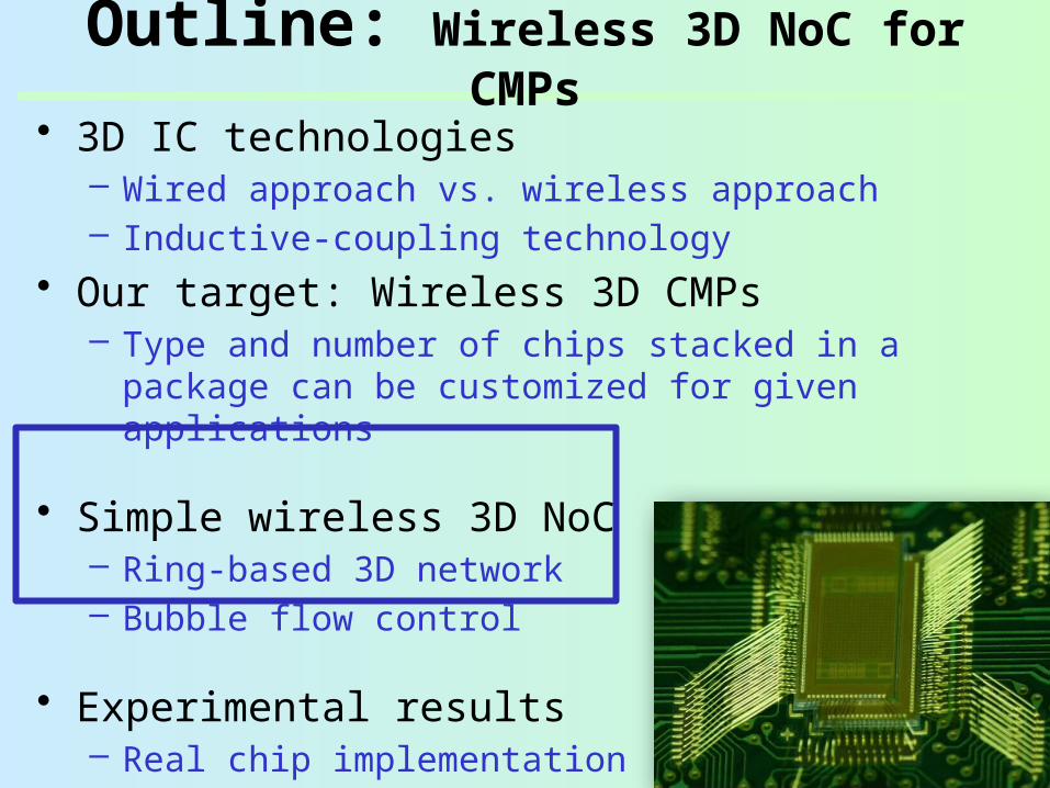
Outline: Wireless 3D NoC for CMPs
• 3D IC technologies– Wired approach vs. wireless approach– Inductive-coupling technology
• Our target: Wireless 3D CMPs– Type and number of chips stacked in a package
can be customized for given applications• Simple wireless 3D NoC
– Ring-based 3D network– Bubble flow control
• Experimental results– Real chip implementation– Full-system simulation results
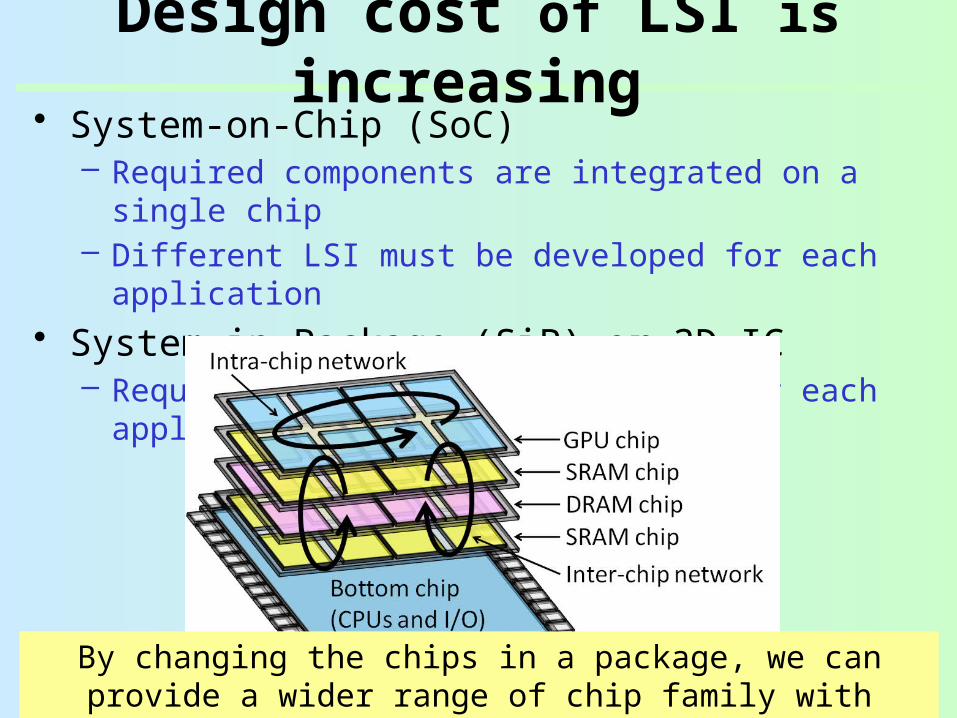
Design cost of LSI is increasing
• System-on-Chip (SoC)– Required components are integrated on a single
chip– Different LSI must be developed for each
application• System-in-Package (SiP) or 3D IC
– Required components are stacked for each application
By changing the chips in a package, we can provide a wider range of chip family with modest design cost
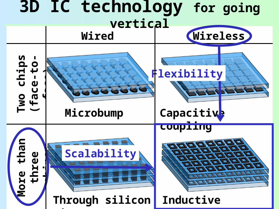
3D IC technology for going vertical
Two c
hip
s
(face-t
o-
face)
Microbump
Through silicon via
Capacitive coupling
Inductive coupling
Wired WirelessM
ore
th
an
th
ree
ch
ips
Flexibility
Scalability
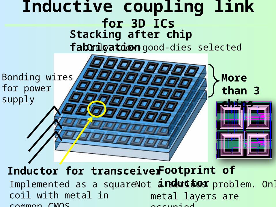
Inductive coupling link for 3D ICs
Stacking after chip fabricationOnly know-good-dies selected
Inductor for transceiverImplemented as a square coil with metal in common CMOS
Not a serious problem. Onlymetal layers are occupied
Footprint of inductor
Bonding wires for power supply
More than 3 chips
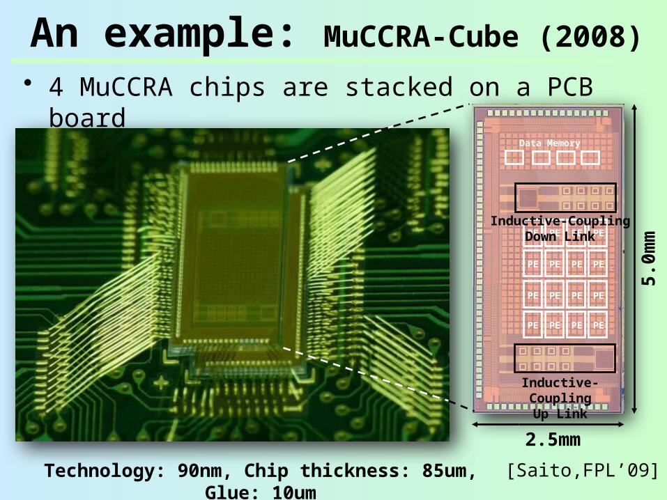
An example: MuCCRA-Cube (2008)
PE
PE
PE
PE
PE
PE
PE
PE
PE
PE
PE
PE
PE
PE
PE
PE
Data Memory
Technology: 90nm, Chip thickness: 85um, Glue: 10um
5.0
mm
2.5mm
Inductive-CouplingUp Link
Inductive-CouplingDown Link
• 4 MuCCRA chips are stacked on a PCB board
[Saito,FPL’09]
TX
TX
TX
TX TX
TX
TX
TXBonding wire
Bonding wire
Bonding wire
Bonding wire
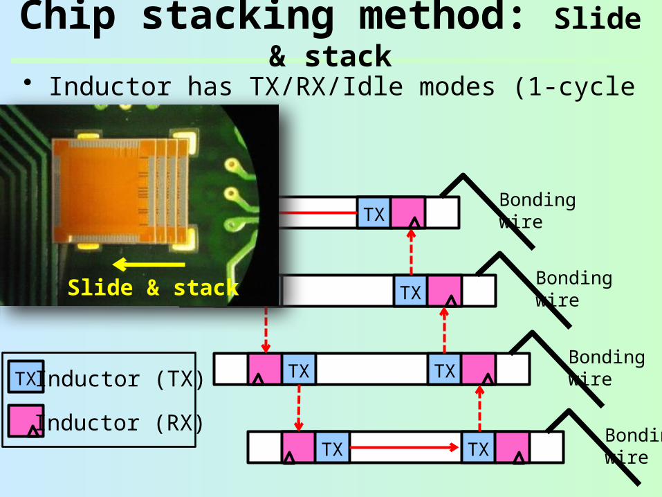
Chip stacking method: Slide & stack
• Inductor has TX/RX/Idle modes (1-cycle switch)
Slide & stack
Inductor (TX)
Inductor (RX)
TX
TX
TX
TX
TX TX
TX
TX
TXBonding wire
Bonding wire
Bonding wire
Bonding wire
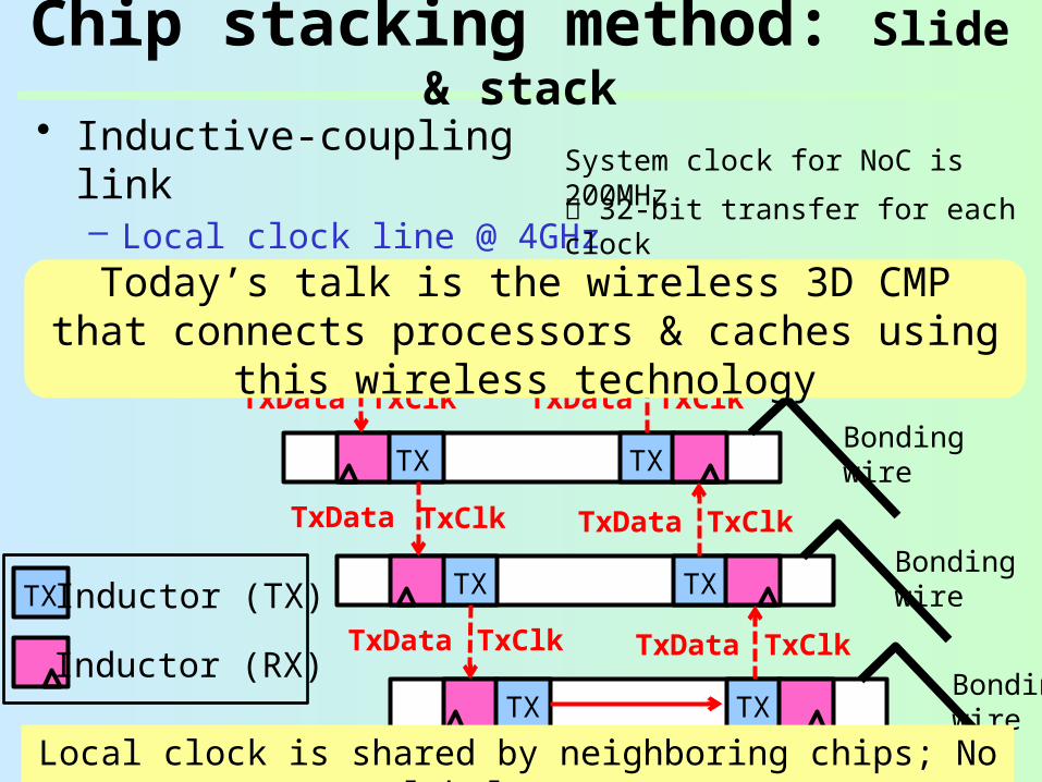
Chip stacking method: Slide & stack
• Inductive-coupling link– Local clock line @ 4GHz– Serial data line
Inductor (TX)
Inductor (RX)
TX
System clock for NoC is 200MHz 32-bit transfer for each clock
Local clock is shared by neighboring chips; No global sync.
TxData TxClk
TxData TxClk
TxData TxClk TxData TxClk
TxData TxClk
TxData TxClk
Today’s talk is the wireless 3D CMP that connects processors & caches using this
wireless technology
Outline: Wireless 3D NoC for CMPs
• 3D IC technologies– Wired approach vs. wireless approach– Inductive-coupling technology
• Our target: Wireless 3D CMPs– Type and number of chips stacked in a package
can be customized for given applications
• Simple wireless 3D NoC– Ring-based 3D network– Bubble flow control
• Experimental results– Real chip implementation– Full-system simulation results
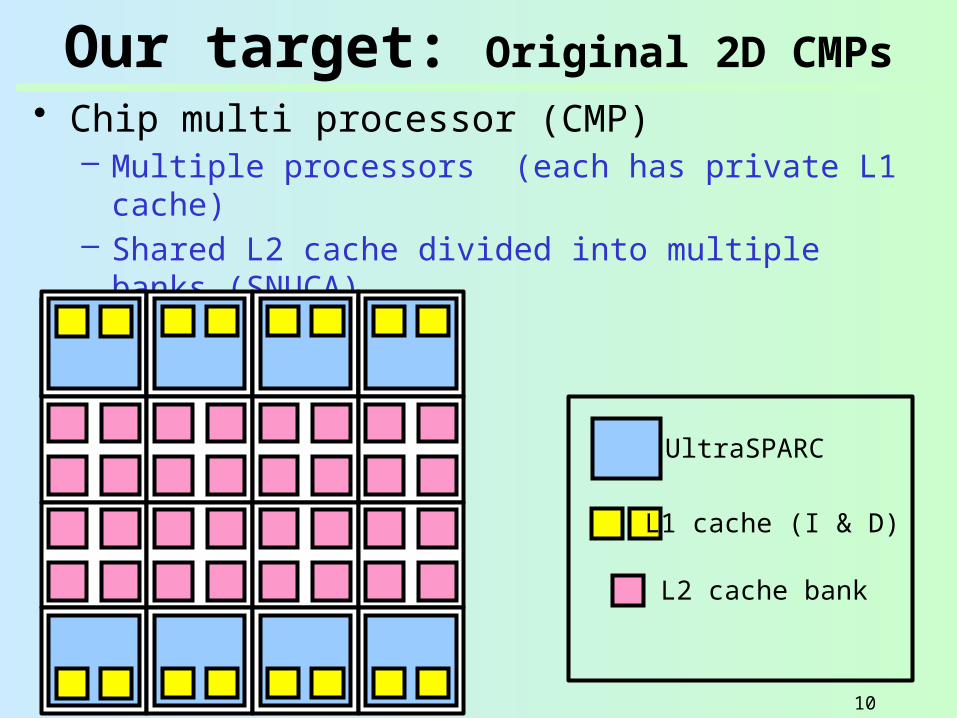
Our target: Original 2D CMPs• Chip multi processor (CMP)
– Multiple processors (each has private L1 cache)– Shared L2 cache divided into multiple banks
(SNUCA)
UltraSPARC
L1 cache (I & D)
L2 cache bank
Processor tile
Cache tile
10
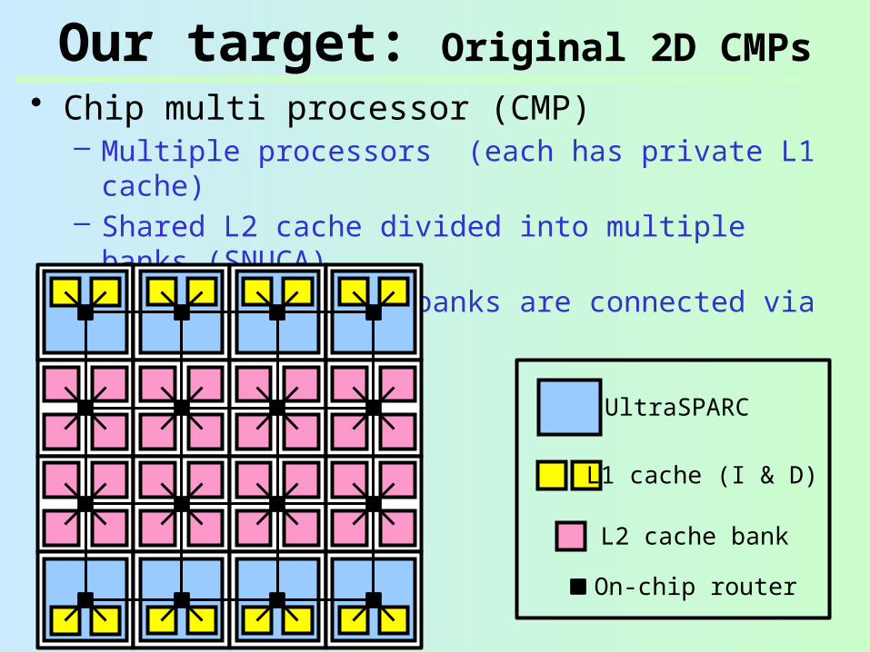
• Chip multi processor (CMP)– Multiple processors (each has private L1 cache)– Shared L2 cache divided into multiple banks
(SNUCA)– Processors and L2 banks are connected via NoC
On-chip router
Our target: Original 2D CMPs
UltraSPARC
L1 cache (I & D)
L2 cache bank
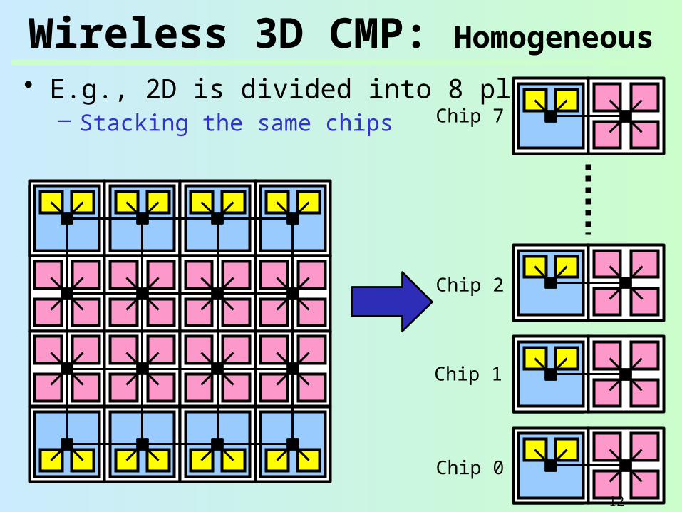
Wireless 3D CMP: Homogeneous
• E.g., 2D is divided into 8 planes– Stacking the same chips
Chip 0
Chip 1
Chip 2
Chip 7
12
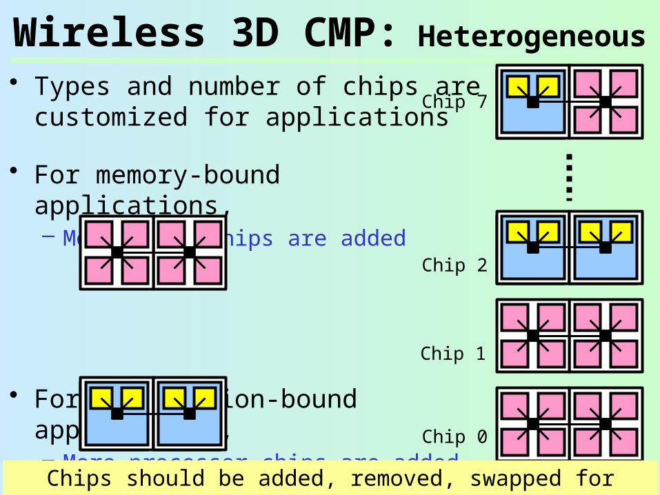
Wireless 3D CMP: Heterogeneous
• Types and number of chips are customized for applications
• For memory-bound applications,– More cache chips are added
• For computation-bound applications,– More processor chips are added
Chip 0
Chip 1
Chip 2
Chip 7
Chips should be added, removed, swapped for given application
Outline: Wireless 3D NoC for CMPs
• 3D IC technologies– Wired approach vs. wireless approach– Inductive-coupling technology
• Our target: Wireless 3D CMPs– Type and number of chips stacked in a package
can be customized for given applications
• Simple wireless 3D NoC– Ring-based 3D network– Bubble flow control
• Experimental results– Real chip implementation– Full-system simulation results
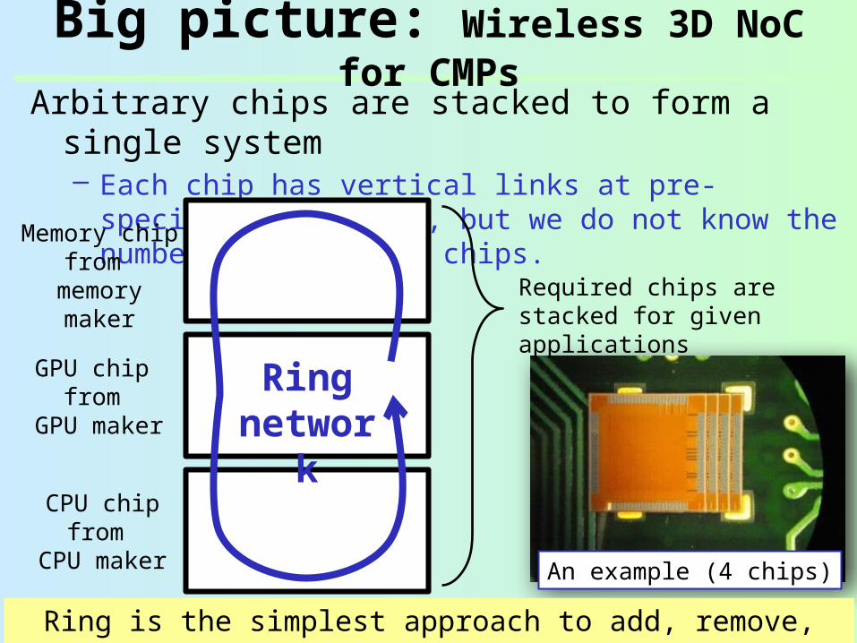
Big picture: Wireless 3D NoC for CMPs
Arbitrary chips are stacked to form a single system– Each chip has vertical links at pre-specified
locations, but we do not know the number and types of chips.
CPU chip from
CPU maker
Memory chip from
memory maker
GPU chip from
GPU maker
Required chips are stacked for given applications
An example (4 chips)
Ring is the simplest approach to add, remove, swap the nodes
Ring netwo
rk
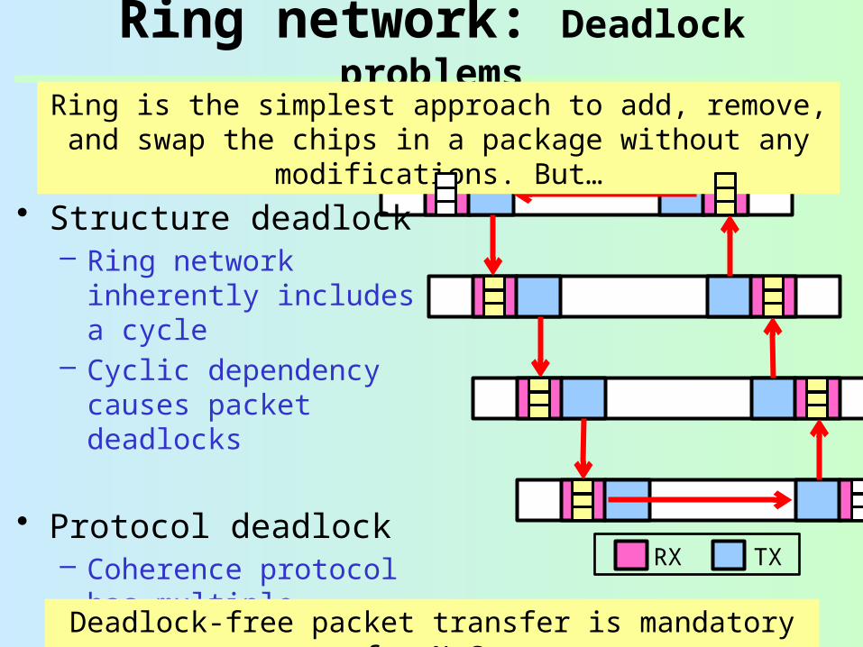
Ring network: Deadlock problems
Ring is the simplest approach to add, remove, and swap the chips in a package without any
modifications. But…• Structure deadlock
– Ring network inherently includes a cycle
– Cyclic dependency causes packet deadlocks
• Protocol deadlock– Coherence protocol has
multiple message classes
– Request-reply deadlocks
Deadlock-free packet transfer is mandatory for NoCs
RX TX
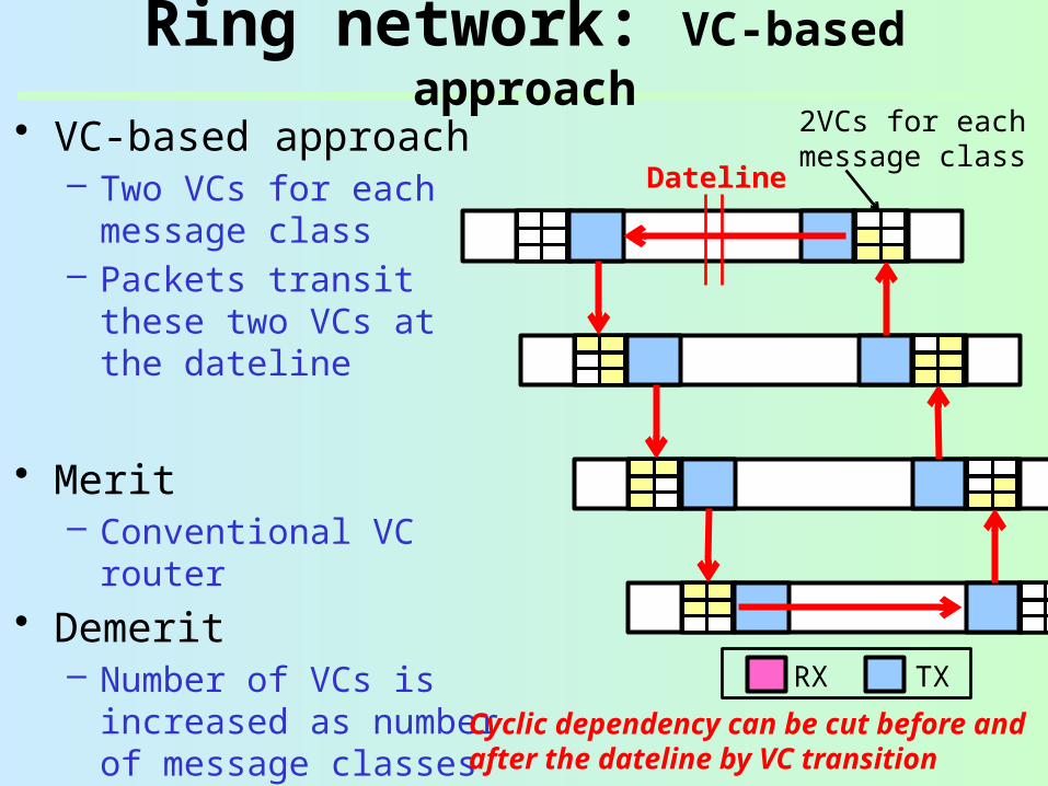
Ring network: VC-based approach
• VC-based approach– Two VCs for each
message class– Packets transit these
two VCs at the dateline
• Merit– Conventional VC router
• Demerit– Number of VCs is
increased as number of message classes
– 6 VCs for 3 classes
Dateline
2VCs for each message class
Cyclic dependency can be cut before and after the dateline by VC transition
RX TX
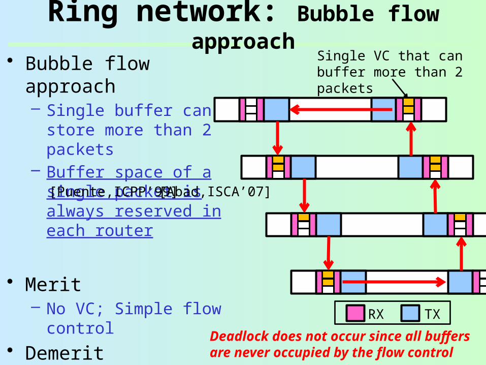
Ring network: Bubble flow approach
• Bubble flow approach– Single buffer can store
more than 2 packets– Buffer space of a single
packet is always reserved in each router
• Merit– No VC; Simple flow
control• Demerit
– Miss routing when packets cannot exit the ring
– Scalability problem
Single VC that can buffer more than 2 packets
Deadlock does not occur since all buffers are never occupied by the flow control
[Puente,ICPP’99] [Abad,ISCA’07]
RX TX
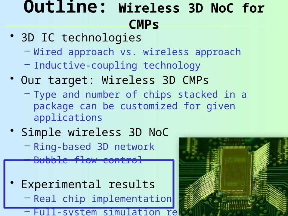
Outline: Wireless 3D NoC for CMPs
• 3D IC technologies– Wired approach vs. wireless approach– Inductive-coupling technology
• Our target: Wireless 3D CMPs– Type and number of chips stacked in a package
can be customized for given applications• Simple wireless 3D NoC
– Ring-based 3D network– Bubble flow control
• Experimental results– Real chip implementation– Full-system simulation results
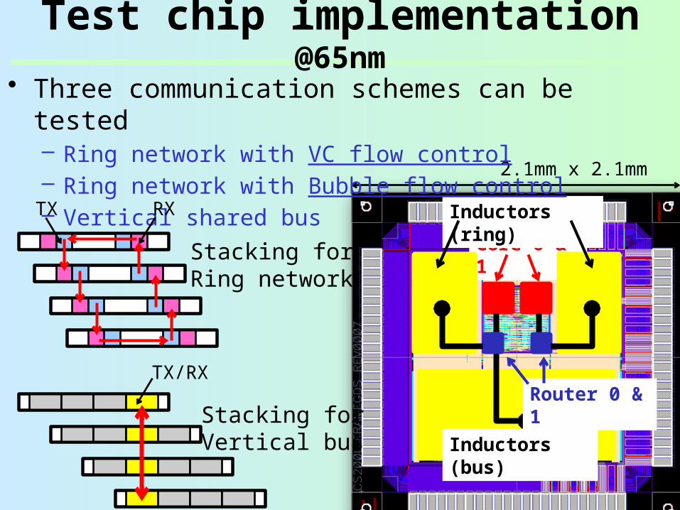
2.1mm x 2.1mm
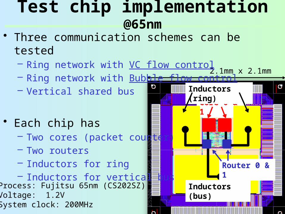
Test chip implementation @65nm
Core 0 & 1
Inductors (bus)
Inductors (ring)
Router 0 & 1
• Three communication schemes can be tested– Ring network with VC flow control– Ring network with Bubble flow control– Vertical shared bus
• Each chip has– Two cores (packet counter)– Two routers– Inductors for ring– Inductors for vertical bus
Process: Fujitsu 65nm (CS202SZ)Voltage: 1.2VSystem clock: 200MHz
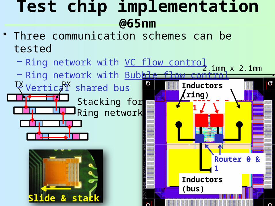
Test chip implementation @65nm
Core 0 & 1
Inductors (bus)
Inductors (ring)
Router 0 & 1
2.1mm x 2.1mm
• Three communication schemes can be tested– Ring network with VC flow control– Ring network with Bubble flow control– Vertical shared busTX
Stacking for Ring network
RX
Slide & stack
Test chip implementation @65nm
Core 0 & 1
Inductors (bus)
Inductors (ring)
Router 0 & 1
2.1mm x 2.1mm
• Three communication schemes can be tested– Ring network with VC flow control– Ring network with Bubble flow control– Vertical shared busTX
Stacking for Ring network
RX
TX/RX
Stacking for Vertical bus
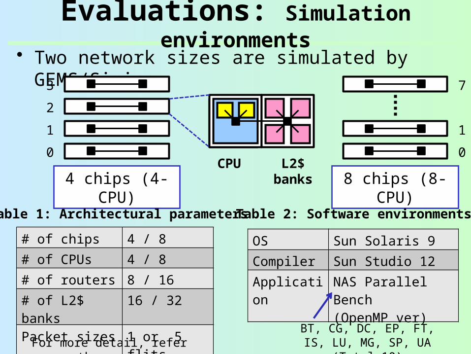
Evaluations: Simulation environments
• Two network sizes are simulated by GEMS/Simics
4 chips (4-CPU)
3
8 chips (8-CPU)
2
1
0CPU
L2$ banks
7
1
0
# of chips 4 / 8
# of CPUs 4 / 8
# of routers 8 / 16
# of L2$ banks
16 / 32
Packet sizes 1 or 5 flits
Table 1: Architectural parameters
OS Sun Solaris 9
Compiler Sun Studio 12
Application
NAS Parallel Bench(OpenMP ver)
Table 2: Software environments
BT, CG, DC, EP, FT, IS, LU, MG, SP, UA (Total 10)For more detail, refer the
paper
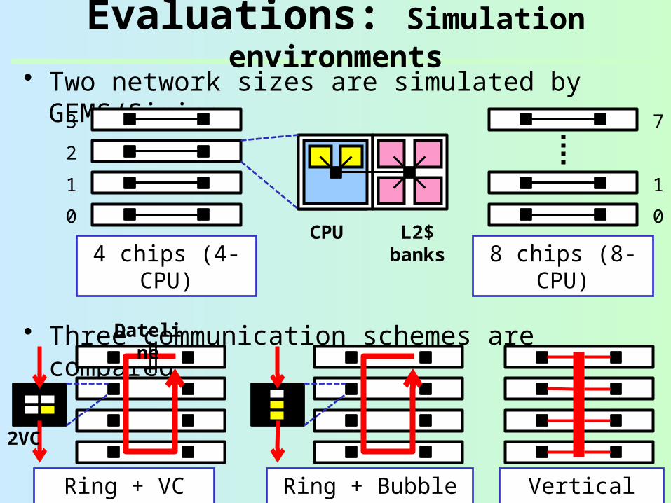
Evaluations: Simulation environments
• Two network sizes are simulated by GEMS/Simics
• Three communication schemes are compared
Ring + VC flow
Ring + Bubble flow
Vertical bus
4 chips (4-CPU)
3
8 chips (8-CPU)
2
1
0CPU
L2$ banks
7
1
0
Dateline
2VC
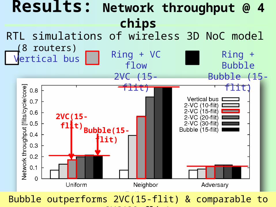
Results: Network throughput @ 4 chips
RTL simulations of wireless 3D NoC model (8 routers)
Bubble outperforms 2VC(15-flit) & comparable to 2VC(30-flit)
Vertical bus Ring + VC flow
2VC (15-flit)
Ring + BubbleBubble (15-
flit)
Bubble(15-flit)
2VC(15-flit)
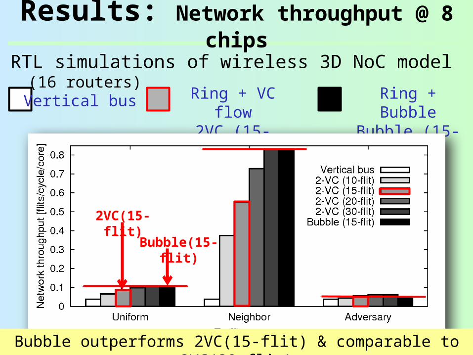
Results: Network throughput @ 8 chips
RTL simulations of wireless 3D NoC model (16 routers)Vertical bus Ring + VC
flow2VC (15-flit)
Ring + BubbleBubble (15-
flit)
Bubble(15-flit)
2VC(15-flit)
Bubble outperforms 2VC(15-flit) & comparable to 2VC(30-flit)
Bubble(15-flit)
2VC(15-flit)
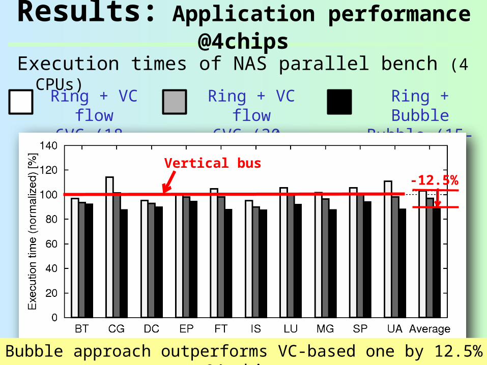
Results: Application performance @4chips
Execution times of NAS parallel bench (4 CPUs)
Ring + VC flow
6VC (30-flit)
Ring + BubbleBubble (15-
flit)
Ring + VC flow
6VC (18-flit)
Bubble approach outperforms VC-based one by 12.5% @4 chips
Vertical bus-12.5%
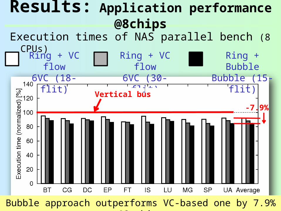
Results: Application performance @8chips
Execution times of NAS parallel bench (8 CPUs)
Ring + VC flow
6VC (30-flit)
Ring + BubbleBubble (15-
flit)
Ring + VC flow
6VC (18-flit)
Bubble approach outperforms VC-based one by 7.9% @8 chips
Vertical bus
-7.9%
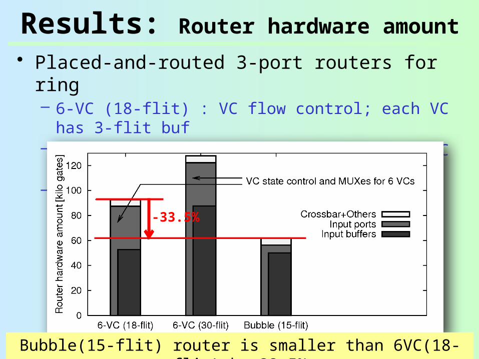
Results: Router hardware amount
• Placed-and-routed 3-port routers for ring– 6-VC (18-flit) : VC flow control; each VC has 3-flit
buf– 6-VC (30-flit) : VC flow control; each VC has 5-flit
buf– Bubble (15-flit) : Bubble flow control; single 15-flit
buf
Bubble(15-flit) router is smaller than 6VC(18-flit) by 33.5%
-33.5%
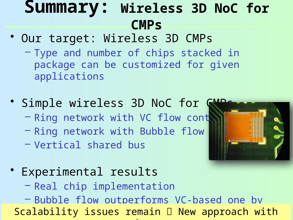
Summary: Wireless 3D NoC for CMPs
• Our target: Wireless 3D CMPs– Type and number of chips stacked in package can
be customized for given applications
• Simple wireless 3D NoC for CMPs– Ring network with VC flow control– Ring network with Bubble flow control– Vertical shared bus
• Experimental results– Real chip implementation– Bubble flow outperforms VC-based one by 7.9%-
12.5%– Bubble router is smaller than VC-based one by
33.5%Scalability issues remain New approach with spanning trees


![ソーシャルネットワークの グラフマイニング[Shiokawa 2015] Hiroaki Shiokawa, Yasuhiro Fujiwara, Makoto Onizuka: SCAN++: Efficient Algorithm for Finding Clusters,](https://img.pdfslide.tips/doc/110x75/5f44e63f4bdb0a0e601eb899/fffffffff-fffff-shiokawa-2015-hiroaki.jpg)