Embed Size (px)
Citation preview

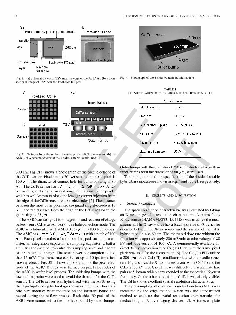
IEEE
Proo
f
IEEE TRANSACTIONS ON NUCLEAR SCIENCE, VOL. 56, NO. 4, AUGUST 2009 1
Development of 4-Sides Buttable CdTe-ASIC HybridModule for X-ray Flat Panel Detector
Mitsuru Tamaki, Yoshio Mito, Yasuhiro Shuto, Tatsuya Kiyuna, Masaya Yamamoto, Kenichi Sagae, Tooru Kina,Tatsuhiro Koizumi, and Ryoichi Ohno
Abstract—A 4-sides buttable CdTe-ASIC hybrid module suit-able for use in an X-ray flat panel detector (FPD) has been de-veloped by applying through silicon via (TSV) technology to thereadout ASIC. The ASIC has 128 256 channels of charge in-tegration type readout circuitry and an area of 12.9 mm 25.7mm. The CdTe sensor of 1 mm thickness, having the same areaand pixel of 100 � pitch, was fabricated from the Cl-doped CdTesingle crystal grown by traveling heater method (THM). Then theCdTe pixel sensor was hybridized with the ASIC using the bump-bonding technology. The basic performance of this 4-sides buttablemodule was evaluated by taking X-ray images, and it was com-pared with that of a commercially available indirect type CsI(Tl)FPD. A prototype CdTe FPD was made by assembling 9 pieces ofthe 4-sides buttable modules into 3 3 arrays in which the neigh-boring modules were mounted on the interface board. The FPDcovers an active area of 77 mm 39 mm. The results showed thegreat potential of this 4-sides buttable module for the new real timeX-ray FPD with high spatial resolution.
Index Terms—CdTe, four-sides buttable, through-silicon-via,X-ray imaging.
I. INTRODUCTION
C ADMIUM TELLURIDE (CdTe) is a promising materialfor X-ray imaging detectors in the field of the medical,
dental and nondestructive testing applications because of thehigh detective quantum efficiency and high energy resolutionfor X-ray. Various types of CdTe-ASIC hybrid modules hadbeen already developed for X-ray imaging [1], [2]. Fig. 1(a)shows a schematic view of the structure for conventional CdTe-ASIC hybrid module. However, as long as they use the ASICwith conventional structure where the I/O pads are arrangedalong one edge of the ASIC to be wire-bonded to an interfaceboard, the I/O pads area of the ASIC causes an inevitable deadspace for plural hybrid modules to be assembled adjoining eachother. After all, this structure of the so-called 3-sides buttableCdTe-ASIC hybrid modules has restricted the arrangement ofthe modules for a two-dimensional X-ray imager.
By eliminating the wire-bonding and the dead space fromthe conventional structure, an active area of the CdTe sensorcan be extended up to the edge of the ASIC shown in Fig. 1(b).The so-called 4-sides buttable structure is realized by using
Manuscript received November 13, 2008; revised March 04, 2009 and May19, 2009.
The authors are with ACRORAD Co., Ltd., Okinawa 904-2234, Japan(e-mail: [email protected]).
Digital Object Identifier 10.1109/TNS.2009.2024417
Fig. 1. Structure of (a) the conventional CdTe-ASIC hybrid module and (b) the4-sides buttable CdTe-ASIC hybrid module.
these modules which can be assembled in all four directions. Inthis work, we describe the development of the 4-sides buttableCdTe-ASIC hybrid module for a Flat Panel Detector (FPD).
II. MATERIAL AND METHOD
A. Through Silicon Via (TSV)
Through Silicon Via (TSV) technology, which has been re-cently developed for the advanced Silicon devices having three-dimensional stacking structure, was applied to the readout pixelASIC to eliminate the wire-bonding and the dead space from3-sides buttable module. Fig. 2 shows (a) a schematic view ofTSV near the edge of the ASIC and (b) a cross sectional imageof TSV near the front-side I/O pad. Via holes were etched fromthe back-side of ASIC to reach the front-side I/O pad. The di-ameter and the depth of via hole are 80 and 250 , re-spectively. The oxide insulation layer and the conductive layerwere formed on the sidewall of via and they were extended to beconnected to the new back-side I/O pads of the ASIC. The sur-face of the ASIC was protected by the passivation layer. Totalnumber of I/O pads and via holes is 26 which are formed alongone edge of the ASIC chip and they are divided into analog anddigital lines which have the function of GND, analog output,ASIC configuration, power supply, clock, and tuning. The fab-rication of TSV was carried out in a Silicon MEMS foundry.
B. Hybridization
The CdTe sensor was fabricated from the Cl-doped CdTesingle crystal grown by Traveling Heater Method (THM) [3],[4]. CdTe single crystal wafers of 1 mm thickness were slicedfrom CdTe ingot with (111) orientation and polished mechani-cally and chemically. The Schottky contact was formed on CdTewafers using indium (In) as a common electrode and platinum(Pt) as pixel electrodes. The thickness of the indium layer is
0018-9499/$26.00 © 2009 IEEE
IEEE
Proo
f
2 IEEE TRANSACTIONS ON NUCLEAR SCIENCE, VOL. 56, NO. 4, AUGUST 2009
Fig. 2. (a) Schematic view of TSV near the edge of the ASIC and (b) a crosssectional image of TSV near the front-side I/O pad.
Fig. 3. Photographs of the surface of (a) the pixelized CdTe sensor and (b) theASIC. (c) A schematic view of the 4-sides buttable hybrid module.
300 nm. Fig. 3(a) shows a photograph of the pixel electrode ofthe CdTe sensor. Pixel size is 70 square and pixel pitch is100 . The diameter of contact hole for bump bonding is 30
. The CdTe sensor has . A 15--wide guard ring is formed surrounding most outer pixels,
which is well known to block the leakage current injection fromthe edge of the CdTe sensor to pixel electrodes [5]. The distancebetween the most outer pixel and the guard ring electrode is 15
, and the distance from the edge of the CdTe sensor to theguard ring is 25 .
The ASIC was designed for integration and read out of chargepulses from a CdTe sensor working in hole collection mode. TheASIC was fabricated with AMIS 0.35- CMOS technology.The ASIC has with a pitch of 100
. Each pixel contains a bump bonding pad, an input tran-sistor, an integration capacitor, a sampling capacitor, a bufferamplifier and switches to control the sampling, reset and readoutof the integrated charge. The total power consumption is lessthan 15 mW. The frame rate can be set up to 50 fps for a fastmoving object. Fig. 3(b) shows a photograph of the pixel elec-trode of the ASIC. Bumps were formed on pixel electrodes ofthe ASIC in wafer level process. The soldering bumps with thelow melting point were used to avoid the damage for the CdTesensor. The CdTe sensor was hybridized with the ASIC usingthe flip-chip-bonding technology shown in Fig. 3(c). These hy-brid bare modules were mounted on the interface board andheated during the re-flow process. Back side I/O pads of theASIC were connected to the interface board by outer bumps.
Fig. 4. Photograph of the 4-sides buttable hybrid module.
TABLE ITHE SPECIFICATIONS OF THE 4-SIDES BUTTABLE HYBRID MODULE
Outer bumps with the diameter of 750 , which are larger thaninner bumps with the diameter of 60 , were used.
The photograph and the specification of the 4-sides buttablehybrid bare module are shown in Fig. 4 and Table I, respectively.
III. RESULTS AND DISCUSSTION
A. Spatial Resolution
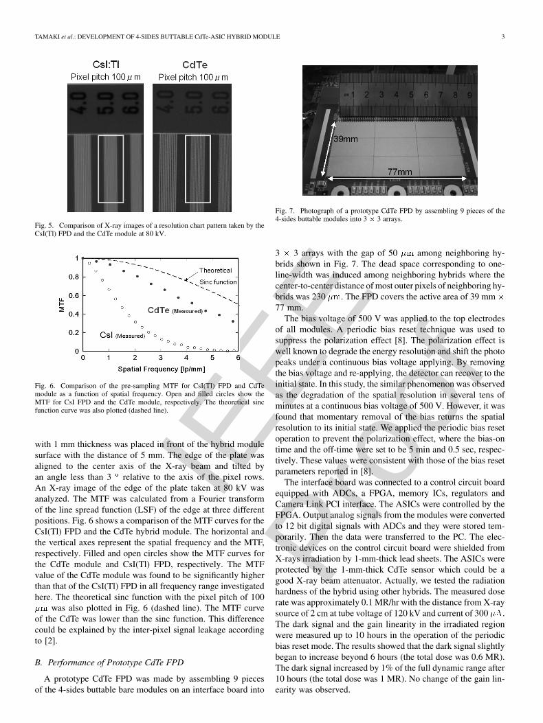
The spatial resolution characteristic was evaluated by takingan X-ray image of a resolution chart pattern. A micro focusX-ray source (HAMAMATSU L9181S) was used for the mea-surement. The X-ray source has a focal spot size of 40 . Thedistance between the X-ray source and the surface of the CdTehybrid module was 60 cm. The measured dose rate without thefiltration was approximately 800 mR/min at tube voltage of 80kV and tube current of 100 . A commercially available in-direct X-ray conversion type CsI(Tl) FPD with the same pixelpitch was used for the comparison [6]. The CsI(Tl) FPD utilizea 200- -thick CsI (Tl) scintillator plate with a needle struc-ture. Fig. 5 shows the X-ray images taken by the CsI(Tl) and theCdTe at 80 kV. For CsI(Tl), it was difficult to discriminate linepairs at 5 lp/mm which corresponded to the theoretical Nyquistfrequency. On the other hand, for the CdTe it was clearly visible.The CdTe shows excellent spatial resolution characteristics.
The pre-sampling Modulation Transfer Function (MTF) wasmeasured by the edge method which was the standardizedmethod to evaluate the spatial resolution characteristics formedical digital X-ray imaging devices [7]. A tungsten plate
IEEE
Proo
f
TAMAKI et al.: DEVELOPMENT OF 4-SIDES BUTTABLE CdTe-ASIC HYBRID MODULE 3
Fig. 5. Comparison of X-ray images of a resolution chart pattern taken by theCsI(Tl) FPD and the CdTe module at 80 kV.
Fig. 6. Comparison of the pre-sampling MTF for CsI(Tl) FPD and CdTemodule as a function of spatial frequency. Open and filled circles show theMTF for CsI FPD and the CdTe module, respectively. The theoretical sincfunction curve was also plotted (dashed line).
with 1 mm thickness was placed in front of the hybrid modulesurface with the distance of 5 mm. The edge of the plate wasaligned to the center axis of the X-ray beam and tilted byan angle less than 3 relative to the axis of the pixel rows.An X-ray image of the edge of the plate taken at 80 kV wasanalyzed. The MTF was calculated from a Fourier transformof the line spread function (LSF) of the edge at three differentpositions. Fig. 6 shows a comparison of the MTF curves for theCsI(Tl) FPD and the CdTe hybrid module. The horizontal andthe vertical axes represent the spatial frequency and the MTF,respectively. Filled and open circles show the MTF curves forthe CdTe module and CsI(Tl) FPD, respectively. The MTFvalue of the CdTe module was found to be significantly higherthan that of the CsI(Tl) FPD in all frequency range investigatedhere. The theoretical sinc function with the pixel pitch of 100
was also plotted in Fig. 6 (dashed line). The MTF curveof the CdTe was lower than the sinc function. This differencecould be explained by the inter-pixel signal leakage accordingto [2].
B. Performance of Prototype CdTe FPD
A prototype CdTe FPD was made by assembling 9 piecesof the 4-sides buttable bare modules on an interface board into
Fig. 7. Photograph of a prototype CdTe FPD by assembling 9 pieces of the4-sides buttable modules into 3 � 3 arrays.
3 3 arrays with the gap of 50 among neighboring hy-brids shown in Fig. 7. The dead space corresponding to one-line-width was induced among neighboring hybrids where thecenter-to-center distance of most outer pixels of neighboring hy-brids was 230 . The FPD covers the active area of 39 mm77 mm.
The bias voltage of 500 V was applied to the top electrodesof all modules. A periodic bias reset technique was used tosuppress the polarization effect [8]. The polarization effect iswell known to degrade the energy resolution and shift the photopeaks under a continuous bias voltage applying. By removingthe bias voltage and re-applying, the detector can recover to theinitial state. In this study, the similar phenomenon was observedas the degradation of the spatial resolution in several tens ofminutes at a continuous bias voltage of 500 V. However, it wasfound that momentary removal of the bias returns the spatialresolution to its initial state. We applied the periodic bias resetoperation to prevent the polarization effect, where the bias-ontime and the off-time were set to be 5 min and 0.5 sec, respec-tively. These values were consistent with those of the bias resetparameters reported in [8].
The interface board was connected to a control circuit boardequipped with ADCs, a FPGA, memory ICs, regulators andCamera Link PCI interface. The ASICs were controlled by theFPGA. Output analog signals from the modules were convertedto 12 bit digital signals with ADCs and they were stored tem-porarily. Then the data were transferred to the PC. The elec-tronic devices on the control circuit board were shielded fromX-rays irradiation by 1-mm-thick lead sheets. The ASICs wereprotected by the 1-mm-thick CdTe sensor which could be agood X-ray beam attenuator. Actually, we tested the radiationhardness of the hybrid using other hybrids. The measured doserate was approximately 0.1 MR/hr with the distance from X-raysource of 2 cm at tube voltage of 120 kV and current of 300 .The dark signal and the gain linearity in the irradiated regionwere measured up to 10 hours in the operation of the periodicbias reset mode. The results showed that the dark signal slightlybegan to increase beyond 6 hours (the total dose was 0.6 MR).The dark signal increased by 1% of the full dynamic range after10 hours (the total dose was 1 MR). No change of the gain lin-earity was observed.
IEEE
Proo
f
4 IEEE TRANSACTIONS ON NUCLEAR SCIENCE, VOL. 56, NO. 4, AUGUST 2009
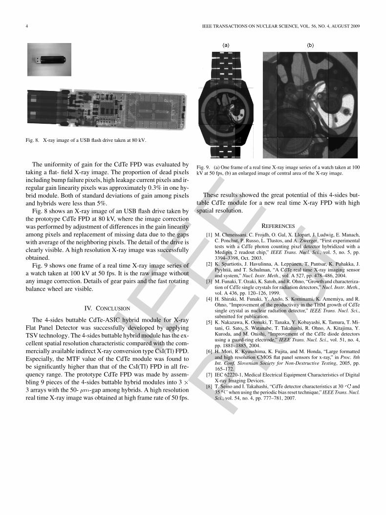
Fig. 8. X-ray image of a USB flash drive taken at 80 kV.
The uniformity of gain for the CdTe FPD was evaluated bytaking a flat- field X-ray image. The proportion of dead pixelsincluding bump failure pixels, high leakage current pixels and ir-regular gain linearity pixels was approximately 0.3% in one hy-brid module. Both of standard deviations of gain among pixelsand hybrids were less than 5%.
Fig. 8 shows an X-ray image of an USB flash drive taken bythe prototype CdTe FPD at 80 kV, where the image correctionwas performed by adjustment of differences in the gain linearityamong pixels and replacement of missing data due to the gapswith average of the neighboring pixels. The detail of the drive isclearly visible. A high resolution X-ray image was successfullyobtained.
Fig. 9 shows one frame of a real time X-ray image series ofa watch taken at 100 kV at 50 fps. It is the raw image withoutany image correction. Details of gear pairs and the fast rotatingbalance wheel are visible.
IV. CONCLUSION
The 4-sides buttable CdTe-ASIC hybrid module for X-rayFlat Panel Detector was successfully developed by applyingTSV technology. The 4-sides buttable hybrid module has the ex-cellent spatial resolution characteristic compared with the com-mercially available indirect X-ray conversion type CsI(Tl) FPD.Especially, the MTF value of the CdTe module was found tobe significantly higher than that of the CsI(Tl) FPD in all fre-quency range. The prototype CdTe FPD was made by assem-bling 9 pieces of the 4-sides buttable hybrid modules into 33 arrays with the 50- -gap among hybrids. A high resolutionreal time X-ray image was obtained at high frame rate of 50 fps.
Fig. 9. (a) One frame of a real time X-ray image series of a watch taken at 100kV at 50 fps, (b) an enlarged image of central area of the X-ray image.
These results showed the great potential of this 4-sides but-table CdTe module for a new real time X-ray FPD with highspatial resolution.
REFERENCES
[1] M. Chmeissani, C. Frojdh, O. Gal, X. Llopart, J. Ludwig, E. Manach,C. Ponchut, P. Russo, L. Tlustos, and A. Zwerger, “First experimentaltests with a CdTe photon counting pixel detector hybridized with aMedipix 2 readout chip,” IEEE Trans. Nucl. Sci., vol. 5, no. 5, pp.3394–3398, Oct. 2003.
[2] K. Spartiotis, J. Havulinna, A. Leppänen, T. Pantsar, K. Puhakka, J.Pyyhtiä, and T. Schulman, “A CdTe real time X-ray imaging sensorand system,” Nucl. Instr. Meth., vol. A 527, pp. 478–486, 2004.
[3] M. Funaki, T. Ozaki, K. Satoh, and R. Ohno, “Growth and characteriza-tion of CdTe single crystals for radiation detectors,” Nucl. Instr. Meth.,vol. A 436, pp. 120–126, 1999.
[4] H. Shiraki, M. Funaki, Y. Ando, S. Kominami, K. Amemiya, and R.Ohno, “Improvement of the productivity in the THM growth of CdTesingle crystal as nuclear radiation detector,” IEEE Trans. Nucl. Sci.,submitted for publication.
[5] K. Nakazawa, K. Oonuki, T. Tanaka, Y. Kobayashi, K. Tamura, T. Mi-tani, G. Sato, S. Watanabe, T. Takahashi, R. Ohno, A. Kitajima, Y.Kuroda, and M. Onishi, “Improvement of the CdTe diode detectorsusing a guard-ring electrode,” IEEE Trans. Nucl. Sci., vol. 51, no. 4,pp. 1881–1885, 2004.
[6] H. Mori, R. Kyuushima, K. Fujita, and M. Honda, “Large formattedand high resolution CMOS flat panel sensors for x-ray,” in Proc. 8thInt. Conf. Slovenian Society for Non-Destructive Testing, 2005, pp.165–172.
[7] IEC 62220-1, Medical Electrical Equipment Characteristics of DigitalX-ray Imaging Devices.
[8] T. Seino and I. Takahashi, “CdTe detector characteristics at 30 � and35 �when using the periodic bias reset technique,” IEEE Trans. Nucl.Sci., vol. 54, no. 4, pp. 777–781, 2007.