Embed Size (px)
Citation preview
Published: February 03, 2011
r 2011 American Chemical Society 1002 dx.doi.org/10.1021/nl103814g |Nano Lett. 2011, 11, 1002–1008
LETTER
pubs.acs.org/NanoLett
Quantum Dot Size Dependent J-V Characteristics in HeterojunctionZnO/PbS Quantum Dot Solar CellsJianbo Gao,†,‡ Joseph M. Luther,† Octavi E. Semonin,†,§ Randy J. Ellingson,‡ Arthur J. Nozik,†,§ andMatthew C. Beard*,†
†Chemical and Material Sciences Center, National Renewable Energy Laboratory, Golden, Colorado 80401, United States‡Department of Physics and Astronomy, Wright Center for Photovoltaics Innovation and Commercialization, University of Toledo,Toledo, Ohio 43606, United States§Department of Chemistry and Biochemistry, University of Colorado at Boulder, Boulder, Colorado 80309, United States
bS Supporting Information
ABSTRACT: The current-voltage (J-V) characteristics ofZnO/PbS quantum dot (QD) solar cells show a QD size-dependent behavior resulting from a Schottky junction thatforms at the back metal electrode opposing the desirablediode formed between the ZnO and PbSQD layers. We studya QD size-dependent roll-over effect that refers to thesaturation of photocurrent in forward bias and crossovereffect which occurs when the light and dark J-V curvesintersect.Wemodel the J-V characteristics with amain diodeformed between the n-type ZnO nanocrystal (NC) layer andp-type PbS QD layer in series with a leaky Schottky-diode formed between PbS QD layer and metal contact. We show how thecharacteristics of the two diodes depend on QD size, metal work function, and PbS QD layer thickness, and we discuss how thepresence of the back diode complicates finding an optimal layer thickness. Finally, we present Kelvin probe measurements todetermine the Fermi level of the QD layers and discuss band alignment, Fermi-level pinning, and the Voc within these devices.
KEYWORDS: Quantum Dots, solar cells, heterojunction, double diode, PbS
Schottky-junction quantum dot solar cells (QDSCs) haveattracted intense attention in the past few years,1-4 but they
have several limitations. While large short circuit currents (Jsc) ofover 20 mA/cm2 are achieved, the open circuit voltage (Voc) islow compared to the band gap energy, Eg. The maximum Voc
obtainable in a Schottky geometry is likely limited to Eg/2q,where q is the charge of an electron. The low Voc’s typicallyreported are attributed to Fermi-level pinning at the metal/semiconductor junction. Because the Schottky junction forms atthe back electrode opposite fromwhere light is incident, minoritycarriers (electrons) recombine or are trapped at defect sitesbefore they reach the negative electrode. To overcome the abovelimitations, an “inverted cell” structure can be used, where light isincident upon the high-field region that forms at the heterojunc-tion of a transparent n-type metal oxide layer with the p-type PbSQD layer.5-8 Here, minority carriers should flow toward themetal oxide while holes are extracted at the high work functionback contact. In this structure, the Voc is determined by thedifference in the quasi-Fermi levels in the PbS QD and ZnOlayers. We recently reported an NREL-certified ∼3% efficientdevice with structure of ITO/ZnO NC/PbS QD/Au with a Voc
that is greater than the PbS bulk band gap, demonstrating thatquantum confinement effects can be utilized in QDSCs.7 Thedevice is remarkably stable in air without encapsulation for morethan 1000 h. However, a full understanding of exciton dissociation
and space charge within the device is lacking. There is ampleroom for improvement in all three key factors that impactefficiency: Jsc, Voc, and fill factor (FF). Here we analyze thesize-dependent J-V characteristics and discuss limiting factors ofthe device architecture with suggested routes for improvement.
We focus on ITO/ZnO NC/PbS QD/metal devices fabri-cated in air with eight different diameters of PbS QD with firstexciton transition energies (effective band gaps) ranging from0.76 to 2.1 eV. ZnO NC layers were spin coated at 2000 rpmfrom chloroform onto a cleaned glass substrate with prepat-terned ITO electrodes of 150 nm thickness (Thin Film Devices,Anaheim). The resulting∼100 nm thick ZnO layer composed of∼5 nm nanocrystals was heated on a hot plate set to 260 �C for30 min to remove residual solvent. The PbS QD layer wasdeposited onto the ZnO layer via sequentially immersing thesubstrate into a PbS QD hexane solution of concentration10 mg/mL followed by 1 mM 1,2-ethanedithiol (EDT) in ace-tonitrile solution.1,5,9 Approximately 30 dipping cycles wererequired to produce QD layer thicknesses of 200-270 nm.The film growth rate is fairly linear with the number of dip cyclesand depends primarily on the QD concentration.10 Au or Ag is
Received: October 29, 2010Revised: January 4, 2011
1003 dx.doi.org/10.1021/nl103814g |Nano Lett. 2011, 11, 1002–1008
Nano Letters LETTER
evaporated onto the top of the film at a rate of 0.1 nm/s with basepressure of 1�10-7 Torr to produce∼100 nm layers. All devicesare formed with an active area of 0.11 cm2 defined by the overlapof the contact electrodes. Synthesis of the ZnO NCs and PbSQDs followed previous published reports,5 and more detailedinformation concerning layer thickness and QD diameters isprovided in the Supporting Information.
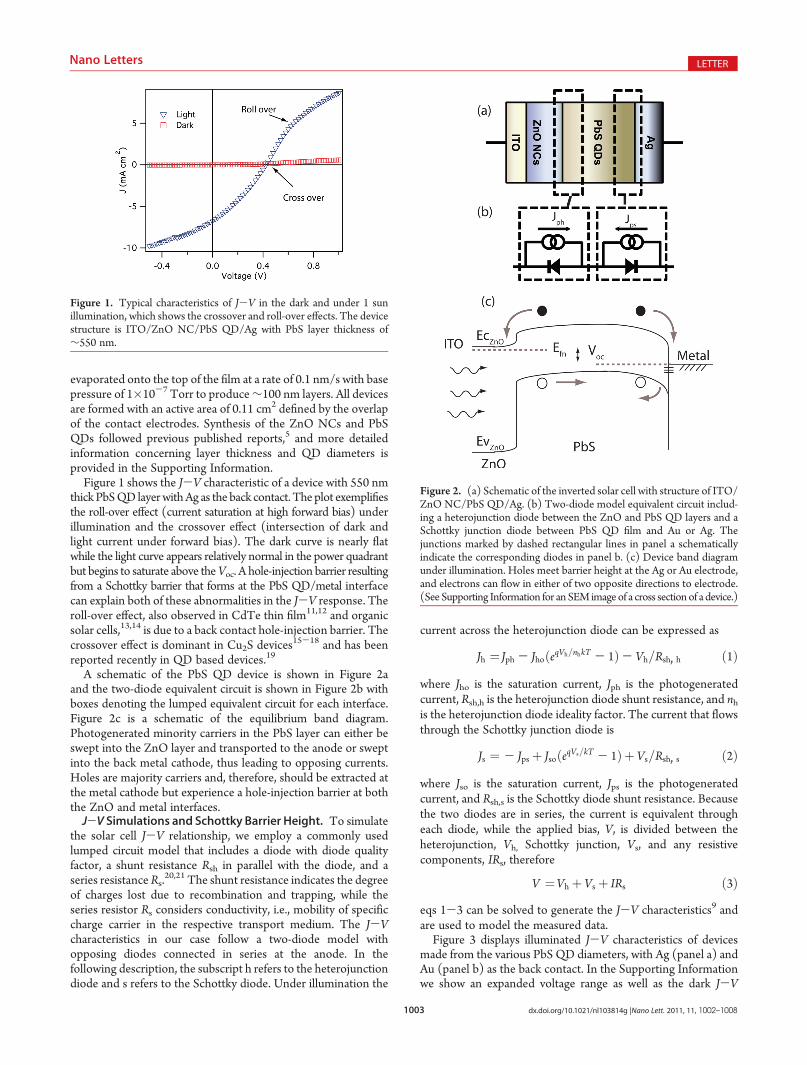
Figure 1 shows the J-V characteristic of a device with 550 nmthickPbSQD layerwithAg as the back contact. The plot exemplifiesthe roll-over effect (current saturation at high forward bias) underillumination and the crossover effect (intersection of dark andlight current under forward bias). The dark curve is nearly flatwhile the light curve appears relatively normal in the power quadrantbut begins to saturate above theVoc. A hole-injection barrier resultingfrom a Schottky barrier that forms at the PbS QD/metal interfacecan explain both of these abnormalities in the J-V response. Theroll-over effect, also observed in CdTe thin film11,12 and organicsolar cells,13,14 is due to a back contact hole-injection barrier. Thecrossover effect is dominant in Cu2S devices
15-18 and has beenreported recently in QD based devices.19
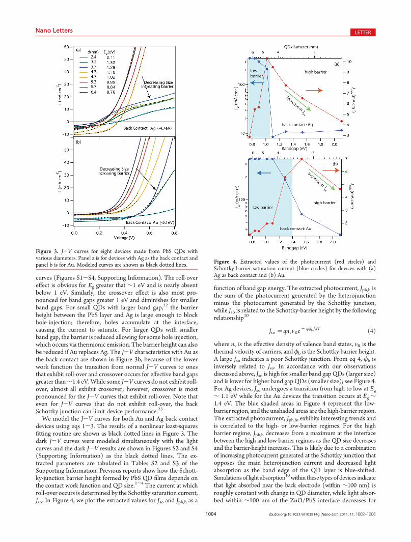
A schematic of the PbS QD device is shown in Figure 2aand the two-diode equivalent circuit is shown in Figure 2b withboxes denoting the lumped equivalent circuit for each interface.Figure 2c is a schematic of the equilibrium band diagram.Photogenerated minority carriers in the PbS layer can either beswept into the ZnO layer and transported to the anode or sweptinto the back metal cathode, thus leading to opposing currents.Holes are majority carriers and, therefore, should be extracted atthe metal cathode but experience a hole-injection barrier at boththe ZnO and metal interfaces.J-V Simulations and Schottky Barrier Height. To simulate
the solar cell J-V relationship, we employ a commonly usedlumped circuit model that includes a diode with diode qualityfactor, a shunt resistance Rsh in parallel with the diode, and aseries resistanceRs.
20,21 The shunt resistance indicates the degreeof charges lost due to recombination and trapping, while theseries resistor Rs considers conductivity, i.e., mobility of specificcharge carrier in the respective transport medium. The J-Vcharacteristics in our case follow a two-diode model withopposing diodes connected in series at the anode. In thefollowing description, the subscript h refers to the heterojunctiondiode and s refers to the Schottky diode. Under illumination the
current across the heterojunction diode can be expressed as
Jh ¼ Jph - JhoðeqVh=nhkT - 1Þ- Vh=Rsh, h ð1Þwhere Jho is the saturation current, Jph is the photogeneratedcurrent, Rsh,h is the heterojunction diode shunt resistance, and nhis the heterojunction diode ideality factor. The current that flowsthrough the Schottky junction diode is
Js ¼ - Jps þ JsoðeqVs=kT - 1ÞþVs=Rsh, s ð2Þwhere Jso is the saturation current, Jps is the photogeneratedcurrent, and Rsh,s is the Schottky diode shunt resistance. Becausethe two diodes are in series, the current is equivalent througheach diode, while the applied bias, V, is divided between theheterojunction, Vh, Schottky junction, Vs, and any resistivecomponents, IRs, therefore
V ¼Vh þVs þ IRs ð3Þeqs 1-3 can be solved to generate the J-V characteristics9 andare used to model the measured data.Figure 3 displays illuminated J-V characteristics of devices
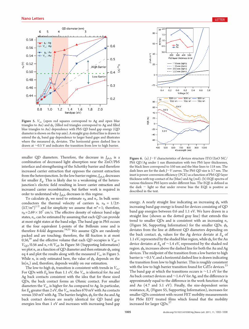
made from the various PbS QD diameters, with Ag (panel a) andAu (panel b) as the back contact. In the Supporting Informationwe show an expanded voltage range as well as the dark J-V
Figure 1. Typical characteristics of J-V in the dark and under 1 sunillumination, which shows the crossover and roll-over effects. The devicestructure is ITO/ZnO NC/PbS QD/Ag with PbS layer thickness of∼550 nm.
Figure 2. (a) Schematic of the inverted solar cell with structure of ITO/ZnO NC/PbS QD/Ag. (b) Two-diode model equivalent circuit includ-ing a heterojunction diode between the ZnO and PbS QD layers and aSchottky junction diode between PbS QD film and Au or Ag. Thejunctions marked by dashed rectangular lines in panel a schematicallyindicate the corresponding diodes in panel b. (c) Device band diagramunder illumination. Holes meet barrier height at the Ag or Au electrode,and electrons can flow in either of two opposite directions to electrode.(See Supporting Information for an SEM imageof a cross sectionof a device.)
1004 dx.doi.org/10.1021/nl103814g |Nano Lett. 2011, 11, 1002–1008
Nano Letters LETTER
curves (Figures S1-S4, Supporting Information). The roll-overeffect is obvious for Eg greater that ∼1 eV and is nearly absentbelow 1 eV. Similarly, the crossover effect is also most pro-nounced for band gaps greater 1 eV and diminishes for smallerband gaps. For small QDs with larger band gap,22 the barrierheight between the PbS layer and Ag is large enough to blockhole-injection; therefore, holes accumulate at the interface,causing the current to saturate. For larger QDs with smallerband gap, the barrier is reduced allowing for some hole injection,which occurs via thermionic emission. The barrier height can alsobe reduced if Au replaces Ag. The J-V characteristics with Au asthe back contact are shown in Figure 3b, because of the lowerwork function the transition from normal J-V curves to onesthat exhibit roll-over and crossover occurs for effective band gapsgreater than∼1.4 eV.While some J-V curves do not exhibit roll-over, almost all exhibit crossover; however, crossover is mostpronounced for the J-V curves that exhibit roll-over. Note thateven for J-V curves that do not exhibit roll-over, the backSchottky junction can limit device performance.23
We model the J-V curves for both Au and Ag back contactdevices using eqs 1-3. The results of a nonlinear least-squaresfitting routine are shown as black dotted lines in Figure 3. Thedark J-V curves were modeled simultaneously with the lightcurves and the dark J-V results are shown in Figures S2 and S4(Supporting Information) as the black dotted lines. The ex-tracted parameters are tabulated in Tables S2 and S3 of theSupporting Information. Previous reports show how the Schott-ky-junction barrier height formed by PbS QD films depends onthe contact work function and QD size.1-4 The current at whichroll-over occurs is determined by the Schottky saturation current,Jso. In Figure 4, we plot the extracted values for Jso and Jph,h as a
function of band gap energy. The extracted photocurrent, Jph,h isthe sum of the photocurrent generated by the heterojunctionminus the photocurrent generated by the Schottky junction,while Jso is related to the Schottky-barrier height by the followingrelationship10
Jso ¼qnvvRe- qφb=kT ð4Þ
where nv is the effective density of valence band states, vR is thethermal velocity of carriers, and φb is the Schottky barrier height.A large Jso indicates a poor Schottky junction. From eq 4, φb isinversely related to Jso. In accordance with our observationsdiscussed above, Jso is high for smaller band gapQDs (larger size)and is lower for higher band gap QDs (smaller size); see Figure 4.For Ag devices, Jso undergoes a transition from high to low at Eg∼ 1.1 eV while for the Au devices the transition occurs at Eg ∼1.4 eV. The blue shaded areas in Figure 4 represent the low-barrier region, and the unshaded areas are the high-barrier region.The extracted photocurrent, Jph,h, exhibits interesting trends andis correlated to the high- or low-barrier regimes. For the highbarrier regime, Jph,h decreases from a maximum at the interfacebetween the high and low barrier regimes as the QD size decreasesand the barrier-height increases. This is likely due to a combinationof increasing photocurrent generated at the Schottky junction thatopposes the main heterojunction current and decreased lightabsorption as the band edge of the QD layer is blue-shifted.Simulations of light absorption10within these types of devices indicatethat light absorbed near the back electrode (within ∼100 nm) isroughly constant with change in QD diameter, while light absor-bed within ∼100 nm of the ZnO/PbS interface decreases for
Figure 3. J-V curves for eight devices made from PbS QDs withvarious diameters. Panel a is for devices with Ag as the back contact andpanel b is for Au. Modeled curves are shown as black dotted lines. Figure 4. Extracted values of the photocurrent (red circles) and
Schottky-barrier saturation current (blue circles) for devices with (a)Ag as back contact and (b) Au.
1005 dx.doi.org/10.1021/nl103814g |Nano Lett. 2011, 11, 1002–1008
Nano Letters LETTER
smaller QD diameters. Therefore, the decrease in Jph,h is acombination of decreased light absorption near the ZnO/PbSinterface and strengthening of the Schottky barrier and thereforeincreased carrier extraction that opposes the current extractionfrom the heterojunction. In the low barrier regime, Jph,h decreasesfor smaller Eg. This is likely due to a weakening of the hetero-junction’s electric field resulting in lower carrier extraction andincreased carrier recombination, but further work is required inorder to understand why Jph,h decreases in this regime.To calculate φb we need to estimate vR and nv. In bulk semi-
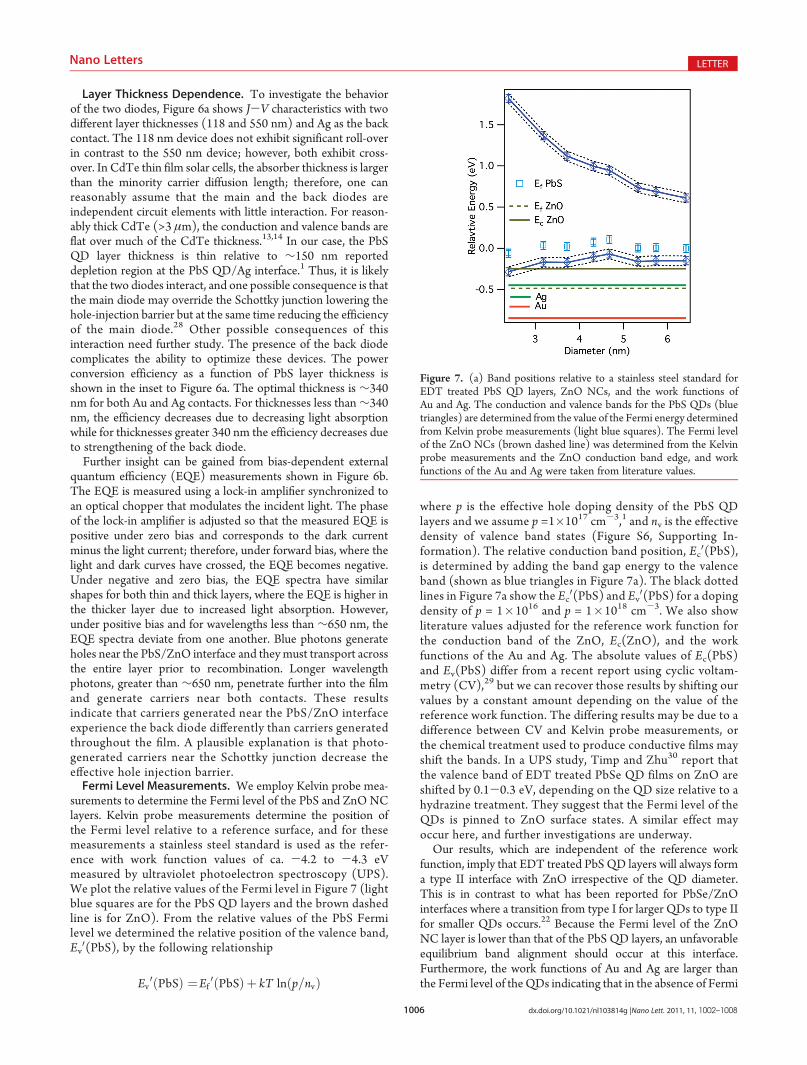
conductors the thermal velocity of carriers is, vR = 1/2π-(kT/m*)1/2 and for simplicity we assume that m*=1; therefore,vR=2.69�107 cm/s. The effective density of valence band edgestates, nv, can be estimated by assuming that each QD can provideat most eight states at the band edge. The band gap in PbS occursat the four equivalent L-points of the Brillouin zone and istherefore 8-fold degenerate.24,25 We assume QDs are randomlypacked and are touching; therefore, the fill fraction is at most0.56,26 and the effective volume that each QD occupies is Veff =VQD/0.56 and nv=8/Veff. In Figure S6 (Supporting Information)we plot nv as a function ofQDdiameter and then estimateφb usingeq 4 and plot the results along with the measured Voc in Figure 5.While nv is only estimated here, the value of φb depends on theln(nv) and, therefore, depends weakly on our estimation.The low-to-high φb transition is consistent with trends in Voc.
For QDs with Eg less than 1.1 eV, the Voc is identical for Au andAg back contacts consistent with the idea that for these sizedQDs, the back contact forms an Ohmic contact. For smallerdiameters the Voc is higher for Au compared to Ag. In particular,for Eg greater than 2 eV, theVoc reaches 670mVwith Au contactsversus 350mVwith Ag. The barrier-heights, φb for the Au and Agback contact devices are nearly identical for QD band gapenergies less than 1 eV and increases with increasing band gap
energy. A nearly straight line indicating an increasing φb withincreasing band gap energy is found for devices consisting of QDband gap energies between 0.6 and 1.1 eV. We have drawn in astraight line (shown as the dotted gray line) that extends thistrend to smaller QDs and is consistent with an increasing nv(Figure S6, Supporting Information) for the smaller QDs. φbdeviates from the line at different QD diameters depending onthe back contact. φb values for the Ag device deviate at Eg of1.1 eV, represented by the shaded blue region, whileφb for the Audevice deviates at Eg of ∼1.4 eV, represented by the shaded redregion. φb increases above the dashed line for both the Au and Agdevices. The midpoint of the transition from a low barrier to highbarrier is∼0.5 V, and a horizontal dashed line is drawn indicatingthe transition from low to high barrier. This is roughly consistentwith the low to high barrier transition found for CdTe devices.23
The band gap at which the transitions occurs is ∼1.1 eV for theAu back contact devices and∼1.4 eV for Ag, and the difference isapproximately equal to the difference in the work function of Agand Au (4.7 and 5.1 eV). Finally, the size-dependent seriesresistance, Rs (Figure S5, Supporting Information), increases forsmaller QDs consistent with recent FET mobility measurementsfor PbSe EDT treated films which found that the mobilityincreased for larger QDs.27
Figure 5. Voc (open red squares correspond to Ag and open bluetriangles to Au) and φb (filled red triangles correspond to Ag and filledblue triangles to Au) dependence with PbS QD band gap energy (QDdiameter is shown on the top axis). A straight gray dotted line is drawn toextend the φb band gap dependence to larger band gaps and illustrateswhere the measured φb deviates. The horizontal green dashed line isdrawn at ∼0.5 V and indicates the transition from low to high barrier.
Figure 6. (a) J-V characteristics of devices structure ITO/ZnO NC/PbS QD/Ag under 1 sun illumination with two PbS layer thicknesses,the black lines correspond to 550 nm and the blue lines to 118 nm. Thedash lines are for the dark J-V curves. The PbS QD size is 3.7 nm. Theinset is power conversion efficiency (PCE) as a function of PbSQD layerthickness with top contact of Au (blue) and Ag (red). (b) EQE spectra ofvarious thickness PbS layers under different bias. The EQE is defined asthe dark - light so that under reverse bias the EQE is positive asdescribed in the text.
1006 dx.doi.org/10.1021/nl103814g |Nano Lett. 2011, 11, 1002–1008
Nano Letters LETTER
Layer Thickness Dependence. To investigate the behaviorof the two diodes, Figure 6a shows J-V characteristics with twodifferent layer thicknesses (118 and 550 nm) and Ag as the backcontact. The 118 nm device does not exhibit significant roll-overin contrast to the 550 nm device; however, both exhibit cross-over. In CdTe thin film solar cells, the absorber thickness is largerthan the minority carrier diffusion length; therefore, one canreasonably assume that the main and the back diodes areindependent circuit elements with little interaction. For reason-ably thick CdTe (>3 μm), the conduction and valence bands areflat over much of the CdTe thickness.13,14 In our case, the PbSQD layer thickness is thin relative to ∼150 nm reporteddepletion region at the PbS QD/Ag interface.1 Thus, it is likelythat the two diodes interact, and one possible consequence is thatthe main diode may override the Schottky junction lowering thehole-injection barrier but at the same time reducing the efficiencyof the main diode.28 Other possible consequences of thisinteraction need further study. The presence of the back diodecomplicates the ability to optimize these devices. The powerconversion efficiency as a function of PbS layer thickness isshown in the inset to Figure 6a. The optimal thickness is ∼340nm for both Au and Ag contacts. For thicknesses less than∼340nm, the efficiency decreases due to decreasing light absorptionwhile for thicknesses greater 340 nm the efficiency decreases dueto strengthening of the back diode.Further insight can be gained from bias-dependent external
quantum efficiency (EQE) measurements shown in Figure 6b.The EQE is measured using a lock-in amplifier synchronized toan optical chopper that modulates the incident light. The phaseof the lock-in amplifier is adjusted so that the measured EQE ispositive under zero bias and corresponds to the dark currentminus the light current; therefore, under forward bias, where thelight and dark curves have crossed, the EQE becomes negative.Under negative and zero bias, the EQE spectra have similarshapes for both thin and thick layers, where the EQE is higher inthe thicker layer due to increased light absorption. However,under positive bias and for wavelengths less than ∼650 nm, theEQE spectra deviate from one another. Blue photons generateholes near the PbS/ZnO interface and theymust transport acrossthe entire layer prior to recombination. Longer wavelengthphotons, greater than ∼650 nm, penetrate further into the filmand generate carriers near both contacts. These resultsindicate that carriers generated near the PbS/ZnO interfaceexperience the back diode differently than carriers generatedthroughout the film. A plausible explanation is that photo-generated carriers near the Schottky junction decrease theeffective hole injection barrier.Fermi Level Measurements. We employ Kelvin probe mea-
surements to determine the Fermi level of the PbS and ZnO NClayers. Kelvin probe measurements determine the position ofthe Fermi level relative to a reference surface, and for thesemeasurements a stainless steel standard is used as the refer-ence with work function values of ca. -4.2 to -4.3 eVmeasured by ultraviolet photoelectron spectroscopy (UPS).We plot the relative values of the Fermi level in Figure 7 (lightblue squares are for the PbS QD layers and the brown dashedline is for ZnO). From the relative values of the PbS Fermilevel we determined the relative position of the valence band,Ev0(PbS), by the following relationship
Ev0ðPbSÞ ¼Ef
0ðPbSÞþ kT lnðp=nvÞ
where p is the effective hole doping density of the PbS QDlayers and we assume p =1�1017 cm-3,1 and nv is the effectivedensity of valence band states (Figure S6, Supporting In-formation). The relative conduction band position, Ec0(PbS),is determined by adding the band gap energy to the valenceband (shown as blue triangles in Figure 7a). The black dottedlines in Figure 7a show the Ec0(PbS) and Ev0(PbS) for a dopingdensity of p = 1�1016 and p = 1�1018 cm-3. We also showliterature values adjusted for the reference work function forthe conduction band of the ZnO, Ec(ZnO), and the workfunctions of the Au and Ag. The absolute values of Ec(PbS)and Ev(PbS) differ from a recent report using cyclic voltam-metry (CV),29 but we can recover those results by shifting ourvalues by a constant amount depending on the value of thereference work function. The differing results may be due to adifference between CV and Kelvin probe measurements, orthe chemical treatment used to produce conductive films mayshift the bands. In a UPS study, Timp and Zhu30 report thatthe valence band of EDT treated PbSe QD films on ZnO areshifted by 0.1-0.3 eV, depending on the QD size relative to ahydrazine treatment. They suggest that the Fermi level of theQDs is pinned to ZnO surface states. A similar effect mayoccur here, and further investigations are underway.Our results, which are independent of the reference work
function, imply that EDT treated PbS QD layers will always forma type II interface with ZnO irrespective of the QD diameter.This is in contrast to what has been reported for PbSe/ZnOinterfaces where a transition from type I for larger QDs to type IIfor smaller QDs occurs.22 Because the Fermi level of the ZnONC layer is lower than that of the PbS QD layers, an unfavorableequilibrium band alignment should occur at this interface.Furthermore, the work functions of Au and Ag are larger thanthe Fermi level of theQDs indicating that in the absence of Fermi
Figure 7. (a) Band positions relative to a stainless steel standard forEDT treated PbS QD layers, ZnO NCs, and the work functions ofAu and Ag. The conduction and valence bands for the PbS QDs (bluetriangles) are determined from the value of the Fermi energy determinedfrom Kelvin probe measurements (light blue squares). The Fermi levelof the ZnO NCs (brown dashed line) was determined from the Kelvinprobe measurements and the ZnO conduction band edge, and workfunctions of the Au and Ag were taken from literature values.
1007 dx.doi.org/10.1021/nl103814g |Nano Lett. 2011, 11, 1002–1008
Nano Letters LETTER
level pinning Au and Ag should form a favorable contact with thePbS layer. However, we have shown evidence for the formationof an unfavorable Schottky barrier with opposite polarity to theheterojunction diode. Therefore, we conclude that the metal/PbS interface undergoes Fermi level pinning, consistent withprevious reports for PbSe QD Schottky junction solar cells.1
The barrier height for a Schottky contact in the absence ofFermi level pinning is determined by the difference in the valenceband edge and the metal Fermi energy (or metal work function).The band bending at the semiconductor-metal interface can becharacterized by the difference in the valence band edge in thebulk layer and at the interface and is related to the barrier height.In the case of Fermi level pinning at the semiconductor/metalinterface, the barrier height is related to the difference betweenthe valence band edge and some characteristic energy level. As Egincreases, the Schottky barrier height increases, consistent withour measurements.The Voc in heterostructure devices is determined by the
difference of the quasi-Fermi level of holes (Efp) at the metal,hole extracting interface, and quasi-Fermi level of electrons (Efn)at the n-type ZnONC/ITO interface.31 Therefore the maximumVoc is determined by the difference in the equilibrium junctionpotential. The realized Voc is determined not only by theenergetics but by the total recombination within the device.Recombination at the interfaces is likely a significant problemwithin this device structure and limits the Voc.The hole-injection barrier can be corrected by two strategies:
the first is to choose a high work function metal such as Au. Ahigh work function contact is required to minimize the hole-injection barrier; however, Fermi level pinning at the QD/metalinterface prevents elimination of the barrier in the structurestested so far.We have shown here that even with a work function that is
larger than the Fermi level of the PbS layer, a Schottky barrier isformed that impedes hole-injection. This is likely due to Fermilevel pinning at the PbS/Au interface. A second strategy invokesthe establishment of a heavily p-doped surface layer in order toenable the tunneling of holes through the barrier height, which isnot easy to achieve in our system but is the subject of futureinvestigations and would lead to better behaved J-V character-istics and corresponding higher conversion efficiencies.In conclusion, the J-V characteristics are investigated in a
heterojunction PbS QD solar cell with structure of ITO/ZnONC/PbS QD/metal and can be described by two opposingdiodes: one formed by the ZnO/PbS interface and the otherby the PbS/metal contact. The Schottky barrier height is afunction of the QD band gap energy and back contact metalwork function. We find that the Fermi levels are pinned at themetal/semiconductor junction and likely at the ZnO NC/PbSQD layer interface as well. Further work to understand andoptimize the interfaces of these hetereosturctured QD solar cellsshould lead to an increase in power conversion efficiency. Therecent demonstration of air stability7 combined with the poten-tial for very high efficiencies32 motivates further investigation ofQD solar cells.
’ASSOCIATED CONTENT
bS Supporting Information. Detailed information on mate-rials, ZnO NCs, PbS QD synthesis, and methods used tofabricate and characterize devices, additional fitting parameters
used to model the J-V curves, and a cross section SEM image ofa typical device structure. This material is available free of chargevia the Internet at http://pubs.acs.org.
’AUTHOR INFORMATION
Corresponding Author*E-mail: [email protected].
’ACKNOWLEDGMENT
The authors thank Mark Hanna, J. C. Johnson, J. van deLagemaat, M. Reese, and A. Nardes for helpful discussions. Wethank Bobby To for SEM imaging. J.G. and R.J.E. were supportedby a PV seed fund provided by the NCPV program at NREL.J.M.L., O.E.S., A.J.N., and M.C.B. were supported by the Centerfor Advanced Photophysics an Energy Frontier Research Centerfunded by U.S. DOE Office of Science. The DOE work wasfunded by Contract DE-AC36-08GO28308 to NREL.
’REFERENCES
(1) Luther, J. M.; Law, M.; Beard, M. C.; Song, Q.; Reese, M. O.;Ellingson, R. J.; Nozik, A. J. Nano Lett. 2008, 8, 3488–3492.
(2) Tang, J.; Wang, X.; Brzozowski, L.; Barkhouse, D. A. R.;Debnath, R.; Levina, L.; Sargent, E. H. Adv. Mater. 2010, 22, 1–5.
(3) Johnston, K. W.; Pattantyus-Abraham, A. G.; Clifford, J. P.;Myrskog, S. H.; Hoogland, S.; Shukla, H.; Klem, E. J. D.; Sargent, E. H.Appl. Phys. Lett. 2008, 92, No. 122111.
(4) Tang, J.; Brzozowski, L.; Barkhouse, D. A. R.; Wang, X.;Debnath, R.; Wolowiec, R.; Palmiano, E.; Levina, L.; Pattantyus-Abraham, A. G.; Jamakosmanovic, D.; Sargent, E. H. ACS Nano 2010,4, 869–878.
(5) Choi, J. J.; Lim, Y.; Santiago-Berrios, M. B.; Oh, M.; Hyun, B.;Sun, L.; Bartnik, A. C.; Goedhart, A.; Malliaras, G. G.; Abru~na, H. D.;Wise, F. W.; Hanrath, T. Nano Lett. 2009, 9, 3749–3755.
(6) Leschkies, K. S.; Beatty, T. J.; Kang, M. S.; Norris, D. J.; Aydil,E. S. ACS Nano 2009, 3, 3638–3648.
(7) Luther, J. M.; Gao, J.; Lloyd,M. T.; Semonin, O. E.; Beard,M. C.;Nozik, A. J. Adv. Mater. 2010, 22, 3704–3707.
(8) Pattantyus-Abraham, A. G.; Kramer, I. J.; Barkhouse, A. R.;Wang, X.; Konstantatos, G.; Debnath, R.; Levina, L.; Raabe, I.;Nazeeruddin, M. K.; Gr€atzel, M.; Sargent, E. H. ACS Nano 2010, 4,3374–3380.
(9) Ma, W.; Luther, J. M.; Zheng, H.; Wu, Y.; Alivisatos, A. P. NanoLett. 2009, 9, 1699–1703.
(10) Law, M.; Beard, M. C.; Choi, S.; Luther, J. M.; Hanna, M. C.;Nozik, A. J. Nano Lett. 2008, 11, 3904–3910.
(11) Demtsu, S. H.; Sites, J. R. Thin Solid Films 2006, 510, 320–324.(12) Niemegeers, A.; Burgelman, M. J. Appl. Phys. 1997, 81, 2881–
2886.(13) Godoy, A.; Cattin, L.; Toumi, L.; Diaz, F. R.; del Valle, M. A.;
Soto, G. M.; Kouskoussa, B.; Morsli, M.; Benchouk, K.; Khelil, A.;Bernede, J. C. Sol. Energy Mater. Sol. Cells 2010, 94, 648–654.
(14) Kouskoussa, B.; Morsli, M.; Benchouk, K.; Louarn, G.; Cattin,L.; Khelil, A.; Bern�ede, J. C. Phys. Status Solidi A 2009, 206, 311–315.
(15) Gill, W. D.; Bube, R. H. J. Appl. Phys. 1970, 41, 3731.(16) Pfisterer, F. Thin Solid Films 2003, 431, 470.(17) Rothwarf, A. Sol. Cells 1980, 2, 115.(18) Green, M. A. Solar Cells: Operating Principles, Technology, and
System Applications; Prentice-Hall: Englewood Cliffs, NJ, 1982.(19) Wu, Y.; Wadia, C.; Ma, W.; Sadtler, B.; Alivisatos, A. P. Nano
Lett. 2008, 8, 2551–2555.(20) Jain, A.; Kapoor, A. Sol. Energy Mater. Sol. Cells 2005, 86, 197–
205.(21) Mazhari, B. Sol. Energy Mater. Sol. Cells 2006, 90, 1021–1033.
1008 dx.doi.org/10.1021/nl103814g |Nano Lett. 2011, 11, 1002–1008
Nano Letters LETTER
(22) Hyun, B. -B; Zhong, Y-W; Bartnik, A. C.; Sun, L.; Abru~na,H. D.; Wise, F. W.; Goodreau, J. D.; Matthews, J. R.; Leslie, T. M.;Borrelli, N. F. ACS Nano 2008, 11, 2206–2212.(23) Pan, J; Gloeckler, M.; Sites, J. R. J. Appl. Phys. 2006, 100,
124505.(24) Kang, I.; Wise, F. W. J. Opt. Soc. Am. B 1997, 14, 1632–1646.(25) Wehrenberg, B. L.; Yu, D.; Ma, J.; Guyot-Sionnest, P. J. Phys.
Chem. B 2005, 109, 20192–20199.(26) Luther, J. M.; Law, M.; Song, Q.; Perkins, C. L.; Beard, M. C.;
Nozik, A. J. ACS Nano 2008, 2, 271–280.(27) Liu, Y.; Gibbs, M.; Puthussery, J.; Gaik, S.; Ihly, R.; Hillhouse,
H. W.; Law, M. Nano Lett. 2010, 10, 1960–1969.(28) Sze, S. Physics of Semiconductor Devices, 2nd ed.; Wiley:
New York, 1981.(29) Hyun, B.-R.; Zhong, Y.-W.; Bartnik, A. C.; Sun, L.; Abruna,
H. D.; Wise, F. W.; Goodreau, J. D.; Matthews, J. R.; Leslie, T. M.;Borrelli, N. F. ACS Nano 2008, 2, 2206–2212.(30) Timp, B. A.; Zhu, X. Y. Surf. Sci. 2010, 604, 1335–1341.(31) Gregg, B. A.; Hanna, M. C. J. Appl. Phys. 2003, 93, 3605–3614.(32) Beard, M. C.; Midgett, A. G.; Hanna, M. C.; Luther, J. M.;
Hughes, B. K.; Nozik, A. J. Nano Lett. 2010, 10, 3019–3027.

![Zur Elektrodynamik bewegter Körper [AdP 17, 891 (1905)]astro1.panet.utoledo.edu/~ljc/bewegter_k.pdf · Title: Zur Elektrodynamik bewegter Körper [AdP 17, 891 (1905)] Author: Katharina](https://img.pdfslide.tips/doc/110x75/6071e650e59c0d1376292346/zur-elektrodynamik-bewegter-krper-adp-17-891-1905-ljcbewegterkpdf-title.jpg)