Embed Size (px)
Citation preview

Acta Materialia 197 (2020) 212–223
Contents lists available at ScienceDirect
Acta Materialia
journal homepage: www.elsevier.com/locate/actamat
Full length article
Superconducting Cu/Nb nanolaminate by coded accumulative roll
bonding and its helium damage characteristics
Rui Gao
a , b , Miaomiao Jin
b , c , ∗, Fei Han
b , Baoming Wang
d , Xianping Wang
a , ∗, Qianfeng Fang
a , Yanhao Dong
a , Cheng Sun
e , Lin Shao
f , Mingda Li b , Ju Li b , d , ∗
a Key Laboratory of Materials Physics, Institute of Solid State Physics, Chinese Academy of Sciences, Hefei 230031, PR China b Department of Nuclear Science and Engineering, Massachusetts Institute of Technology, Cambridge, MA 02139, United States c Department of Fuels Modeling and Simulation, Idaho National Laboratory, Idaho Falls, ID 83415, USA d Department of Materials Science and Engineering, Massachusetts Institute of Technology, Cambridge, MA 02139, United States e Characterization and Advanced PIE Division, Idaho National Laboratory, Idaho Falls, ID 83415, USA f Department of Nuclear Engineering, Texas A&M University, College Station, TX 77845, USA
a r t i c l e i n f o
Article history:
Received 22 April 2020
Revised 9 July 2020
Accepted 10 July 2020
Available online 15 July 2020
Keywords:
Hierarchical nanolaminates
Superconductor
Helium irradiation resistance
Mechanical properties
Accumulative roll bonding
a b s t r a c t
A very broad distribution of microstructural length scales spanning few nm- to the μm-scale has proven
effective to achieve exceptional materials properties. Here, we fabricate a Cu/Nb two-phase composite
made of a hierarchically layered structure by modifying the conventional accumulative roll bonding (ARB)
technique, where fresh Nb sheets are inserted and bonded during a repeated stacking and rolling process.
This barcode-like multilayer with a designed hierarchical length scale distribution possesses densely dis-
tributed phase boundaries and rich interfacial structures. The composite demonstrates similar supercon-
ductivity characteristics as pure Nb, but is 3 × stronger, has theoretically better oxidation resistance, and
retains considerable ductility. Under the helium irradiation environment, the unique interfacial structures
featuring chemical intermixing zones (3-dimensional) are more immune to the formation of large helium
clusters than atomically sharp interfaces (2-dimensional), screening them from radiation damage and im-
proving their long-term mechanical integrity. This work signifies an effective strategy of constructing hi-
erarchical laminates to achieve high-performance materials, which holds promise in fusion and fission
energy applications.
© 2020 Published by Elsevier Ltd on behalf of Acta Materialia Inc.
1. Introduction
Manipulating microstructural length scales is a well-utilized de-
sign strategy to optimize materials properties, such as the trade-off
between strength and ductility of metallic alloys [1] . Severe plastic
deformation (SPD) including equal channel angular pressing (ECAP)
[2] , high-pressure torsion (HPT) [3] and accumulative roll bond-
ing (ARB) [4] , can be used to refine grains and/or introduce lay-
ered structures to improve the strength of materials. In contrast
to the unimodal grain sizes or multilayer spacing, recent studies
demonstrated that a judicious combination of multiple character-
istic dimensions in a material spanning from the nanoscale to the
macroscale could be more effective to obtain a better-integrated
behavior than a unimodal nanoscaled material [5 , 6] . For example,
Ma and coworkers [7] reported a high ductility in a nanostructured
∗ Corresponding authors.
E-mail addresses: [email protected] (M. Jin), [email protected] (X. Wang),
[email protected] (J. Li).
Cu with a bimodal grain size distribution prepared by cold rolling
and proper heat treatments, as the coarse microstructure sustains
strain-hardening to stabilize tensile deformation while the fine
part imparts strength. Lu [8] demonstrated a gradient microstruc-
ture introduced by surface mechanical attrition treatment with a
variety of grain sizes, leading to a good strength-ductility tradeoff.
Another example is multilayered structures where the ductility of
cold-rolled Cu/Cu laminates nearly doubles that of cold-rolled Cu
alone due to decreased necking facilitated by the laminated struc-
ture with a broad range of layer thicknesses ranging from 1.8 μm
- 500 nm [9] .
However, multi-scale materials with a certain portion of nano-
sized grains could be unstable when exposed to extreme condi-
tions encountered in nuclear fission or fusion, because smaller
grain sizes contribute to a high driving force for recrystallization
and/or abnormal grain growth under irradiation and thermal envi-
ronment [10 , 11] . A single-phase structure can easily coarsen due to
the high mobility of grain boundaries (GBs) via short-range diffu-
sion, which degrades the long-term mechanical properties. To over-
https://doi.org/10.1016/j.actamat.2020.07.031
1359-6454/© 2020 Published by Elsevier Ltd on behalf of Acta Materialia Inc.
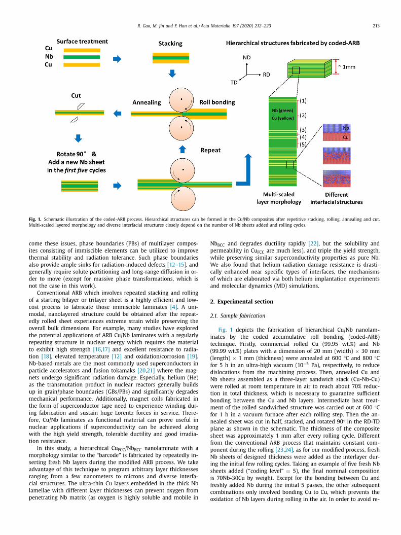
R. Gao, M. Jin and F. Han et al. / Acta Materialia 197 (2020) 212–223 213
Fig. 1. Schematic illustration of the coded-ARB process. Hierarchical structures can be formed in the Cu/Nb composites after repetitive stacking, rolling, annealing and cut.
Multi-scaled layered morphology and diverse interfacial structures closely depend on the number of Nb sheets added and rolling cycles.
come these issues, phase boundaries (PBs) of multilayer compos-
ites consisting of immiscible elements can be utilized to improve
thermal stability and radiation tolerance. Such phase boundaries
also provide ample sinks for radiation-induced defects [12–15] , and
generally require solute partitioning and long-range diffusion in or-
der to move (except for massive phase transformations, which is
not the case in this work).
Conventional ARB which involves repeated stacking and rolling
of a starting bilayer or trilayer sheet is a highly efficient and low-
cost process to fabricate those immiscible laminates [4] . A uni-
modal, nanolayered structure could be obtained after the repeat-
edly rolled sheet experiences extreme strain while preserving the
overall bulk dimensions. For example, many studies have explored
the potential applications of ARB Cu/Nb laminates with a regularly
repeating structure in nuclear energy which requires the material
to exhibit high strength [16 , 17] and excellent resistance to radia-
tion [18] , elevated temperature [12] and oxidation/corrosion [19] .
Nb-based metals are the most commonly used superconductors in
particle accelerators and fusion tokamaks [20 , 21] where the mag-
nets undergo significant radiation damage. Especially, helium (He)
as the transmutation product in nuclear reactors generally builds
up in grain/phase boundaries (GBs/PBs) and significantly degrades
mechanical performance. Additionally, magnet coils fabricated in
the form of superconductor tape need to experience winding dur-
ing fabrication and sustain huge Lorentz forces in service. There-
fore, Cu/Nb laminates as functional material can prove useful in
nuclear applications if superconductivity can be achieved along
with the high yield strength, tolerable ductility and good irradia-
tion resistance.
In this study, a hierarchical Cu FCC /Nb BCC nanolaminate with a
morphology similar to the “barcode” is fabricated by repeatedly in-
serting fresh Nb layers during the modified ARB process. We take
advantage of this technique to program arbitrary layer thicknesses
ranging from a few nanometers to microns and diverse interfa-
cial structures. The ultra-thin Cu layers embedded in the thick Nb
lamellae with different layer thicknesses can prevent oxygen from
penetrating Nb matrix (as oxygen is highly soluble and mobile in
Nb BCC and degrades ductility rapidly [22] , but the solubility and
permeability in Cu FCC are much less), and triple the yield strength,
while preserving similar superconductivity properties as pure Nb.
We also found that helium radiation damage resistance is drasti-
cally enhanced near specific types of interfaces, the mechanisms
of which are elaborated via both helium implantation experiments
and molecular dynamics (MD) simulations.
2. Experimental section
2.1. Sample fabrication
Fig. 1 depicts the fabrication of hierarchical Cu/Nb nanolam-
inates by the coded accumulative roll bonding (coded-ARB)
technique. Firstly, commercial rolled Cu (99.95 wt.%) and Nb
(99.99 wt.%) plates with a dimension of 20 mm (width) × 30 mm
(length) × 1 mm (thickness) were annealed at 600 °C and 800 °C
for 5 h in an ultra-high vacuum (10 −5 Pa), respectively, to reduce
dislocations from the machining process. Then, annealed Cu and
Nb sheets assembled as a three-layer sandwich stack (Cu-Nb-Cu)
were rolled at room temperature in air to reach about 70% reduc-
tion in total thickness, which is necessary to guarantee sufficient
bonding between the Cu and Nb layers. Intermediate heat treat-
ment of the rolled sandwiched structure was carried out at 600 °C
for 1 h in a vacuum furnace after each rolling step. Then the an-
nealed sheet was cut in half, stacked, and rotated 90 ° in the RD-TD
plane as shown in the schematic. The thickness of the composite
sheet was approximately 1 mm after every rolling cycle. Different
from the conventional ARB process that maintains constant com-
ponent during the rolling [23 , 24] , as for our modified process, fresh
Nb sheets of designed thickness were added as the interlayer dur-
ing the initial few rolling cycles. Taking an example of five fresh Nb
sheets added (“coding level” = 5), the final nominal composition
is 70Nb-30Cu by weight. Except for the bonding between Cu and
freshly added Nb during the initial 5 passes, the other subsequent
combinations only involved bonding Cu to Cu, which prevents the
oxidation of Nb layers during rolling in the air. In order to avoid re-

214 R. Gao, M. Jin and F. Han et al. / Acta Materialia 197 (2020) 212–223
Table 1
As for Cu/Nb multilayers with the component of 70 wt% Nb and 30 wt% Cu, the nominal thickness
of the multi-scaled layers with the number of rolling cycles.
Rolling cycles Nominal thickness of the multi-scaled layers (nm) 70 wt% Nb–30 wt% Cu
Cu Nb (1) Nb (2) Nb (3) Nb (4) Nb (5)
15 4 4 12 36 109 326
13 16 16 48 145 434 1302
11 64 64 193 579 1736 5208
9 257 257 772 2315 6944 20,833
7 1029 1029 3086 9259 27,778 83,333
arrangement of the interfacial atomic structures, the thermal treat-
ment was not applied during the last three rolling cycles.
In this paper, all the characterization focused on the 70Nb-
30Cu by weight nanolaminate after 15 rolling cycles unless other-
wise specified. The nominal individual layer thicknesses were cal-
culated assuming the equal thickness reduction rate in Nb and
Cu layers during coded-ARB ( Table 1 ). The layered morphology
of Cu/Nb laminates was studied by scanning electron microscope
(SEM, Sirion200, FEI, USA) combined with energy-dispersive X-ray
spectroscopy (EDS).
2.2. Mechanical property and superconductivity characterization of
Cu/Nb nano-multilayer composites
The strength and ductility of hierarchical Cu/Nb laminates
at room temperature were examined by uniaxial tensile test-
ing. The dogbone tensile specimens with gauge dimensions
5 mm × 1.5 mm × 0.75 mm were cut from the RD-TD plane in
each bulk composite at different rolling cycles by electrical dis-
charge machining. Such specimens maintain structural integrity af-
ter the cutting and subsequent mechanical polishing. Tensile tests
were carried out parallel to the RD of samples using an Instron
3369 Dual Column Tabletop Testing System with a constant dis-
placement rate of 0.1 mm/min. The displacement of tensile sam-
ples was measured by a strain gauge type extensometer. Every
strain-stress curve is derived from the average of three replicate
tests. Experimental details of the tensile test are described in the
Supplementary Information.
The electrical resistivity at room temperature of initial annealed
Cu and Nb plates are 2.26 × 10 −8 � · m and 2.02 × 10 −7 � · m,
respectively. All the Cu/Nb samples for resistivity measurement
are prepared with a size of 10 mm × 3 mm × 0.1 mm. Impor-
tantly, such tapes were annealed at 350 °C for 2 h in an ultra-
high vacuum to relieve residual stress after mechanical polish-
ing. The sample preparation method is elaborated in the Supple-
mentary Information. The superconducting transition resistivity of
pure Nb and Cu/Nb films was analyzed according to the resistance
test that was performed with an AC bridge using the conventional
four-probe method in the physical property measurement system
(PPMs). These tests were carried out in a helium cryostat equipped
with a superconducting solenoid providing fields up to 1.5 Tesla.
The temperature was controlled in the range of 2–12 K with an
accuracy of ±1 mK. And the plane of rolling-normal directions of
samples was perpendicular to the magnetic field. T c was defined
as the midpoints of the resistive transitions R ( T ) .
2.3. He ion implantation and post-irradiation examination
Bulk Cu/Nb laminates without annealing were subjected to
300 keV He ion irradiation with two fluences of 1 × 10 17 ions/cm
2
and 5 × 10 17 ions/cm
2 by using a 400 kV accelerator at Texas A&M
University, which were noted as lower and higher dose irradia-
tion in this paper, respectively. The irradiation was performed at
room temperature with an accuracy of ±10 °C. Helium concentra-
tion (4.2 at% and 21 at%, low and high dose, respectively) as a func-
tion of irradiation depth (~830 nm) is estimated by SRIM (Stop-
ping and Range of Ions in Solids) software. The average thresh-
old displacement energy of 29 eV for Cu and 41 eV for Nb are
applied in the calculation, respectively. To investigate the evolu-
tion of interfacial structures and bubbles morphology during the
irradiation, cross-sectional transmission electron microscope (TEM)
lamellae were prepared by the lift-out technique using the FEI He-
lios Nanolab 600 Dual Beam System (FIB) at 30 kV followed by low
energy cleaning at 2 kV. The microstructure was characterized us-
ing a JEOL 2010F TEM operated at 200 kV.
2.4. Molecular dynamics simulation of radiation damage and helium
bubble formation
MD simulations with the LAMMPS package [25] are used to
examine Cu/Nb interfacial evolution under helium irradiation. The
atomic interactions are described by an EAM potential [26] , which
is smoothly joined to the ZBL potential [27] to accommodate
high energy atomic collisions. We constructed three bi-crystal sys-
tems containing three types of interfaces. The orientation of Cu
and Nb layers marked in Fig. 8 is consistent with the experi-
mental observations, and the thickness of each layer is 10 nm.
The configurations contain 235,926 atoms, with a dimension of
13.4 nm × 12.6 nm × 20 nm and periodic boundary conditions.
Based on the sharp interface system, the interfacial transition zone
(ITZ) is created by randomly mixing Cu and Nb atoms within the
2 nm thickness interfacial domains. To generate the amorphous in-
terfaces, the following procedure is utilized: i) the 2 nm slabs are
melted at 1600 K for 200 ps with the rest of the atoms fixed, grad-
ually quenched to 650 K over a span of 200 ps, ii) the whole sys-
tem is quenched from 650 K to 300 K over 200 ps; iii) the whole
system is first relaxed at zero pressure for 30 ps, and then at con-
stant volume for another 30 ps. Finally, the three types of configu-
rations are prepared for the helium radiation study.
To mimic the radiation process, we applied a multi-cascade
molecular dynamics (MD) simulation algorithm [28] . Specifically,
random cascades induced by 5 keV primary knock-on atoms (PKAs)
are sequentially introduced into the simulation box, and each cas-
cade lasts around 30 ps until the system is adequately annealed
to ambient temperature. The ambient environment is modeled by
thermostating the box boundary at 300 K, so that the excess en-
ergy from the PKAs gets drained gradually from the MD supercell.
The radiation damage can be estimated with the NRT formulation
[29] , and one can obtain the experimental dose level by increas-
ing the number of PKAs with additional computational cost. To
account for helium atoms implantation at around the experimen-
tal helium/dpa ratio, on average, two He atoms are randomly cre-
ated in the simulation box along with each PKA, and this accumu-
lated helium evolves naturally upon damage cascades. The evolving
atomic configurations are used for tracking helium behavior. The
visualization is performed with the OVITO package [30] .

R. Gao, M. Jin and F. Han et al. / Acta Materialia 197 (2020) 212–223 215
Fig. 2. The cross-sectional SEM images (a–c) and EDS mapping (a1–c1) of Cu/Nb multilayers with different components under the same rolling cycles. Different “barcode”
structures, especially with highly variable Nb layer thicknesses, can be manipulated by the coded-ARB technique (a and b), compared to the homogeneous layered structure
with nearly equal thickness prepared by traditional ARB (c). Scale bars in (a–c) are 100 μm and (a1–c1) are 200 μm, respectively.
3. Results
3.1. Microstructure characterization
3.1.1. Multi-scale layered morphology
As the Cu and Nb layers must undergo the same areal expan-
sion to avoid delamination or rupture during rolling, and as plas-
tic deformation conserves volume, the thickness ratio of all lay-
ers is preserved before and after rolling (assuming no mechan-
ically driven intermixing). Thus, our only chances to modify the
thickness distribution and phase fraction are by inserting fresh Nb
layer of certain thickness after stacking and before roll-bonding
step. How much fresh Nb we choose to insert each time is the
“coding” part of coded-ARB. On one hand, the programed inser-
tion or “code” controls the local stress/strain field inside the bulk
to maintain layer integrity (detailed in the discussion section), and
on the other hand, it can produce hierarchical structures to opti-
mize properties.
Fig. 2 compares the secondary electron-SEM images (a–c) and
EDS mapping (a1–c1) of layer morphology of Cu/Nb multilayers
after the same 7 rolling cycles using current manufacturing strat-
egy and conventional ARB. When inserting seven and four fresh
Nb sheets during the coded-ARB process ( Fig. 2 a and b), the layer
morphology becomes similar to “barcodes”. It demonstrates that
“barcode” structures, especially with highly variable Nb layer thick-
nesses taken up at different “coding levels”, can be manipulated
with the coded-ARB technique, compared to a homogeneous lay-
ered structure with nearly equal thickness prepared by traditional
ARB ( Fig. 2 c). From these images, the interfaces are wavy and the
layers remain continuous without fracture. Nb itself is very ductile
in an oxygen-free environment, but can strain-harden significantly
and quickly become brittle in the presence of oxygen [22] . How-
ever, the Cu layers can reduce oxygen permeation during rolling,
so that even our nanoscale Nb layers maintain excellent deforma-
bility ( Fig. 3 a). Element distribution maps as shown in Fig. 2 a 1 and
b1 demonstrate the multi-scale, heterogeneous structures in these
composites with highly varying Nb layer thicknesses as different
numbers of Nb sheets are added (see supplementary Table S1 for
the distribution of nominal layer thickness). Moreover, diverse bar-
code structures can be also controlled by changing rolling cycles
when the composition is fixed (see Supplementary Fig. S1).
After 15 rolling cycles ( Fig. 3 a), the thicknesses of both Cu phase
and Nb phase can be reduced to the nanoscale. The nanoscaled
“barcode” layered structure we obtained is uniform (see Fig. 3 a),
meaning that the layer thickness is almost constant at different
in-plane locations with minimal deviation, hence, we performed
a single measurement for the thickness of each layer in the direc-
tion perpendicular to the interfaces. Two TEM foils were lift-out
at a depth of about 7 μm and 15 μm from the polished surface
by focused ion beam (FIB), respectively, and for each foil, five TEM
images with a magnification of 30,0 0 0 were captured with an or-
der from top to bottom. The total measurements we have done to
get the distribution of the layer thickness is around 800, i.e. from
800 different layers. The distribution statistics of Cu and Nb lay-
ers thickness is shown in Fig. 3 b. About 57% of layers drop below
10 nm thick, while only 6% of layers are more than 100 nm thick.
The fraction of layers distributed within 10–50 nm, 50–100 nm is
22% and 15%, respectively. Almost all the Cu layers are less than
10 nm thick. In addition, although the number of thick Nb layers
is small, the total thickness of such layers whose thickness exceeds
100 nm occupies at least 100 μm in a 1mm-thick sample, illustrat-
ing the fractal-like morphology of our samples.
3.1.2. Diverse interfacial structures
In the case of highly variable layer thickness, interfacial struc-
tures become complex due to the shear instability driven by de-
formation and layer incompatibility, say, occurring between a very
thin Cu layer and a very thick Nb layer. Here we distinguish three
types of interfaces based on their atomic structures: atomically
sharp interface, interfacial transition zone (ITZ), and amorphous
zone (AMO). It has been observed that a large fraction of inter-
faces are relatively straight at a low magnification. As indicated in
high-resolution images ( Fig. 3 d), some interfaces with well-defined
lattice orientation relationships (OR) are atomically sharp due to
the immiscible nature between neighboring Cu and Nb phases. Ir-
regular zones representing chemical intermixing interfaces are in-
dicated in Fig. 3 e, where they look smeared and usually appear
on either side of an ultra-thin layer with thicknesses less than
10 nm. And an FFT image obtained from a HRTEM image of this
Nb layer was inserted. Fig. 3 f shows a HRTEM image of interfaces
with the crystallographic orientation relationship (OR) [112] Cu ||
[110] Nb . At the sharp interface plane, the close-packed planes of
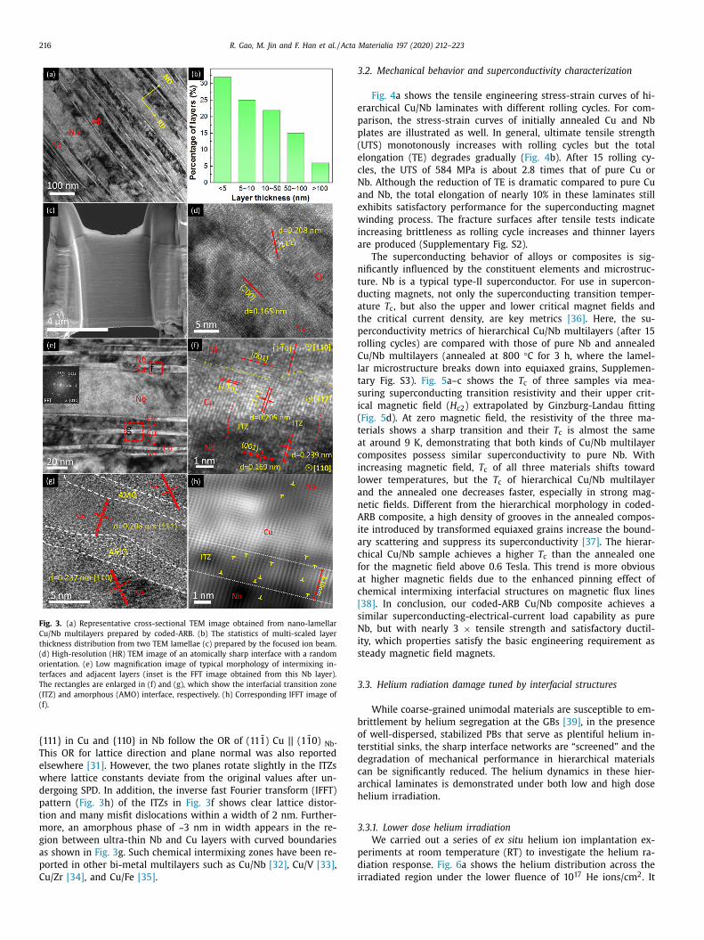
216 R. Gao, M. Jin and F. Han et al. / Acta Materialia 197 (2020) 212–223
Fig. 3. (a) Representative cross-sectional TEM image obtained from nano-lamellar
Cu/Nb multilayers prepared by coded-ARB. (b) The statistics of multi-scaled layer
thickness distribution from two TEM lamellae (c) prepared by the focused ion beam.
(d) High-resolution (HR) TEM image of an atomically sharp interface with a random
orientation. (e) Low magnification image of typical morphology of intermixing in-
terfaces and adjacent layers (inset is the FFT image obtained from this Nb layer).
The rectangles are enlarged in (f) and (g), which show the interfacial transition zone
(ITZ) and amorphous (AMO) interface, respectively. (h) Corresponding IFFT image of
(f).
{111} in Cu and {110} in Nb follow the OR of (11 ̄1 ) Cu || (1 ̄1 0) Nb .
This OR for lattice direction and plane normal was also reported
elsewhere [31] . However, the two planes rotate slightly in the ITZs
where lattice constants deviate from the original values after un-
dergoing SPD. In addition, the inverse fast Fourier transform (IFFT)
pattern ( Fig. 3 h) of the ITZs in Fig. 3 f shows clear lattice distor-
tion and many misfit dislocations within a width of 2 nm. Further-
more, an amorphous phase of ~3 nm in width appears in the re-
gion between ultra-thin Nb and Cu layers with curved boundaries
as shown in Fig. 3 g. Such chemical intermixing zones have been re-
ported in other bi-metal multilayers such as Cu/Nb [32] , Cu/V [33] ,
Cu/Zr [34] , and Cu/Fe [35] .
3.2. Mechanical behavior and superconductivity characterization
Fig. 4 a shows the tensile engineering stress-strain curves of hi-
erarchical Cu/Nb laminates with different rolling cycles. For com-
parison, the stress-strain curves of initially annealed Cu and Nb
plates are illustrated as well. In general, ultimate tensile strength
(UTS) monotonously increases with rolling cycles but the total
elongation (TE) degrades gradually ( Fig. 4 b). After 15 rolling cy-
cles, the UTS of 584 MPa is about 2.8 times that of pure Cu or
Nb. Although the reduction of TE is dramatic compared to pure Cu
and Nb, the total elongation of nearly 10% in these laminates still
exhibits satisfactory performance for the superconducting magnet
winding process. The fracture surfaces after tensile tests indicate
increasing brittleness as rolling cycle increases and thinner layers
are produced (Supplementary Fig. S2).
The superconducting behavior of alloys or composites is sig-
nificantly influenced by the constituent elements and microstruc-
ture. Nb is a typical type-II superconductor. For use in supercon-
ducting magnets, not only the superconducting transition temper-
ature T c , but also the upper and lower critical magnet fields and
the critical current density, are key metrics [36] . Here, the su-
perconductivity metrics of hierarchical Cu/Nb multilayers (after 15
rolling cycles) are compared with those of pure Nb and annealed
Cu/Nb multilayers (annealed at 800 °C for 3 h, where the lamel-
lar microstructure breaks down into equiaxed grains, Supplemen-
tary Fig. S3). Fig. 5 a–c shows the T c of three samples via mea-
suring superconducting transition resistivity and their upper crit-
ical magnetic field ( H c2 ) extrapolated by Ginzburg-Landau fitting
( Fig. 5 d). At zero magnetic field, the resistivity of the three ma-
terials shows a sharp transition and their T c is almost the same
at around 9 K, demonstrating that both kinds of Cu/Nb multilayer
composites possess similar superconductivity to pure Nb. With
increasing magnetic field, T c of all three materials shifts toward
lower temperatures, but the T c of hierarchical Cu/Nb multilayer
and the annealed one decreases faster, especially in strong mag-
netic fields. Different from the hierarchical morphology in coded-
ARB composite, a high density of grooves in the annealed compos-
ite introduced by transformed equiaxed grains increase the bound-
ary scattering and suppress its superconductivity [37] . The hierar-
chical Cu/Nb sample achieves a higher T c than the annealed one
for the magnetic field above 0.6 Tesla. This trend is more obvious
at higher magnetic fields due to the enhanced pinning effect of
chemical intermixing interfacial structures on magnetic flux lines
[38] . In conclusion, our coded-ARB Cu/Nb composite achieves a
similar superconducting-electrical-current load capability as pure
Nb, but with nearly 3 × tensile strength and satisfactory ductil-
ity, which properties satisfy the basic engineering requirement as
steady magnetic field magnets.
3.3. Helium radiation damage tuned by interfacial structures
While coarse-grained unimodal materials are susceptible to em-
brittlement by helium segregation at the GBs [39] , in the presence
of well-dispersed, stabilized PBs that serve as plentiful helium in-
terstitial sinks, the sharp interface networks are “screened” and the
degradation of mechanical performance in hierarchical materials
can be significantly reduced. The helium dynamics in these hier-
archical laminates is demonstrated under both low and high dose
helium irradiation.
3.3.1. Lower dose helium irradiation
We carried out a series of ex situ helium ion implantation ex-
periments at room temperature (RT) to investigate the helium ra-
diation response. Fig. 6 a shows the helium distribution across the
irradiated region under the lower fluence of 10 17 He ions/cm
2 . It

R. Gao, M. Jin and F. Han et al. / Acta Materialia 197 (2020) 212–223 217
Fig. 4. (a)Tensile engineering stress-strain curves for the bulk pure Cu, pure Nb, and coded-ARB Cu/Nb nanolaminates with different rolling cycles. (b) The ultimate tensile
strength (UTS) and tensile elongation (TE) of the pure Cu, pure Nb and coded-ARB Cu/Nb nanolaminates with different rolling cycles, respectively.
Fig. 5. Resistivity superconducting transitions of (a) hierarchical Cu/Nb multilayers, (b) annealed Cu/Nb multilayers, and (c) pure Nb at different magnetic fields. (d) Phase
diagram of the critical field derived from the resistivity transition curves. The superconducting transition temperatures ( T c ) of hierarchical Cu/Nb multilayers (black), an-
nealed Cu/Nb multilayers (red), and pure Nb (blue) are presented as solid circles. The solid line shows the theoretical curve fit based on the Ginzburg-Landau theory. (For
interpretation of the references to color in this figure legend, the reader is referred to the web version of this article.)
can be seen that a large number of tiny bubbles exist within 500–
800 nm from the surface. The peak helium concentration is about
4 at% according to the SRIM (Stopping and Range of Ions in Solids)
calculation [40] . Except for some bubbles as bright white spots
preferentially located in the Cu layers ( Fig. 6 b), other ones also reg-
ularly align as spindle-shaped channels at the sharp interface as
shown in Fig. 6 c, demonstrating a phase-boundary wetting char-
acteristic [41 , 42] . In contrast, helium precipitates distributed in the
intermixing regions are more isolated, exhibiting no helium bubble
alignment. Fig. 6 d illustrates that some separate bubbles with a di-
ameter of ~0.7 nm are embedded fully inside the Cu layer near the
amorphous zone, but bubbles are hardly observed by HRTEM in
the amorphous zone or near crystalline-amorphous interface from
the Nb side (denoted as the bubble denuded zone, or BDZ). Fig. 6 e

218 R. Gao, M. Jin and F. Han et al. / Acta Materialia 197 (2020) 212–223
Fig. 6. Under a He irradiation dose of 10 17 ions/cm
2 , (a) a typical cross-section TEM image showing the distribution of irradiation-induced bubbles within the helium
implanted region. (b) Local enlarged region of the concentrated He bubbles, corresponding to the area marked with a red square in (a). HRTEM images of He bubble
morphology in (c) sharp interfaces and interfacial transition zones, and (d) the amorphous area. (e) Schematic of helium bubble evolution as the function of interfacial
structures according to the experimental observation, where BDZ stands for bubble denuded zone. (For interpretation of the references to color in this figure, the reader is
referred to the web version of this article.)
schematically shows the evolution of helium bubbles at the three
types of interfaces. ITZ and amorphous interfaces hinder the for-
mation of large bubbles even under this extremely large dose of
helium implantation (40,0 0 0 appm, one or two orders of magni-
tude larger than fusion vacuum vessel conditions at end of life)
[43] , in contrast to the sharp interfaces where helium bubble pro-
duction is preferable. It is worth mentioning that the amorphous
nature of these interfaces is still maintained after irradiation.
3.3.2. Higher dose helium irradiation
Fig. 7 a indicates the microstructure of hierarchical Cu/Nb mul-
tilayers under a higher dose irradiation (5 × 10 17 ions/cm
2 ). The
majority of large bubbles grow in nanoscaled layers in the peak
helium concentration region around 60 0–90 0 nm from the surface.
The morphology of helium bubbles is dependent on the thickness
of layers. Two areas with similar helium implantation are high-
lighted in Fig. 7 b, and enlarged in Fig. 7 c and d. One can see
elongated bubbles confined by an ultra-thin layer about 8 nm in
thickness ( Fig. 7 c). The contrast between yellow and blue dashed
lines suggests that these bubbles coalesce in different depths of
the TEM lamella. The HRTEM image shows large wetting angles of
those equiaxed bubbles, which are not beneficial to the formation
of continuous linear bubble channels according to the wetting the-
ory [44] . Fig. 7 d highlights that faceted cavities with a diameter
of around 5 nm in the thick Cu layer adhere to interfaces instead
of spanning across the entire layer, and are bounded by planes
of (111) Cu and (100) Cu , owing to the low free surface energies of
1.06 J/m
2 and 1.13 J/m
2 , respectively [45] . It is apparent that the
faceted bubble has a smaller wetting angle θ2 compared to the
equiaxed one θ1 , which makes them more likely to form extended
bubble channels. Here, it is difficult to distinguish the character of
sharp or ITZ interfaces in TEM images because of heavy radiation-
induced defects and pressurized bubble formation. Many spheri-
cal helium bubbles exist in the Cu layer near the general interface,
but bubbles are still hardly visible in the adjacent regions next to
a 3 nm wide amorphous area, which indicates the BDZs ( Fig. 7 e).
This zone formation is attributed to the high sink efficiency of the
amorphous interface for helium, accommodating helium intersti-
tials with large excess free volume. In addition, the amorphous re-
gions are stable even under higher irradiation damage and do not
show radiation-induced devitrification (RID) as observed in other
studies [46] .
3.3.3. Molecular dynamics simulation of He damage
MD simulations are used to model the helium irradiation pro-
cess by consecutively introducing PKAs with 5 keV kinetic energy
and randomly placed helium atoms. The atomic configurations of
the above three systems before irradiation and at a damage level
of 1.5 DPA (displacements per atom) are depicted in Fig. 8 . From
the magenta shaded profiles showing the Cu distribution, it can be
inferred that this mixing is inefficient due to the immiscible na-
ture of Cu/Nb atoms. Relatively more Cu atoms mix into the Nb
matrix because of the large atomic radius mismatch (12.1%, r Nb >
r Cu ) and the open structure of BCC Nb [32] . Irradiation causes dam-
age to the initial interfacial structures: the sharp interface becomes
smeared within a small width, while ITZ and amorphous interfaces
change in composition, and become more similar in structure.
During irradiation, helium atoms are randomly introduced into
the systems, and they tend to combine into clusters due to
their thermodynamic immiscibility with metallic atoms [47] . From
Fig. 8 d–f, it can be seen that i) the interfacial regions contain the
most helium clusters and ii) the Cu layer contains many more he-
lium clusters than the Nb layer. The former is expected as the in-
terface is an efficient sink for helium atoms. The latter is attributed

R. Gao, M. Jin and F. Han et al. / Acta Materialia 197 (2020) 212–223 219
Fig. 7. Under a He irradiation dose of 5 × 10 17 ions/cm
2 , (a) TEM image of a helium implantation zone ranging from the surface to 900 nm. (b) Exhibiting the different
helium bubbles morphology with helium concentration and layer thickness. (c-d) Bubble channels consisted of (c) overlapping equiaxed bubbles and (d) faceted bubbles
with different wetting angles in the cross-section. (e) Helium bubbles with larger radii are located at the general interface, but the stable amorphous area does not exhibit
visible bubbles in the TEM image. (For interpretation of the references to color in this figure, the reader is referred to the web version of this article.)
to the fact that relatively slow helium diffusion in FCC Cu is benefi-
cial for interstitials to form small clusters [47] . In addition, compe-
tition between helium clustering and interface sinking contributes
to the formation of a distinct denuded zone of helium clusters in
the Nb bulk close to the interface, which is marked by the light
yellow shaded band in Fig. 8 d–f. Here, it should be mentioned
that these MD simulations generate a dose rate several orders
of magnitude higher than that in the experiments, which means
long-timescale thermal diffusion is excluded. However, given real-
istic experimental conditions where the migration of vacancy and
helium-vacancy complexes play an important role in mass trans-
port either to the bulk or to interfaces, thereby, BDZs are also ex-
pected to appear in the Cu bulk as demonstrated in Fig. 7 e. The he-
lium cluster size distribution and helium density are quantified in
different interfacial regions ( Fig. 8 g) and separate Cu and Nb layers
(Supplementary Fig. S4) after 1.5 DPA. The sharp interface which
confines helium atoms in a quasi-2D zone, contains a higher den-
sity of helium interstitials and helium clusters than the other inter-
faces. By comparison, the amorphous and ITZ systems outperform
the sharp interface system in terms of “capacity”. Furthermore, al-
though the concentration of helium atoms in Nb is slightly less
than that in Cu, larger helium clusters usually exist in the Nb ma-
trix (Fig. S4), which is attributed to the fast diffusion of helium in
BCC Nb.
4. Discussions
When bi-metal composites laminates are rolled, the hard com-
ponent is in tension and prone to necking along the rolling direc-
tion (RD) ( Fig. 9 a) [4 8 , 4 9] . In the current scenario, the Nb layer

220 R. Gao, M. Jin and F. Han et al. / Acta Materialia 197 (2020) 212–223
Fig. 8. Atomic configurations before (a–c) and after 1.5 DPA irradiation (d–f) at 300 K, with Cu atoms in red, Nb atoms in blue, and He atoms in yellow. Systems with three
types of interfacial structures are depicted, including sharp interface (a and d), interfacial transition zone (ITZ, b and e), and amorphous interfaces (c and f). The magenta
shaded profiles indicate the Cu atom distribution, demonstrating radiation-induced atom mixing near the interfaces. Notice that after helium implantation, all the interfacial
regions shown in d–f are filled with helium clusters, and a distinct denuded zone (light yellow shadow) of the helium cluster appears in the Nb layer close to the interfaces.
(g) Statistics of helium density and helium cluster size distribution in the different interfacial structures after irradiation. (For interpretation of the references to color in this
figure legend, the reader is referred to the web version of this article.)
could gradually harden when deformation-induced defects can not
be completely annihilated during the intermediate annealing due
to a higher melting point of Nb (2468 °C). Therefore, the addition
of fresh Nb sheets (annealed) accommodates the reduced ductil-
ity of hardened rolled sheets due to the layer refinement, e.g. unit
3 of new Nb sheet as a core and unit 1 of rolled sheets as skins
in Fig. 9 b, which increases the critical strain for necking and thus
delays necking during the coded-ARB process [48] . Moreover, by
constructing barcode units ( Fig. 9 c), one sectional shear strain near
the thicker rolled Nb layers in the RD can be transformed into the
compressive strain in the normal direction (ND) ( Fig. 9 c), similar
to the hard-plate rolling process [50] . This variation of strain/stress
field decreases the shear strain at interfaces, maintaining the layer
integrity [50] .
The formation mechanism of unique interfacial structures can
be understood from the dislocation mediated diffusion process.
When the layer thickness is around a few microns during the
coded-ARB, the dislocations uniformly glide within the whole lay-
ers and pile up at the interfaces. Few dislocations transmit through
the sharp interfaces ( Fig. 9 d) due to the smaller stress. Once the
layer thickness drops down to hundreds of nanometers and the to-
tal equivalent strain increases largely, activated misfit dislocations
repeatedly transmit across a high density-interfaces, accelerating
the mixing of the Cu atoms into the Nb lattice via “dislocation
pumps [51] ” ( Fig. 9 e) . Moreover, due to the reduction of vacancy
formation energy under an ultra-large stress, the number of ex-
cess vacancies increases by a few orders of magnitude, promoting
atomic transportation near the interfaces [35] . As the stored de-
formation energy increases upon accumulating plastic strain with
a high density of lattice defects, such intermixing zones may even
lead to amorphization [32 , 52 , 53] . In this work, the final maximum
equivalent strain is as high as 14.3 in both the thinnest Cu and Nb

R. Gao, M. Jin and F. Han et al. / Acta Materialia 197 (2020) 212–223 221
Fig. 9. (a) Schematic illustration of the stress field at the interface during rolling.
(b) By adding a fresh Nb sheet, strength/hardness difference between a new sheet
and rolled sheets decreases. (c) Stress field within layers changes via the con-
struction of variable barcode units. (d) Plenty of mobile dislocations freely mi-
grate within the micron scaled Cu and Nb layers and pile up at Cu/Nb sharp inter-
faces during the rolling. (e) Lattice misfit dislocations transmit through interfaces
between nano-scaled layers by shear stress, leading to the mechanically induced
chemical intermixing.
layers calculated by Eq. (1) [14] , vastly increasing the possibility of
formation of ITZs and amorphous zones. Since post-annealing at a
high temperature could induce phase transformation of interfacial
structures, annealing was not performed to rolled samples during
the last three rolling cycles.
ε =
2 √
3
ln
(H 0
h
)(1)
where H 0 and h are initial and final layer thicknesses, respectively.
The strengthening mechanism is strongly dependent on the mi-
crostructural length scale. The relationship between strength and
layer thickness over 100 nm or even a few microns usually follows
the Hall-Petch relation [16] . In this case, dislocations mainly glide
in thicker Nb layers and are blocked by interfaces. As layer thick-
ness continues to decrease, dislocations pile-up at interfaces con-
tributes to the strength enhancement as larger stress is required
to facilitate dislocation crossing the interfaces [54 , 55] . When layer
thickness is reduced to few nanometers or to tens of nanome-
ters, dislocations are confined in individual layers and strength-
ening is related to bowing of single dislocations [56] . In addition,
with chemical intermixing interfaces, dislocation migration can be
further inhibited due to extra free volume [57] . It has been found
that a high-density of Cu layers can enhance crack resistance by
preventing cracks crossing from one thick Nb layer to another [9] .
However, it was reported that the transition from strain hardening
to shear softening occurs in the Cu layer when its thickness is less
than 10 nm, which can weaken its crack-shielding effect and thus
decreasing the ductility of composites [58] .
Helium accumulation in materials undoubtedly degrades their
mechanical properties. It has been recognized that the failure of
a macroscopic component is not determined by the average flaw
size, and the average concentration of helium atoms and vacan-
cies, but by the size of the largest flaw [59] . The key engineer-
ing tactic to delay the GB/PB crack caused by helium bubble ag-
gregation is to manipulate the interfacial structure so there is no
abnormal bubble growth or coalescence. Helium behavior at inter-
faces is mainly determined by two competing factors, the inter-
facial sink efficiency and the diffusivity of helium within the in-
terface [60] . The former is mainly dominated by the property and
density of interfaces, while the latter is influenced by additional
factors such as irradiation dose, temperature, stress, and pressure
in helium bubbles [60–62] . In the case of atomically sharp in-
terfaces (e.g. Kurdjumov–Sachs (K–S) oriented interfaces), helium
atoms located at the interfacial sinks prefer to cluster due to their
rapid 2D diffusion [63] , then grow into bubbles and finally coa-
lesce into helium channels with increasing helium implantation.
In the ITZs, a large number of deformation-induced misfit disloca-
tions can weaken the long-distance migration of helium atoms by
providing free volume (like dislocation intersections at K-S inter-
faces) for efficiently trapping interstitial helium [51 , 64] . Similarly,
the disordered atomic structure resulting from the heavy chemical
intermixing accumulates a large amount of “vacancy-like” free vol-
ume [65 , 66] . In such 3D regions, helium atoms migrate rapidly and
disperse homogeneously into trapping sites, reducing their long-
range migration. Hence, these 3D (ITZ and amorphous) zones en-
hance the nucleation density of helium clusters, but suppress their
further growth in comparison with the atomically sharp interfaces.
Such understanding agrees with the rare experimental observation
of bubbles in these more diffuse interfaces with wider width (“3D
interfaces”, rather than atomically sharp “2D interfaces”) since the
cluster size may be maintained below the stable bubble nucleation
size, especially under a lower helium fluence. This finding extends
previous studies on the superior radiation damage tolerance using
crystalline/amorphous interfaces in multilayers [67] .
5. Conclusion
We have fabricated a hierarchical Cu/Nb laminate composite via
a modified “coded” ARB technique with freshly added Nb, which
exhibited a beneficial combination of high strength (3 × that of
pure Nb), sufficient ductility (~10%), superconductivity (similar to
pure Nb), and superior helium irradiation resistance. Hierarchi-
cal structures including multi-scale distributed layer thicknesses
similar to barcodes and diverse heterogeneous interfacial struc-
tures are manipulated by programming the thickness sequence of
freshly inserted Nb layers and strain/stress field during the rolling
process. Moreover, by means of ex situ helium implantation ex-
periments and atomistic simulations, we found that controlling
interfacial structures can effectively tune helium dynamics. The
sharp interface is more susceptible to the aggregation of helium
atoms/clusters due to their 2D diffusion characteristics. Conversely,
interfacial transition and amorphous zones significantly delay the
formation of larger helium clusters because such 3D interfaces
with excess free volume and high “sink capacity” for helium in-
crease cluster nucleation but suppress their growth. This design
principle based on severe plastic deformation processing could
lead to enhanced structural and functional nuclear materials for
extreme-environment applications.
Declaration of Competing Interest
The authors declare that they have no known competing finan-
cial interests or personal relationships that could have appeared to
influence the work reported in this paper.
Acknowledgments
We thank Prof. Penghui Cao for discussions regarding MD sim-
ulation. We thank Dr. Wayne Kinnison and Dr. Miltiadis Kennas
for performing the helium ion irradiation experiments at Texas
A&M University. We also thank Prof. Michael Short for reviewing
the manuscript. This work was supported by the National Natu-
ral Science Foundation of China (Grant Nos. 51771181 , 51801194 ,

222 R. Gao, M. Jin and F. Han et al. / Acta Materialia 197 (2020) 212–223
51971212 , 51971213 , U1967211 ), and the Anhui Provincial Natu-
ral Science Foundation (Grant No. 1908085QA42 ). We acknowledge
support from the US DOE Office of Nuclear Energy’s NEUP Program
under Grant No. DE-NE0 0 08827 . This research made use of Idaho
National Laboratory computing resources which are supported by
the Office of Nuclear Energy of the U.S. Department of Energy and
the Nuclear Science User Facilities under Contract No. DE-AC07-
05ID14517.
Supplementary materials
Supplementary material associated with this article can be
found, in the online version, at doi:10.1016/j.actamat.2020.07.031 .
References
[1] R.Z. Valiev, R.K. Islamgaliev, I.V. Alexandrov. Bulk nanostructured materials from severe plastic deformation, Prog. Mater. Sci. 45 (20 0 0) 103.
[2] R.Z. Valiev , T.G. Langdon , Principles of equal-channel angular pressing as a pro- cessing tool for grain refinement, Prog. Mater. Sci. 51 (2006) 881–981 .
[3] A. Zhilyaev , T. Langdon , Using high-pressure torsion for metal processing: fun- damentals and applications, Prog. Mater. Sci. 53 (2008) 893–979 .
[4] Y. Saito , H. Utsunomiya , N. Tsuji , T. Sakai , Novel ultra-high straining process for
bulk materials—development of the accumulative roll-bonding (ARB) process, Acta Mater. 47 (1999) 579–583 .
[5] E. Ma , X. Wu , Tailoring heterogeneities in high-entropy alloys to promote strength-ductility synergy, Nat. Commun. 10 (2019) 5623 .
[6] U.G. Wegst , H. Bai , E. Saiz , A.P. Tomsia , R.O. Ritchie , Bioinspired structural ma- terials, Nat. Mater. 14 (2015) 23–36 .
[7] Yinmin Wang , Mingwei Chen , Fenghua Zhou , En Ma , High tensile ductility in a nanostructured metal, Nature 419 (2002) 912–915 .
[8] K. Lu , Making strong nanomaterials ductile with gradients, Science 345 (2014)
1455–1456 . [9] H.S. Liu , B. Zhang , G.P. Zhang , Enhanced toughness and fatigue strength of cold
roll bonded Cu/Cu laminated composites with mechanical contrast, Scr. Mater. 65 (2011) 891–894 .
[10] N. Li , J. Wang , Y.Q. Wang , Y. Serruys , M. Nastasi , A. Misra , Incoherent twin boundary migration induced by ion irradiation in Cu, J. Appl. Phys. 113 (2013)
023501–023508 .
[11] W.B. Liu , C. Zhang , Y.Z. Ji , Z.G. Yang , H. Zang , T.L. Shen , L.Q. Chen , Irradiation-in- duced grain growth in nanocrystalline reduced activation ferrite/martensite
steel, J. Appl. Phys. 105 (2014) 121905 . [12] A. Misra , R.G. Hoagland , H. Kung , Thermal stability of self-supported nanolay-
ered Cu/Nb films, Philos. Mag. 84 (2004) 1021–1028 . [13] W. Han , M.J. Demkowicz , N.A. Mara , E. Fu , S. Sinha , A.D. Rollett , Y. Wang ,
J.S. Carpenter , I.J. Beyerlein , A. Misra , Design of radiation tolerant materials via
interface engineering, Adv. Mater. 25 (2013) 6975–6979 . [14] L.F. Zeng , R. Gao , Q.F. Fang , X.P. Wang , Z.M. Xie , S. Miao , T. Hao , T. Zhang , High
strength and thermal stability of bulk Cu–Ta nanolamellar multilayers fabri- cated by cross accumulative roll bonding, Acta Mater. 110 (2016) 341–351 .
[15] K. Kang , J. Wang , I.J. Beyerlein , Atomic structure variations of mechanically sta- ble fcc-bcc interfaces, J. Appl. Phys. 111 (2012) 053531 .
[16] C. Ding , J. Xu , X. Li , D. Shan , B. Guo , T.G. Langdon , Microstructural evolution
and mechanical behavior of Cu/Nb multilayer composites processed by accu- mulative roll bonding, Adv. Eng. Mater. 22 (2019) 1900702 .
[17] M.J. Demkowicz , L. Thilly , Structure, shear resistance and interaction with point defects of interfaces in Cu–Nb nanocomposites synthesized by severe
plastic deformation, Acta Mater. 59 (2011) 7744–7756 . [18] L.X. Yang , S.J. Zheng , Y.T. Zhou , J. Zhang , Y.Q. Wang , C.B. Jiang , N.A. Mara ,
I.J. Beyerlein , X.L. Ma , Effects of He radiation on cavity distribution and
hardness of bulk nanolayered Cu-Nb composites, J. Nucl. Mater. 487 (2017) 311–316 .
[19] Y. Choi , T.W. Lim , S.I. Hong , Corrosion and mechanical behavior of copper-nio- bium nano-filamentary micro-composites for high performance electrical con-
ductor wire, Acta Metall. Sin. 15 (2002) 154 . [20] S. Hao , L. Cui , H. Wang , D. Jiang , Y. Liu , J. Yan , Y. Ren , X. Han , D.E. Brown , J. Li ,
Retaining large and adjustable elastic strains of kilogram-scale Nb nanowires,
ACS Appl. Mater. Interfaces 8 (2016) 2917–2922 . [21] K.J. Leonard , T. Aytug , A .A . Gapud , F.A .L. Iii , N.T. Greenwood , Y. Zhang ,
A.G. Perez-Bergquist , W.J. Weber , Irradiation response of next generation high temperature superconductors for fusion energy applications, Fusion Sci. Tech-
nol. 66 (2017) 57–62 . [22] P.J. Yang , Q.J. Li , T. Tsuru , S. Ogata , J.W. Zhang , H.W. Sheng , Z.W. Shan , G. Sha ,
W.Z. Han , J. Li , E. Ma , Mechanism of hardening and damage initiation in oxygen embrittlement of body-centred-cubic niobium, Acta Mater. 168 (2019)
331–342 .
[23] J. Li , W. Lu , S. Zhang , D. Raabe , Large strain synergetic material deformation enabled by hybrid nanolayer architectures, Sci. Rep. 7 (2017) 11371 .
[24] X. Wu , M. Yang , F. Yuan , G. Wu , Y. Wei , X. Huang , Y. Zhu , Heterogeneous lamella structure unites ultrafine-grain strength with coarse-grain ductility,
Proc. Natl. Acad. Sci. USA 112 (2015) 14501–14505 .
[25] S. Plimpton , Fast parallel algorithms for short-range molecular dynamics, J. Comput. Phys. 117 (1995) 1–19 .
[26] A. Kashinath , M.J. Demkowicz , A predictive interatomic potential for He in Cu and Nb, Model. Simul. Mater. Sci. Eng. 19 (2011) 035007 .
[27] D.A. Bromley , Treatise on Heavy-Ion Science, Springer, 2012 . [28] M. Jin , P. Cao , M.P. Short , Thermodynamic mixing energy and heterogeneous
diffusion uncover the mechanisms of radiation damage reduction in sin- gle-phase Ni-Fe alloys, Acta Mater. 147 (2018) 16–23 .
[29] M.J. Norgett , M.T. Robinson , I.M. Torrens , A proposed method of calculating
displacement dose rates, Nucl. Eng. Des. 33 (1975) 50–54 . [30] A. Stukowski , Visualization and analysis of atomistic simulation data with
OVITO–the open visualization tool, Model. Simul. Mater. Sci. Eng. 18 (2010) 015012 .
[31] N.A. Mara , I.J. Beyerlein , Review: effect of bimetal interface structure on the mechanical behavior of Cu–Nb fcc–bcc nanolayered composites, J. Mater. Sci.
49 (2014) 6497–6516 .
[32] D. Raabe , S. Ohsaki , K. Hono , Mechanical alloying and amorphization in Cu–N- b–Ag in situ composite wires studied by transmission electron microscopy and
atom probe tomography, Acta Mater. 57 (2009) 5254–5263 . [33] Siyuan Wei , Lifeng Zhang , Shijian Zheng , Xianping Wang , Jiangwei Wang , De-
formation-induced interfacial transition zone in Cu/V nanolamellar multilayers, Scr. Mater. 159 (2019) 104–108 .
[34] S. Ohsaki , S. Kato , N. Tsuji , T. Ohkubo , K. Hono , Bulk mechanical alloying
of Cu–Ag and Cu/Zr two-phase microstructures by accumulative roll-bonding process, Acta Mater. 55 (2007) 2885–2895 .
[35] L.F. Zhang , R. Gao , B.L. Zhao , M. Sun , K. Jing , X.P. Wang , T. Hao , Z.M. Xie , R. Liu , Q.F. Fang , C.S. Liu , Effects of annealing tem perature and layer thickness
on hardening behavior in cross accumulative roll bonded Cu/Fe nanolamellar composite, J. Alloys Compd. 827 (2020) 154312 .
[36] U. Welp , Z.L. Xiao , J.S. Jiang , V.K. Vlasko-Vlasov , S.D. Bader , G.W. Crabtree ,
J. Liang , H. Chik , J.M. Xu , Superconducting transition and vortex pinning in Nb films patterned with nanoscale hole arrays, Phys. Rev. B 66 (2002) 212507 .
[37] C.S.A. Sidorenko , T. Trappmann , H. v. Lo ̈hneysen , Superconducting properties of fractal Nb/Cu multilayers, Phys. Rev. B 53 (1996) 11751 .
[38] Peidong Yang , C.M. Lieber , Nanorod-superconductor composites: a pathway to materials with high critical current densities, Science 273 (1996) 1836–1840 .
[39] X. Zhang , K. Hattar , Y. Chen , L. Shao , J. Li , C. Sun , K. Yu , N. Li , M.L. Taheri ,
H. Wang , J. Wang , M. Nastasi , Radiation damage in nanostructured materials, Prog. Mater. Sci. 96 (2018) 217–321 .
[40] R.E. Stoller , M.B. Toloczko , G.S. Was , A.G. Certain , S. Dwaraknath , F.A. Gar- ner , On the use of SRIM for computing radiation damage exposure, Nucl.
Instrum. Methods Phys. Res. Sect. B: Beam Interactions Mater. Atoms 310 (2013) 75–80 .
[41] D.V. Yuryev , M.J. Demkowicz , Modeling growth, coalescence, and stability of
helium precipitates on patterned interfaces, Model. Simul. Mater. Sci. Eng. 25 (2017) 015003 .
[42] D. Chen , N. Li , D. Yuryev , J. Wen , K. Baldwin , M.J. Demkowicz , Y. Wang , Imaging the in-plane distribution of helium precipitates at a Cu/V interface, Mater. Res.
Lett. 5 (2017) 335–342 . [43] M.R. Gilbert , S.L. Dudarev , D. Nguyen-Manh , S. Zheng , L.W. Packer , J.C. Sublet ,
Neutron-induced dpa, transmutations, gas production, and helium embrittle- ment of fusion materials, J. Nucl. Mater. 442 (2013) S755–S760 .
[44] N. Li , M.J. Demkowicz , N.A. Mara , Microstructure evolution and mechanical re-
sponse of nanolaminate composites irradiated with helium at elevated tem- peratures, JOM 69 (2017) 2206–2213 .
[45] S. Zheng , S. Shao , J. Zhang , Y. Wang , M.J. Demkowicz , I.J. Beyerlein , N.A. Mara , Adhesion of voids to bimetal interfaces with non-uniform energies, Sci. Rep. 5
(2015) 15428 . [46] J.Y. Zhang , Y.Q. Wang , X.Q. Liang , F.L. Zeng , G. Liu , J. Sun , Size-dependent He-ir-
radiated tolerance and plastic deformation of crystalline/amorphous Cu/Cu–Zr
nanolaminates, Acta Mater. 92 (2015) 140–151 . [47] A.Y. Dunn , M.G. McPhie , L. Capolungo , E. Martinez , M. Cherkaoui , A rate theory
study of helium bubble formation and retention in Cu–Nb nanocomposites, J. Nucl. Mater. 435 (2013) 141–152 .
[48] F. Nowicke , A. Zavaliangos , H.C. Rogers , The effect of roll and clad sheet geom- etry on the necking instability during rolling of clad sheet metals, Int. J. Mech.
Sci. 48 (2006) 868–877 .
[49] J.S. Carpenter , R.J. McCabe , S.J. Zheng , T.A. Wynn , N.A. Mara , I.J. Beyerlein , Pro- cessing parameter influence on texture and microstructural evolution in Cu-Nb
multilayer composites fabricated via accumulative roll bonding, Metal. Mater. Trans. A 45 (2014) 2192–2208 .
[50] H.Y. Wang , Z.P. Yu , L. Zhang , C.G. Liu , M. Zha , C. Wang , Q.C. Jiang , Achieving high strength and high ductility in magnesium alloy using hard-plate rolling
(HPR) process, Sci. Rep. 5 (2015) 17100 .
[51] E. Rabkin , Y. Estrin , Pipe diffusion along curved dislocations: an application to mechanical alloying, Scr. Mater. 39 (1998) 1731–1736 .
[52] T.L. Wang , J.H. Li , K.P. Tai , B.X. Liu , Formation of amorphous phases in an im- miscible Cu–Nb system studied by molecular dynamics simulation and ion
beam mixing, Scr. Mater. 57 (2007) 157–160 . [53] C. Borchers , T. Al-Kassab , S. Goto , R. Kirchheim , Partially amorphous nanocom-
posite obtained from heavily deformed pearlitic steel, Mater. Sci. Eng.: A 502
(2009) 131–138 . [54] J. Wang , R.G. Hoagland , J.P. Hirth , A. Misra , Atomistic modeling of the in-
teraction of glide dislocations with “weak” interfaces, Acta Mater. 56 (2008) 5685–5693 .

R. Gao, M. Jin and F. Han et al. / Acta Materialia 197 (2020) 212–223 223
[55] J.T. Avallone , T.J. Nizolek , B.B. Bales , T.M. Pollock , Creep resistance of bulk cop- per–niobium composites: an inverse effect of multilayer length scale, Acta
Mater. 176 (2019) 189–198 . [56] J.Y. Zhang , F.L. Zeng , K. Wu , Y.Q. Wang , X.Q. Liang , G. Liu , G.J. Zhang , J. Sun ,
Size-dependent plastic deformation characteristics in He-irradiated nanostruc- tured Cu/Mo multilayers: competition between dislocation-boundary and dis-
location-bubble interactions, Mater. Sci. Eng.: A 673 (2016) 530–540 . [57] J.Y. Zhang , G. Liu , J. Sun , Self-toughening crystalline Cu/amorphous Cu-Zr
nanolaminates: deformation-induced devitrification, Acta Mater. 66 (2014)
22–31 . [58] J.Y. Zhang , S. Lei , Y. Liu , J.J. Niu , Y. Chen , G. Liu , X. Zhang , J. Sun , Length
scale-dependent deformation behavior of nanolayered Cu/Zr micropillars, Acta Mater. 60 (2012) 1610–1622 .
[59] N.M. Pugno , R.S. Ruoff, Quantized fracture mechanics, Philos. Mag. 84 (2004) 2829–2845 .
[60] H. Trinkaus , B.N. Singh , Helium accumulation in metals during irradiation –
where do we stand? J. Nucl. Mater. 323 (2003) 229–242 .
[61] I.J. Beyerlein , M.J. Demkowicz , A. Misra , B.P. Uberuaga , Defect-interface inter- actions, Prog. Mater. Sci. 74 (2015) 125–210 .
[62] W.Z. Han , M.J. Demkowicz , E.G. Fu , Y.Q. Wang , A. Misra , Effect of grain bound- ary character on sink efficiency, Acta Mater. 60 (2012) 6341–6351 .
[63] A . Kashinath , A . Misra , M.J. Demkowicz , Stable storage of helium in nanoscale platelets at semicoherent interfaces, Phys. Rev. Lett. 110 (2013) 086101 .
[64] B.B. Straumal , B. Baretzky , A .A . Mazilkin , F. Phillipp , O.A . Kogtenkova , M.N. Volkov , R.Z. Valiev , Formation of nanograined structure and decompo-
sition of supersaturated solid solution during high pressure torsion of Al–Zn
and Al–Mg alloys, Acta Mater. 52 (2004) 4 469–4 478 . [65] R.E. Baumer , M.J. Demkowicz , Radiation response of amorphous metal alloys:
subcascades, thermal spikes and super-quenched zones, Acta Mater. 83 (2015) 419–430 .
[66] T.K. Chaki , J.C.M. Li , Radiation damage in an amorphous lennard-jones solid a computer simulation, Philos. Mag. B 51 (2006) 557–565 .
[67] M. Jin , P. Cao , M.P. Short , Achieving exceptional radiation tolerance with crys-
talline-amorphous nanocrystalline structures, Acta Mater. 186 (2020) 587–596 .

Supplementary Information
Superconducting Cu/Nb nanolaminate by coded accumulative roll
bonding and its helium damage characteristics
Rui Gao, Miaomiao Jin*, Fei Han, Baoming Wang, Xianping Wang*, Qianfeng Fang,
Yanhao Dong, Cheng Sun, Lin Shao, Mingda Li, Ju Li*
Experimental details
1. Tensile tests of Cu/Nb nano-multilayer composites:
Tensile specimens were cut into a small gauge size to get more samples from one
bulk composite sheet, which avoids the difference in the mechanical behavior of
composites from different batches.
The dogbone specimens with gauge dimensions 5 mm × 1.5 mm × 0.75 mm were
cut from the RD-TD plane in each bulk composite with different rolling cycles by the
electrical discharge machine (EDM). The ultra-thin metal molybdenum wire
(diameter of 150 um) was used to cut the tensile sample with a very low step rate. And
liquid coolant was splashed around samples to prevent overheating during the EDM
process. In addition, because ARBed samples are relatively hard, all the specimens are
integrated without any deformation during the cutting and subsequent mechanical
polishing. Tensile tests were carried out parallel to the RD of samples using an Instron
3369 Dual Column Tabletop Testing System with a constant displacement rate of 0.1
mm/min. The displacement was measured by a strain gauge typed extensometer. The
displacement of tensile sample was measured by a strain gauge typed extensometer.
Every strain-stress curve is derived from the average of three replicate tests.
1
2. 4-point probe testing:
All the Cu/Nb composites samples for resistivity are prepared with a size of 10
mm×3 mm×0.1 mm. Because the reliable resistivity data could be measured from a
thinner film when using 4-point probe testing in physical property measurement
system (PPMs), thereby, such films were gently mechanically polished to 100 μm in
thickness without obvious deformation and then annealed at 350 °C for 2 hours to
relieve residual stress. The above processes are performed to prevent the effects of
sample fabrication on data accuracy as much as possible.
Table S1. The nominal layer thickness of hierarchical structures in Cu/Nb composites withdifferent components under seven rolling cycles.
Number of
Nb sheets
Components Nominal thickness in the multi-scaled layers (nm)
(under 7 rolling cycles)Cu Nb (1) Nb (2) Nb (3) Nb (4) Nb (5) Nb (6) Nb (7)
1 32 wt% Nb-
68 wt% Cu
3850 3850
4 66 wt% Nb-
34 wt% Cu
1543 1543 4630 13889 41667
7 76 wt% Nb-
24 wt% Cu
457 457 1372 4115 12346 37037 111111 333333
2
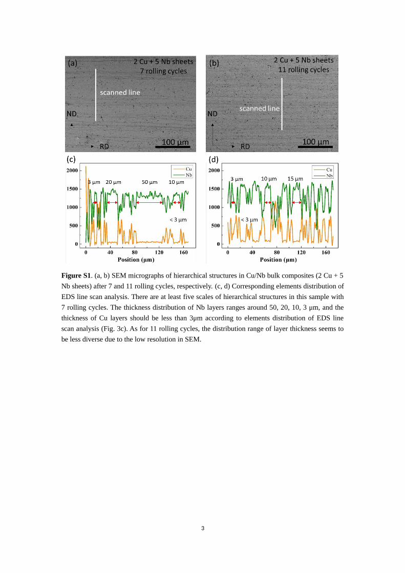
Figure S1. (a, b) SEM micrographs of hierarchical structures in Cu/Nb bulk composites (2 Cu + 5
Nb sheets) after 7 and 11 rolling cycles, respectively. (c, d) Corresponding elements distribution of
EDS line scan analysis. There are at least five scales of hierarchical structures in this sample with
7 rolling cycles. The thickness distribution of Nb layers ranges around 50, 20, 10, 3 μm, and the
thickness of Cu layers should be less than 3μm according to elements distribution of EDS line
scan analysis (Fig. 3c). As for 11 rolling cycles, the distribution range of layer thickness seems to
be less diverse due to the low resolution in SEM.
3

Figure S2. Fracture surfaces of samples after 7, 11 and 15 rolling cycles, respectively. Except for
a few cleavages, large areas of typical dimple features are observed in samples with 7 and 11
rolling cycles, which represent the coexistence of brittle and ductile fracture. With increasing
rolling cycles (Figure S2c), a large volume fraction of cleavages instead of dimples appear in a flat
fracture surface. It is consistent with the high strength and limited ductility of Cu/Nb
nanolaminates with ultra-thinner layers.
4

Figure S3. (a)A TEM foil sample of annealed Cu/Nb multilayers (annealed at 800°C for 3 hours)
prepared by the FIB. (b) Cross-sectional TEM image of the annealed Cu/Nb composite, multilayer
structure almost disappears and gradually transforms into equiaxed grains.
5

Figure S4. Helium cluster size distribution and helium density in three separate regions, i.e. Cubulk (a), Nb bulk (b), and interfacial region (c) for three structural systems, after irradiation to 1.5dpa at 300 K. All types of interfaces prefer to trap helium clusters, however, amorphous and ITZones are more immune to large clusters than sharp interfaces. Cu and Nb matrix also host Heclusters, but with less density than that in interfaces. By comparison, Nb matrix has less but largerHe clusters than that in Cu matrix due to a higher helium diffusivity in BCC-Nb. The total Hedensity also confirms that interfaces are excellent sinks for helium clustering, while the sharpinterface has a higher helium density than other interfaces. Overall, the ITZ and amorphous regionwith a larger volume provide more nucleation sites for clustering and dispersion of helium.
6


![In Situ ... - Li Group 李巨小组li.mit.edu/A/Papers/13/Zhu13WangAdvM.pdf · nels along the b-axis (space group Pnma). [20–22 ] Ex situ high resolution transmission electron microscopy](https://img.pdfslide.tips/doc/110x75/60a2bbae8ff1e90e4d354214/in-situ-li-group-climiteduapapers13zhu13wangadvmpdf-nels.jpg)