Embed Size (px)
Citation preview
Advanced Tutorial in Materials Science and Engineering (2)
Summer 2015: Intensive Lectures (5 weeks : June 17-July 24) At Tohoku University, Sendai, Japan
Course Objective: この集中講義は 私が現在ワシントン大学工学部物質材料学科で行っている物質材料科学総論(学部高学年及び大学院初年度学生向け)をもとにして
作られたものです。 物質材料科学は今や理工各分野に浸透しそれぞれユニークな発展をとげていることは周知の通りですが、それだけに物質材料科学全体をもう一
度レビューしてみよう、または専攻は違っても自分なりの物質材料科学を構築して
みようと思う学生諸君にこの集中講義は役に立つと思います。講義は英語で行いま
すが、言葉の壁を乗り越えて学生諸君と授業での交流を大切にします。私は26歳
で渡米し今年でアメリカ在住40年になりましたが、 今までの私の経験が皆さんのなにかに役に立てればと思いこの集中講義を行います。奮って参加してください。 This is an advanced tutorial of Materials Science and Engineering at the senior and/or entry-graduate levels. The course is specifically designed for those who did not major in the field of Materials Science and Engineering (MSE) as undergraduates, yet whose research is closely related to MSE discipline, and/or those who wish to re-examine their knowledge of Materials Science and Engineering from a broader perspective. This course will focus on the nature of materials' physical and chemical structures, and their relationship to mechanical, electrical, dielectric, optical, magnetic and thermal properties. Emphasis will be on modern thinking about the materials principles and practice together with their structure-property-performance relationship in a form that is readily accessible to students in all disciplines. Instructor: Professor Fumio S. Ohuchi Department of Materials Science and Engineering University of Washington Seattle, WA 98195, USA [email protected] (206) 685-8272 Lectures: 4:20-5:50PM 3 times/week for 5 weeks (Monday, Wednesday and Friday)
Note: • First class on Wednesday, June 17, 2015. • July 22(W)-lecture will be held on July 21(Tues). • Last class on Friday, July 24, 2015. • Tentative schedule sheet is attached. Course Contents: Lecture material samples (selected from the Lecture Note) are attached for your information.
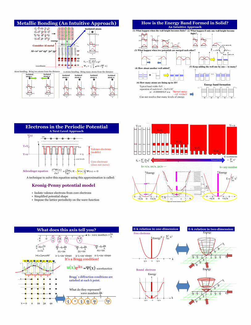
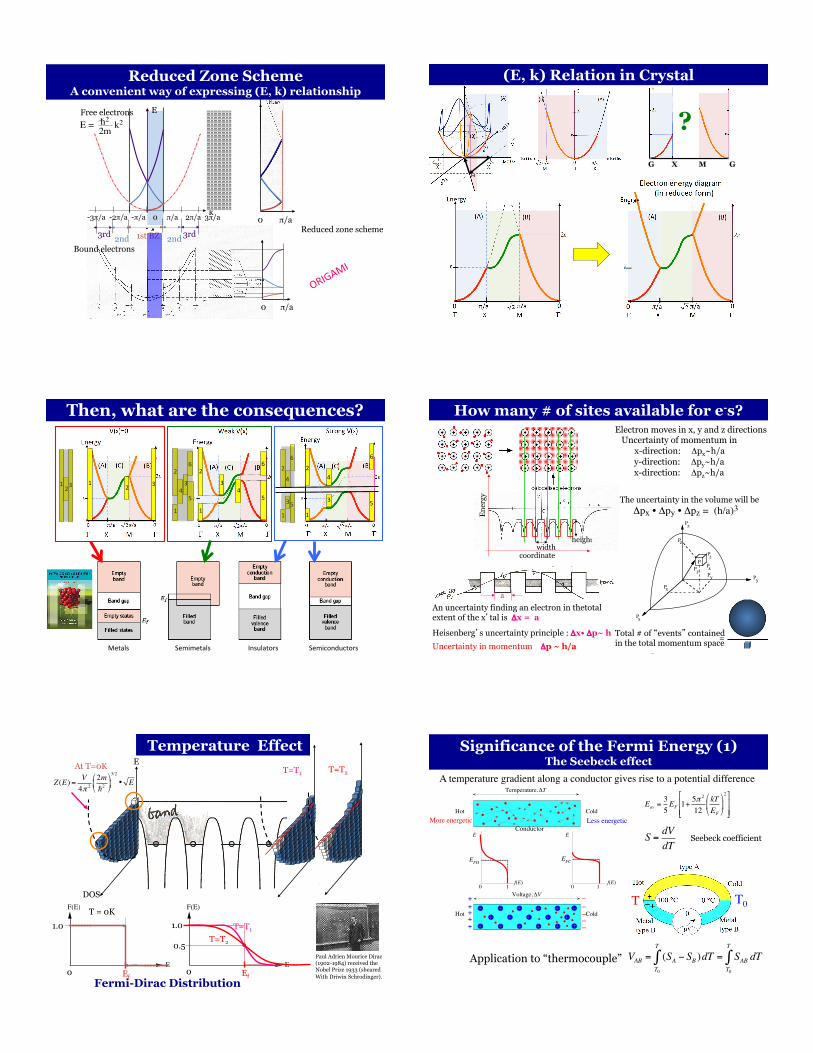
[I] What’s Unique About Materials Science & Engineering? • Thermodynamically versus kinetically controlled process and phenomena • Imperfections in solids: Thermodynamics legitimate questions • Driving forces of the material process [II] Materials With metallic bonding • Electron energy states and metallic bonding: relation to the properties • Group I, II, III and transition metals; how are the electrons distributed? • Significance of the Fermi energy
[III] An Atomic View of Materials • Energy and packing: order vs. disorder • Crystal structure and atomic packing • Basics (Review) of the crystallography [IV] Materials With Ionic & Covalent Bonding • Ionic-covalent mixed bonding, and charge density • Madelung constants • Factor influencing the crystal structures • Imperfections in materials; Hume-Rothey rules
[V] Phases & Equilibrirum • What can you learn from the phase diagram? • Materials processing [VI] Materials Under Mechanical Stress • Stress-strain relationship • Processes involved in the plastic deformation • What causes “material’s failure”? • “Karate” as an example! [VII] Electrical Conduction and Semiconductivity • Visualization of electrical conduction in metals and semiconductors • Semiconductor surfaces and junction properties • Basic devices: metal-sc junctions, p-n junctions and MOSFET [VIII] Dielectric & Optical Properties of Materials • Dielectric vs. optical: relationship through frequency • Specific to the dielectric and optic • Optical dispersion of materials • Absorption and recombination processes in semiconductors
Grading: HW (self-grading) 5-times 10%
Midterm exam (in-class) 40% Final exam (in-class) 50% Pre-requisite: No prerequisite is required to take this course, but the students are asked to
prepare basic background by themselves. Course pack: Available in PDF files provided in class Lectures will follow the course pack.

Sn Monday Tu Wednesday Th Friday St
14 15 Arrive Sendai
16 17 #1 [0] Introduction about this course [1] What’s unique about MSE?
18 19 #2 [2] Materials with metallic bonding(1)
20
21 22 Tohoku University Anniversary No class
23 24 #3 [2] Materials with metallic bonding(2)
25 26 #4 [3] An atomic view of materials
27
18 29 #5 [4] Materials with ionic and covalent bonding (1)
30 1 #6 [4] Materials with ionic and covalent bonding (2)
2 3 #7 [5] Phase diagram and equilibrium Adjustment Takehome Midterm Examination
4
5 6 #8 [6] Materials under mech. stress (1) Due for Takehome Midterm (10:00am)
7 8 #9 [6] Materials under mech. stress (2)
9 10 #10 [7] Electrical conduction and Semiconductors (1)
11
12 13 #11 [7] Electrical conduction and Semiconductors (2)
14 15 #12 [7] Electrical conduction and Semiconductors (3)
16 17 #13 [8] Dielectric & Optical Properties(1)
18
19 20 22 23 24 #15 Grand review/Course evaluation Takehome Final Examination
25
26 27 Due for Takhome Final-exam turn-in(10:00am)
28 29 30 Re-tur
31 1
21(Tuesday) #14 [8] Dielectric & Optical properties (2)
16 Course Preparation
28 Grading Course Administration
29
30 Return back to Seattle
31

The concept of materials science tetrahedron (MST) concisely depicts the inter-dependent relationship among the structure,
properties, performance, and processing of a material.
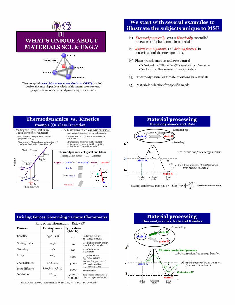
[I] WHAT’S UNIQUE ABOUT MATERIALS SCI. & ENG.?
(1). Thermodynamically versus Kinetically controlled processes and phenomena in materials (2). Kinetic rate equations and driving force(s) in materials, and the rate equations. (3). Phase transformation and rate control • Diffusional vs. Diffusionless(Martensitic) transformation
• Displacive vs. Reconstructive transformations (4). Thermodynamic legitimate questions in materials (5). Materials selection for specific needs
We start with several examples to illustrate the subjects unique to MSE
• Melting and Crystallization are Thermodynamic Transitions -Discontinuous changes in structure and properties and Tm
-Structures are �thermodynamically controlled� and described by the �Phase Diagram�
• The Glass Transition is a Kinetic Transition – Continuous changes in structure and properties
– Structure and properties are continuous with temperature
– Structures and properties can be changed continuously by changing the kinetics of the cooling liquid �kinetically controlled�
glass
Super cooled liquid
Thermodynamics vs. Kinetics Example (1): Glass Transition
Temperature
Volu
me liquid
crystal
Tm aliquid
acrystal
aliquid >>acrystal
Tm Tg
Thermodynamics of Crystal and Glass
Stable/Meta-stable versus Unstable
Stable
Meta-stable
Un-stable
Crystal is �stable� or �meta-stable� Glass is �unstable� state A
state B Initial Activated Final state state state
ΔGa
ΔG
How fast transformed from A to B? Rate∝ exp −ΔGa
RT$
%&
'
()
ΔGa: activation free energy barrier.
ΔG : driving force of transformation from State-A to State-B
state A state B Process of change
Surroundings
Boundary
Material processing Thermodynamics and Rate
Arrhenius rate equation
Driving Forces Governing various Phenomena
Process Fracture Grain growth Sintering Creep
Crystallization Inter diffusion
Oxidation
Driving Force F
Vmσ2/(2Y)
2γgb/r
2γ/r
σVm
ΔHΔT/Tm
RΤ(xalnxa+xblnxb)
ΔGform
Typ. values (J/Mole)
0.5 σ: stress at failure
Y: Young’s modulus
20 γgb: grain boundary energy r: radius of a particle
100
1000 σ: applied stress Vm: molar volume
3000 ΔH : enthalpy of transf. ΔT : under cooling Tm : melting point
5000 Ideal sulution
50,000- 500,000
Free energy of formation of oxide; a per-mole-of-O.
γ: surface energy r: curvature
Assumptions : 1000K, molar volume: 10-5m3/moll, r ~1µ, g=1J/m2. σ=100MPa
Rate of transformation: Rate=βF
state A
state B Initial Activated Final state state state
ΔGa
ΔG
ΔG’a
ΔG’
Metastate B’
ΔGa: activation free energy barrier.
ΔG : driving force of transformation from State-A to State-B
state A
state B
Surroundings
state B’
Material processing Thermodynamics, Rate and Kinetics
Kinetics controlled process
Al2Au AlAu
AlAu2
Al2Au5
AlAu4
733K(460C)
473K(200C)
AlAu4 Al2Au
150C 100C
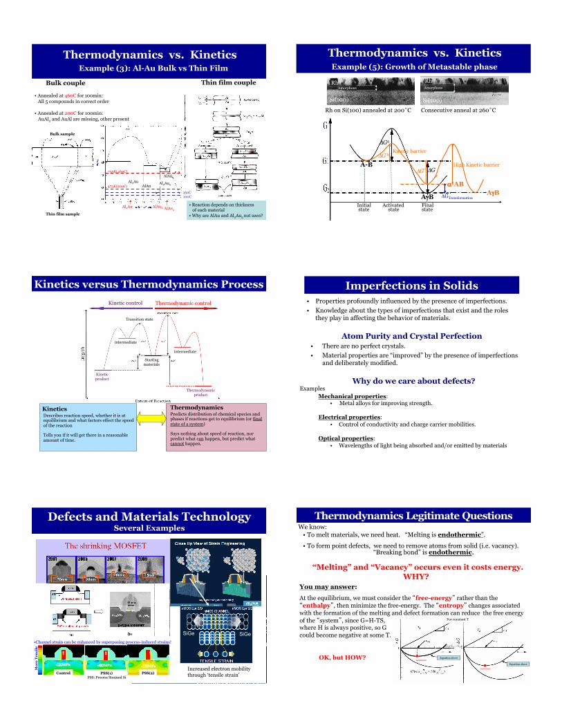
Example (3): Al-Au Bulk vs Thin Film
• Annealed at 460C for 100min:
All 5 compounds in correct order • Annealed at 200C for 100min: AuAl2 and AuAl are missing, other present
Thin film couple
Thermodynamics vs. Kinetics
• Reaction depends on thickness of each material • Why are AlAu and Al2Au5 not seen?
Bulk sample
Thin film sample
Bulk couple
A-B
AγB Initial Activated Final state state state
ΔGa
ΔG
ΔG’a
ΔG’
α-AB AγB
Kinetic barrier
High Kinetic barrier
ΔGTransformation
Si(100) Si(100)
Rh Rh
Rh on Si(100) annealed at 200˚C Consecutive anneal at 260˚C
Amorphous Amorphous
Example (5): Growth of Metastable phase Thermodynamics vs. Kinetics
Kinetics versus Thermodynamics Process
Kinetics Describes reaction speed, whether it is at equilibrium and what factors effect the speed of the reaction
Tells you if it will get there in a reasonable amount of time.
Thermodynamics Predicts distribution of chemical species and phases if reactions get to equilibrium (or final state of a system)
Says nothing about speed of reaction, nor predict what can happen, but predict what cannot happen.
Kinetic control Thermodynamic control
Transition state
intermediate
intermediate
Starting materials
Kinetic product
Thermodynamic product
Imperfections in Solids • Properties profoundly influenced by the presence of imperfections. • Knowledge about the types of imperfections that exist and the roles
they play in affecting the behavior of materials.
Atom Purity and Crystal Perfection
Why do we care about defects?
Mechanical properties: • Metal alloys for improving strength.
Electrical properties:
• Control of conductivity and charge carrier mobilities.
Optical properties: • Wavelengths of light being absorbed and/or emitted by materials
• There are no perfect crystals. • Material properties are “improved” by the presence of imperfections
and deliberately modified.
Examples
Defects and Materials Technology Several Examples
Control
����MPa
PSS(1) PSS: Process Strained Si
����MPa
PSS(2)
����MPa
Mor
e Te
nsile
Increased electron mobility through ‘tensile strain’
SiGe SiGe • Channel strain can be enhanced by superposing process-induced strains!
We know: • To melt materials, we need heat. “Melting is endothermic”. • To form point defects, we need to remove atoms from solid (i.e. vacancy).
“Breaking bond” is endothermic.
“Melting” and “Vacancy” occurs even it costs energy. WHY?
Thermodynamics Legitimate Questions
You may answer: At the equilibrium, we must consider the �free-energy� rather than the �enthalpy�, then minimize the free-energy. The �entropy� changes associated with the formation of the melting and defect formation can reduce the free energy of the �system�, since G=H-TS, where H is always positive, so G could become negative at some T. OK, but HOW? minimum
Eq. *
Equation above
Equation above
minimum
€
ΔG =Gdef −Gperf = nν
For constant T

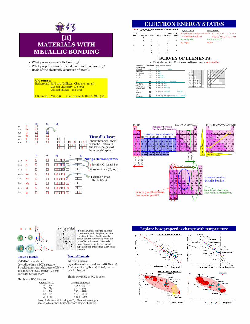
• What promotes metallic bonding? • What properties are inferred from metallic bonding? • Basis of the electronic structure of metals
[II] MATERIALS WITH
METALLIC BONDING
UW courses Background MSE 170 (Callister: Chapter 2, 12, 14)
General Chemistry 100 level General Physics 100 level
UG course MSE 351 Grad courses MSE 510, MSE 518
ELECTRON ENERGY STATES Quantum # Designation n = principal (energy level-shell) K, L, M, N, O (1, 2, 3, etc.) l = subsidiary (orbitals) s, p, d, f (0, 1, 2, 3,…, n -1) ml = magnetic 1, 3, 5, 7 (-l to +l) ms = spin ½, -½
SURVEY OF ELEMENTS
5
• Most elements: Electron configuration is not stable. Element
Hydrogen Helium Lithium Beryllium Boron Carbon ... Neon Sodium Magnesium Aluminum ... Argon ... Krypton
Atomic #1 2 3 4 5 6
10 11 12 13
18 ... 36
Electron configuration 1s 1 1s 2 (stable) 1s 2 2s 1 1s 2 2s 2 1s 2 2s 2 2p 1 1s 2 2s 2 2p 2 ... 1s 2 2s 2 2p 6 (stable) 1s 2 2s 2 2p 6 3s 1 1s 2 2s 2 2p 6 3s 2 1s 2 2s 2 2p 6 3s 2 3p 1 ... 1s 2 2s 2 2p 6 ... 1s 2 2s 2 2p 6 3s 2 3p 6 3d 10
3s 2 3p 6 (stable)
4s 2 4 6 (stable)
1s 2s 2p 3s 3p 3d 4s 4p 4d 4f 5s 5p 5d 5f 5g 6s 6p 6d 6f 6g
1s 2s 2p
2s 2p 3s 3p 3d 4s
3d 4s
H ↑ He ↑↓ Li ↑↓ ↑ Be ↑↓ ↑↓ B ↑↓ ↑↓ ↑ C ↑↓ ↑↓ ↑ ↑ ↑ ↑ ↑ ↑
↑↓ ↑↓ ↑↓ ↑ ↓ ↑ ↓ ↑ ↓
Z=7 Z=8 Z=9 Z=10 Z=11 Z=12 Z=13 Z=14
N O F Ne Na Mg Al Si
1s 2s 2p 3s 3p ↑↓ ↑↓ ↑ ↑ ↑
↑↓ ↑↓ ↓↑ ↑ ↑
↑↓ ↑↓ ↓↑ ↓↑ ↑
↑↓ ↑↓ ↓↑ ↓↑ ↑↓
↑↓ ↑↓ ↓↑ ↓↑ ↑↓ ↑
↑↓ ↑↓ ↓↑ ↓↑ ↑↓ ↑↓
↑↓ ↑↓ ↓↑ ↓↑ ↑↓ ↑↓ ↑
↑↓ ↑↓ ↓↑ ↓↑ ↑↓ ↑↓ ↑ ↑
↓ ↓
Forming O-- ion (S, Se)
↓ Forming F- ion (Cl, Br, I)
Puling’s electronegativity
Forming Na+ ion (Li, K, Rb, Cs)
Hund�s law: Energy becomes lowest when the electron in the same energy level have parallel spins.
IA IIA IIIA IVA VA VIAVIIAVIII IIIB IVB VB VIB VIIB VIII IB IIB
IA IIA IIIA IVA VAVIAVIIAVIII
Atomic Size Atom
ic S
ize
Transition metal elements gi
ve u
p 1e
- gi
ve u
p 2e
- gi
ve u
p 3e
-
acce
pt 1e
- ac
cept
2e-
Boundary between Metals and Non-metals
Easy to give off electrons (Low ionization potential)
Easy to get electrons (High Pauling electronegativity)
�ionic� bonding
Covalent bonding Metallic bonding
Secondary peak near the nucleus: e- penetrates fairly deeply in the atom from time to time. Similar way that Halley’s comet nips quickly round the part of its orbit close to the sun (but takes 75 years). For 2s electron, it repeats about 2MM times every nano-seconds.
Group-I metals Half filled in s-orbital Crystallizes into a BCC structure 8 nuclei as nearest neighbours (CN#=8) and another second nearest (CN#6) only 15 % further away. This is why BCC is taken
Group-II metals Filled in s-orbital Crystallizes into a closed packed (CN#=12) Next nearest neighbours(CN#=6) occurs 41% further off. This is why HEX or FCC is taken
Group I vs II Melting Temp (K) Li : Be 452 : 1550 Na : Mg 371 : 924 K : Ca 337 : 1120 Rb : Sr 312 : 1042 Cs : Ba 302 : 1000
Group II elements all have higher Tm. More rattle energy is needed to break their bonds, therefore stronger bonding.
1s vs. 2s orbital Explore how properties change with temperature
Log scale
Linear scale
CERAMICS
Log scale
Log scale
coordinate
Consider Al metal
Al=1s2 2s2 2p6 3s2 3p1
V(r) V
core levels 3s
3p
1s
energy
2s 2p
a n=1
n=2
E 1
E 2
Isolated atom
E 3 N=3
En = h2
2m πa2
Ψn = 2a i sin (2πa x)• n
• n2
Atom bonding: Bring two atoms from the distance
a n=1
n=2
E 1
E 2
Isolated atom-1
a n=1
n=2
E 1
E 2
Isolated atom-2
n-atoms bonding: Bring many atoms from the distance
a n=1
n=2
E 1
E 2
Isolated atom-1
a n=1
n=2
E 1
E 2
Isolated atom-2
a n=1
N=2 • • • • • • • • •
E 1
E 2
Isolated atom-3
a n=1
n=2
E 1
E 2
Isolated atom-n
Metallic Bonding (An Intuitive Approach) (1) What happen when the wall height becomes finite?!
n=1$
n=2$
n=3$
(2) What happen if only one wall height become ! finite?!
(3) What happen when two potentials are merged each other? !
+!
(4) How about another well added?! (5) Keep adding the well one by one--- to many?!
…!
Can not resolve that many levels of energy!!!
(6) How many atoms are lining up in 1D?!
• • • • • • Typical band width~5eV : !separation of each level ~ 5(eV)/107 ! or ~0.0000005eV ! Thermal energy !
~ kT 0.026eV!<!<!
Energy band formation!
How is the Energy Band Formed in Solid? An Intuitive Approach
V(r)
ion
V
core levels
Valence electrons (mobile) Core electrons (does not move)
∂2Ψ(x)∂x2
+ 2mh2
( E - V(x)) Ψ(x) = 0Schrodinger equation
x
V(x)
V=0
V=V0
A technique to solve this equation using this approximation is called:
Kronig-Penny potential model
• Isolate valence electrons from core electrons • Simplified potential shape • Impose the lattice periodicity on the wave function
Electrons in the Periodic Potential A Next Level Approach
What happen? V=∞
V=V1
V=V2
V=V3 V=V4
V= 0
n=1
n=2
n=3
k= π/a, 2π/a, 3π/a --- k= any number
En = h2
2m πa n 2
Energy
k -π/a 0 +π/a
n=1
n=2
E =contineous = h2
2m k2
k
Energy
E = h2
2m k2
-π/a 0 +π/a
Toward bound e- Toward free e-
Vo
0
ΨΙ' ΨΙ' ΨΙ' ΨΙ' ΨΙ'ΨΙΙ''
ΨΙΙ''
ΨΙΙ''
ΨΙΙ''
ΨΙΙ''
eikx =Ψ(x) wavefunction
a a a a'
u(x)
x = 0 a 2a 3a 4a - π'a 0 π'
a 2 π'a
3 a . . . . n π'
a
wave numbers 2 π'λ'
Bragg�s diffraction conditions are satisfied at each k point.
πa = 2πλ
λ = 2a
k x
- πa 0 πa
2πa
3πa
. . . . n πa
wave numbers = 2πλ
2πa = 2πλ
2λ = 2a 2• λ =2a•sin90˚
3πa = 2πλ
3λ = 2a 3• λ =2a•sin90˚
nπa = 2πλ
nλ = 2a n• λ =2a•sin90˚
2• λ =2a•sin90˚ 1 1•λ=2a•sin90˚ 2・ λ'=2a・sin90 3・ λ'
=2a・sin90 n・ λ'=2a・sin90
What do they represent?
λ=2a 2 λ'=2a 3 λ'
=2a n λ'
=2a 2 π'
a =k= 2 π'λ'
3 π'a =k= 2 π'
λ' n π'
a =k= 2 π'λ'
πa =k=2π
kλ
It’s a Bragg condition!
k=
π'
What does this axis tell you? E-k relation in one-dimension Free electrons
Energy E = h2
2m k2
-p/a 0 +p/a
Energy
-p/a 0 +p/a k
Bound electrons
k kx - 0 p a
2 p a 3 p a p a
2 p a 3 p a - -
ky
-
p a
2 p a
3 p a
p a 2 p a
3 p a
Energy
Energy
kx - 0 p a 2 p a
3 p a p a 2 p a 3 p a - -
ky
-
p a
2 p a
3 p a
p a 2 p a
3 p a
E-k relation in two-dimension
0 π/a Reduced zone scheme
Bound electrons
1st BZ 2nd 2nd 3rd 3rd
-3π/a -2π/a -π/a 0 π/a 2π/a 3π/a k
E Free electrons E = h2
2m k2
0 π/a
Reduced Zone Scheme A convenient way of expressing (E, k) relationship
G X M G
?
(E, k) Relation in Crystal
1$2$ 3$
4$
3$
2$
1$
5$
6$
1$
2$
3$4$
5$
6$
1$2$3$
1$
2$
3$4$
5$
6$
4$
3$
2$
1$
5$
6$
Metals$$$$$$$$$$$$$$$$$$$$$$$$$$$Semimetals$$$$$$$$$$$$$$$$$$$$$$Insulators$$$$$$$$$$$$$$$$$$Semiconductors$$
Then, what are the consequences?
An uncertainty finding an electron in thetotal extent of the x�tal is Δx = a
Heisenberg�s uncertainty principle : Δx• Δp~ h Uncertainty in momentum Δp ~ h/a
coordinate
Ener
gy
a
width height
Δpx • Δpy • Δpz = (h/a)3The uncertainty in the volume will be
Electron moves in x, y and z directions Uncertainty of momentum in x-direction: Δpx~h/a
y-direction: Δpy~h/a x-direction: Δpz~h/a
P
Px
Py
Pz
Px
Px
PyPy
Pz
Pz
Total # of �events� contained in the total momentum space =
How many # of sites available for e-s?
At T=0K E
DOS
Z(E) = V4π 2
2m!2
!
"#
$
%&3/2
• E
Temperature Effect
F(E)
EEf 0
1.0
F(E)
E
T = 0K
Ef 0
1.0
0.5
T=T1
T=T1
T=T2
T=T2
Fermi-Dirac Distribution
Paul Adrien Mourice Dirac (1902-1984) received the Nobel Prize 1933 (sheared With Driwin Schrodinger).
A temperature gradient along a conductor gives rise to a potential difference!
E
1
EFH
E
f(E)1
EFC
Conductor
0 0
Hot Cold
––––
++++
Temperature, ΔT
f(E)
Voltage, ΔV –+
From Principles of Electronic Materials and Devices, Second Edition, S.O. Kasap (© McGraw-Hill, 2002)http://Materials.Usask.Ca
Fig.4.30: The Seebeck effect: A temperature gradient along aconductor gives rise to a potential difference.
Hot Cold
More energetic! Less energetic!
S = dVdT
Eav =35EF 1+
5π 2
12kTEF
!
"#
$
%&
2'
())
*
+,,
Significance of the Fermi Energy (1) The Seebeck effect
Seebeck coefficient $
T! T0!
Application to “thermocouple” VAB = (SA − SB )dTT0
T
∫ = SAB dTT0
T
∫

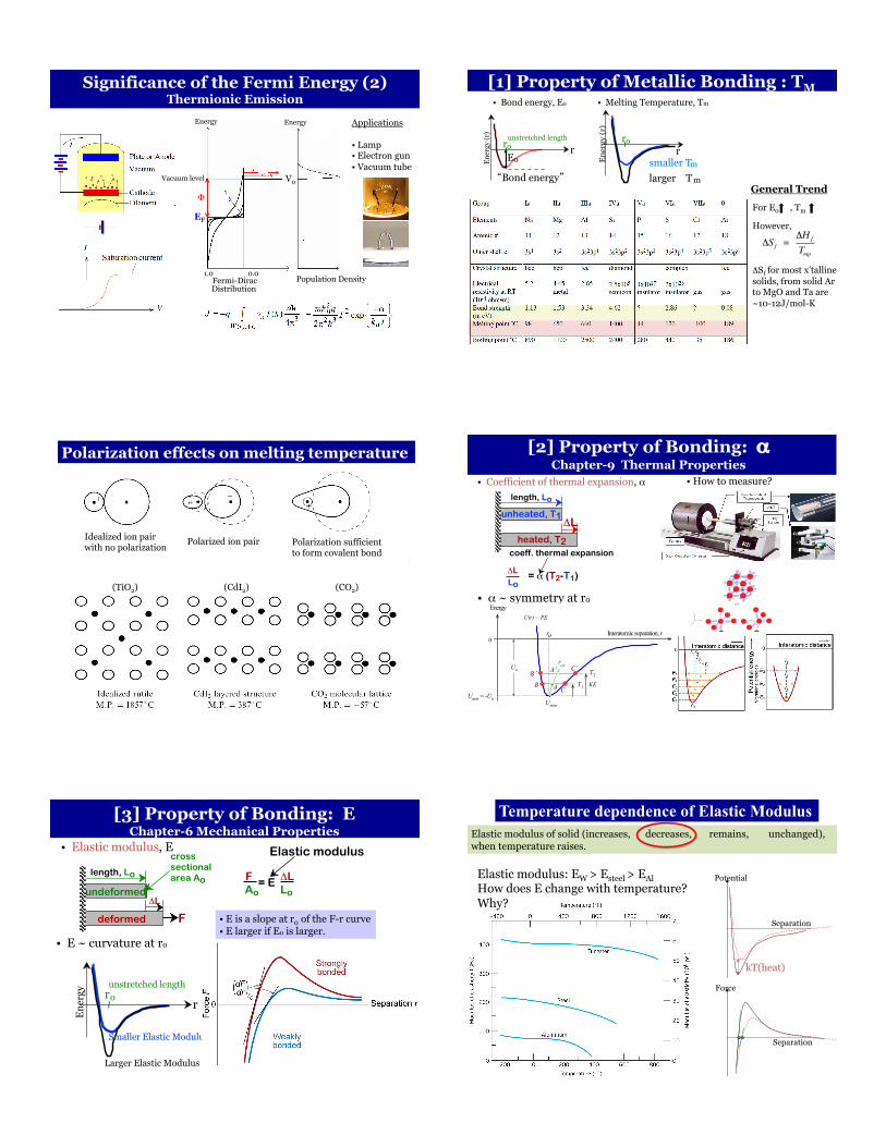
Significance of the Fermi Energy (2) Thermionic Emission
Energy
EF
Vacuum level
1.0 0.0 Fermi-Dirac Distribution
Population Density
E0
Φ'
Energy
V0
Applications • Lamp • Electron gun • Vacuum tube
[1] Property of Metallic Bonding : TM • Bond energy, Eo • Melting Temperature, Tm
E o
�Bond energy�
Ener
gy (r
)
r o r unstretched length
r
m
Ener
gy (r
)
r o
larger T smaller T m
For E0 , Tm However, ΔSf for most x’talline solids, from solid Ar to MgO and Ta are ~10-12J/mol-K
€
ΔS f = ΔH f
Tmp
General Trend
Polarization effects on melting temperature
Idealized ion pair with no polarization Polarized ion pair Polarization sufficient
to form covalent bond
(TiO2) (CdI2) (CO2)
x
y
z
(b)
(a)
(a) The ball-and-spring model of solids in which the springsrepresent the interatomic bonds. Each ball (atom) is linked to itsneighbors by springs. Atomic vibrations in a solid involve 3dimensions.(b) An atom vibrating about its equilibrium position stretches andcompresses its springs to the neighbors and has both kinetic andpotential energy.
17
• Coefficient of thermal expansion, α'
• α ~ symmetry at ro
ΔL
length, Lo
unheated, T1
heated, T2
= α (T2-T1) ΔL Lo
coeff. thermal expansion
[2] Property of Bonding: α Chapter-9 Thermal Properties
Interatomic separation, r0
Uo
ro
BC
KE
U(r) = PE
B!C!
ravT2
T1
Umin
A
A!
Umin = -Uo
Energy
The potential energy PE curve has a minimum when the atoms inthe solid attain the interatomic separation at r = ro. Due to thermalenergy, the atoms will be vibrating and will have vibrational kineticenergy. At T = T1, the atoms will be vibrating in such a way that thebond will be stretched and compressed by an amount correspondingto the KE of the atoms. A pair of atoms will be vibrating between Band C. Their average separation will be at A and greater than ro.
• How to measure?
[3] Property of Bonding: E
Chapter-6 Mechanical Properties • Elastic modulus, E
• E ~ curvature at ro
cross sectional area Ao
ΔL
length, Lo
F
undeformed
deformed
ΔL F Ao
= E Lo
Elastic modulus
r
Ener
gy
r o unstretched length
Larger Elastic Modulus Smaller Elastic Modulus
• E is a slope at r0 of the F-r curve • E larger if Eo is larger.
Potential
Separation
kT(heat)
Force
Separation
Temperature dependence of Elastic Modulus Elastic modulus of solid (increases, decreases, remains, unchanged), when temperature raises.
Elastic modulus: EW > Esteel > EAl How does E change with temperature? Why?

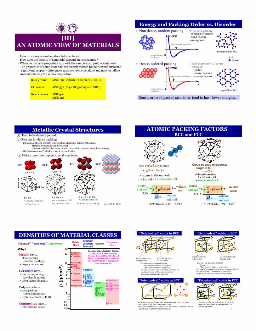
• How do atoms assemble into solid structures? • How does the density of a material depend on its structure? • When do material properties vary with the sample (i.e., part) orientation? • The properties of some materials are directly related to their crystal structures. • Significant property differences exist between crystalline and noncrystalline materials having the same composition.
[III]
AN ATOMIC VIEW OF MATERIALS
Back ground MSE 170 (Callister: Chapters 3, 12, 14) UG course MSE 331 (Crystallography and XRD) Grad courses MSE 510
MSE 518 2
• Non dense, random packing
• Dense, ordered packing
Dense, ordered packed structures tend to have lower energies.
Energy and Packing: Order vs. Disorder
Energy
r
Energy
r crystalline SiO2
noncrystalline SiO2
Si Oxygen
• No periodic packing -complex structures
-rapid cooling -amorphous
• Pack in periodic, 3D arrays • typical of:
-metals -many ceramics -some polymers
typical neighbor bond length
typical neighbor bond energy
typical neighbor bond length
typical neighbor bond energy
aR
close-packed directions
a
R=0.5a
contains 8 x 1/8 = 1 atom/unit cell
CN# = 6 CN# = 8
SC BCC FCC
a
CN# = 12
HCP
(1) Tend to be densely packed. (2) Reasons for dense packing:
- Typically, only one element is present, so all atomic radii are the same. Metallic bonding is not directional. Nearest neighbor distances tend to be small in order to lower bond energy.
- The �electron cloud� shields cores from each other
(3) Metals have the simplest crystal structures.
Metallic Crystal Structures
8 x 1/8 + 1 =2 atoms/unit cell
8 x 1/8 + 6x 1/2 =4 atoms/unit cell
ex: Cr, W, Fe (α), Ta, M ex: Al, Cu, Au, Pb, Ni, Pt, Ag ex: Po(only known) ex: Mg, Ti, Zr, Hf, Zn
8 x 1/8 =1 atoms/unit cell
aR
• APF(BCC)= 0.68 (68%)
lose-packed directions:
length = 4R = 3 a
# atoms in the unit cell 1 + 8 x 1/8 = 2 atoms/unit cell
3
atoms unit cell atom
volume
unit cell volume APF =
a
4 3 p ( 3 a/4 ) 3 2
3
a
a 2
a 3
APF = a3
4
3π ( 2a/4)34
atoms
unit cell atomvolume
unit cell
volume
Unit cell contains: 6 x 1/2 + 8 x 1/8 = 4 atoms/unit cell
Close-packed directions: length = 4R
! ! = 2 a
a
• APF(FCC)= 0.74 (74%)
ATOMIC PACKING FACTORS BCC and FCC
ρmetals≥ ρceramics≥ ρpolymers
ρ (
g/c
m3)
Graphite/Ceramics/Semicond
Metals/Alloys
Composites/fibersPolymers
1
2
20
30Based on data in Table B1, Callister
*GFRE, CFRE, & AFRE are Glass, Carbon, & Aramid Fiber-Reinforced Epoxy composites (values based on 60% volume fraction of aligned fibers
in an epoxy matrix). 10
3 4 5
0.3 0.4 0.5
Magnesium
Aluminum
Steels
Titanium
Cu,Ni
Tin, Zinc
Silver, Mo
Tantalum Gold, W Platinum
Graphite Silicon
Glass-soda Concrete
Si nitride Diamond Al oxide
Zirconia
HDPE, PS PP, LDPE
PC
PTFE
PET PVC Silicone
Wood
AFRE*
CFRE*
GFRE*
Glass fibers
Carbon fibers
Aramid fibers
Why? Metals have... • close-packing (metallic bonding) • large atomic mass Ceramics have... • less dense packing (covalent bonding) • often lighter elements Polymers have... • poor packing (often amorphous) • lighter elements (C,H,O) Composites have... • intermediate values
DENSITIES OF MATERIAL CLASSES
6
6 octahedral voids in face center
12 octahedral voids in edge center
• You see 12+6=18 octahedral sites. Edge center ¼ share = 12x(1/4)=3 Face center ½ share = 6 x(1/2)=3 • So, total of 6 octahedral voids (sites) per BCC cell • Octahedral voids in BCC are asymmetric • Each has a short parallel cube edge
• There are four tetrahedral sites on each of the six BCC cell faces • You see total 4 x 6 =24 tetrahedral voids • Each face ½ shared, so 24 x (1/2)=12 tetrahedral voids (sites) per cell • Tetrahedral voids in BCC are asymmetric
(½,¼,0)
“Octahedral” voids in FCC
1 octahedral voids in the center
12 octahedral voids in edge center
• You see 1+12=13 octahedral sites. Center = 1 Edge center ¼ share = 12 x(1/4)=3 • So, total of 1+3=4 octahedral voids (sites) per FCC cell • Center octahedral void in FCC is symmetric • Edge center octahedral voids are asymmetric
“Tetrahedral” voids in FCC
• Located at {1/4,1/4,1/4} - center of cell octet • There are 8 tetrahedral voids per FCC cell • All are symmetric
“Tetrahedral” voids in BCC
“Octahedral” voids in BCC
Advanced Tutorial in Materials Science and Engineering (2)
Summer 2015: Intensive Lectures (5 weeks : June 17-July 24) At Tohoku University, Sendai, Japan
Course Objective: This is an advanced tutorial of Materials Science and Engineering at the senior and/or entry-graduate levels. The course is specifically designed for those who did not major in the field of Materials Science and Engineering (MSE) as undergraduates, yet whose research is closely related to MSE discipline, and/or those who wish to re-examine their knowledge of Materials Science and Engineering from a broader perspective. This course will focus on the nature of materials' physical and chemical structures, and their relationship to mechanical, electrical, dielectric, optical, magnetic and thermal properties. Emphasis will be on modern thinking about the materials principles and practice together with their structure-property-performance relationship in a form that is readily accessible to students in all disciplines. Instructor: Professor Fumio S. Ohuchi Department of Materials Science and Engineering University of Washington Seattle, WA 98195, USA [email protected] (206) 685-8272 Lectures: 4:20-5:50PM 3 times/week for 5 weeks (Monday, Wednesday and Friday) Note: • First class on Wednesday, June 17, 2015. • July 22(W)-lecture will be held on July 21(Tues). • Last class on Friday, July 24, 2015. • Tentative schedule sheet is attached. Course Contents:
[I] What’s Unique About Materials Science & Engineering? • Thermodynamically versus kinetically controlled process and phenomena • Imperfections in solids: Thermodynamics legitimate questions • Driving forces of the material process [II] Materials With metallic bonding • Electron energy states and metallic bonding: relation to the properties • Group I, II, III and transition metals; how are the electrons distributed? • Significance of the Fermi energy [III] An Atomic View of Materials • Energy and packing: order vs. disorder • Crystal structure and atomic packing • Basics (Review) of the crystallography [IV] Materials With Ionic & Covalent Bonding • Ionic-covalent mixed bonding, and charge density • Madelung constants • Factor influencing the crystal structures • Imperfections in materials; Hume-Rothey rules
[V] Phases & Equilibrirum • What can you learn from the phase diagram? • Materials processing [VI] Materials Under Mechanical Stress • Stress-strain relationship • Processes involved in the plastic deformation • What causes “material’s failure”? • “Karate” as an example! [VII] Electrical Conduction and Semiconductivity • Visualization of electrical conduction in metals and semiconductors • Semiconductor surfaces and junction properties • Basic devices: metal-sc junctions, p-n junctions and MOSFET [VIII] Dielectric & Optical Properties of Materials • Dielectric vs. optical: relationship through frequency • Specific to the dielectric and optic • Optical dispersion of materials • Absorption and recombination processes in semiconductors
NOTE: Samples (pick up several slides) from Lecture Note are attached for your information.
Grading: HW (self-grading) 5-times 10%
Midterm exam (in-class) 40% Final exam (in-class) 50% Pre-requisite: No prerequisite is required to take this course, but the students are asked to
prepare basic background by themselves. Course pack: Available in PDF files provided in class Lectures will follow the course pack. Suggested reference books for background information: Any of the following comprehensive text books introducing Materials Science and Engineering will serve as the reference for background. • William D Callister, Jr. and David G. Rethwisch, Materials Science and Engineering: An Introduction,
6, 7 or 8th Editions, Wiley. • James F. Shackelford, Introduction to Materials Science for Engineers, 6 or 7th Edition, Macmillan. • Donal R. Askeland and Pradeep P. Phule, The Science and Engineering of Materials, 5th/6th Edition,
Thomson. • L. H. Van Vlack, Elements of Materials Science and Engineering, 6th Edition, • Craig R. Barret, William D. Nix and Alan S. Teleman, The Principles of Engineering Materials,
Prentice-Hall, Inc. (classical book) • Charles A. Wert and Robb M. Thomson, Physics of Solids, McGraw-Hill, 2nd edition (classic book)

Sn Monday Tu Wednesday Th Friday St
14 15 Arrive Sendai
16 17 #1 [0] Introduction about this course [1] What’s unique about MSE?
18 19 #2 [2] Materials with metallic bonding(1)
20
21 22 Tohoku University Anniversary No class
23 24 #3 [2] Materials with metallic bonding(2)
25 26 #4 [3] An atomic view of materials
27
18 29 #5 [4] Materials with ionic and covalent bonding (1)
30 1 #6 [4] Materials with ionic and covalent bonding (2)
2 3 #7 [5] Phase diagram and equilibrium Adjustment Takehome Midterm Examination
4
5 6 #8 [6] Materials under mech. stress (1) Due for Takehome Midterm (10:00am)
7 8 #9 [6] Materials under mech. stress (2)
9 10 #10 [7] Electrical conduction and Semiconductors (1)
11
12 13 #11 [7] Electrical conduction and Semiconductors (2)
14 15 #12 [7] Electrical conduction and Semiconductors (3)
16 17 #13 [8] Dielectric & Optical Properties(1)
18
19 20 22 23 24 #15 Grand review/Course evaluation Takehome Final Examination
25
26 27 Due for Takhome Final-exam turn-in(10:00am)
28 29 30 Re-tur
31 1
21(Tuesday) #14 [8] Dielectric & Optical properties (2)
16 Course Preparation
28 Grading Course Administration
29
30 Return back to Seattle
31
The concept of materials science tetrahedron (MST) concisely depicts the inter-dependent relationship among the structure,
properties, performance, and processing of a material.
[I] WHAT’S UNIQUE ABOUT MATERIALS SCI. & ENG.?
(1). Thermodynamically versus Kinetically controlled processes and phenomena in materials (2). Kinetic rate equations and driving force(s) in materials, and the rate equations. (3). Phase transformation and rate control • Diffusional vs. Diffusionless(Martensitic) transformation
• Displacive vs. Reconstructive transformations (4). Thermodynamic legitimate questions in materials (5). Materials selection for specific needs
We start with several examples to illustrate the subjects unique to MSE
• Melting and Crystallization are Thermodynamic Transitions -Discontinuous changes in structure and properties and Tm
-Structures are �thermodynamically controlled� and described by the �Phase Diagram�
• The Glass Transition is a Kinetic Transition – Continuous changes in structure and properties
– Structure and properties are continuous with temperature
– Structures and properties can be changed continuously by changing the kinetics of the cooling liquid �kinetically controlled�
glass
Super cooled liquid
Thermodynamics vs. Kinetics Example (1): Glass Transition
Temperature
Volu
me liquid
crystal
Tm aliquid
acrystal
aliquid >>acrystal
Tm Tg
Thermodynamics of Crystal and Glass
Stable/Meta-stable versus Unstable
Stable
Meta-stable
Un-stable
Crystal is �stable� or �meta-stable� Glass is �unstable� state A
state B Initial Activated Final state state state
ΔGa
ΔG
How fast transformed from A to B? Rate∝ exp −ΔGa
RT$
%&
'
()
ΔGa: activation free energy barrier.
ΔG : driving force of transformation from State-A to State-B
state A state B Process of change
Surroundings
Boundary
Material processing Thermodynamics and Rate
Arrhenius rate equation
Driving Forces Governing various Phenomena
Process Fracture Grain growth Sintering Creep
Crystallization Inter diffusion
Oxidation
Driving Force F
Vmσ2/(2Y)
2γgb/r
2γ/r
σVm
ΔHΔT/Tm
RΤ(xalnxa+xblnxb)
ΔGform
Typ. values (J/Mole)
0.5 σ: stress at failure
Y: Young’s modulus
20 γgb: grain boundary energy r: radius of a particle
100
1000 σ: applied stress Vm: molar volume
3000 ΔH : enthalpy of transf. ΔT : under cooling Tm : melting point
5000 Ideal sulution
50,000- 500,000
Free energy of formation of oxide; a per-mole-of-O.
γ: surface energy r: curvature
Assumptions : 1000K, molar volume: 10-5m3/moll, r ~1µ, g=1J/m2. σ=100MPa
Rate of transformation: Rate=βF
state A
state B Initial Activated Final state state state
ΔGa
ΔG
ΔG’a
ΔG’
Metastate B’
ΔGa: activation free energy barrier.
ΔG : driving force of transformation from State-A to State-B
state A
state B
Surroundings
state B’
Material processing Thermodynamics, Rate and Kinetics
Kinetics controlled process

Al2Au AlAu
AlAu2
Al2Au5
AlAu4
733K(460C)
473K(200C)
AlAu4 Al2Au
150C 100C
Example (3): Al-Au Bulk vs Thin Film
• Annealed at 460C for 100min:
All 5 compounds in correct order • Annealed at 200C for 100min: AuAl2 and AuAl are missing, other present
Thin film couple
Thermodynamics vs. Kinetics
• Reaction depends on thickness of each material • Why are AlAu and Al2Au5 not seen?
Bulk sample
Thin film sample
Bulk couple
A-B
AγB Initial Activated Final state state state
ΔGa
ΔG
ΔG’a
ΔG’
α-AB AγB
Kinetic barrier
High Kinetic barrier
ΔGTransformation
Si(100) Si(100)
Rh Rh
Rh on Si(100) annealed at 200˚C Consecutive anneal at 260˚C
Amorphous Amorphous
Example (5): Growth of Metastable phase Thermodynamics vs. Kinetics
Kinetics versus Thermodynamics Process
Kinetics Describes reaction speed, whether it is at equilibrium and what factors effect the speed of the reaction
Tells you if it will get there in a reasonable amount of time.
Thermodynamics Predicts distribution of chemical species and phases if reactions get to equilibrium (or final state of a system)
Says nothing about speed of reaction, nor predict what can happen, but predict what cannot happen.
Kinetic control Thermodynamic control
Transition state
intermediate
intermediate
Starting materials
Kinetic product
Thermodynamic product
Imperfections in Solids • Properties profoundly influenced by the presence of imperfections. • Knowledge about the types of imperfections that exist and the roles
they play in affecting the behavior of materials.
Atom Purity and Crystal Perfection
Why do we care about defects?
Mechanical properties: • Metal alloys for improving strength.
Electrical properties:
• Control of conductivity and charge carrier mobilities.
Optical properties: • Wavelengths of light being absorbed and/or emitted by materials
• There are no perfect crystals. • Material properties are “improved” by the presence of imperfections
and deliberately modified.
Examples
Defects and Materials Technology Several Examples
Control
����MPa
PSS(1) PSS: Process Strained Si
����MPa
PSS(2)
����MPa
Mor
e Te
nsile
Increased electron mobility through ‘tensile strain’
SiGe SiGe • Channel strain can be enhanced by superposing process-induced strains!
We know: • To melt materials, we need heat. “Melting is endothermic”. • To form point defects, we need to remove atoms from solid (i.e. vacancy).
“Breaking bond” is endothermic.
“Melting” and “Vacancy” occurs even it costs energy. WHY?
Thermodynamics Legitimate Questions
You may answer: At the equilibrium, we must consider the �free-energy� rather than the �enthalpy�, then minimize the free-energy. The �entropy� changes associated with the formation of the melting and defect formation can reduce the free energy of the �system�, since G=H-TS, where H is always positive, so G could become negative at some T. OK, but HOW? minimum
Eq. *
Equation above
Equation above
minimum
€
ΔG =Gdef −Gperf = nν
For constant T
• What promotes metallic bonding? • What properties are inferred from metallic bonding? • Basis of the electronic structure of metals
[II] MATERIALS WITH
METALLIC BONDING
UW courses Background MSE 170 (Callister: Chapter 2, 12, 14)
General Chemistry 100 level General Physics 100 level
UG course MSE 351 Grad courses MSE 510, MSE 518
ELECTRON ENERGY STATES Quantum # Designation n = principal (energy level-shell) K, L, M, N, O (1, 2, 3, etc.) l = subsidiary (orbitals) s, p, d, f (0, 1, 2, 3,…, n -1) ml = magnetic 1, 3, 5, 7 (-l to +l) ms = spin ½, -½
SURVEY OF ELEMENTS
5
• Most elements: Electron configuration is not stable. Element
Hydrogen Helium Lithium Beryllium Boron Carbon ... Neon Sodium Magnesium Aluminum ... Argon ... Krypton
Atomic #1 2 3 4 5 6
10 11 12 13
18 ... 36
Electron configuration 1s 1 1s 2 (stable) 1s 2 2s 1 1s 2 2s 2 1s 2 2s 2 2p 1 1s 2 2s 2 2p 2 ... 1s 2 2s 2 2p 6 (stable) 1s 2 2s 2 2p 6 3s 1 1s 2 2s 2 2p 6 3s 2 1s 2 2s 2 2p 6 3s 2 3p 1 ... 1s 2 2s 2 2p 6 ... 1s 2 2s 2 2p 6 3s 2 3p 6 3d 10
3s 2 3p 6 (stable)
4s 2 4 6 (stable)
1s 2s 2p 3s 3p 3d 4s 4p 4d 4f 5s 5p 5d 5f 5g 6s 6p 6d 6f 6g
1s 2s 2p
2s 2p 3s 3p 3d 4s
3d 4s
H ↑ He ↑↓ Li ↑↓ ↑ Be ↑↓ ↑↓ B ↑↓ ↑↓ ↑ C ↑↓ ↑↓ ↑ ↑ ↑ ↑ ↑ ↑
↑↓ ↑↓ ↑↓ ↑ ↓ ↑ ↓ ↑ ↓
Z=7 Z=8 Z=9 Z=10 Z=11 Z=12 Z=13 Z=14
N O F Ne Na Mg Al Si
1s 2s 2p 3s 3p ↑↓ ↑↓ ↑ ↑ ↑
↑↓ ↑↓ ↓↑ ↑ ↑
↑↓ ↑↓ ↓↑ ↓↑ ↑
↑↓ ↑↓ ↓↑ ↓↑ ↑↓
↑↓ ↑↓ ↓↑ ↓↑ ↑↓ ↑
↑↓ ↑↓ ↓↑ ↓↑ ↑↓ ↑↓
↑↓ ↑↓ ↓↑ ↓↑ ↑↓ ↑↓ ↑
↑↓ ↑↓ ↓↑ ↓↑ ↑↓ ↑↓ ↑ ↑
↓ ↓
Forming O-- ion (S, Se)
↓ Forming F- ion (Cl, Br, I)
Puling’s electronegativity
Forming Na+ ion (Li, K, Rb, Cs)
Hund�s law: Energy becomes lowest when the electron in the same energy level have parallel spins.
IA IIA IIIA IVA VA VIAVIIAVIII IIIB IVB VB VIB VIIB VIII IB IIB
IA IIA IIIA IVA VAVIAVIIAVIII
Atomic Size Atom
ic S
ize
Transition metal elements gi
ve u
p 1e
- gi
ve u
p 2e
- gi
ve u
p 3e
-
acce
pt 1e
- ac
cept
2e-
Boundary between Metals and Non-metals
Easy to give off electrons (Low ionization potential)
Easy to get electrons (High Pauling electronegativity)
�ionic� bonding
Covalent bonding Metallic bonding
Secondary peak near the nucleus: e- penetrates fairly deeply in the atom from time to time. Similar way that Halley’s comet nips quickly round the part of its orbit close to the sun (but takes 75 years). For 2s electron, it repeats about 2MM times every nano-seconds.
Group-I metals Half filled in s-orbital Crystallizes into a BCC structure 8 nuclei as nearest neighbours (CN#=8) and another second nearest (CN#6) only 15 % further away. This is why BCC is taken
Group-II metals Filled in s-orbital Crystallizes into a closed packed (CN#=12) Next nearest neighbours(CN#=6) occurs 41% further off. This is why HEX or FCC is taken
Group I vs II Melting Temp (K) Li : Be 452 : 1550 Na : Mg 371 : 924 K : Ca 337 : 1120 Rb : Sr 312 : 1042 Cs : Ba 302 : 1000
Group II elements all have higher Tm. More rattle energy is needed to break their bonds, therefore stronger bonding.
1s vs. 2s orbital Explore how properties change with temperature
Log scale
Linear scale
CERAMICS
Log scale
Log scale

coordinate
Consider Al metal
Al=1s2 2s2 2p6 3s2 3p1
V(r) V
core levels 3s
3p
1s
energy
2s 2p
a n=1
n=2
E 1
E 2
Isolated atom
E 3 N=3
En = h2
2m πa2
Ψn = 2a i sin (2πa x)• n
• n2
Atom bonding: Bring two atoms from the distance
a n=1
n=2
E 1
E 2
Isolated atom-1
a n=1
n=2
E 1
E 2
Isolated atom-2
n-atoms bonding: Bring many atoms from the distance
a n=1
n=2
E 1
E 2
Isolated atom-1
a n=1
n=2
E 1
E 2
Isolated atom-2
a n=1
N=2 • • • • • • • • •
E 1
E 2
Isolated atom-3
a n=1
n=2
E 1
E 2
Isolated atom-n
Metallic Bonding (An Intuitive Approach) (1) What happen when the wall height becomes finite?!
n=1$
n=2$
n=3$
(2) What happen if only one wall height become ! finite?!
(3) What happen when two potentials are merged each other? !
+!
(4) How about another well added?! (5) Keep adding the well one by one--- to many?!
…!
Can not resolve that many levels of energy!!!
(6) How many atoms are lining up in 1D?!
• • • • • • Typical band width~5eV : !separation of each level ~ 5(eV)/107 ! or ~0.0000005eV ! Thermal energy !
~ kT 0.026eV!<!<!
Energy band formation!
How is the Energy Band Formed in Solid? An Intuitive Approach
V(r)
ion
V
core levels
Valence electrons (mobile) Core electrons (does not move)
∂2Ψ(x)∂x2
+ 2mh2
( E - V(x)) Ψ(x) = 0Schrodinger equation
x
V(x)
V=0
V=V0
A technique to solve this equation using this approximation is called:
Kronig-Penny potential model
• Isolate valence electrons from core electrons • Simplified potential shape • Impose the lattice periodicity on the wave function
Electrons in the Periodic Potential A Next Level Approach
What happen? V=∞
V=V1
V=V2
V=V3 V=V4
V= 0
n=1
n=2
n=3
k= π/a, 2π/a, 3π/a --- k= any number
En = h2
2m πa n 2
Energy
k -π/a 0 +π/a
n=1
n=2
E =contineous = h2
2m k2
k
Energy
E = h2
2m k2
-π/a 0 +π/a
Toward bound e- Toward free e-
Vo
0
ΨΙ' ΨΙ' ΨΙ' ΨΙ' ΨΙ'ΨΙΙ''
ΨΙΙ''
ΨΙΙ''
ΨΙΙ''
ΨΙΙ''
eikx =Ψ(x) wavefunction
a a a a'
u(x)
x = 0 a 2a 3a 4a - π'a 0 π'
a 2 π'a
3 a . . . . n π'
a
wave numbers 2 π'λ'
Bragg�s diffraction conditions are satisfied at each k point.
πa = 2πλ
λ = 2a
k x
- πa 0 πa
2πa
3πa
. . . . n πa
wave numbers = 2πλ
2πa = 2πλ
2λ = 2a 2• λ =2a•sin90˚
3πa = 2πλ
3λ = 2a 3• λ =2a•sin90˚
nπa = 2πλ
nλ = 2a n• λ =2a•sin90˚
2• λ =2a•sin90˚ 1 1•λ=2a•sin90˚ 2・ λ'=2a・sin90 3・ λ'
=2a・sin90 n・ λ'=2a・sin90
What do they represent?
λ=2a 2 λ'=2a 3 λ'
=2a n λ'
=2a 2 π'
a =k= 2 π'λ'
3 π'a =k= 2 π'
λ' n π'
a =k= 2 π'λ'
πa =k=2π
kλ
It’s a Bragg condition!
k=
π'
What does this axis tell you? E-k relation in one-dimension Free electrons
Energy E = h2
2m k2
-p/a 0 +p/a
Energy
-p/a 0 +p/a k
Bound electrons
k kx - 0 p a
2 p a 3 p a p a
2 p a 3 p a - -
ky
-
p a
2 p a
3 p a
p a 2 p a
3 p a
Energy
Energy
kx - 0 p a 2 p a
3 p a p a 2 p a 3 p a - -
ky
-
p a
2 p a
3 p a
p a 2 p a
3 p a
E-k relation in two-dimension

0 π/a Reduced zone scheme
Bound electrons
1st BZ 2nd 2nd 3rd 3rd
-3π/a -2π/a -π/a 0 π/a 2π/a 3π/a k
E Free electrons E = h2
2m k2
0 π/a
Reduced Zone Scheme A convenient way of expressing (E, k) relationship
G X M G
?
(E, k) Relation in Crystal
1$2$ 3$
4$
3$
2$
1$
5$
6$
1$
2$
3$4$
5$
6$
1$2$3$
1$
2$
3$4$
5$
6$
4$
3$
2$
1$
5$
6$
Metals$$$$$$$$$$$$$$$$$$$$$$$$$$$Semimetals$$$$$$$$$$$$$$$$$$$$$$Insulators$$$$$$$$$$$$$$$$$$Semiconductors$$
Then, what are the consequences?
An uncertainty finding an electron in thetotal extent of the x�tal is Δx = a
Heisenberg�s uncertainty principle : Δx• Δp~ h Uncertainty in momentum Δp ~ h/a
coordinate
Ener
gy
a
width height
Δpx • Δpy • Δpz = (h/a)3The uncertainty in the volume will be
Electron moves in x, y and z directions Uncertainty of momentum in x-direction: Δpx~h/a
y-direction: Δpy~h/a x-direction: Δpz~h/a
P
Px
Py
Pz
Px
Px
PyPy
Pz
Pz
Total # of �events� contained in the total momentum space =
How many # of sites available for e-s?
At T=0K E
DOS
Z(E) = V4π 2
2m!2
!
"#
$
%&3/2
• E
Temperature Effect
F(E)
EEf 0
1.0
F(E)
E
T = 0K
Ef 0
1.0
0.5
T=T1
T=T1
T=T2
T=T2
Fermi-Dirac Distribution
Paul Adrien Mourice Dirac (1902-1984) received the Nobel Prize 1933 (sheared With Driwin Schrodinger).
A temperature gradient along a conductor gives rise to a potential difference!
E
1
EFH
E
f(E)1
EFC
Conductor
0 0
Hot Cold
––––
++++
Temperature, ΔT
f(E)
Voltage, ΔV –+
From Principles of Electronic Materials and Devices, Second Edition, S.O. Kasap (© McGraw-Hill, 2002)http://Materials.Usask.Ca
Fig.4.30: The Seebeck effect: A temperature gradient along aconductor gives rise to a potential difference.
Hot Cold
More energetic! Less energetic!
S = dVdT
Eav =35EF 1+
5π 2
12kTEF
!
"#
$
%&
2'
())
*
+,,
Significance of the Fermi Energy (1) The Seebeck effect
Seebeck coefficient $
T! T0!
Application to “thermocouple” VAB = (SA − SB )dTT0
T
∫ = SAB dTT0
T
∫
Significance of the Fermi Energy (2) Thermionic Emission
Energy
EF
Vacuum level
1.0 0.0 Fermi-Dirac Distribution
Population Density
E0
Φ'
Energy
V0
Applications • Lamp • Electron gun • Vacuum tube
[1] Property of Metallic Bonding : TM • Bond energy, Eo • Melting Temperature, Tm
E o
�Bond energy�
Ener
gy (r
)
r o r unstretched length
r
m
Ener
gy (r
)
r o
larger T smaller T m
For E0 , Tm However, ΔSf for most x’talline solids, from solid Ar to MgO and Ta are ~10-12J/mol-K
€
ΔS f = ΔH f
Tmp
General Trend
Polarization effects on melting temperature
Idealized ion pair with no polarization Polarized ion pair Polarization sufficient
to form covalent bond
(TiO2) (CdI2) (CO2)
x
y
z
(b)
(a)
(a) The ball-and-spring model of solids in which the springsrepresent the interatomic bonds. Each ball (atom) is linked to itsneighbors by springs. Atomic vibrations in a solid involve 3dimensions.(b) An atom vibrating about its equilibrium position stretches andcompresses its springs to the neighbors and has both kinetic andpotential energy.
17
• Coefficient of thermal expansion, α'
• α ~ symmetry at ro
ΔL
length, Lo
unheated, T1
heated, T2
= α (T2-T1) ΔL Lo
coeff. thermal expansion
[2] Property of Bonding: α Chapter-9 Thermal Properties
Interatomic separation, r0
Uo
ro
BC
KE
U(r) = PE
B!C!
ravT2
T1
Umin
A
A!
Umin = -Uo
Energy
The potential energy PE curve has a minimum when the atoms inthe solid attain the interatomic separation at r = ro. Due to thermalenergy, the atoms will be vibrating and will have vibrational kineticenergy. At T = T1, the atoms will be vibrating in such a way that thebond will be stretched and compressed by an amount correspondingto the KE of the atoms. A pair of atoms will be vibrating between Band C. Their average separation will be at A and greater than ro.
• How to measure?
[3] Property of Bonding: E
Chapter-6 Mechanical Properties • Elastic modulus, E
• E ~ curvature at ro
cross sectional area Ao
ΔL
length, Lo
F
undeformed
deformed
ΔL F Ao
= E Lo
Elastic modulus
r
Ener
gy
r o unstretched length
Larger Elastic Modulus Smaller Elastic Modulus
• E is a slope at r0 of the F-r curve • E larger if Eo is larger.
Potential
Separation
kT(heat)
Force
Separation
Temperature dependence of Elastic Modulus Elastic modulus of solid (increases, decreases, remains, unchanged), when temperature raises.
Elastic modulus: EW > Esteel > EAl How does E change with temperature? Why?
• How do atoms assemble into solid structures? • How does the density of a material depend on its structure? • When do material properties vary with the sample (i.e., part) orientation? • The properties of some materials are directly related to their crystal structures. • Significant property differences exist between crystalline and noncrystalline materials having the same composition.
[III]
AN ATOMIC VIEW OF MATERIALS
Back ground MSE 170 (Callister: Chapters 3, 12, 14) UG course MSE 331 (Crystallography and XRD) Grad courses MSE 510
MSE 518 2
• Non dense, random packing
• Dense, ordered packing
Dense, ordered packed structures tend to have lower energies.
Energy and Packing: Order vs. Disorder
Energy
r
Energy
r crystalline SiO2
noncrystalline SiO2
Si Oxygen
• No periodic packing -complex structures
-rapid cooling -amorphous
• Pack in periodic, 3D arrays • typical of:
-metals -many ceramics -some polymers
typical neighbor bond length
typical neighbor bond energy
typical neighbor bond length
typical neighbor bond energy
aR
close-packed directions
a
R=0.5a
contains 8 x 1/8 = 1 atom/unit cell
CN# = 6 CN# = 8
SC BCC FCC
a
CN# = 12
HCP
(1) Tend to be densely packed. (2) Reasons for dense packing:
- Typically, only one element is present, so all atomic radii are the same. Metallic bonding is not directional. Nearest neighbor distances tend to be small in order to lower bond energy.
- The �electron cloud� shields cores from each other
(3) Metals have the simplest crystal structures.
Metallic Crystal Structures
8 x 1/8 + 1 =2 atoms/unit cell
8 x 1/8 + 6x 1/2 =4 atoms/unit cell
ex: Cr, W, Fe (α), Ta, M ex: Al, Cu, Au, Pb, Ni, Pt, Ag ex: Po(only known) ex: Mg, Ti, Zr, Hf, Zn
8 x 1/8 =1 atoms/unit cell
aR
• APF(BCC)= 0.68 (68%)
lose-packed directions:
length = 4R = 3 a
# atoms in the unit cell 1 + 8 x 1/8 = 2 atoms/unit cell
3
atoms unit cell atom
volume
unit cell volume APF =
a
4 3 p ( 3 a/4 ) 3 2
3
a
a 2
a 3
APF = a3
4
3π ( 2a/4)34
atoms
unit cell atomvolume
unit cell
volume
Unit cell contains: 6 x 1/2 + 8 x 1/8 = 4 atoms/unit cell
Close-packed directions: length = 4R
! ! = 2 a
a
• APF(FCC)= 0.74 (74%)
ATOMIC PACKING FACTORS BCC and FCC
ρmetals≥ ρceramics≥ ρpolymers
ρ (
g/c
m3)
Graphite/Ceramics/Semicond
Metals/Alloys
Composites/fibersPolymers
1
2
20
30Based on data in Table B1, Callister
*GFRE, CFRE, & AFRE are Glass, Carbon, & Aramid Fiber-Reinforced Epoxy composites (values based on 60% volume fraction of aligned fibers
in an epoxy matrix). 10
3 4 5
0.3 0.4 0.5
Magnesium
Aluminum
Steels
Titanium
Cu,Ni
Tin, Zinc
Silver, Mo
Tantalum Gold, W Platinum
Graphite Silicon
Glass-soda Concrete
Si nitride Diamond Al oxide
Zirconia
HDPE, PS PP, LDPE
PC
PTFE
PET PVC Silicone
Wood
AFRE*
CFRE*
GFRE*
Glass fibers
Carbon fibers
Aramid fibers
Why? Metals have... • close-packing (metallic bonding) • large atomic mass Ceramics have... • less dense packing (covalent bonding) • often lighter elements Polymers have... • poor packing (often amorphous) • lighter elements (C,H,O) Composites have... • intermediate values
DENSITIES OF MATERIAL CLASSES
6
6 octahedral voids in face center
12 octahedral voids in edge center
• You see 12+6=18 octahedral sites. Edge center ¼ share = 12x(1/4)=3 Face center ½ share = 6 x(1/2)=3 • So, total of 6 octahedral voids (sites) per BCC cell • Octahedral voids in BCC are asymmetric • Each has a short parallel cube edge
• There are four tetrahedral sites on each of the six BCC cell faces • You see total 4 x 6 =24 tetrahedral voids • Each face ½ shared, so 24 x (1/2)=12 tetrahedral voids (sites) per cell • Tetrahedral voids in BCC are asymmetric
(½,¼,0)
“Octahedral” voids in FCC
1 octahedral voids in the center
12 octahedral voids in edge center
• You see 1+12=13 octahedral sites. Center = 1 Edge center ¼ share = 12 x(1/4)=3 • So, total of 1+3=4 octahedral voids (sites) per FCC cell • Center octahedral void in FCC is symmetric • Edge center octahedral voids are asymmetric
“Tetrahedral” voids in FCC
• Located at {1/4,1/4,1/4} - center of cell octet • There are 8 tetrahedral voids per FCC cell • All are symmetric
“Tetrahedral” voids in BCC
“Octahedral” voids in BCC