Embed Size (px)
Citation preview
i
Altimeter dan Barometer Digital
Berbasis Mikrokontroler AT89S53
TUGAS AKHIR
Diajukan untuk Memenuhi Salah Satu Syarat
Memperoleh Gelar Sarjana Teknik Program Studi Teknik Elektro
Disusun oleh :
Falensius Nango
NIM : 025114003
PROGRAM STUDI TEKNIK ELEKTRO JURUSAN TEKNIK ELEKTRO
FAKULTAS TEKNIK UNIVERSITAS SANATA DHARMA
YOGYAKARTA 2007
ii
Digital Altimeter and Barometer
Based on Microcontroller AT89S53
FINAL PROJECT
Presented as Partial Fulfillment of the Requirements
to Obtain the SARJANA TEKNIK Degree
in Electrical Engineering
by:
Falensius Nango
Student number : 025114003
ELECTRICAL ENGINEERING DEPARTMENT ENGINEERING FACULTY
SANATA DHARMA UNIVERSITY YOGYAKARTA
2007

v
PERNYATAAN KEASLIAN KARYA
Saya menyatakan dengan sesungguhnya bahwa tugas akhir yang saya tulis ini
tidak memuat karya atau bagian karya orang lain, kecuali yang telah disebutkan
dalam kutipan dan daftar pustaka, sebagaimana layaknya karya ilmiah.
Yogyakarta, Agustus 2007
Penulis
Falensius Nango
vi
HALAMAN MOTTO dan PERSEMBAHAN
Motto:
Cogito ergo sum
(“Saya berpikir maka saya ada”)
Persembahan:
Dengan segala puji dan syukur ke hadirat Allah
Bapa, Allah Putra, dan Allah Roh Kudus, penulis
persembahkan karya ini kepada:
• Ayah dan ibuku tercinta, semoga kalian tenang di
sisi-Nya.
• Mba Hetty dan keluarga serta adikku Agustina
Riyanti, terima kasih telah menjadi sumber semangat
hidupku.
• Keluarga Bapak Widayatno yang telah banyak membantu
dalam hal studi, juga atas kasih sayang dari bapak
dan ibu, terima kasih.
• Silvia Ariska Prilianti atas kasih sayang dan
dukungan dalam mengerjakan tugas akhir ini
• Almamater Universitas Sanata Dharma.
vii
Intisari
Di dalam pengukuran sangat dibutuhkan suatu ketelitian, keakuratan, dan kepekaan. Pengukuran menggunakan barometer dan altimeter analog seringkali menghasilkan pengukuran yang tidak akurat karena banyaknya faktor kesalahan yang mempengaruhi. Untuk mengurangi faktor kesalahan maka altimeter dan barometer dibuat secara digital.
Altimeter dan barometer digital berbasis mikrokontroler AT89S53 merupakan sebuah alat yang dirancang untuk mengukur tekanan udara dan ketinggian tempat baik secara relatif ataupun absolut. Alat ukur ini dapat direalisasikan menggunakan sensor tekanan udara tipe MPX4100, rangkaian pembagi tegangan, ADC 16 bit tipe AD7715 dengan kontrol serial, mikrokontroler AT89S53, dan LCD.
Tempat pengambilan data tekanan udara dan ketinggian tempat dipilih secara acak. Dari hasil pengujian dan analisa, alat ini dapat menghasilkan pengukuran tekanan udara dengan rata-rata tingkat kesalahan pengukuran ±0,015%, nilai rata-rata tingkat ketelitian pengukuran sebesar 99,985%, dan rata-rata deviasi ±0,1 hPa pada jangkauan 617,4 hPa – 689,8 hPa, dan pengukuran ketinggian tempat dengan rata-rata tingkat kesalahan pengukuran ±0,367%, nilai rata-rata tingkat ketelitian pengukuran sebesar 99,6%, dan rata-rata deviasi ±1,4 m pada jangkauan 125 m – 1185 m. Kata kunci: barometer, altimeter, tekanan udara, altitude.
viii
Abstract
Measurement mostly required a precision, accuracy, and sensitivity. Measurement by using the analog barometer and altimeter often shows inaccurate measurement, because lot of error factors that influencing the measurement. To reduce the error factors, the barometer and altimeter are made digitally. Digital altimeter and barometer based on microcontroller AT89S53 is a measuring device that are designed to measure atmospheric pressure and relative or absolute altitude. This measuring instrument can be realized by using the atmospheric pressure sensor type MPX4100, voltage divider circuit, ADC 16 bits type AD7715 with serial control, microcontroller AT89S53, and LCD. The place for retrieving atmospheric pressure and altitude data are selected randomly. From the result of testing and analyzing, this device can produce measurement of atmospheric pressure with average level of measurement error ± 0,015%, average values level of measurement accuracy are equal to 99,985%, and the average of deviation ± 0,1 hPa at interval 617,4 hPa - 689,8 hPa, and the altitude measurement with average level of measurement error ± 0,367%, average values level of measurement accuracy are equal to 99,6%, and the average of deviation ±1,4 m at interval 125 m - 1185 m.
Keyword: barometer, altimeter, air pressure, altitude.
ix
KATA PENGANTAR
Puji dan syukur penulis panjatkan kepada Tuhan Yang Maha Esa atas
kasih karunia-Nya sehingga penulis dapat menyelesaikan tugas akhir yang
berjudul “Altimeter dan barometer digital berbasis mikrokontroler AT89S53.”
Tugas akhir ini disusun sebagai salah satu syarat untuk memperoleh gelar
Sarjana Teknik Elektro di Fakultas Sains dan Teknologi Universitas Sanata
Dharma sekaligus sebagai upaya untuk memperdalam dan memperkaya wawasan
berpikir serta menambah wacana di bidang elektronika khususnya dan sains
teknologi pada umumnya.
Pembuatan tugas akhir ini tidak terlepas dari bantuan dan bimbingan
berbagai pihak, untuk itu penulis ingin mengucapkan terima kasih kepada :
1. Ir. Gregorius Heliarko, S.J., S.S., BST., M.A., M.Sc selaku Dekan
Fakultas Sains dan Teknologi Universitas Sanata Dharma atas segala
dukungan berupa kritik dan saran demi pengerjaan skripsi ini.
2. A. Bayu Primawan, S.T., M.Eng selaku Kepala Jurusan Teknik Elektro
dan pembimbing I yang telah memberikan bimbingan, masukan, waktu,
dan perhatiannya selama penyusunan tugas akhir ini.
3. B. Djoko Untoro Suwarno, S.Si., M.T selaku dosen pembimbing II dan
Ketua penguji yang juga telah memberikan bimbingan, masukan, waktu,
dan perhatiannya selama penyusunan tugas akhir ini.
4. Wiwien Widyastuti, S.T., M.T selaku penguji yang telah memberikan
banyak bantuan sehingga tugas akhir ini dapat semakin baik.
x
5. Pius Yozzy Merucahyao, S.T., M.T selaku penguji yang juga telah
memberikan banyak bantuan sehingga tugas akhir ini dapat semakin baik.
6. Segenap dosen dan laboran Teknik Elektro Universitas Sanata Dharma.
7. Segenap karyawan sekretariat Fakultas Teknik.
8. Kepala stasiun meteorologi Lanud Adisucipto Yogyakarta
9. Kepala stasiun BMG Daerah istimewa Yogyakarta
10. Keluarga Bapak Widayatno atas semua kasih sayang dan dukungan yang
telah diberikan.
11. Ayah dan ibu tercinta: Alm Bapak Antonius May Lau dan Alm Ibu
Paulina Suparti Nugroho.
12. Mbak Hetty dan keluarga, Agustina Riyanti atas kasih sayang, doa,
perhatian, dan dukungan yang tiada henti.
13. Seseorang yang sangat berarti untukku dalam suka dan duka, Silvia Ariska
Prilianti. Terima kasih atas kebersamaan, dukungan, cinta, perhatian, dan
kesabaran yang tiada henti.
14. Sahabat, saudara, dan teman-temanku di Aladin XXX view terima kasih
atas dukungan, perhatian, perjuangan, dan kebersamaannya selama ini
‘keep on vespa bro”.
15. Sahabat-sahabatku di TEKSAPALA atas semangatnya “keep forward
whatever it takes”. Semoga kita dapat lebih berkembang bersama “Deum
per Naturae Amamus”
16. Teman-teman TE angkatan 2002 terimakasih atas dukungan dan
kekompakannya. Semoga kita semua dapat menyelesaikan apa yang telah

xi
kita mulai bersama dan bersatu padu membangun Indonesia cerdas dan
berwawasan.
17. Semua pihak yang telah membantu dan tidak dapat disebutkan satu persatu
sehingga skripsi ini dapat diselesaikan.
Penulis dengan penuh kesadaran memahami dalam penelitian ini masih
banyak terdapat kekurangannya. Oleh karenanya sumbang saran yang bersifat
membangun dari pembaca sangat diharapkan.Akhirnya penulis berharap semoga
tugas akhir ini dapat bermanfaat bagi pembaca khususnya dan dunia elektronika
umumnya.
Yogyakarta, Agustus 2007
Penulis
Falensius Nango
xii
DAFTAR ISI
Halaman Judul ............................................................................................... i
Halaman Judul dalam Bahasa Inggris............................................................ ii
Lembar Pengesahan oleh Pembimbing .......................................................... iii
Lembar Pengesahan oleh Penguji .................................................................. iv
Lembar Pernyataan keaslian karya ................................................................v
Halaman persembahan dan motto hidup........................................................vi
Intisari ............................................................................................................vii
Abstract ..........................................................................................................viii
Kata Pengantar ............................................................................................... ix
Daftar Isi ........................................................................................................xii
Daftar Gambar................................................................................................xvi
Daftar Tabel ...................................................................................................xviii
Daftar Lampiran.............................................................................................xix
Daftar Pustaka ................................................................................................xx
BAB I PENDAHULUAN ...................................................................... 1
I.1 Judul.......................................................................................................... 1
I.2 Latar Belakang Masalah ........................................................................... 1
I.3 Tujuan ...................................................................................................... 5
I.4 Perumusan Masalah .................................................................................5
I.5 Batasan Masalah ...................................................................................... 5
I.6 Manfaat ..................................................................................................... 6
xiii
I.7 Metode Penelitian dan Pengambilan Data................................................ 7
BAB II DASAR TEORI .........................................................................9
II.1 Sistem Pengukuran Umum......................................................................9
II.2 Tekanan Udara dan Ketinggian...............................................................16
II.3 Sensor Tekanan Udara.............................................................................18
II.4 ADC (Analog to Digital Converter)........................................................21
II.4.1 Parameter ADC ...........................................................................22
II.4.2 Register-register dalam AD7715 ................................................24
II.4.2.1 Register Komunikasi(RS1, RS0 = 0, 0) .........................25
II.4.2.2 Setup Register (RS1, RS0 = 0, 1) ...................................28
II.4.2.3 Test Register (RS1, RS0 = 1, 0) .....................................31
II.4.2.4 Data Register (RS1, RS0 = 1, 1) ....................................31
II.5 Mikrokontroler ........................................................................................32
II.5.1 Pendahuluan................................................................................32
II.5.2 Port Pararel Mikrokontroler........................................................32
II.5.3 On-Chip Oscilator ......................................................................36
II.5.4 Siklus-Siklus Mesin (Machine Cycles) .......................................36
II.6 LCD (Liquid Crystal Display).................................................................37
II.7 Sistem Komunikasi Serial Sinkron .........................................................38
II.8 Catu Daya................................................................................................40
II.9 Analisa statistik .......................................................................................43
II.9.1 Nilai rata-rata (arithmetic mean) ................................................43
xiv
II.9.2 Penyimpangan terhadap nilai rata-rata........................................44
II.9.3 Perhitungan tingkat kesalahan ....................................................44
II.9.4 Perhitungan tingkat keakurasian alat ..........................................45
BAB III PERANCANGAN ......................................................................46
III.1 Diagram Blok.........................................................................................46
III.2 Sensor Tekanan Udara (MPX4100).......................................................46
III.3 Analog to Digital Converter (AD7715) .................................................49
III.4 Mikrokontroller AT89S53 ......................................................................52
III.5 Antarmuka ADC dan Mikrokontroler ....................................................54
III.6 Antarmuka Mikrokontroler dengan LCD...............................................57
III.6.1 Register perintah........................................................................57
III.6.2 Register data ..............................................................................58
III.7 Pemberian Tegangan..............................................................................59
III.8 Diagram Alir dan Algoritma Keseluruhan Sistem Kerja .......................63
III.8.1 Program Utama..........................................................................66
III.9 Diagram Alir dan Algoritma Pengambilan dan Pengisian Data ADC...67
III.9.1 Program Pengambilan dan Pengisian Data ADC ......................69
III.10 Diagram Alir Subroutine Konversi Data .............................................70
III.10.1 Program Subroutine Konversi Data.........................................72
xv
BAB IV HASIL DAN PEMBAHASAN .................................................73
IV.1 Data kalibrasi alat ukur ..........................................................................73
IV.2 Data pengujian alat ukur ........................................................................74
IV.3 Pembahasan ..........................................................................................75
IV.3.1 Proses pengkalibrasian alat ukur ...............................................75
IV.3.2 Analisa data pengukuran ...........................................................76
IV.3.3 Pengoperasian alat ukur ............................................................82
IV.3.4 Analisa sistem kerja...................................................................85
IV.3.4.1 Sensor MPX4100..........................................................85
IV.3.4.2 Analog to digital converter AD7715 ............................87
IV.3.4.3 Mikrokontroler AT89S53 .............................................90
BAB V KESIMPULAN DAN SARAN .................................................92
V.1 Kesimpulan .............................................................................................92
V.2 Saran........................................................................................................94
xvi
DAFTAR GAMBAR
Gambar 2.1 Dasar proses pengukuran ...........................................................9
Gambar 2.2 Diagram blok dari sistem pengukuran secara umum .................12
Gambar 2.3 Elemen-elemen sistem akuisisi data digital ...............................14
Gambar 2.4 Blok diagram altimeter dan barometer digital ...........................15
Gambar 2.5.a Sensor tekanan udara dengan unsur piezoelektrik ...................19
Gambar 2.5.b Efek piezoelektrik secara umum..............................................20
Gambar 2.6 Rongga terisolasi dari lingkungan..............................................21
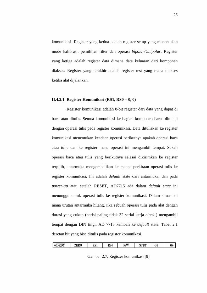
Gambar 2.7 Register Komunikasi..................................................................25
Gambar 2.8 Register Setup.............................................................................28
Gambar 2.9 kaki-kaki IC mikrokontroler ......................................................33
Gambar 2.10 Hubungan ke kristal .................................................................36
Gambar 2.11 Siklus mesin .............................................................................37
Gambar 2.12 Dimensi layar LCD ..................................................................38
Gambar 2.13 Frame character-oriented ........................................................40
Gambar 2.14 Frame bit-oriented ...................................................................40
Gambar 2.15 Rangkaian pembagi tegangan ..................................................42
Gambar 3.1 Diagram blok perancangan ........................................................46
Gambar 3.2 Elemen sensor MPX4100...........................................................37
Gambar 3.3 Perbandingan Vout dengan tekanan udara .................................37
Gambar 3.4 Rangkaian sensor tekanan udara MPX4100 ..............................48
Gambar 3.5 Rangkaian ADC dan sensor MPX4100......................................49
Gambar 3.6 Rangkaian mikrokontroler AT89S53.........................................53
xvii
Gambar 3.7 Gelombang kotak 1 Hz...............................................................54
Gambar 3.8 Antarmuka ADC dan mikrokontroler ........................................55
Gambar 3.9 Antarmuka mikrokontroler dan LCD.........................................59
Gambar 3.10 Rangkaian catu daya ................................................................60
Gambar 3.11. Rangkaian pembagi tegangan .................................................62
Gambar 3.12. Penyearah LPF tipe π................................................................62
Gambar 3.13 Rangkaian Altimeter dan barometer digital .............................63
Gambar 3.14 Diagram alir sistem kerja altimeter dan barometer ..................65
Gambar 3.15 Diagram alir pengambilan dan pengisian untuk ADC .............68
Gambar 3.16 Diagram alir proses konversi data menjadi karakter ASCII ....71
Gambar 4.1 Grafik perbandingan barometer digital terhadap data BMG......79
Gambar 4.2 Grafik perbandingan altimeter digital terhadap data BMG........80
Gambar 4.3 Menu dan sub menu pada alat ukur............................................83
Gambar 4.4 Perbandingan Vout sensor terhadap tekanan udara....................86
Gambar 4.5 Gelombang keluaran pin 1 (SCLK)............................................87
Gambar 4.6 Gelombang keluaran pin 14 (DIN).............................................88
Gambar 4.7 Gelombang keluaran pin 13 (DOUT).........................................88
Gambar 4.8 Bentuk Gelombang SDA............................................................90
Gambar 4.9 Bentuk Gelombang SCL.............................................................90
xviii
DAFTAR TABEL
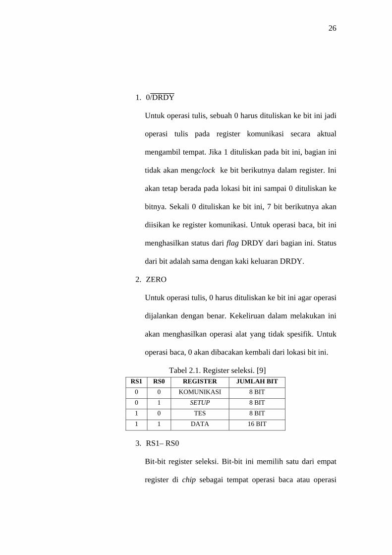
Tabel 2.1 Register seleksi...............................................................................26
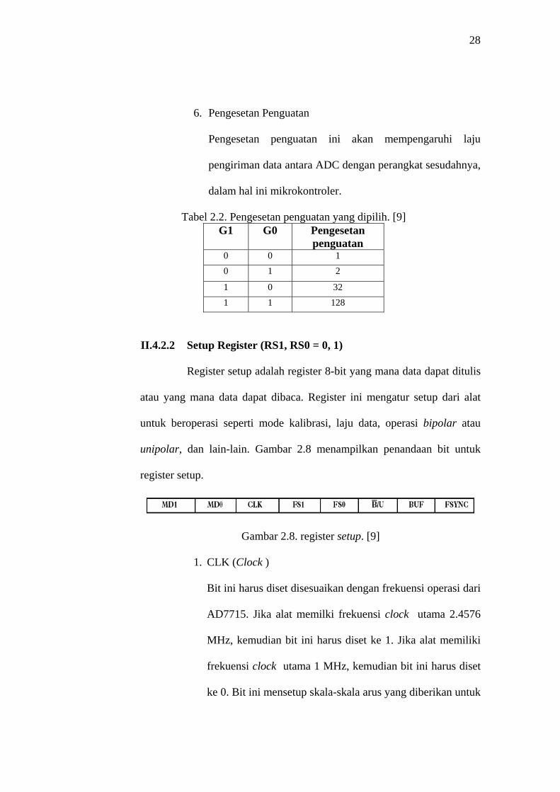
Tabel 2.2. Pengesetan penguatan yangdipilih.................................................28
Tabel 2.3. Mode operasi..................................................................................29
Tabel 2.4. Laju data keluaran..........................................................................30
Tabel 2.5. Fungsi-fungsi khusus kaki port 3..................................................34
Tabel 3.1 Penggunaan Port – port pada mikrokontroler................................52
Tabel 4.1 Data kalibrasi...................................................................................73
Tabel 4.2 Data pengujian alat ukur..................................................................74
Tabel 4.3 Pengukuran pada lokasi dengan ketinggian 100 m.........................74
Tabel 4.4 Perbandingan data dengan masukan nilai kalibrasi yang tepat.......76
Tabel 4.5. Tingkat kesalahan dan deviasi barometer digital...........................77
Tabel 4.6. Tingkat kesalahan dan deviasi altimeter digital.............................78
Tabel 4.7. Tingkat ketelitian altimeter digital.................................................78
Tabel 4.8. Tingkat ketelitian barometer digital...............................................79
Tabel 4.9. Perbandingan Vout sensor..............................................................85
xix
DAFTAR LAMPIRAN
L.1. 16-Bit, Sigma Delta ADC AD7715 Datasheet.
L.2. 8-Bit Microcontroller with 12K Bytes Flash AT89S53 Datasheet.
L.3. Integrated Silicon Pressure Sensor for Manifold Absolute Pressure
Applications On-Chip Signal Conditioned, Temperatured Compesated and
Calibrated MPX4100 Datasheet.
L.4. Dot Matrix Liquid Crystal Display Controller/Driver HD44780U datasheet
L.5 Listing Program altimeter dan barometer digital.
BAB I
PENDAHULUAN
I.1 Judul
Altimeter dan Barometer Digital berbasis AT89S53
I.2 Latar Belakang Masalah.
Umumnya, di dalam pengukuran dibutuhkan suatu instrumen sebagai
suatu cara fisis untuk menentukan suatu besaran (kuantitas) atau variabel.
Instrumen tersebut membantu peningkatan ketrampilan manusia dan dalam
banyak hal memungkinkan seseorang untuk menentukan nilai dari suatu besaran
yang tidak diketahui. Dengan demikian, sebuah instrumen dapat didefinisikan
sebagai sebuah alat yang digunakan untuk menentukan nilai atau besaran dari
suatu kuantitas atau variabel.
Altimeter adalah suatu alat ukur yang digunakan untuk mengukur suatu
ketinggian tempat dari atas permukaan laut. Dengan adanya altimeter ini maka
suatu ketinggian tempat dapat diketahui dengan mudah. Biasanya hasil
pengukuran altimeter dalam satuan meter (menurut standar internasional). Sebuah
altimeter adalah sebuah instrumen aktif digunakan untuk mengukur ketinggian
suatu obyek diatas sebuah level ketinggian yang tetap. Altimeter yang tradisional
ditemukan di banyak pesawat pengangkut (yang biasa disebut altimeter Kollsman
berada di sebelah kanan kokpit pilot) dengan mengevaluasi hasil pengukuran
tekanan udara dari sebuah tempat yang tetap. Tekanan udara menurun dengan
1
2
meningkatnya ketinggian, sekitar 1 milibar (0.03 inci dari raksa) per 27 kaki (8.23
m) dari permukaan laut. Altimeter dikalibrasikan untuk menunjukkan tekanan
secara langsung seperti ketinggian, yang disesuaikan dengan model matematika
oleh ISA (International Standar Atmosphere).[13]
Barometer adalah suatu alat ukur yang digunakan untuk mengukur tekanan
udara di suatu tempat tertentu. Dalam aplikasinya suatu barometer digunakan
untuk memprediksi cuaca beberapa jam mendatang. Biasanya hasil pengukuran
altimeter dalam satuan pascal atau milibar (menurut standar internasional). Salah
satu model barometer kuno adalah aneroid barometer, berukuran kecil,
menggunakan kotak logam yang fleksibel dinamakan aneroid cell. Kotak ini akan
tersegel secara rapat setelah beberapa satuan udara dipindahkan, jadi perubahan
yang sangat kecil pada tekanan udara sekitar akan menyebabkan cell ini berubah
atau berkontraksi. Perubahan dan kontraksi ini akan membuat gerakan mekanik
yang serial dan komponen-komponen lainnya pada aneroid barometer yang
ditampilkan pada aneroid barometer. [14]
Dengan melihat secara mendalam pada aneroid barometer yang biasa
tidak dapat berkata banyak tentang cuaca yang diperkirakan. Yang dapat diketahui
dari barometer aneroid adalah tentang kecepatan, magnitude dan variasi dari arah
angin di tekanan atmosfer. Informasi-informasi ini memberikan suatu perkiraan
yang cukup akurat tentang keadaan cuaca beberapa jam mendatang. Sayangnya
aneroid barometer tidak terlalu akurat dalam memberikan suatu perkiraan
informasi mengenai cuaca, sebuah barometer raksa lebih baik untuk perkiraan
3
cuaca. Akan tetapi barometer raksa tidak mudah untuk dibawa dan sangat sulit
dalam penggunaannya.
Dengan melihat sejarah dan perkembangan dari barometer dan
altimeter dapat disimpulkan bahwa penggunaan dari alat ini sangat terbatas pada
beberapa instansi saja dalam hal ini instansi-instansi penerbangan dan kantor
berita cuaca. Pendataan ketinggian tempat dan tekanan udara biasanya hanya
dapat kita ketahui melalui suatu kantor berita cuaca ataupun instansi-instansi yang
memerlukan data ketinggian tempat dan tekanan udara. Para penggiat alam
biasanya memerlukan data ketinggian tempat dan tekanan udara karena kedua hal
ini nanti erat kaitannya dengan cuaca.
Barometer dan altimeter yang dibuat secara analog ternyata memiliki
kelemahan karena kurang teliti dalam pembacaannya. Garis-garis penunjuk
ketinggian dan tekanan udara yang ditampilkan pada papan penampil memiliki
skala antar garis sebesar 10 m. Jadi kita hanya bisa mengkira-kira level ketinggian
dan tekanan udara jika jarum berada di antara selang garis tersebut. Kelemahan
yang lain adalah kita harus mengkalibrasikan alat ini di tempat yang level
ketinggian atau tekanan udaranya pasti karena jika tidak maka alat tidak dapat
digunakan secara optimal.
Di dalam pengukuran sangatlah dibutuhkan suatu ketelitian, ketepatan,
kepekaan. Hal tersebut dapat dipengaruhi oleh beberapa sebab antara lain
kesalahan karena pembacaan alat ukur (penaksiran), penyetelan yang tidak tepat
dan pemakaian instrumen yang tidak sesuai, kesalahan instrumen (kekurangan-
kekurangan dari instrumen itu sendiri), keadaan-keadaan luar yang
4
mempengaruhi, kesalahan acak (kesalahan diakibatkan oleh penyebab yang tidak
diketahui), dan lain-lain.
Dengan adanya kelemahan-kelemahan di atas maka penting untuk dicoba
meminimalisasi faktor kesalahan dari hal-hal diatas. Dengan menggunakan
teknologi digital maka error faktor, baik dari si pemakai maupun lingkungan
dapat semakin ditekan. Alat yang akan dibuat ini nantinya akan lebih sensitif dan
dirancang agar faktor kesalahan dapat semakin kecil. Dengan menggunakan LCD
(Liquid Cristal Display) sebagi tampilan, maka pembacaan dari besaran
ketinggian maupun tekanan udara dapat semakin meyakinkan. Untuk kalibrasi
secara digital juga tidak terlalu sulit karena pada komponen yang dipilih sudah
ada pilihan rangkaian yang menunjang alat yang akan dibuat untuk melakukan
kalibrasi sendiri.
Dalam kenyataannya barometer dan altimeter dibuat dalam satu paket alat.
Dalam pembuatannya biasanya altimeter dan barometer (baik dengan penunjuk
menggunakan jarum kumparan maupun dengan penampil elektronik)
menggunakan satu sensor yang dapat digunakan untuk mengukur dua variabel
yaitu tekanan udara dan ketinggian tempat.
Dengan berkembangnya teknologi sekarang ini, tuntutan dan kebutuhan
alat ukur yang lebih terpercaya dan lebih teliti semakin meningkat, yang
kemudian menghasilkan perkembangan-perkembangan baru dalam perencanaan
dan pemakaiannya. Salah satunya adalah altimeter dan barometer digital berbasis
AT89S53.
5
Dengan adanya altimeter dan barometer digital ini maka para penggiat
alam bisa langsung mendapatkan informasi yang akurat di lokasi tanpa harus
mendatangi kantor berita cuaca atau instansi-instansi yang berkompeten. Hasil
dari pengukuran ini akan ditampilkan pada sebuah LCD matrik 16x2 baris.
I.3 Tujuan
Tujuan pembuatan alat ini untuk mengukur ketinggian tempat dan tekanan
udara dan ditampilkan pada LCD (Liquid Crystal Display)
I.4 Perumusan Masalah
Dengan melihat tujuan dan latar belakang yang ada, maka permasalahan
yang dapat dirumuskan pada pembuatan alat ini adalah sebagai berikut:
1. Apakah altimeter dan barometer yang dibuat secara digital ini akan
memiliki tingkat ketelitian yang lebih tinggi daripada altimeter dan
barometer yang dibuat secara analog?
2. Apakah pemilihan komponen yang tepat dalam proses perancangan
akan mempengaruhi sensitivitas pengukuran dalam praktek?
3. Bagaimana cara mengkonversikan besaran ketinggian dari besaran
tekanan udara?
I.5 Batasan Masalah
Agar permasalahan yang ada tidak berkembang menjadi luas, maka perlu
adanya batasan terhadap permasalahan yang akan dibuat yaitu:
6
1. Hasil pengukuran ditampilkan pada LCD matrik 2x16 .
2. Nilai ketinggian -2000 m sampai dengan +10.000 m
3. Hasil pengukuran adalah Real time.
4. Satuan tekanan udara dalam hPa dan ketinggian dalam meter.
5. Perbandingan data hasil pengukuran menggunakan data BMG.
6. Sensitivitas pengukuran adalah 54 mV/kPa (jaminan dari sensor
MPX4100 buatan Motorola).
I.6 Manfaat
Adapun manfaat dari pembuatan alat ini adalah :
1. Sebagai alat bantu para penggiat alam dalam memperoleh data
ketinggian tempat dan tekanan udara agar dapat memprediksikan
keadaan cuaca di masa depan dengan lebih akurat..
2. Dapat digunakan untuk mengukur ketinggian relatif dengan
referensi ketinggian tempat yang dipilih secara acak.
3. Dapat digunakan untuk mengukur tekanan udara di berbagai
daerah secara akurat.
4. Sebagai alat bantu dalam instalasi antena atau menara transmisi.
5. Sebagai alat bantu dalam orientasi medan dan navigasi darat.
6. Sebagai alat bantu dalam penelusuran gua (Caving) karena dapat
mengukur sampai dengan -2000 meter.
7
I.7 Metode Penelitian dan Pengambilan Data
Dalam perancangan alat ini, penelitian dilakukan dengan cara melakukan
serangkaian percobaan baik di laboratorium maupun ditempat lain. Pengambilan
data sebagai referensi digunakan barometer analog, altimeter analog, serta
multimeter.
Dalam perancangan suatu alat ukur ada beberapa proses yang harus
dilewati. Adapun proses ini adalah tahapan-tahapan yang harus dilewati. Agar
dalam perancangan dapat maksimal dan ide yang dituangkan sebelumnya dapat
terwujud maka tahapan-tahapan itu adalah:
1. Telaah teori.
Dalam proses telaah teori yang dilakukan adalah
mengumpulkan data dan informasi baik itu dari internet maupun
perpustakaan yang berhubungan dengan alat yang akan dibuat.
Yang nantinya diharapkan dapat membantu dalam proses-proses
selanjutnya.
2. Perancangan software dan hardware
Setelah mendapatkan banyak data dan informasi mengenai
alat ukur yang akan dibuat maka dapat dilanjutkan ke tahap
berikutnya yaitu perancangan software dan hardware. Sebelum
membuat program yang harus dilakukan adalah membuat diagram
alirnya.
8
3. Implementasi software dan hardware
Setelah perancangan software dan hardware selesai maka dapat
dilanjutkan pada tahap selanjutnya yaitu implementasi dari
software dan hardware yang telah dipilih.
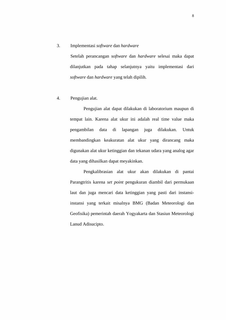
4. Pengujian alat.
Pengujian alat dapat dilakukan di laboratorium maupun di
tempat lain. Karena alat ukur ini adalah real time value maka
pengambilan data di lapangan juga dilakukan. Untuk
membandingkan keakuratan alat ukur yang dirancang maka
digunakan alat ukur ketinggian dan tekanan udara yang analog agar
data yang dihasilkan dapat meyakinkan.
Pengkalibrasian alat ukur akan dilakukan di pantai
Parangtritis karena set point pengukuran diambil dari permukaan
laut dan juga mencari data ketinggian yang pasti dari instansi-
instansi yang terkait misalnya BMG (Badan Meteorologi dan
Geofisika) pemerintah daerah Yogyakarta dan Stasiun Meteorologi
Lanud Adisucipto.
BAB II
DASAR TEORI
II.1 Sistem pengukuran umum
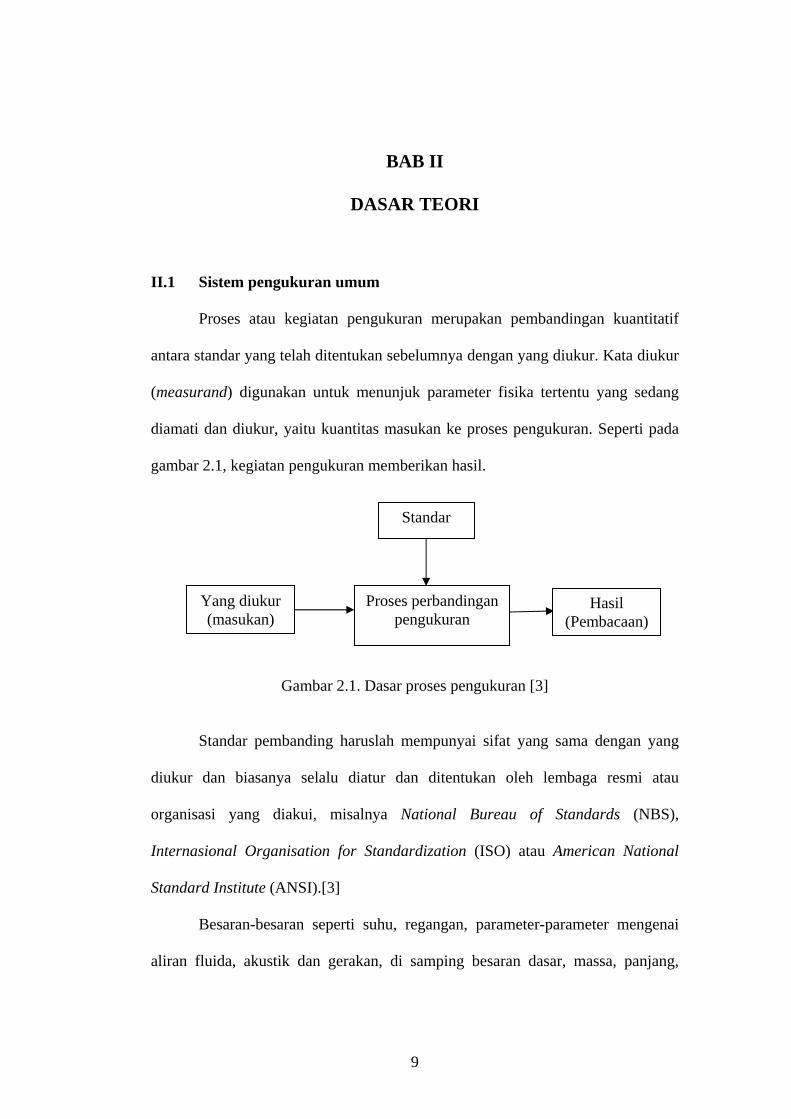
Proses atau kegiatan pengukuran merupakan pembandingan kuantitatif
antara standar yang telah ditentukan sebelumnya dengan yang diukur. Kata diukur
(measurand) digunakan untuk menunjuk parameter fisika tertentu yang sedang
diamati dan diukur, yaitu kuantitas masukan ke proses pengukuran. Seperti pada
gambar 2.1, kegiatan pengukuran memberikan hasil.
Proses perbandingan pengukuran
Standar
Yang diukur (masukan)
Hasil (Pembacaan)
Gambar 2.1. Dasar proses pengukuran [3]
Standar pembanding haruslah mempunyai sifat yang sama dengan yang
diukur dan biasanya selalu diatur dan ditentukan oleh lembaga resmi atau
organisasi yang diakui, misalnya National Bureau of Standards (NBS),
Internasional Organisation for Standardization (ISO) atau American National
Standard Institute (ANSI).[3]
Besaran-besaran seperti suhu, regangan, parameter-parameter mengenai
aliran fluida, akustik dan gerakan, di samping besaran dasar, massa, panjang,
9
10
waktu dan sebagainya, adalah jenis-jenis yang termasuk dalam ruang lingkup
pengukuran. Pengukuran fisis sering mencakup pertimbangan penggunaan alat-
alat listrik karena sering lebih mempermudah untuk mengubah besaran mekanis
yang diukur menjadi besaran listrik yang sesuai.
Terdapat dua macam dasar metode pengukuran:
1. Pembandingan langsung dengan standar primer atau sekunder. Dengan
pembandingan langsung kita membandingkan secara langsung suatu
besaran dengan besaran standar yang berlaku, misalnya pengukuran
panjang suatu batang dengan penggaris atau meteran.
2. Pembandingan tak langsung dengan menggunakan sistem yang telah
dikalibrasi. Pembandingan tak langsung menggunakan beberapa
bentuk alat tranduser yang dikopel dengan alat-alat penghubung, yang
akan kita sebut, secara keseluruhan, sebagai sistem pengukuran.
Rangkaian alat-alat ini mengubah bentuk dasar masukan menjadi
bentuk analogi yang kemudian diproses dan disajikan di bagian
keluran sebagai fungsi masukan yang diketahui. Konversi seperti itu
sering dilakukan agar informasi yang diinginkan dapat dimengerti.
Bantuan suatu sistem diperlukan untuk mengindera, mengubah dan
akhirnya menampilkan keluaran analogi dalam bentuk perpindahan
skala, grafik atau bentuk digital.
Kebanyakan sistem pengukuran mempunyai kerangka kerja yang
pengaturan umumnya terdiri atas 3 tingkat:
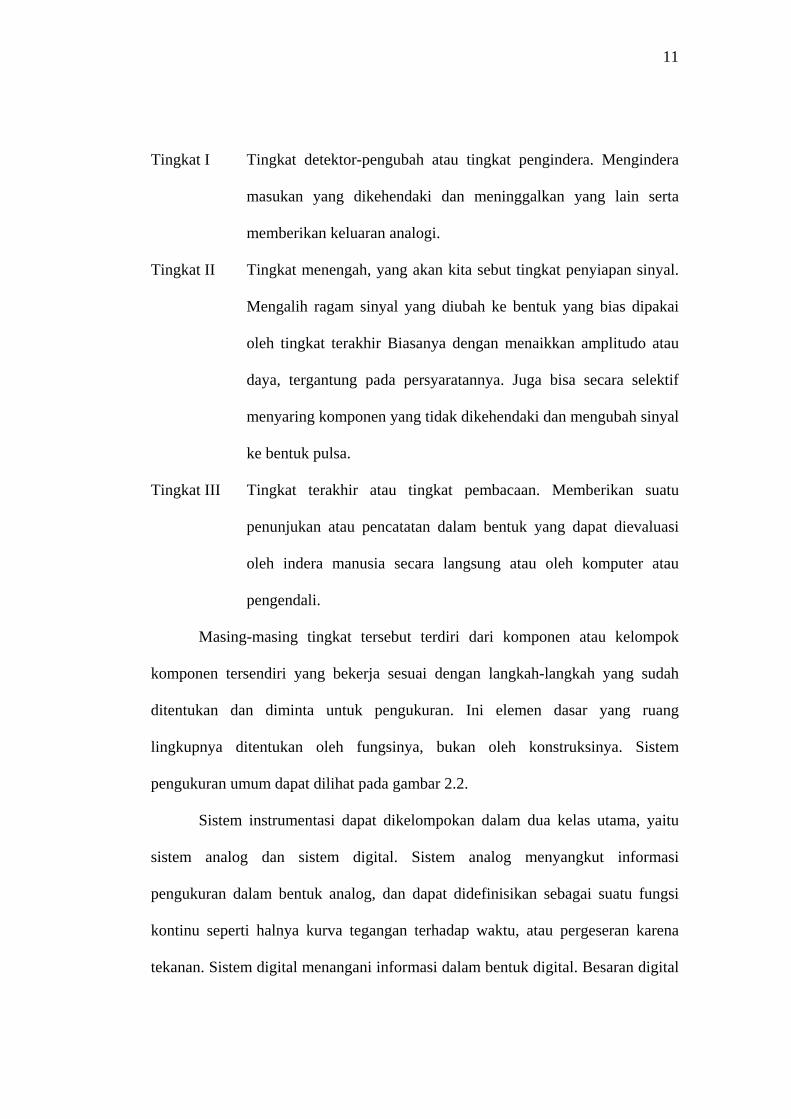
11
Tingkat I Tingkat detektor-pengubah atau tingkat pengindera. Mengindera
masukan yang dikehendaki dan meninggalkan yang lain serta
memberikan keluaran analogi.
Tingkat II Tingkat menengah, yang akan kita sebut tingkat penyiapan sinyal.
Mengalih ragam sinyal yang diubah ke bentuk yang bias dipakai
oleh tingkat terakhir Biasanya dengan menaikkan amplitudo atau
daya, tergantung pada persyaratannya. Juga bisa secara selektif
menyaring komponen yang tidak dikehendaki dan mengubah sinyal
ke bentuk pulsa.
Tingkat III Tingkat terakhir atau tingkat pembacaan. Memberikan suatu
penunjukan atau pencatatan dalam bentuk yang dapat dievaluasi
oleh indera manusia secara langsung atau oleh komputer atau
pengendali.
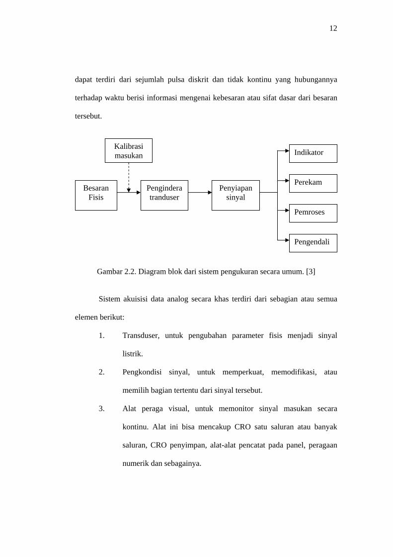
Masing-masing tingkat tersebut terdiri dari komponen atau kelompok
komponen tersendiri yang bekerja sesuai dengan langkah-langkah yang sudah
ditentukan dan diminta untuk pengukuran. Ini elemen dasar yang ruang
lingkupnya ditentukan oleh fungsinya, bukan oleh konstruksinya. Sistem
pengukuran umum dapat dilihat pada gambar 2.2.
Sistem instrumentasi dapat dikelompokan dalam dua kelas utama, yaitu
sistem analog dan sistem digital. Sistem analog menyangkut informasi
pengukuran dalam bentuk analog, dan dapat didefinisikan sebagai suatu fungsi
kontinu seperti halnya kurva tegangan terhadap waktu, atau pergeseran karena
tekanan. Sistem digital menangani informasi dalam bentuk digital. Besaran digital
12
dapat terdiri dari sejumlah pulsa diskrit dan tidak kontinu yang hubungannya
terhadap waktu berisi informasi mengenai kebesaran atau sifat dasar dari besaran
tersebut.
Gambar 2.2. Diagram blok dari sistem pengukuran secara umum. [3]
Sistem akuisisi data analog secara khas terdiri dari sebagian atau semua
elemen berikut:
1. Transduser, untuk pengubahan parameter fisis menjadi sinyal
listrik.
2. Pengkondisi sinyal, untuk memperkuat, memodifikasi, atau
memilih bagian tertentu dari sinyal tersebut.
3. Alat peraga visual, untuk memonitor sinyal masukan secara
kontinu. Alat ini bisa mencakup CRO satu saluran atau banyak
saluran, CRO penyimpan, alat-alat pencatat pada panel, peragaan
numerik dan sebagainya.
Pengindera tranduser
Penyiapan sinyal
Perekam
Indikator
Pemroses
Pengendali
Besaran Fisis
Kalibrasi masukan
13
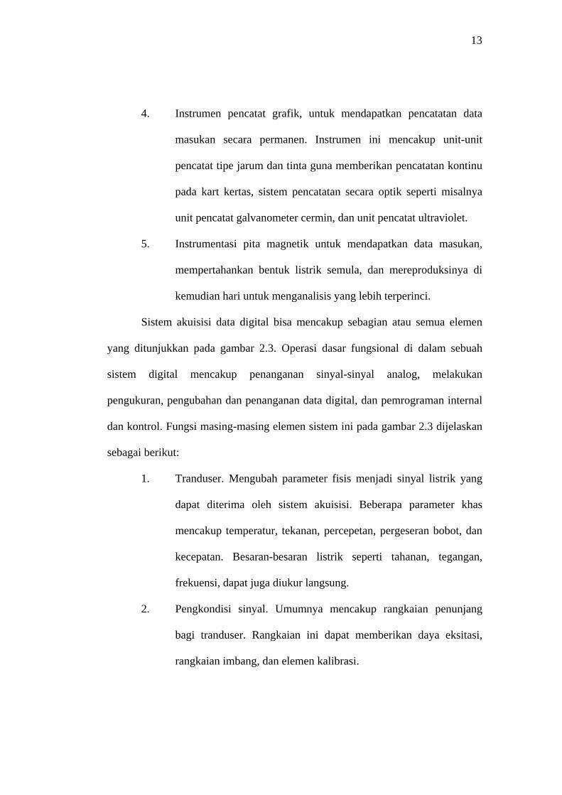
4. Instrumen pencatat grafik, untuk mendapatkan pencatatan data
masukan secara permanen. Instrumen ini mencakup unit-unit
pencatat tipe jarum dan tinta guna memberikan pencatatan kontinu
pada kart kertas, sistem pencatatan secara optik seperti misalnya
unit pencatat galvanometer cermin, dan unit pencatat ultraviolet.
5. Instrumentasi pita magnetik untuk mendapatkan data masukan,
mempertahankan bentuk listrik semula, dan mereproduksinya di
kemudian hari untuk menganalisis yang lebih terperinci.
Sistem akuisisi data digital bisa mencakup sebagian atau semua elemen
yang ditunjukkan pada gambar 2.3. Operasi dasar fungsional di dalam sebuah
sistem digital mencakup penanganan sinyal-sinyal analog, melakukan
pengukuran, pengubahan dan penanganan data digital, dan pemrograman internal
dan kontrol. Fungsi masing-masing elemen sistem ini pada gambar 2.3 dijelaskan
sebagai berikut:
1. Tranduser. Mengubah parameter fisis menjadi sinyal listrik yang
dapat diterima oleh sistem akuisisi. Beberapa parameter khas
mencakup temperatur, tekanan, percepetan, pergeseran bobot, dan
kecepatan. Besaran-besaran listrik seperti tahanan, tegangan,
frekuensi, dapat juga diukur langsung.
2. Pengkondisi sinyal. Umumnya mencakup rangkaian penunjang
bagi tranduser. Rangkaian ini dapat memberikan daya eksitasi,
rangkaian imbang, dan elemen kalibrasi.
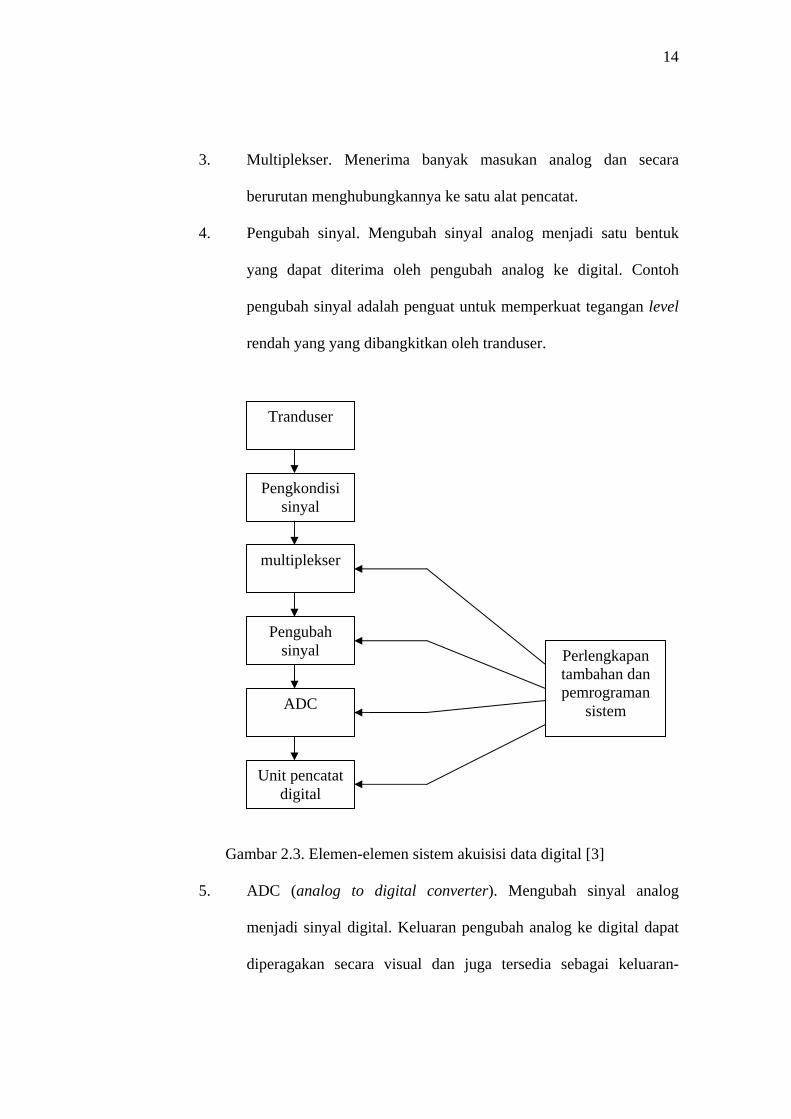
14
3. Multiplekser. Menerima banyak masukan analog dan secara
berurutan menghubungkannya ke satu alat pencatat.
4. Pengubah sinyal. Mengubah sinyal analog menjadi satu bentuk
yang dapat diterima oleh pengubah analog ke digital. Contoh
pengubah sinyal adalah penguat untuk memperkuat tegangan level
rendah yang yang dibangkitkan oleh tranduser.
Tranduser
Pengkondisi sinyal
Pengubah sinyal
Unit pencatat digital
ADC
multiplekser
Perlengkapan tambahan dan pemrograman
sistem
Gambar 2.3. Elemen-elemen sistem akuisisi data digital [3]
5. ADC (analog to digital converter). Mengubah sinyal analog
menjadi sinyal digital. Keluaran pengubah analog ke digital dapat
diperagakan secara visual dan juga tersedia sebagai keluaran-
15
keluaran tegangan dalam tangga diskrit untuk pengolahan
selanjutnya atau untuk pencatatan pada sebuah unit pencatat
digital.
6. Perlengkapan pembantu. Bagian ini berisi instrumen-instrumen
untuk pekerjaan-pekerjaan pemrograman sistem dan pengolahan
data digital. Fungsi khas perlengkapan ini mencakup linearisasi dan
pembandingan batas. Pekerjaan ini dapat dilakukan oleh instrumen
individual atau oleh komputer digital.
7. Unit pencatat digital. Mencatat informasi digital. Unit pencatat
digital dapat didahului oleh sebuah unit penggandeng yang
mengubah informasi digital menjadi bentuk yang sesuai untuk
dimasukkan ke unit pencatat digital yang dipilih secara khusus.
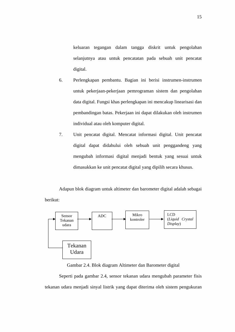
Adapun blok diagram untuk altimeter dan barometer digital adalah sebagai
berikut:
Sensor Tekanan
udara
Tekanan Udara
Mikro kontroler
LCD (Liquid Crystal Display)
ADC
Gambar 2.4. Blok diagram Altimeter dan Barometer digital
Seperti pada gambar 2.4, sensor tekanan udara mengubah parameter fisis
tekanan udara menjadi sinyal listrik yang dapat diterima oleh sistem pengukuran
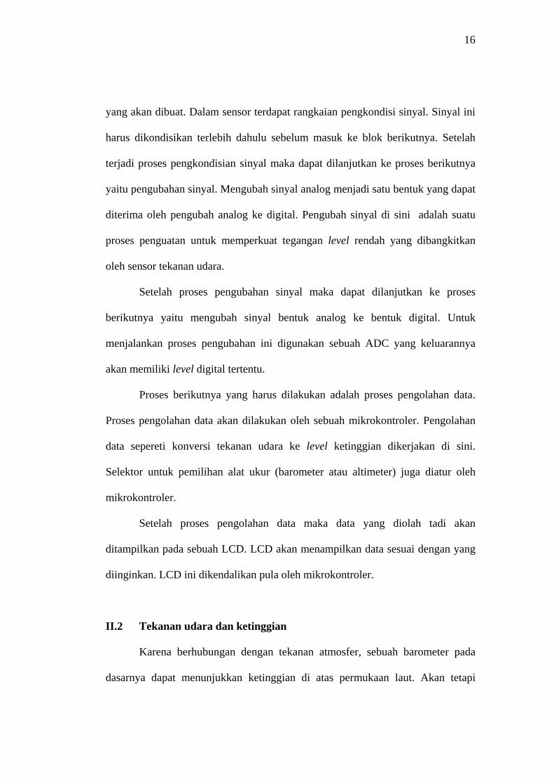
16
yang akan dibuat. Dalam sensor terdapat rangkaian pengkondisi sinyal. Sinyal ini
harus dikondisikan terlebih dahulu sebelum masuk ke blok berikutnya. Setelah
terjadi proses pengkondisian sinyal maka dapat dilanjutkan ke proses berikutnya
yaitu pengubahan sinyal. Mengubah sinyal analog menjadi satu bentuk yang dapat
diterima oleh pengubah analog ke digital. Pengubah sinyal di sini adalah suatu
proses penguatan untuk memperkuat tegangan level rendah yang dibangkitkan
oleh sensor tekanan udara.
Setelah proses pengubahan sinyal maka dapat dilanjutkan ke proses
berikutnya yaitu mengubah sinyal bentuk analog ke bentuk digital. Untuk
menjalankan proses pengubahan ini digunakan sebuah ADC yang keluarannya
akan memiliki level digital tertentu.
Proses berikutnya yang harus dilakukan adalah proses pengolahan data.
Proses pengolahan data akan dilakukan oleh sebuah mikrokontroler. Pengolahan
data sepereti konversi tekanan udara ke level ketinggian dikerjakan di sini.
Selektor untuk pemilihan alat ukur (barometer atau altimeter) juga diatur oleh
mikrokontroler.
Setelah proses pengolahan data maka data yang diolah tadi akan
ditampilkan pada sebuah LCD. LCD akan menampilkan data sesuai dengan yang
diinginkan. LCD ini dikendalikan pula oleh mikrokontroler.
II.2 Tekanan udara dan ketinggian
Karena berhubungan dengan tekanan atmosfer, sebuah barometer pada
dasarnya dapat menunjukkan ketinggian di atas permukaan laut. Akan tetapi
17
dalam hal ini, faktor-faktor lain seperti kelembaban dan suhu juga memberikan
pengaruh. Sayangnya, rancangan sekarang ini tidak dapat memberikan
kompensasi untuk kedua hal ini, kedua hal ini akan membuat masalah menjadi
lebih kompleks. Untuk menggunakan sebuah barometer sebagai altimeter,
membutuhkan sebuah besaran yang berbeda. Hubungan antara tekanan atmosfer
p, pada sebuah ketinggian tempat tertentu h, dan tekanan atmosfer diatas
permukaan laut ps, diberikan pada persamaan 2-1:
⎥⎦
⎤⎢⎣
⎡
Spph = 6
2563.51
10555.22
1
−×
⎥⎦
⎤⎢⎣
⎡−
Spp
(2-1)
Dengan h = ketinggian tempat tertentu (m)
p = tekanan atmosfer (Pa)
ps = tekanan atmosfer dari permukaan laut (Pa)
Sebuah perbedaan harus dibuat antara ketinggian relatif dengan ketinggian
absolut. Suatu ketinggian relatif, hr, direferensikan dengan pemilihan ketinggian
sembarang, ho. Seperti diperlihatakan pada persamaan 2-2:
rh = h ⎥⎦
⎤⎢⎣
⎡
Spp -h ⎥
⎦
⎤⎢⎣
⎡
S
O
pp
(2-2)
Dengan = ketinggian relatif (m) rh
h = ketinggian tempat tertentu (m)
p = tekanan atmosfer (Pa)
ps = tekanan atmosfer dari permukaan laut (Pa)
po = tekanan atmosfer pada h O (Pa)
18
ho = titik referensi ketinggian sembarang (m)
Pengukuran ketinggian relatif hanya bisa dilakukan secara akurat pada saat
tekanan atmosfer di titik referensi ketinggian ada dalam keadaan konstan.
Ketinggian absolut, , direferensikan dari permukaan laut dan
diperhitungkan dengan persamaan 2-3:
ah
ah = h ⎥⎦
⎤⎢⎣
⎡
Spp (2-3)
Dengan ha = ketinggian absolut (m)
h = ketinggian tempat tertentu (m)
p = tekanan atmosfer (Pa)
ps = tekanan atmosfer dari permukaan laut (Pa)
Sejak pengukuran ketinggian absolut tergantung dari tekanan atmosfer
pada level permukaan laut tertentu, maka ps harus secara berkala diperiksa dan
disesuaikan dengan tekanan pada level tertentu ketika alat ukur ingin
dipergunakan.
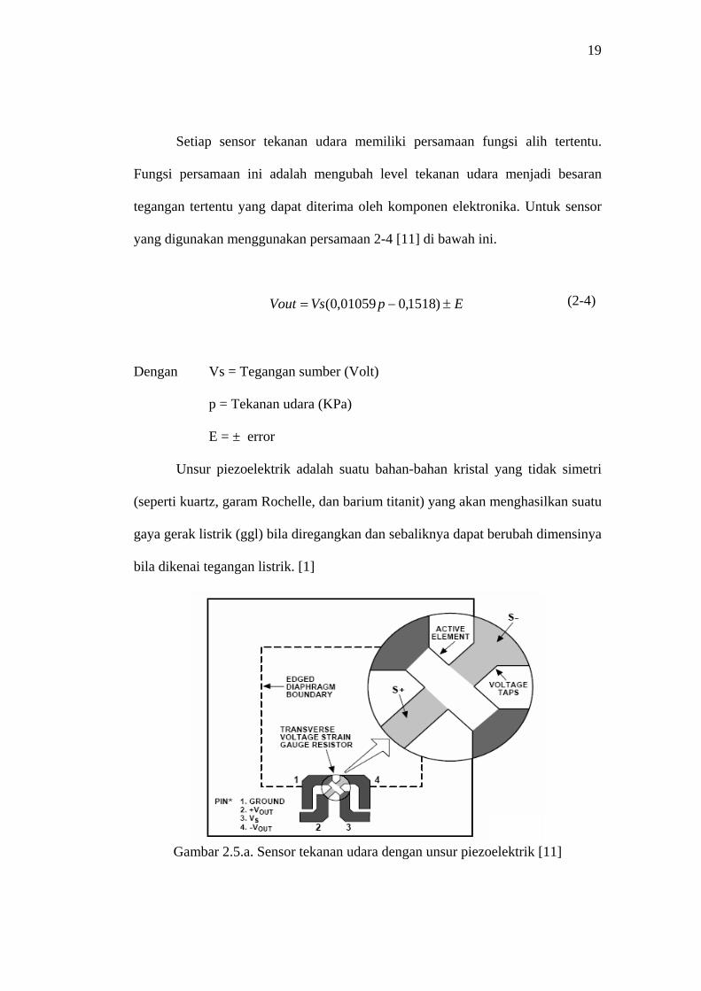
II.3 Sensor Tekanan Udara
Tekanan atmosfer dievaluasi oleh sebuah sensor Tekanan Atmosfer
Absolut (Barometric Absolute Pressure). Sensor berisi sebuah rongga tipis yang
nantinya akan bergeser ke derajat yang lebih tingi bila terkena tekanan udara
seperti terlihat pada gambar 2.5a. Suatu unsur piezoelektrik yang ditunjukan pada
gambar 2.5b, yang dipadukan sepanjang tepi sekat rongga yang ada yang nantinya
akan mengikuti pergerakan sekat rongga tersebut.
19
Setiap sensor tekanan udara memiliki persamaan fungsi alih tertentu.
Fungsi persamaan ini adalah mengubah level tekanan udara menjadi besaran
tegangan tertentu yang dapat diterima oleh komponen elektronika. Untuk sensor
yang digunakan menggunakan persamaan 2-4 [11] di bawah ini.
(2-4) EpVsVout ±−= )1518,001059,0(
Dengan Vs = Tegangan sumber (Volt)
p = Tekanan udara (KPa)
E = ± error
Unsur piezoelektrik adalah suatu bahan-bahan kristal yang tidak simetri
(seperti kuartz, garam Rochelle, dan barium titanit) yang akan menghasilkan suatu
gaya gerak listrik (ggl) bila diregangkan dan sebaliknya dapat berubah dimensinya
bila dikenai tegangan listrik. [1]
Gambar 2.5.a. Sensor tekanan udara dengan unsur piezoelektrik [11]
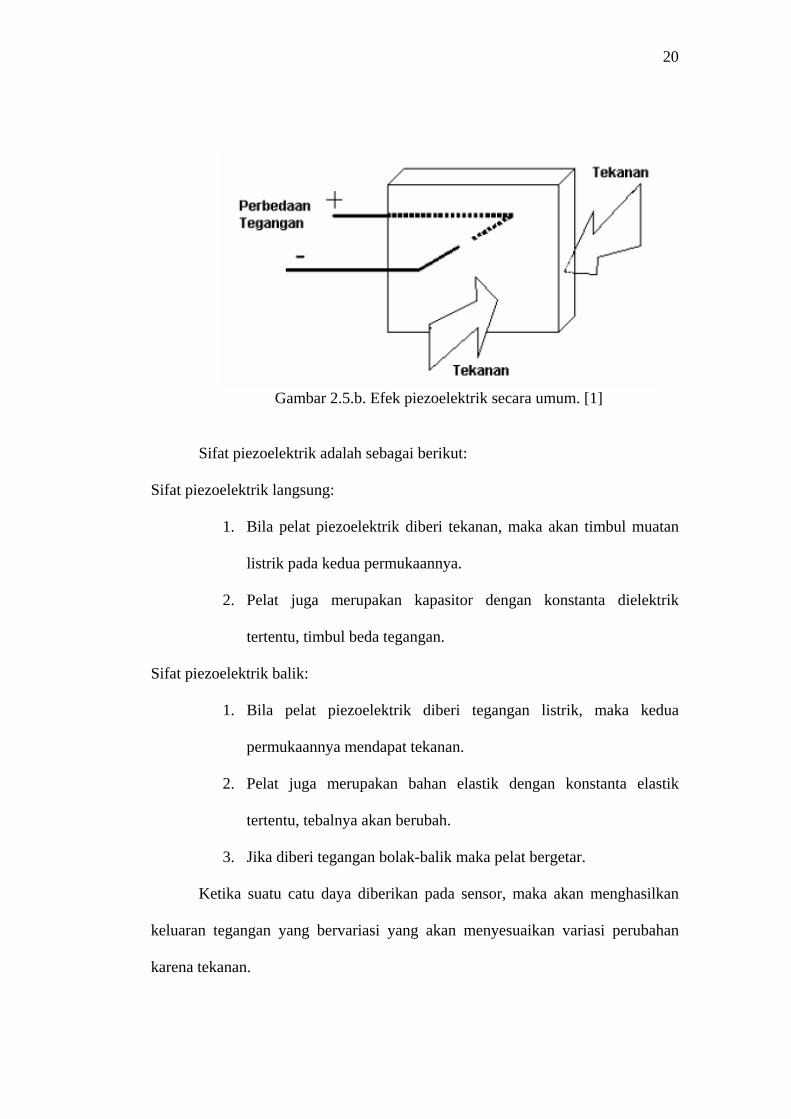
20
Gambar 2.5.b. Efek piezoelektrik secara umum. [1]
Sifat piezoelektrik adalah sebagai berikut:
Sifat piezoelektrik langsung:
1. Bila pelat piezoelektrik diberi tekanan, maka akan timbul muatan
listrik pada kedua permukaannya.
2. Pelat juga merupakan kapasitor dengan konstanta dielektrik
tertentu, timbul beda tegangan.
Sifat piezoelektrik balik:
1. Bila pelat piezoelektrik diberi tegangan listrik, maka kedua
permukaannya mendapat tekanan.
2. Pelat juga merupakan bahan elastik dengan konstanta elastik
tertentu, tebalnya akan berubah.
3. Jika diberi tegangan bolak-balik maka pelat bergetar.
Ketika suatu catu daya diberikan pada sensor, maka akan menghasilkan
keluaran tegangan yang bervariasi yang akan menyesuaikan variasi perubahan
karena tekanan.
21
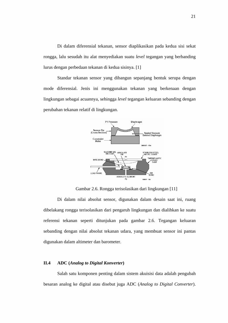
Di dalam diferensial tekanan, sensor diaplikasikan pada kedua sisi sekat
rongga, lalu sesudah itu alat menyediakan suatu level tegangan yang berbanding
lurus dengan perbedaan tekanan di kedua sisinya. [1]
Standar tekanan sensor yang dibangun sepanjang bentuk serupa dengan
mode diferensial. Jenis ini menggunakan tekanan yang berkenaan dengan
lingkungan sebagai acuannya, sehingga level tegangan keluaran sebanding dengan
perubahan tekanan relatif di lingkungan.
Gambar 2.6. Rongga terisolasikan dari lingkungan [11]
Di dalam nilai absolut sensor, digunakan dalam desain saat ini, ruang
dibelakang rongga terisolasikan dari pengaruh lingkungan dan dialihkan ke suatu
referensi tekanan seperti ditunjukan pada gambar 2.6. Tegangan keluaran
sebanding dengan nilai absolut tekanan udara, yang membuat sensor ini pantas
digunakan dalam altimeter dan barometer.
II.4 ADC (Analog to Digital Konverter)
Salah satu komponen penting dalam sistem akuisisi data adalah pengubah
besaran analog ke digital atau disebut juga ADC (Analog to Digital Converter).
22
Pengubah ini akan mengubah besaran-besaran analog menjadi bilangan-bilangan
digital sehingga bisa diproses dengan komputer. Peranan pengubah ini menjadi
semakin penting karena sekarang sudah bisa didapatkan komputer-komputer yang
"real time". Perubahan-perubahan satuan fisis bisa dengan cepat ditanggapi oleh
komputer.
Contoh aplikasi ADC ini bisa kita lihat misalnya pada voltmeter digital, sampling
suara dengan komputer, sehingga suara dapat disimpan secara digital dalam
disket, dan kamera digital.
Konsep pengubah analog ke digital ini adalah sampling (mengambil
contoh dalam waktu tertentu) kemudian mewakilinya dengan bilangan digital
dengan batas yang sudah diberikan.
II.4.1 Parameter ADC
Kuantitas penting dalam ADC adalah rentang tegangan terkecil
yang tidak dapat mengubah hasil konversi. Rentang tegangan ini sering
disebut dengan Minimal Representable Voltage (MRV) atau LSB,
(2-5) MRV = LSB = FS / 2 n
dengan LSB menunjukkan nilai analog dari suatu Least Significant Bit
(LSB), dan FS (Full Scale) adalah nilai maksimum dari tegangan referensi.
Karena semua tegangan dalam jangkauan ini diwakili oleh bilangan biner
yang sama, maka akan terdapat ketidakpastian konversi sebesar ± LSB
untuk setiap pengubahan. Masalah ini dapat dikurangi dengan menambah
jumlah bit pada output pengubah. Output maksimum suatu ADC tidak
23
berada pada nilai FS akan tetapi pada 7/8 FS. Misalkan sebuah ADC 3 bit
ideal, akan mempunyai LSB sebesar 1/8 FS. Jangkauan input akan
dikuantisasikan pada delapan tingkat dari 0 sampai 7/8 kali FS.
Terdapat berbagai cara mengubah sinyal analog ke digital, dalam
pekerjaan ini dipakai metode pendekatan berturutan atau succesive
approximation. Karena ADC dengan jenis ini sudah banyak di pasaran
dalam bentuk chip sehingga mempermudah pemakaian. Metode ini
didasari pada pendekatan sinyal input dengan kode biner dan kemudian
berturut-turut memperbaiki pendekatan ini untuk setiap bit pada kode
sampai didapatkan pendekatan yang paling baik. Untuk meyimpan kode
biner pada setiap tahapan dalam proses digunakan Succesive
Approximation Register (SAR).
Konversi diawali dari most significant bit (MSB) diset tinggi, ini
identik dengan memperkirakan nilai input adalah FS. Komparator akan
membandingkan output DAC (Digital to Analog Converter) dengan
tegangan input dan memerintahkan pengendali untuk mematikan MSB jika
perkiraan mula-mula ternyata lebih besar dari tegangan input. Pada
periode clock selanjutnya pengendali menyalakan MSB berikutnya,
kemudian kembali membandingkan output dari DAC dengan sinyal input.
Proses ini terus diulang sampai pada LSB. Setelah sampai pada tahap ini
nilai konversi yang berada pada SAR adalah pendekatan yang terbaik dari
sinyal input. Dalam proses ini diambil asumsi bahwa sinyal input konstan
selama konversi.
24
Untuk ADC 16 bit dan menggunakan komunikasi serial sinkron maka
dibutuhkan register-register untuk memudahkan komunikasi data antara
mikrokontroler dan ADC. Untuk ADC 16 bit seri AD7715, register-register yang
ada dalam chip dapat diakses oleh mikrokontroler.
II.4.2 Register-register dalam AD7715
Komponen berisi empat register dalam chip yang mana bisa
diakses melalui Port serial dalam komponen. Yang pertama adalah register
komunikasi yang menentukan keadaan operasi apakah operasi baca atau
operasi tulis dan juga menentukan register mana yang mengakses operasi
baca atau tulis. Semua komunikasi pada komponen harus mulai dengan
operasi tulis ke register komunikasi. Setelah power on atau RESET, alat
mengekspresikan operasi tulis ke register komunikasi. Data menuliskan ke
register menentukan operasi berikutnya ke komponen apakah operasi baca
atau tulis dan juga menentukan ke register mana operasi baca atau tulis ini
ditujukan. Bagaimanapun juga, akses tulis ke register yang lain pada
bagian dimulai dengan operasi tulis ke register komunikasi diikuti dengan
tulis ke register yang dipilih. Operasi baca dari register lain dalam
komponen (termasuk register komunikasi itu sendiri dan register data
keluaran) dimulai dengan operasi tulis ke register komunikasi diikuti
dengan operasi baca dari register terpilih. Register komunikasi juga
mengontrol mode standby dan operasi penguatan dari komponen. Status
DRDY (Data Ready) juga tersedia dengan membaca dari register
25
komunikasi. Register yang kedua adalah register setup yang menentukan
mode kalibrasi, pemilihan filter dan operasi bipolar/Unipolar. Register
yang ketiga adalah register data dimana data keluaran dari komponen
diakses. Register yang terakhir adalah register test yang mana diakses
ketika alat dijalankan.
II.4.2.1 Register Komunikasi (RS1, RS0 = 0, 0)
Register komunikasi adalah 8-bit register dari data yang dapat di
baca atau ditulis. Semua komunikasi ke bagian komponen harus dimulai
dengan operasi tulis pada register komunikasi. Data dituliskan ke register
komunikasi menentukan keadaan operasi berikutnya apakah operasi baca
atau tulis dan ke register mana operasi ini mengambil tempat. Sekali
operasi baca atau tulis yang berikutnya selesai dikirimkan ke register
terpilih, antarmuka mengembalikan ke manna perkiraan operasi tulis ke
register komunikasi. Ini adalah default state dari antarmuka, dan pada
power-up atau setelah RESET, AD7715 ada dalam default state ini
menunggu untuk operasi tulis ke register komunikasi. Dalam situasi di
mana urutan antarmuka hilang, jika sebuah operasi tulis pada alat dengan
durasi yang cukup (berisi paling tidak 32 serial kerja clock ) mengambil
tempat dengan DIN tingi, AD 7715 kembali ke default state. Tabel 2.1
deretan bit yang bisa ditulis pada register komunikasi.
Gambar 2.7. Register komunikasi [9]
26
1. 0/DRDY
Untuk operasi tulis, sebuah 0 harus dituliskan ke bit ini jadi
operasi tulis pada register komunikasi secara aktual
mengambil tempat. Jika 1 dituliskan pada bit ini, bagian ini
tidak akan mengclock ke bit berikutnya dalam register. Ini
akan tetap berada pada lokasi bit ini sampai 0 dituliskan ke
bitnya. Sekali 0 dituliskan ke bit ini, 7 bit berikutnya akan
diisikan ke register komunikasi. Untuk operasi baca, bit ini
menghasilkan status dari flag DRDY dari bagian ini. Status
dari bit adalah sama dengan kaki keluaran DRDY.
2. ZERO
Untuk operasi tulis, 0 harus dituliskan ke bit ini agar operasi
dijalankan dengan benar. Kekeliruan dalam melakukan ini
akan menghasilkan operasi alat yang tidak spesifik. Untuk
operasi baca, 0 akan dibacakan kembali dari lokasi bit ini.
Tabel 2.1. Register seleksi. [9] RS1 RS0 REGISTER JUMLAH BIT
0 0 KOMUNIKASI 8 BIT 0 1 SETUP 8 BIT 1 0 TES 8 BIT 1 1 DATA 16 BIT
3. RS1– RS0
Bit-bit register seleksi. Bit-bit ini memilih satu dari empat
register di chip sebagai tempat operasi baca atau operasi
27
tulis berikutnya seperti ditunjukan oleh tabel 2.1 dengan
ukuran registernya juga. Ketika baca atau tulis ke register
terpilih selesai, bagian ini kembali ke tempat semula
menunggu untuk operasi tulis ke register komunikasi. Ini
tidak mengingat keadaan di mana itu akan diteruskan untuk
mengakses register terpilih.
4. R/W
Pemilihan Read/write. Bit ini memilih keadaan dari operasi
berikutnya apakah operasi baca atau tulis ke register yang
dipilih. 0 mengindikasikan kerja tulis sebagai operasi
berikutnya ke register yang terpilih, sementara 1
mengindikasikan operasi baca dari register yang terpilih.
5. STBY (Standby)
Menuliskan 1 ke bit ini meletakan bagian ini pada mode
standby atau power-down. Pada mode ini, bagian hanya
mengkonsumsi 10 mA dari suplai arus. Bagian menahan
kalibrasi dan perintah informasi kontrol ketika itu standby.
Menuliskan 0 ke bit ini meletakan bagian ini pada mode
operasi normal. Nilai default untuk bit ini setelah power-on
atau RESET adalah 0.
28
6. Pengesetan Penguatan
Pengesetan penguatan ini akan mempengaruhi laju
pengiriman data antara ADC dengan perangkat sesudahnya,
dalam hal ini mikrokontroler.
Tabel 2.2. Pengesetan penguatan yang dipilih. [9] G1 G0 Pengesetan
penguatan 0 0 1 0 1 2
1 0 32 1 1 128
II.4.2.2 Setup Register (RS1, RS0 = 0, 1)
Register setup adalah register 8-bit yang mana data dapat ditulis
atau yang mana data dapat dibaca. Register ini mengatur setup dari alat
untuk beroperasi seperti mode kalibrasi, laju data, operasi bipolar atau
unipolar, dan lain-lain. Gambar 2.8 menampilkan penandaan bit untuk
register setup.
Gambar 2.8. register setup. [9]
1. CLK (Clock )
Bit ini harus diset disesuaikan dengan frekuensi operasi dari
AD7715. Jika alat memilki frekuensi clock utama 2.4576
MHz, kemudian bit ini harus diset ke 1. Jika alat memiliki
frekuensi clock utama 1 MHz, kemudian bit ini harus diset
ke 0. Bit ini mensetup skala-skala arus yang diberikan untuk
29
clock utama dan juga untuk memilih rating keluaran data
untuk alat. Jika bit ini tidak diset dengan benar untuk
frekuensi clock utama dari alat, kemudian alat tidak
beroperasi sesuai spesifikasi. Nilai default untuk bit ini
setelah power-on atau RESET adalah 1.
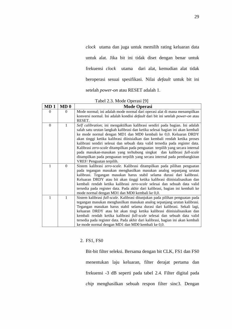
Tabel 2.3. Mode Operasi [9] MD 1 MD 0 Mode Operasi
0 0 Mode normal; ini adalah mode normal dari operasi alat di mana menampilkan konversi normal. Ini adalah kondisi default dari bit ini setelah power-on atau RESET.
0 1 Self calibration; ini mengaktifkan kalibrasi sendiri pada bagian. Ini adalah salah satu urutan langkah kalibrasi dan ketika selesai bagian ini akan kembali ke mode normal dengan MD1 dan MD0 kembali ke 0,0. Keluaran DRDY akan tinggi ketika kalibrasi diinisialkan dan kembali rendah ketika proses kalibrasi sendiri selesai dan sebuah data valid tersedia pada register data. Kalibrasi zero-scale ditampilkan pada penguatan terpilih yang secara internal pada masukan-masukan yang terhubung singkat dan kalibrasi full-scale ditampilkan pada penguatan terpilih yang secara internal pada pembangkitan VREF/ Penguatan terpilih.
1 0 Sistem kalibrasi zero-scale. Kalibrasi ditampilkan pada pilihan penguatan pada tegangan masukan menghasilkan masukan analog sepanjang urutan kalibrasi. Tegangan masukan harus stabil selama durasi dari kalibrasi. Keluaran DRDY atau bit akan tinggi ketika kalibrasi diinisialisasikan dan kembali rendah ketika kalibrasi zero-scale selesai dan sebuah data valid tersedia pada register data. Pada akhir dari kalibrasi, bagian ini kembali ke mode normal dengan MD1 dan MD0 kembali ke 0,0.
1 1 Sistem kalibrasi full-scale. Kalibrasi ditunjukan pada pilihan penguatan pada tegangan masukan menghasilkan masukan analog sepanjang urutan kalibrasi. Tegangan masukan harus stabil selama durasi dari kalibrasi. Sekali lagi, keluaran DRDY atau bit akan tingi ketika kalibrasi diinisialisasikan dan kembali rendah ketika kalibrasi full-scale selesai dan sebuah data valid tersedia pada register data. Pada akhir dari kalibrasi, bagian ini akan kembali ke mode normal dengan MD1 dan MD0 kembali ke 0,0.
2. FS1, FS0
Bit-bit filter seleksi. Bersama dengan bit CLK, FS1 dan FS0
menentukan laju keluaran, filter derajat pertama dan
frekuensi -3 dB seperti pada tabel 2.4. Filter digital pada
chip menghasilkan sebuah respon filter sinc3. Dengan
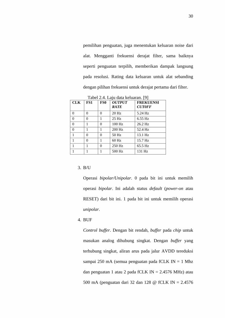
30
pemilihan penguatan, juga menentukan keluaran noise dari
alat. Mengganti frekuensi derajat filter, sama baiknya
seperti penguatan terpilih, memberikan dampak langsung
pada resolusi. Rating data keluaran untuk alat sebanding
dengan pilihan frekuensi untuk derajat pertama dari filter.
Tabel 2.4. Laju data keluaran. [9] CLK FS1 FS0 OUTPUT
RATE FREKUENSI CUT0FF
0 0 0 20 Hz 5.24 Hz 0 0 1 25 Hz 6.55 Hz 0 1 0 100 Hz 26.2 Hz 0 1 1 200 Hz 52.4 Hz 1 0 0 50 Hz 13.1 Hz 1 0 1 60 Hz 15.7 Hz 1 1 0 250 Hz 65.5 Hz 1 1 1 500 Hz 131 Hz
3. B/U
Operasi bipolar/Unipolar. 0 pada bit ini untuk memilih
operasi bipolar. Ini adalah status default (power-on atau
RESET) dari bit ini. 1 pada bit ini untuk memilih operasi
unipolar.
4. BUF
Control buffer. Dengan bit rendah, buffer pada chip untuk
masukan analog dihubung singkat. Dengan buffer yang
terhubung singkat, aliran arus pada jalur AVDD tereduksi
sampai 250 mA (semua penguatan pada fCLK IN = 1 Mhz
dan penguatan 1 atau 2 pada fCLK IN = 2.4576 MHz) atau
500 mA (penguatan dari 32 dan 128 @ fCLK IN = 2.4576
31
MHz) dan keluaran noise dari bagian adalah terendah.
Ketika bit ini tinggi, buffer pada chip adalah serial dengan
masukan analog digunakan untuk mengatasi impedansi
sumber yang tinggi.
5. FSYNC
Sinkronisasi filter. Ketika bit ini tingi, node dari filter
digital, logika filter kontrol dan logika kontrol kalibrasi
ditahan pada keadaan reset dan modulator analog juga
ditahan pada keadaan reset.
II.4.2.3 Test Register (RS1, RS0 = 1, 0)
Bagian ini berisi sebuah register tes yang digunakan untuk
mengetes alat. Pengguna dianjurkan untuk tidak mengubah status dari bit-
bit pada register ini dari semua status default (Power-on atau RESET).
II.4.2.4 Data register Register (RS1, RS0 = 1, 0)
Register data adalah sebuah register 16 bit read-only yang berisi
hasil konversi dari AD 7715. Jika register komunikasi data mengeset
bagian untuk operasi tulis pada register ini, sebuah operasi tulis harus
secara aktual menyediakan tempat untuk mengembalikan bagian di mana
diperintahkan operasi tulis ke register komunikasi.
32
II.5 Mikrokontroler
II.5.1 Pendahuluan
Mikrokontroler adalah salah satu dari bagian dasar dari suatu
sistem komputer. Meskipun mempunyai bentuk yang jauh lebih kecil dari
suatu komputer pribadi dan komputer mainframe, mikrokontroler
dibangun dari elemen-elemen dasar yang sama. Secara sederhana,
komputer akan menghasilkan output spesifik berdasarkan input-an yang
diterima dan program yang dikerjakan.
Seperti umumnya komputer, mikrokontroler adalah alat yang
mengerjakan instruksi-instruksi yang diberikan kepadanya. Artinya,
bagian terpenting dan utama dari suatu sistem terkomputerisasi adalah
program itu sendiri yang dibuat oleh seorang programmer. Program ini
menginstruksikan komputer untuk melakukan jalinan yang panjang dari
aksi-aksi sederhana untuk melakukan tugas yang lebih kompleks yang
diinginkan oleh programmer.
II.5.2 Port Paralel Mikrokontroler
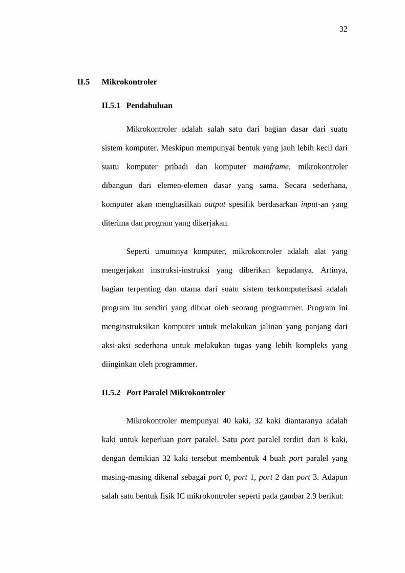
Mikrokontroler mempunyai 40 kaki, 32 kaki diantaranya adalah
kaki untuk keperluan port paralel. Satu port paralel terdiri dari 8 kaki,
dengan demikian 32 kaki tersebut membentuk 4 buah port paralel yang
masing-masing dikenal sebagai port 0, port 1, port 2 dan port 3. Adapun
salah satu bentuk fisik IC mikrokontroler seperti pada gambar 2.9 berikut:
33
91819 29
30
31
12345678
2122232425262728
1011121314151617
3938373635343332
RSTXTAL2XTAL1 PSEN
ALE/PROG
EA/VPP
P1.0P1.1P1.2P1.3P1.4P1.5P1.6P1.7
P2.0/A8P2.1/A9
P2.2/A10P2.3/A11P2.4/A12P2.5/A13P2.6/A14P2.7/A15
P3.0/RXDP3.1/TXD
P3.2/INTOP3.3/INT1
P3.4/TOP3.5/T1
P3.6/WRP3.7/RD
P0.0/AD0P0.1/AD1P0.2/AD2P0.3/AD3P0.4/AD4P0.5/AD5P0.6/AD6P0.7/AD7
Gambar 2.9. Kaki-kaki IC mikrokontroler [4]
1. PORT 0
Port 0 merupakan port keluaran / masukan ( I / O ), yang juga dapat
dikonfigurasikan sebagai bus alamat / data bagian rendah ( low byte )
selama proses pengaksesan memori data dan program eksternal. Selain itu
Port 0 juga menerima kode-kode yang dikirimkan kepadanya selama
proses pemrograman dan mengeluarkan kode-kode selama proses
verifikasi program yang telah tersimpan dalam flash.
2. PORT 1
Port 1 merupakan port keluaran / masukan ( I / O ) dwi-arah yang
dilengkapi dengan pull up internal, dan dapat menerima alamat bagian
rendah ( low byte ) selama pemrograman dan verifikasi flash.
34
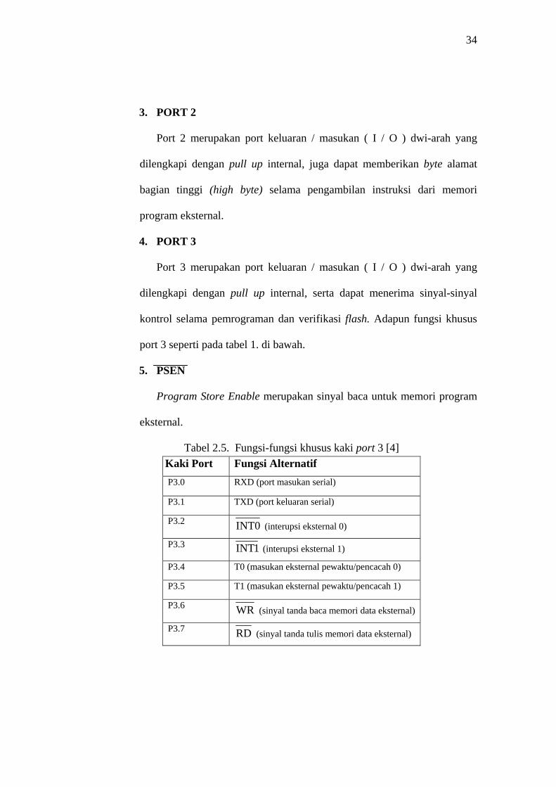
3. PORT 2
Port 2 merupakan port keluaran / masukan ( I / O ) dwi-arah yang
dilengkapi dengan pull up internal, juga dapat memberikan byte alamat
bagian tinggi (high byte) selama pengambilan instruksi dari memori
program eksternal.
4. PORT 3
Port 3 merupakan port keluaran / masukan ( I / O ) dwi-arah yang
dilengkapi dengan pull up internal, serta dapat menerima sinyal-sinyal
kontrol selama pemrograman dan verifikasi flash. Adapun fungsi khusus
port 3 seperti pada tabel 1. di bawah.
5. PSEN
Program Store Enable merupakan sinyal baca untuk memori program
eksternal.
Tabel 2.5. Fungsi-fungsi khusus kaki port 3 [4]
Kaki Port Fungsi Alternatif P3.0 RXD (port masukan serial)
P3.1 TXD (port keluaran serial)
P3.2 0INT (interupsi eksternal 0)
P3.3 1INT (interupsi eksternal 1)
P3.4 T0 (masukan eksternal pewaktu/pencacah 0)
P3.5 T1 (masukan eksternal pewaktu/pencacah 1)
P3.6 WR (sinyal tanda baca memori data eksternal)
P3.7 RD (sinyal tanda tulis memori data eksternal)
35
6. ALE / PROG
Keluaran ALE ( Address Latch Enable ) menghasilkan pulsa-pulsa
yang akan digunakan untuk mengancing byte rendah (low byte) alamat
selama mengakses memori eksternal. Kaki ini juga berfungsi sebagai
masukan pulsa program ( the program pulse input ) selama pemrograman
flash.
7. EA / Vpp
External Access Enable, apabila diberi masukan ‘1’ maka akan
menjalankan program memori internal saja. Tetapi jika diberi masukan ‘0’
maka hanya akan menjalankan program memori eksternal.
8. RST
Merupakan masukan reset, apabila diberi masukan ‘1’ selama dua
siklus mesin pada saat osilator bekerja maka akan mereset mikrokontroler
tersebut
9. XTAL 1 dan XTAL 2
Mikrokontroler telah memiliki on-chip osilator yang dapat bekerja
dengan menggunakan kristal eksternal yang dihubungkan ke kaki XTAL 1
dan XTAL 2.
10. Vcc
Merupakan port yang akan dihubungkan ke suplai tegangan yaitu +5 V
DC.
36
11. GND
Merupakan port yang akan dihubungkan ke ground atau pertanahan.
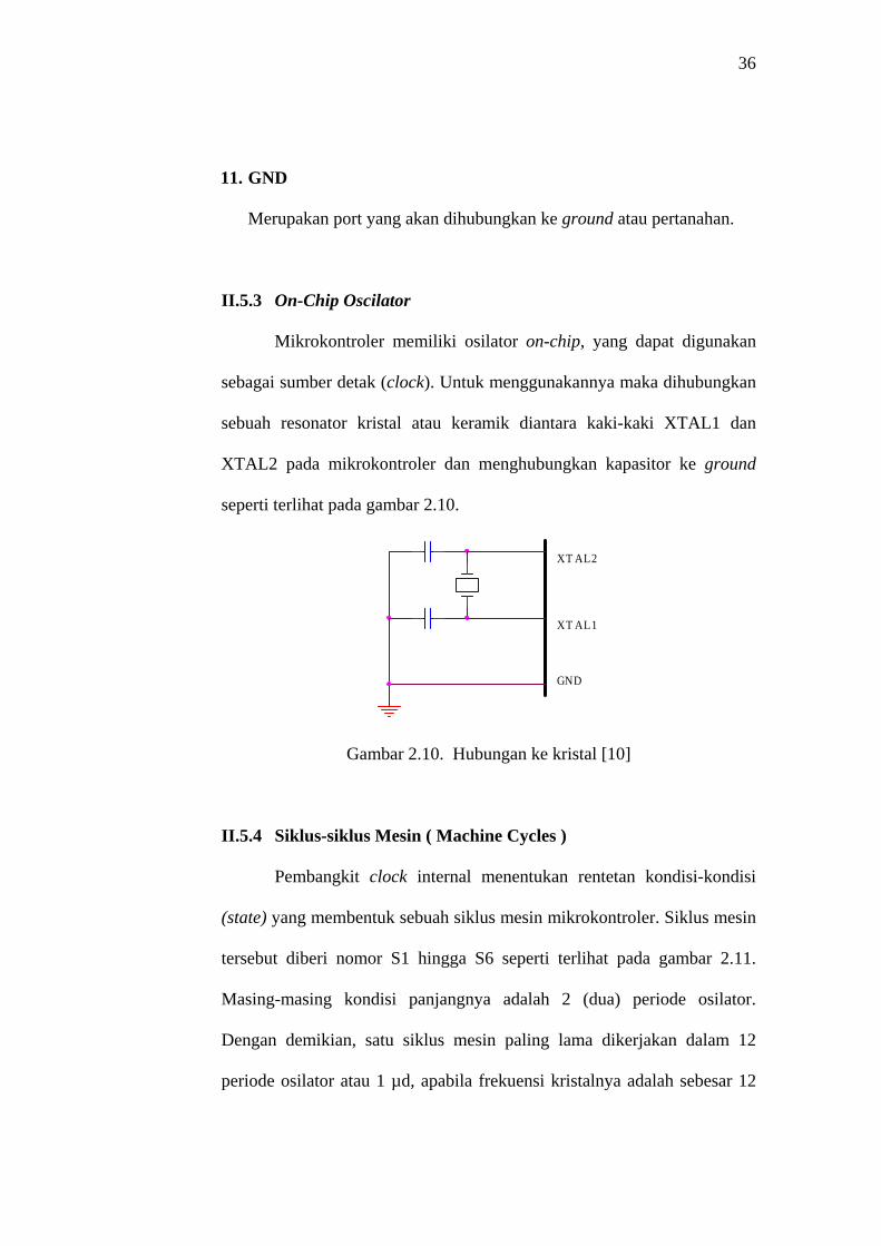
II.5.3 On-Chip Oscilator
Mikrokontroler memiliki osilator on-chip, yang dapat digunakan
sebagai sumber detak (clock). Untuk menggunakannya maka dihubungkan
sebuah resonator kristal atau keramik diantara kaki-kaki XTAL1 dan
XTAL2 pada mikrokontroler dan menghubungkan kapasitor ke ground
seperti terlihat pada gambar 2.10.
XT AL2
XT AL1
GND
Gambar 2.10. Hubungan ke kristal [10]
II.5.4 Siklus-siklus Mesin ( Machine Cycles )
Pembangkit clock internal menentukan rentetan kondisi-kondisi
(state) yang membentuk sebuah siklus mesin mikrokontroler. Siklus mesin
tersebut diberi nomor S1 hingga S6 seperti terlihat pada gambar 2.11.
Masing-masing kondisi panjangnya adalah 2 (dua) periode osilator.
Dengan demikian, satu siklus mesin paling lama dikerjakan dalam 12
periode osilator atau 1 µd, apabila frekuensi kristalnya adalah sebesar 12
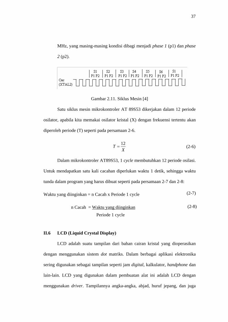
37
MHz, yang masing-masing kondisi dibagi menjadi phase 1 (p1) dan phase
2 (p2).
Gambar 2.11. Siklus Mesin [4]
Satu siklus mesin mikrokontroler AT 89S53 dikerjakan dalam 12 periode
osilator, apabila kita memakai osilator kristal (X) dengan frekuensi tertentu akan
diperoleh periode (T) seperti pada persamaan 2-6.
XT 12=
Dalam mikrokontroler AT89S53, 1 cycle membutuhkan 12 periode osilasi.
Untuk mendapatkan satu kali cacahan diperlukan waktu 1 detik, sehingga waktu
tunda dalam program yang harus dibuat seperti pada persamaan 2-7 dan 2-8:
(2-6)
(2-7) Waktu yang diinginkan = n Cacah x Periode 1 cycle
(2-8) n Cacah = Waktu yang diinginkan
Periode 1 cycle
II.6 LCD (Liquid Crystal Display)
LCD adalah suatu tampilan dari bahan cairan kristal yang dioperasikan
dengan menggunakan sistem dot matriks. Dalam berbagai aplikasi elektronika
sering digunakan sebagai tampilan seperti jam digital, kalkulator, handphone dan
lain-lain. LCD yang digunakan dalam pembuatan alat ini adalah LCD dengan
menggunakan driver. Tampilannya angka-angka, abjad, huruf jepang, dan juga
38
simbol - simbol lainnya. Interface LCD dengan mikrokontroler dapat dilakukan
dengan sistem 4 bit ataupun 8 bit. [12]
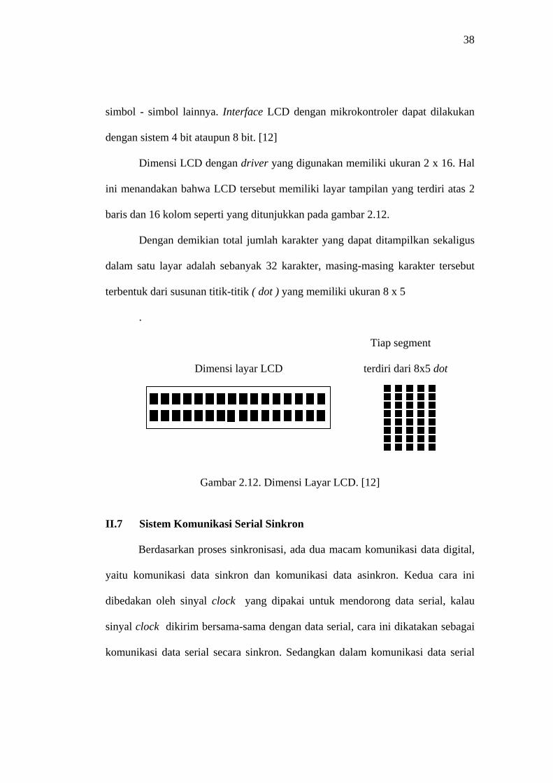
Dimensi LCD dengan driver yang digunakan memiliki ukuran 2 x 16. Hal
ini menandakan bahwa LCD tersebut memiliki layar tampilan yang terdiri atas 2
baris dan 16 kolom seperti yang ditunjukkan pada gambar 2.12.
Dengan demikian total jumlah karakter yang dapat ditampilkan sekaligus
dalam satu layar adalah sebanyak 32 karakter, masing-masing karakter tersebut
terbentuk dari susunan titik-titik ( dot ) yang memiliki ukuran 8 x 5
.
Tiap segment
Dimensi layar LCD terdiri dari 8x5 dot
Gambar 2.12. Dimensi Layar LCD. [12] II.7 Sistem Komunikasi Serial Sinkron
Berdasarkan proses sinkronisasi, ada dua macam komunikasi data digital,
yaitu komunikasi data sinkron dan komunikasi data asinkron. Kedua cara ini
dibedakan oleh sinyal clock yang dipakai untuk mendorong data serial, kalau
sinyal clock dikirim bersama-sama dengan data serial, cara ini dikatakan sebagai
komunikasi data serial secara sinkron. Sedangkan dalam komunikasi data serial
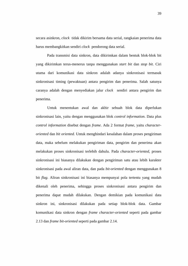
39
secara asinkron, clock tidak dikirim bersama data serial, rangkaian penerima data
harus membangkitkan sendiri clock pendorong data serial.
Pada transmisi data sinkron, data dikirimkan dalam bentuk blok-blok bit
yang dikirimkan terus-menerus tanpa menggunakan start bit dan stop bit. Ciri
utama dari komunikasi data sinkron adalah adanya sinkronisasi termasuk
sinkronisasi timing (pewaktuan) antara pengirim dan penerima. Salah satunya
caranya adalah dengan menyediakan jalur clock sendiri antara pengirim dan
penerima.
Untuk menentukan awal dan akhir sebuah blok data diperlukan
sinkronisasi lain, yaitu dengan menggunakan blok control information. Data plus
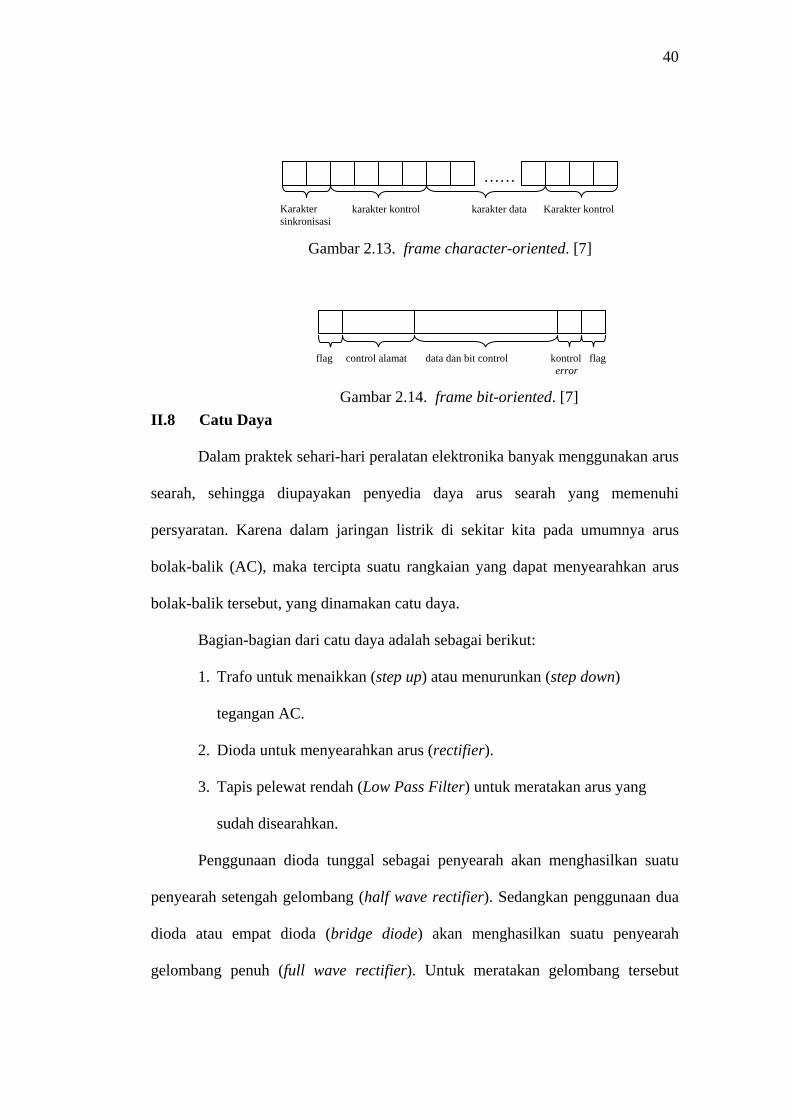
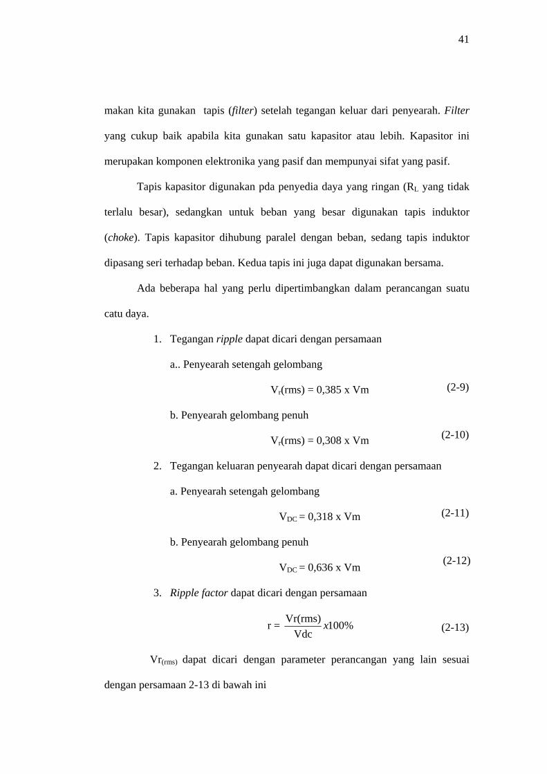
control information disebut dengan frame. Ada 2 format frame, yaitu character-
oriented dan bit oriented. Untuk menghindari kesalahan dalam proses pengiriman
data, maka sebelum melakukan pengiriman data, pengirim dan penerima akan
melakukan proses sinkronisasi terlebih dahulu. Pada character-oriented, proses
sinkronisasi ini biasanya dilakukan dengan pengiriman satu atau lebih karakter
sinkronisasi pada awal aliran data, dan pada bit-oriented dengan menggunakan 8
bit flag. Aliran sinkronisasi ini biasanya mempunyai pola tertentu yang mudah
dikenali oleh penerima, sehingga proses sinkronisasi antara pengirim dan
penerima dapat mudah dilakukan. Dengan demikian pada komunikasi data
sinkron ini, sinkronisasi dilakukan pada setiap blok-blok data. Gambar
komunikasi data sinkron dengan frame character-oriented seperti pada gambar
2.13 dan frame bit-oriented seperti pada gambar 2.14.
40
……
Karakter sinkronisasi
karakter kontrol karakter data Karakter kontrol
Gambar 2.13. frame character-oriented. [7]
Gambar 2.14. frame bit-oriented. [7]
flag control alamat data dan bit control kontrol flag error
II.8 Catu Daya
Dalam praktek sehari-hari peralatan elektronika banyak menggunakan arus
searah, sehingga diupayakan penyedia daya arus searah yang memenuhi
persyaratan. Karena dalam jaringan listrik di sekitar kita pada umumnya arus
bolak-balik (AC), maka tercipta suatu rangkaian yang dapat menyearahkan arus
bolak-balik tersebut, yang dinamakan catu daya.
Bagian-bagian dari catu daya adalah sebagai berikut:
1. Trafo untuk menaikkan (step up) atau menurunkan (step down)
tegangan AC.
2. Dioda untuk menyearahkan arus (rectifier).
3. Tapis pelewat rendah (Low Pass Filter) untuk meratakan arus yang
sudah disearahkan.
Penggunaan dioda tunggal sebagai penyearah akan menghasilkan suatu
penyearah setengah gelombang (half wave rectifier). Sedangkan penggunaan dua
dioda atau empat dioda (bridge diode) akan menghasilkan suatu penyearah
gelombang penuh (full wave rectifier). Untuk meratakan gelombang tersebut
41
makan kita gunakan tapis (filter) setelah tegangan keluar dari penyearah. Filter
yang cukup baik apabila kita gunakan satu kapasitor atau lebih. Kapasitor ini
merupakan komponen elektronika yang pasif dan mempunyai sifat yang pasif.
Tapis kapasitor digunakan pda penyedia daya yang ringan (RL yang tidak
terlalu besar), sedangkan untuk beban yang besar digunakan tapis induktor
(choke). Tapis kapasitor dihubung paralel dengan beban, sedang tapis induktor
dipasang seri terhadap beban. Kedua tapis ini juga dapat digunakan bersama.
Ada beberapa hal yang perlu dipertimbangkan dalam perancangan suatu
catu daya.
1. Tegangan ripple dapat dicari dengan persamaan
a.. Penyearah setengah gelombang
Vr(rms) = 0,385 x Vm
b. Penyearah gelombang penuh
Vr(rms) = 0,308 x Vm
(2-9)
(2-10)
2. Tegangan keluaran penyearah dapat dicari dengan persamaan
a. Penyearah setengah gelombang
VDC = 0,318 x Vm
b. Penyearah gelombang penuh
VDC = 0,636 x Vm
(2-11)
(2-12)
3. Ripple factor dapat dicari dengan persamaan
r = %100Vdc
Vr(rms) x (2-13)
Vr(rms) dapat dicari dengan parameter perancangan yang lain sesuai
dengan persamaan 2-13 di bawah ini
42
Vr(rms) = CR
VdcCIdc
fCIdc
L
4,24,234
== (2-14)
Untuk menghasilkan tegangan keluaran yang stabil dari catu daya dapat
kita gunakan sebuah IC regulator. Besarnya tegangan keluaran yang diinginkan
dapat kita sesuaikan dengan melihat tipe IC regulator yang digunakan.
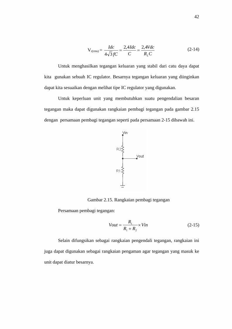
Untuk keperluan unit yang membutuhkan suatu pengendalian besaran
tegangan maka dapat digunakan rangkaian pembagi tegangan pada gambar 2.15
dengan persamaan pembagi tegangan seperti pada persamaan 2-15 dibawah ini.
Gambar 2.15. Rangkaian pembagi tegangan
Persamaan pembagi tegangan:
VinRR
RVout ×+
=21
1 (2-15)
Selain difungsikan sebagai rangkaian pengendali tegangan, rangkaian ini
juga dapat digunakan sebagai rangkaian pengaman agar tegangan yang masuk ke
unit dapat diatur besarnya.
43
II.9 Analisis Statistik
Analisis statistik terhadap data pengukuran merupakan hal yang biasa
sebab ketidakpastian hasil pengujian akhir secara analisis harus ditentukan. Agar
cara-cara statistik dan keterangan yang diberikan bermanfaat, biasanya diperlukan
sejumlah pengukuran yang banyak.
II.9.1 Nilai Rata-rata (Arithmetic Mean)
Nilai yang paling mungkin dari suatu variabel yang diukur adalah
nilai rata-rata dari semua pembacaan yang dilakukan. Pendekatan paling
baik akan diperoleh bila jumlah pembacaan untuk suatu besaran sangat
banyak. Secara teoritis, pembacaan semakin banyak maka hasil paling
baik, walaupun dalam prakteknya hanya dapat dilakukan pengukuran yang
terbatas.
Nilai rata-rata diberikan oleh persamaan :
nnx
nnxxxx
x∑
=++++
=......321 (2-15)
Dengan x = nilai rata-rata
= pembacaan yang dilakukan nxxxx ,,, 321
n = jumlah pembacaan
44
II.9.2 Penyimpangan terhadap nilai rata-rata
Penyimpangan (deviasi) adalah selisih antara suatu pembacaan
terhadap nilai rata-rata dalam sekelompok pembacaan. Jika penyimpangan
pembacaan pertama x1adalah d1, penyimpangan kedua x2 adalah d2 dan
seterusnya, maka penyimpangan-penyimpangan terhadap nilai rata-rata
adalah
d1 = x1 – x d2 = x2 – x dn = xn - x (2-16)
Perlu dicatat bahwa penyimpangan terhadap nilai rata-rata boleh
positif atau negatif dan jumlah aljabar semua penyimpangan tersebut harus
nol.
II.9.3 Perhitungan Tingkat kesalahan
Perhitungan tingkat kesalahan mempunyai tujuan untuk
mengetahui besarnya nilai error dalam persen untuk nilai pengukuran
yang dilakukan dengan alat yang dibuat. Perhitungan error sesuai dengan
persamaan di bawah ini:
%100×⎟⎟
⎠
⎞
⎜⎜
⎝
⎛ −=
xyx
E (2-17)
Dengan x adalah data acuan yang telah ada sebelumnya dan y
adalah data hasil pengukuran. Besarnya error suatu alat ukur yang baik
adalah 0% dimana alat ukur tidak memiliki tingkat kesalahan dan berarti
alat ukur yang dibuat sangat presisi.
45
II.9.4 Perhitungan tingkat keakurasian alat ukur
Perhitungan tingkat keakurasian alat ukur mempunyai tujuan untuk
mengetahui besarnya tingkat akurasi dalam persen untuk nilai pengukuran
yang dilakukan dengan alat yang dibuat. Perhitungan tingkat akurasi
sesuai dengan persamaan di bawah ini:
%1001 ×⎟⎟⎠
⎞⎜⎜⎝
⎛ −−=
xxy
A (2-18)
Dengan x adalah data acuan yang telah ada sebelumnya dan y
adalah data hasil pengukuran. Besarnya tingkat keakurasian suatu alat ukur
yang baik adalah 100% berarti alat ukur yang dibuat sangat presisi.
BAB III
PERANCANGAN
III.1 Diagram Blok
Gambar 3.1 menunjukkan diagram blok perancangan altimeter dan
barometer digital berbasis mikrokontroler AT89S53.
SENSOR MPX4100
ADC AD7715
LCD HITACHI
μC AT89S53
Tekanan Udara
Gambar 3.1. Diagram blok perancangan.
III.2 Sensor tekanan udara (MPX4100)
Sensor menyediakan level tegangan keluaran sebesar 0.3 - 4.9 volt, di
mana tegangan keluaran ini berbanding lurus dengan suatu cakupan tekanan udara
20 – 105 kPa (200 – 105 milibar). Ini hanya memilki galat error sebesar 1.8%
pada cakupan temperature 0 – 85 ° C. sensor ini dapat beroperasi pada suhu
terendah -40 ° C dan suhu tertinggi 125 ° C. Sensor ini juga dapat bertahan pada
tekanan 400 kPa secara kontinyu dan tekanan 1000 kPa sekali lonjakan. [11]
Pada elemen sensor seperti pada gambar 3.2, juga terdapat rangkaian
untuk mengkompensasi perubahan suhu, dua penguat, dan rangkaian penggeser
yang mengubah nilai diferensial suatu pengukuran potensial ke suatu nilai
46
47
referensi tertentu terhadap ground. Sama seperti diatas, sensor menghasilkan
sinyal keluaran yang linear diatas cakupan tekanan udara antara 20 – 105 kPa
dengan sensitivitas 54 mV/kPa yang ditunjukan oleh gambar 3.3.
Gambar 3.2 elemen sensor MPX4100 [11]
Gambar 3.3 Perbandingan Vout dengan tekanan udara [11]
Dengan menggunakan persamaan 2-4 dapat kita tentukan:
• Vout minimum sensor = 1,3427 V
(P = 39,6921 KPa dan sebanding dengan ketinggian 8000m)
• Vout maksimum sensor = 4,3217 V
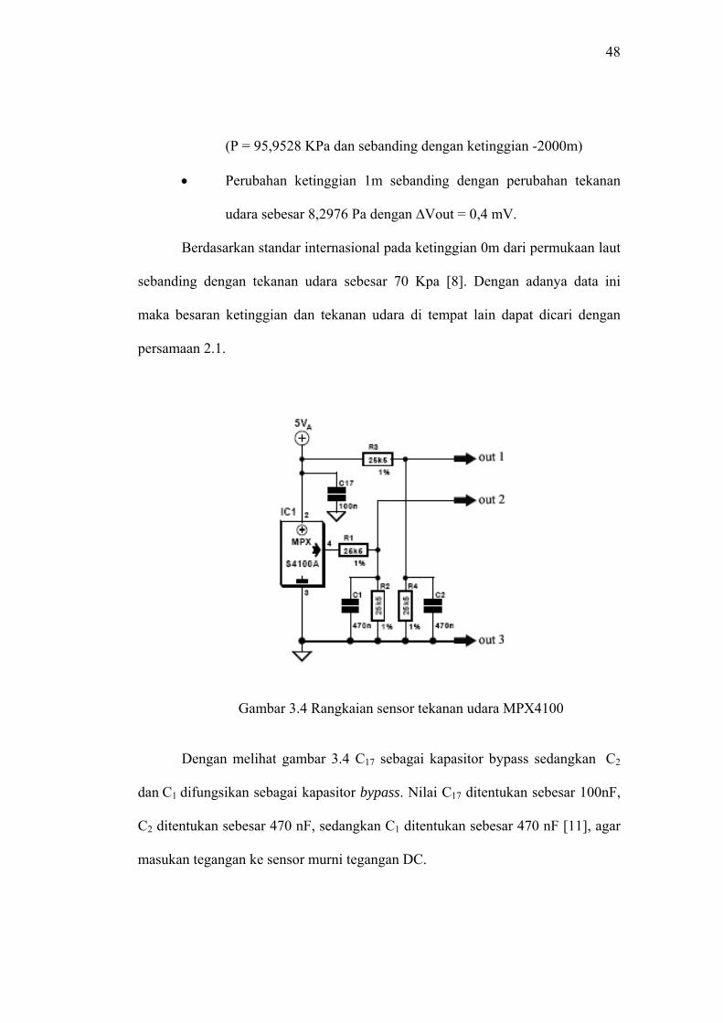
48
(P = 95,9528 KPa dan sebanding dengan ketinggian -2000m)
• Perubahan ketinggian 1m sebanding dengan perubahan tekanan
udara sebesar 8,2976 Pa dengan ∆Vout = 0,4 mV.
Berdasarkan standar internasional pada ketinggian 0m dari permukaan laut
sebanding dengan tekanan udara sebesar 70 Kpa [8]. Dengan adanya data ini
maka besaran ketinggian dan tekanan udara di tempat lain dapat dicari dengan
persamaan 2.1.
Gambar 3.4 Rangkaian sensor tekanan udara MPX4100
Dengan melihat gambar 3.4 C17 sebagai kapasitor bypass sedangkan C2
dan C1 difungsikan sebagai kapasitor bypass. Nilai C17 ditentukan sebesar 100nF,
C2 ditentukan sebesar 470 nF, sedangkan C1 ditentukan sebesar 470 nF [11], agar
masukan tegangan ke sensor murni tegangan DC.
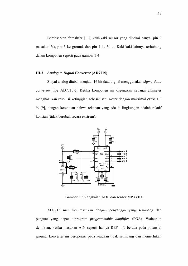
49
Berdasarkan datasheet [11], kaki-kaki sensor yang dipakai hanya, pin 2
masukan Vs, pin 3 ke ground, dan pin 4 ke Vout. Kaki-kaki lainnya terhubung
dalam komponen seperti pada gambar 3.4
III.3 Analog to Digital Converter (AD7715)
Sinyal analog diubah menjadi 16 bit data digital menggunakan sigma-delta
converter tipe AD7715-5. Ketika komponen ini digunakan sebagai altimeter
menghasilkan resolusi ketinggian sebesar satu meter dengan maksimal error 1.8
% [9], dengan ketentuan bahwa tekanan yang ada di lingkungan adalah relatif
konstan (tidak berubah secara ekstrem).
Gambar 3.5 Rangkaian ADC dan sensor MPX4100
AD7715 memiliki masukan dengan penyangga yang seimbang dan
penguat yang dapat diprogram programmable amplifier (PGA). Walaupun
demikian, ketika masukan AIN seperti halnya REF –IN berada pada potensial
ground, konverter ini beroperasi pada keadaan tidak seimbang dan memerlukan
50
sinyal masukan sebesar 0 – 2,5 V (ketika penguatan dari PGA adalah “1”).
Susunan ini memerlukan dua pembagi tegangan antara sensor dengan konverter
untuk membelah tegangan masukan dengan menggunakan persaman 2-14 (R1-
R2) dan tegangan referensi (R3-R4). Tegangan-tegangan ini nantinya akan
dikopling oleh kapasitor C1 dan C2.
Untuk IC AD7715 memerlukan dua tegangan catuan yaitu Catuan analog
(AVDD) dan Catuan digital (DVDD). [9]. Berdasarkan gambar 3.5 maka besarnya
tegangan masukan yang masuk ke AIN+ dan REF+ yang dirancang adalah:
VAIN+ = 0.5 x Vout sensor VREF+ = 0.5 x Vanalog
Besarnya perbandingan R1 dan R2 yang diinginkan adalah 0.5, jika ditentukan
besarnya R1 = 25,5 KΩ maka besarnya R2 = 25,5 KΩ
Vkk
kVAIN 3427,15,255,25
5,25min ×Ω+Ω
Ω=
VAIN min = 0,67135 V
Vkk
kVAIN 3217,45,255,25
5,25max ×Ω+Ω
Ω=
VAIN max = 2,16085 V
Dengan melihat dari data sheet AD7715 maka dapat disimpulkan bahwa
tegangan masukan ke ADC masih dalam rentangan yang diperbolehkan oleh
komponen AD7715 dan komponen akan aman seandainya terjadi lonjakan
tegangan keluaran sensor karena sudah ada resistor pembagi tegangan untuk
mengamankan.
Besarnya perbandingan R3 dan R4 yang diinginkan adalah 0.5, jika
ditentukan besarnya R3 = 25,5 KΩ maka besarnya R2 = 25,5 KΩ
51
log55,255,25
5,25 Vanakk
kVref ×Ω+Ω
Ω=+
VREF+ = 2.5 V
Sebuah kapasitor 1 pF atau yang bernilai lebih besar dibutuhkan antara
output dan ground umtuk menjaga stabilitas tegangan keluran sebesar 5 V. tanpa
adanya kapasitor ini keluaran akan berosilasi. Dengan memperhatikan hal ini
maka dalam perancangan dipilih nilai C yang lebih besar dari 1pF. Adapun
kapasitor yang dimaksud adalah C12 dan C18. Besarnya C12 dan C18 dipilih 100nF.
Osilator utama untuk AD7715 dihasilkan oleh kristal/resonator.
Komponen dispesifikasikan dengan frekuensi clock maksimum masukan sebesar
2.4576 MHz. Clock ini yang menentukan kecepatan transfer datanya. Dalam
sistem altimeter dan barometer ini ADC 16 bit yang digunakan dikendalikan oleh
sebuah Port paralel mikrokontroler AT89S53. Untuk nilai kapasitor kristal C3 dan
C4 dipilih nilai kapasitor sebesar 22 pF karena berdasarkan data sheet rentangan
nilai kapasitor yang diperbolehkan adalah sebesar 20 pF sampai 50 pF [9].
Dengan memilih nilai kapasitor yang berada dalam rentangan ini maka tidak
membutuhkan arus yang berlebihan dari sumber catuan tegangan digital DVDD.
Masukan berupa sinyal analog dan tegangan acuan diaplikasikan pada
suatu sigma-delta modulator, yang nantinya diakhiri ke dalam suatu filter digital.
Keluaran yang digital, DOUT, tersedia dalam bentuk serial, dengan begitu
memudahkan koneksi dengan suatu mikrokontroler. Konverter menyediakan
pengontrol dengan berbagai fasilitas untuk mempengaruhi keseluruhan operasi.
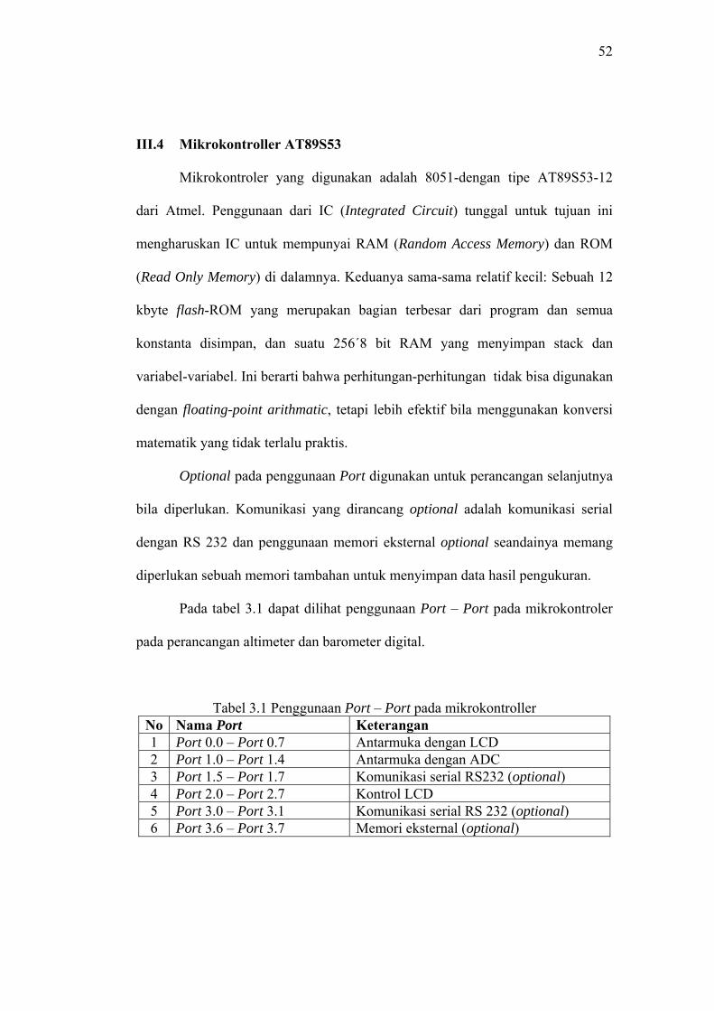
52
III.4 Mikrokontroller AT89S53
Mikrokontroler yang digunakan adalah 8051-dengan tipe AT89S53-12
dari Atmel. Penggunaan dari IC (Integrated Circuit) tunggal untuk tujuan ini
mengharuskan IC untuk mempunyai RAM (Random Access Memory) dan ROM
(Read Only Memory) di dalamnya. Keduanya sama-sama relatif kecil: Sebuah 12
kbyte flash-ROM yang merupakan bagian terbesar dari program dan semua
konstanta disimpan, dan suatu 256´8 bit RAM yang menyimpan stack dan
variabel-variabel. Ini berarti bahwa perhitungan-perhitungan tidak bisa digunakan
dengan floating-point arithmatic, tetapi lebih efektif bila menggunakan konversi
matematik yang tidak terlalu praktis.
Optional pada penggunaan Port digunakan untuk perancangan selanjutnya
bila diperlukan. Komunikasi yang dirancang optional adalah komunikasi serial
dengan RS 232 dan penggunaan memori eksternal optional seandainya memang
diperlukan sebuah memori tambahan untuk menyimpan data hasil pengukuran.
Pada tabel 3.1 dapat dilihat penggunaan Port – Port pada mikrokontroler
pada perancangan altimeter dan barometer digital.
Tabel 3.1 Penggunaan Port – Port pada mikrokontroller No Nama Port Keterangan 1 Port 0.0 – Port 0.7 Antarmuka dengan LCD 2 Port 1.0 – Port 1.4 Antarmuka dengan ADC 3 Port 1.5 – Port 1.7 Komunikasi serial RS232 (optional) 4 Port 2.0 – Port 2.7 Kontrol LCD 5 Port 3.0 – Port 3.1 Komunikasi serial RS 232 (optional) 6 Port 3.6 – Port 3.7 Memori eksternal (optional)
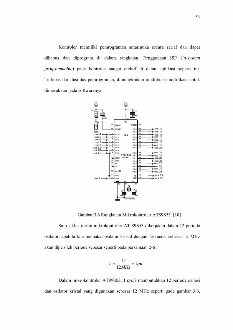
53
Kontroler memiliki pemrograman antarmuka secara serial dan dapat
dihapus dan diprogram di dalam rangkaian. Penggunaan ISP (in-system
programmable) pada kontroler sangat efektif di dalam aplikasi seperti ini.
Terlepas dari fasilitas pemrograman, dimungkinkan modifikasi-modifikasi untuk
dimasukkan pada softwarenya.
Gambar 3.6 Rangkaian Mikrokontroler AT89S53. [10]
Satu siklus mesin mikrokontroler AT 89S53 dikerjakan dalam 12 periode
osilator, apabila kita memakai osilator kristal dengan frekuensi sebesar 12 MHz
akan diperoleh periode sebesar seperti pada persamaan 2-6 :
dMHz
T μ112
12==
Dalam mikrokontroler AT89S53, 1 cycle membutuhkan 12 periode osilasi
dan osilator kristal yang digunakan sebesar 12 MHz seperti pada gambar 3.6,
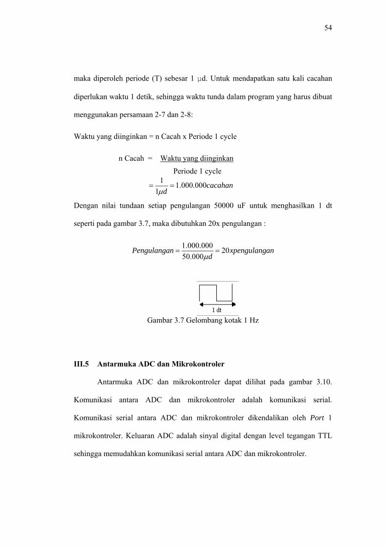
54
maka diperoleh periode (T) sebesar 1 µd. Untuk mendapatkan satu kali cacahan
diperlukan waktu 1 detik, sehingga waktu tunda dalam program yang harus dibuat
menggunakan persamaan 2-7 dan 2-8:
Waktu yang diinginkan = n Cacah x Periode 1 cycle
n Cacah = Waktu yang diinginkan
Periode 1 cycle
cacahand
000.000.11
1==
μ
Dengan nilai tundaan setiap pengulangan 50000 uF untuk menghasilkan 1 dt
seperti pada gambar 3.7, maka dibutuhkan 20x pengulangan :
anxpengulangd
nPengulanga 20000.50
000.000.1==
μ
Gambar 3.7 Gelombang kotak 1 Hz
III.5 Antarmuka ADC dan Mikrokontroler
Antarmuka ADC dan mikrokontroler dapat dilihat pada gambar 3.10.
Komunikasi antara ADC dan mikrokontroler adalah komunikasi serial.
Komunikasi serial antara ADC dan mikrokontroler dikendalikan oleh Port 1
mikrokontroler. Keluaran ADC adalah sinyal digital dengan level tegangan TTL
sehingga memudahkan komunikasi serial antara ADC dan mikrokontroler.
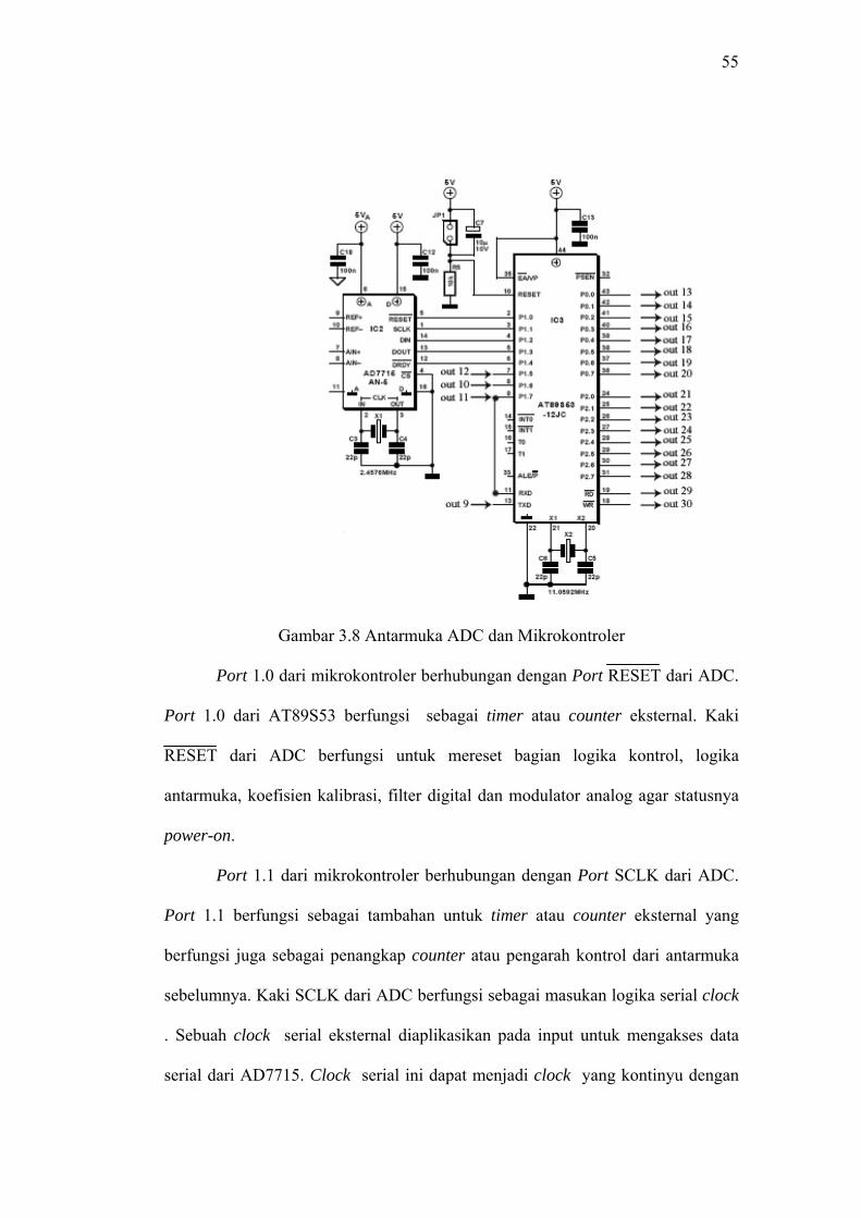
55
Gambar 3.8 Antarmuka ADC dan Mikrokontroler
Port 1.0 dari mikrokontroler berhubungan dengan Port RESET dari ADC.
Port 1.0 dari AT89S53 berfungsi sebagai timer atau counter eksternal. Kaki
RESET dari ADC berfungsi untuk mereset bagian logika kontrol, logika
antarmuka, koefisien kalibrasi, filter digital dan modulator analog agar statusnya
power-on.
Port 1.1 dari mikrokontroler berhubungan dengan Port SCLK dari ADC.
Port 1.1 berfungsi sebagai tambahan untuk timer atau counter eksternal yang
berfungsi juga sebagai penangkap counter atau pengarah kontrol dari antarmuka
sebelumnya. Kaki SCLK dari ADC berfungsi sebagai masukan logika serial clock
. Sebuah clock serial eksternal diaplikasikan pada input untuk mengakses data
serial dari AD7715. Clock serial ini dapat menjadi clock yang kontinyu dengan
56
data transmisi dalam deretan pulsa-pulsa yang kontinyu. Dapat dikatakan ini
menjadi clock yang tidak kontinyu dengan informasi yang ditransmisikan ke
AD7715 dalam sekumpulan data yang lebih kecil.
Port 1.2 mikrokontroler berfungsi untuk input data DIN dari
mikrokontroler ke ADC. Port 1.3 mikrokontroler berfungsi untuk input data ke
mikrokontroler dari DOUT ADC. Kaki DOUT adalah kaki keluaran data serial
dengan data serial dibaca dari bagian keluaran register geser. Keluaran register
geser dapat berisi informasi dari register setup, register komunikasi atau register
data tergantung dari bit-bit register seleksi dari register komunikasi. Sedangkan
DIN adalah masukan data serial dengan data serial dituliskan ke bagian register
geser. Data dari masukan register geser ditransfer ke register setup atau register
komunikasi tergantung dari bit-bit register seleksi dari register komunikasi.
Port 1.4 mikrokontroler adalah Port slave yang berfungsi untuk memilih
input mikrokontroler. Kaki DRDY berhubungan dengan Port ini. Kaki DRDY
pada ADC adalah sebuah logika keluaran. Sebuah logika rendah pada keluaran
mengindikasikan bahwa perintah keluaran yang baru didapatkan dari register data
AD 7715. Kaki DRDY akan kembali tinggi ketika pembacaan dari register data
telah selesai. Jika tidak pembacaan data mengambil tempat antara pembaharuan
keluaran, sementara DRDY tinggi, operasi baca tidak boleh dicoba atau maju
untuk menghindari pembacaan dari register data ketika sedang diperbaharui. Jalur
DRDY akan kembali rendah lagi ketika pembaharuan kembali mengambil tempat.
DRDY juga digunakan sebagai indikasi ketika AD7715 menyelesaikan urutan
kalibrasi.
57
III.6 Antarmuka Mikrokontroler dengan LCD (Liquid Crystal Display)
Gambar 3.9 adalah antarmuka mikrokontroler dengan LCD. Port
mikrokontroler yang digunakan adalah Port 0 dan Port 2. Port 0 dan Port 2 pada
mikrokontroler dapat digunakan sebagai kaki I/O. Mikrokontroler dan LCD
terhubung melalui sebuah data bus. Kaki P0.1 – P0.7 mikrokontroler terhubung
dengan D0 – D7. Kaki P2.0 terhubung dengan RS, kaki P2.1 terhubung dengan
R/W, kaki P2.2 terhubung dengan E, dan kaki P2.3 – P2.7 terhubung dengan SW1
– SW5.
Proses pengiriman data antara mikrokontroler dan LCD diatur oleh
mikrokontroler. Yang harus dilakukan kali pertama untuk dapat mengakses LCD
adalah dengan inisialisasi, yang meliputi pengaturan mode pengiriman data bus,
pengaturan jumlah baris dan jumlah dot-matrix setiap karakternya.
LCD, mempunyai dua buah Register yaitu register perintah dan register
data, yang aksesnya diatur dengan menggunakan kaki RS. Pada saat RS berlogika
0, maka register yang diakses adalah Register Perintah dan pada saat RS berlogika
1, maka register yang diakses adalah Register Data.
III.6.1 Register Perintah
Register ini adalah register di mana perintah-perintah dari
mikrokontroler ke LCD pada saat proses penulisan data, atau tempat status
dari Mikrokontroler HD44780 dapat dibaca pada saat pembacaan data.
1. Penulisan Data ke Register Perintah
Penulisan data ke Register Perintah dilakukan dengan tujuan mengatur
tampilan LCD, inisialisasi dan mengatur Address Counter maupun
58
Address Data. Kondisi RS berlogika 0 menunjukkan akses data ke
Register Perintah. Kondisi RW berlogika 0 yang menunjukkan proses
penulisan data akan dilakukan. Penulisan menggunakan mode 8 bit
interface, maka proses penulisan dapat langsung dilakukan secara 8 bit
(bit 7 … bit 0) dan diawali sebuah pulsa logika 1 pada E Clock .
2. Pembacaan Data dari Register Perintah
Proses pembacaan data pada register perintah biasa digunakan untuk
melihat status busy dari LCD atau membaca Address Counter. RS
diatur pada logika 0 untuk akses ke Register Perintah, R/W diatur pada
logika 1 yang menunjukkan proses pembacaan data. Untuk mode 8-bit
interface, pembacaan 8 bit (nibble tinggi dan rendah) dilakukan
sekaligus dengan diawali sebuah pulsa logika 1 pada E Clock .
III.6.2 Register Data
Register ini adalah register di mana mikrokontroler dapat menuliskan
atau membaca data ke atau dari DDRAM. Penulisan data pada register ini akan
menempatkan data tersebut ke DDRAM sesuai dengan alamat yang telah diatur
sebelumnya
1. Penulisan Data ke Register Data
Penulisan data pada Register Data dilakukan untuk mengirimkan
data yang akan ditampilkan pada LCD. Proses diawali dengan
adanya logika 1 pada RS yang menunjukkan akses ke Register
Data, kondisi R/W diatur pada logika 0 yang menunjukkan proses
penulisan data.
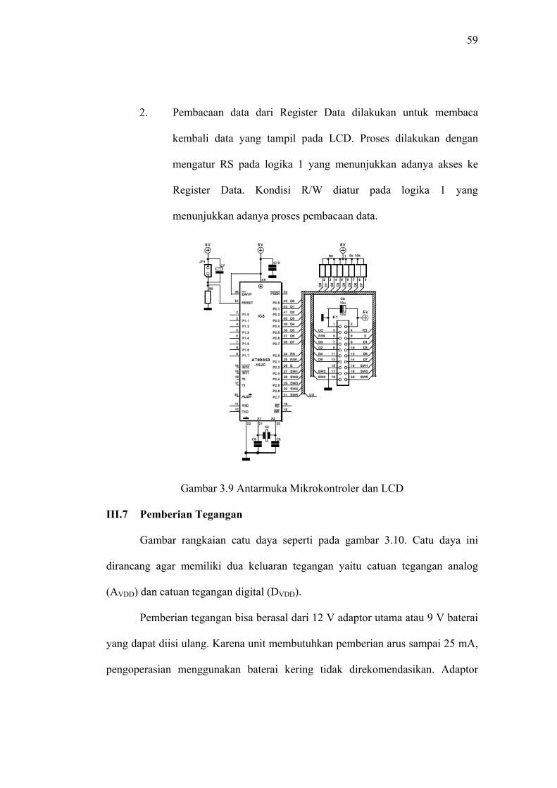
59
2. Pembacaan data dari Register Data dilakukan untuk membaca
kembali data yang tampil pada LCD. Proses dilakukan dengan
mengatur RS pada logika 1 yang menunjukkan adanya akses ke
Register Data. Kondisi R/W diatur pada logika 1 yang
menunjukkan adanya proses pembacaan data.
Gambar 3.9 Antarmuka Mikrokontroler dan LCD
III.7 Pemberian Tegangan
Gambar rangkaian catu daya seperti pada gambar 3.10. Catu daya ini
dirancang agar memiliki dua keluaran tegangan yaitu catuan tegangan analog
(AVDD) dan catuan tegangan digital (DVDD).
Pemberian tegangan bisa berasal dari 12 V adaptor utama atau 9 V baterai
yang dapat diisi ulang. Karena unit membutuhkan pemberian arus sampai 25 mA,
pengoperasian menggunakan baterai kering tidak direkomendasikan. Adaptor
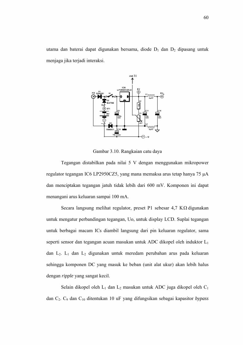
60
utama dan baterai dapat digunakan bersama, diode D1 dan D2 dipasang untuk
menjaga jika terjadi interaksi.
Gambar 3.10. Rangkaian catu daya
Tegangan distabilkan pada nilai 5 V dengan menggunakan mikropower
regulator tegangan IC6 LP2950CZ5, yang mana memaksa arus tetap hanya 75 μA
dan menciptakan tegangan jatuh tidak lebih dari 600 mV. Komponen ini dapat
menangani arus keluaran sampai 100 mA.
Secara langsung melihat regulator, preset P1 sebesar 4,7 K digunakan
untuk mengatur perbandingan tegangan, Uo, untuk display LCD. Suplai tegangan
untuk berbagai macam ICs diambil langsung dari pin keluaran regulator, sama
seperti sensor dan tegangan acuan masukan untuk ADC dikopel oleh induktor L
Ω
1
dan L2. L1 dan L2 digunakan untuk meredam perubahan arus pada keluaran
sehingga komponen DC yang masuk ke beban (unit alat ukur) akan lebih halus
dengan ripple yang sangat kecil.
Selain dikopel oleh L1 dan L2 masukan untuk ADC juga dikopel oleh C1
dan C2. C9 dan C10 ditentukan 10 uF yang difungsikan sebagai kapasitor bypass
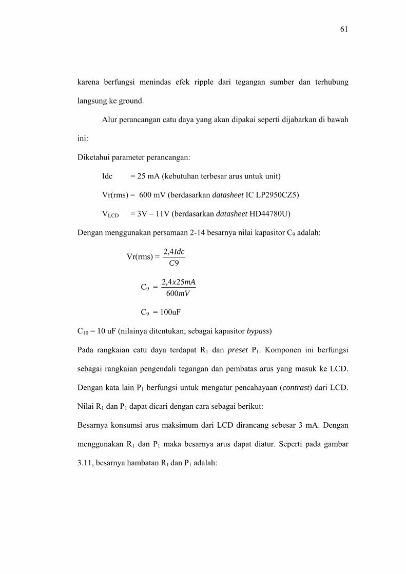
61
karena berfungsi menindas efek ripple dari tegangan sumber dan terhubung
langsung ke ground.
Alur perancangan catu daya yang akan dipakai seperti dijabarkan di bawah
ini:
Diketahui parameter perancangan:
Idc = 25 mA (kebutuhan terbesar arus untuk unit)
Vr(rms) = 600 mV (berdasarkan datasheet IC LP2950CZ5)
VLCD = 3V – 11V (berdasarkan datasheet HD44780U)
Dengan menggunakan persamaan 2-14 besarnya nilai kapasitor C9 adalah:
Vr(rms) = 9
4,2C
Idc
C9 = mV
mAx600
254,2
C9 = 100uF
C10 = 10 uF (nilainya ditentukan; sebagai kapasitor bypass)
Pada rangkaian catu daya terdapat R1 dan preset P1. Komponen ini berfungsi
sebagai rangkaian pengendali tegangan dan pembatas arus yang masuk ke LCD.
Dengan kata lain P1 berfungsi untuk mengatur pencahayaan (contrast) dari LCD.
Nilai R1 dan P1 dapat dicari dengan cara sebagai berikut:
Besarnya konsumsi arus maksimum dari LCD dirancang sebesar 3 mA. Dengan
menggunakan R1 dan P1 maka besarnya arus dapat diatur. Seperti pada gambar
3.11, besarnya hambatan R1 dan P1 adalah:
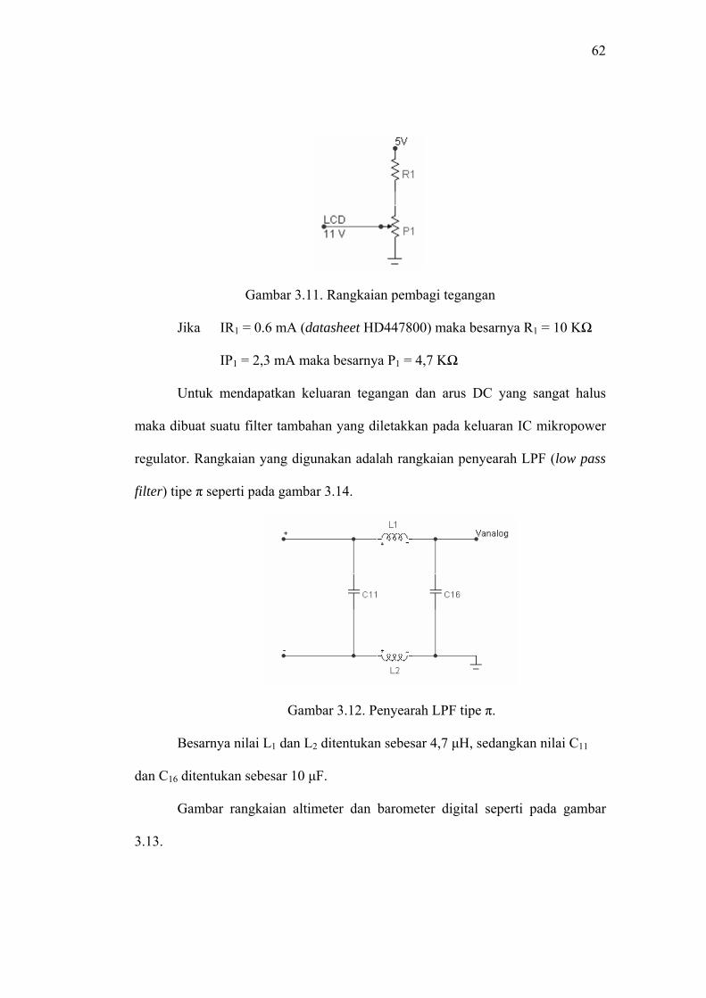
62
Gambar 3.11. Rangkaian pembagi tegangan
Jika IR1 = 0.6 mA (datasheet HD447800) maka besarnya R1 = 10 KΩ
IP1 = 2,3 mA maka besarnya P1 = 4,7 KΩ
Untuk mendapatkan keluaran tegangan dan arus DC yang sangat halus
maka dibuat suatu filter tambahan yang diletakkan pada keluaran IC mikropower
regulator. Rangkaian yang digunakan adalah rangkaian penyearah LPF (low pass
filter) tipe π seperti pada gambar 3.14.
Gambar 3.12. Penyearah LPF tipe π.
Besarnya nilai L1 dan L2 ditentukan sebesar 4,7 μH, sedangkan nilai C11
dan C16 ditentukan sebesar 10 μF.
Gambar rangkaian altimeter dan barometer digital seperti pada gambar
3.13.
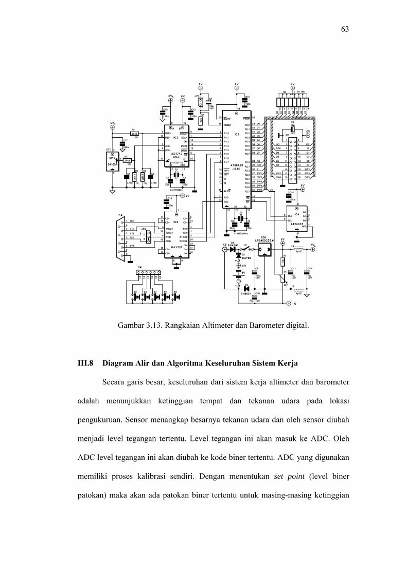
63
Gambar 3.13. Rangkaian Altimeter dan Barometer digital.
III.8 Diagram Alir dan Algoritma Keseluruhan Sistem Kerja
Secara garis besar, keseluruhan dari sistem kerja altimeter dan barometer
adalah menunjukkan ketinggian tempat dan tekanan udara pada lokasi
pengukuruan. Sensor menangkap besarnya tekanan udara dan oleh sensor diubah
menjadi level tegangan tertentu. Level tegangan ini akan masuk ke ADC. Oleh
ADC level tegangan ini akan diubah ke kode biner tertentu. ADC yang digunakan
memiliki proses kalibrasi sendiri. Dengan menentukan set point (level biner
patokan) maka akan ada patokan biner tertentu untuk masing-masing ketinggian
64
tempat dan tekanan udara. ADC dan mikrokontroler dikomunikasikan secara
serial sinkron. Dengan komunikasi serial sinkron maka harus ada proses
sinkronisasi antara mikrokontroler dan ADC, yaitu ADC mengeluarkan clock
sinkronisasi yang menjadi masukan mikrokontroler. LCD dan mikrokontroler
dikomunikasikan melalui bus data, karena itu LCD juga perlu diperiksa. Berikut
adalah algoritma dari sistem kerja altimeter dan barometer digital.
1. Mulai
2. Inisialisasi memori, Port, timer, komunikasi serial dengan ADC, dan LCD
3. Memilih menu untuk altimeter atau barometer
4. Menunggu data dari ADC
5. Membaca data dari ADC
6. Simpan data ke EEPROM
7. Konversi data menjadi data ASCII untuk ditampilkan pada LCD
8. Tampilkan data ketinggian tempat atau tekanan udara pada LCD
9. Kembali ke program awal (mulai)
Dari algoritma diatas, dapat dibuat diagram alir (flow chart) seperti pada
gambar 3.14.
65
Gambar 3.14. Diagram alir sistem kerja altimeter dan barometer
66
III.8.1 Program Utama
Program utama melakukan proses inisialisasi (Port, timer, komunikasi
serial, ADC, dan LCD) dan pembacaan data dari ADC, pemilihan menu, dan
menampilkan data dalam kode ASCII. Proses inisialisasi ADC dan konversi data
biner menjadi kode ASCII menggunakan subrutin tersendiri.
1. Inisialisasi
Pada bagian ini, inisialisasi dilakukan untuk pengesetan awal keseluruhan
Port, memori, timer, komunikasi serial, ADC, dan LCD. Proses inisialisasi
ADC menggunakan subrutin sendiri karena mikrokontroler harus
melakukan proses awal operasi tertentu agar ADC dan mikrokontroler
dapat melakukan komunikasi data serial sinkron.
2. Pemilihan menu altimeter atau barometer
Pemilhan menu ini dilakukan untuk menentukan besaran ketinggian (m)
atau tekanan udara (hPa).
3. Menunggu data dari ADC
Proses ini dilakukan untuk mengecek ada dan tidaknya data pada ADC.
Jika ada data maka dilanjutkan ke proses berikutnya sedangkan jika tidak
ada data maka mikrokontroler akan terus melakukan pengecekan sampai
ada data pada ADC.
4. Membaca data dari ADC
Proses pembacaan data ini akan dilakukan sampai semua data yang ada
pada register data ADC telah diterima mikrokontroler. Jika sudah selesai
maka akan dilanjutkan ke proses berikutnya.
67
5. Simpan data ke EEPROM
Setelah semua data diterima oleh mikrokontroler maka dilakukan proses
penyimpanan ke EEPROM. Data ini adalah data sementara yang nantinya
akan dikonversikan ke kode ASCII.
6. Pengecekan fungsi alat sebagai altimeter atau bukan
Proses ini untuk menentukan data biner ini akan ditampilkan sebagai
besaran ketinggian atau tekanan udara.
7. Konversi data menjadi kode ASCII
Proses ini adalah proses untuk mengubah data menjadi kode ASCII
sehingga dapat ditampilkan pada LCD.
III.9 Diagram alir dan algoritma pengambilan dan pengisian data untuk
ADC
Proses pengambilan dan pengisian data untuk ADC merupakan proses
awal untuk mengendalikan ADC. Proses ini adalah proses pengiriman data dari
mikrokontroler untuk mengeset register komunikasi, membaca register data, dan
menuliskan bit ke register setup, sekaligus juga sebagai proses inisialisasi
kalibrasi. Berikut adalah algoritma untuk mengeset register komunikasi dan
membaca register data.
1. Mulai
2. Mengaktifkan ADC
3. Mencari dan menginisialisasi Port serial mikrokontroler
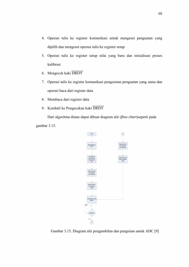
68
4. Operasi tulis ke register komunikasi untuk mengeset penguatan yang
dipilih dan mengeset operasi tulis ke register setup
5. Operasi tulis ke register setup nilai yang baru dan inisialisasi proses
kalibrasi
6. Mengecek kaki DRDY
7. Operasi tulis ke register komunikasi pengesetan penguatan yang sama dan
operasi baca dari register data
8. Membaca dari register data
9. Kembali ke Pengecekan kaki DRDY
Dari algoritma diatas dapat dibuat diagram alir (flow chart)seperti pada
gambar 3.15.
start
Mengaktifkan ADC
Inisialisasi port serial mikrokontr
oler
Operasi tulis ke register komunikasi
Operasi tulis ke register
setup
Mengecek kaki DRDY
Rendah?
C
C
Operasi tulis ke register komunikasi
Operasi baca pada register
data
ya
tidak
Gambar 3.15. Diagram alir pengambilan dan pengisian untuk ADC [9]
69
III.9.1 Program pengambilan dan pengisian data untuk ADC
Proses ini dilakukan untuk mengeset register-register yang ada pada ADC
sehingga komunikasi serial sinkron dapat berjalan dengan baik. Proses ini juga
sebagai kalibrasi data yang akan dikirimkan.
1. Mengaktifkan ADC
ADC diaktifkan dengan cara memberikan tegangan catuan pada kedua
kaki AVDD dan DVDD.
2. Inisialisasi Port serial mikrokontroler
Inisialisasi Port ini dilakukan untuk mengecek Port serial dari
mikrokontroler yang digunakan sebagai jalur komunikasi serial sinkron
antara ADC dan mikrokontroler.
3. Operasi tulis ke register komunikasi ADC
Pada proses ini mikrokontroler mengirimkan data ke ADC untuk mengisi
register komunikasi sehingga register komunikasi dapat mengeset
penguatan yang dipilih dan operasi selanjutnya yang diinginkan untuk
register setup.
4. Operasi tulis ke register setup
Pada proses ini dilakukan pengisian nilai tertentu pada register setup dan
dimulai proses kalibrasi oleh ADC.
5. Mengecek kaki DRDY
Kaki DRDY digunakan sebagai indikator ketika data sudah siap dibaca
oleh mikrokontroler dari register data ADC. DRDY akan aktif rendah
70
ketika data baru telah siap dikirimkan. DRDY akan aktif tinggi lagi ketika
operasi baca dari register data telah selesai.
6. Operasi tulis ke register komunikasi
Pada proses ini akan ditentukan lagi penguatan terpilih yang sama dan
mengeset operasi baca dari register data.
7. Operasi baca dari register data.
Pada proses ini mikrokontroler akan membaca data dari register data ADC.
Proses ini akan terus berlangsung sampai semua data selesai dibaca. Untuk
mengecek proses ini digunakan pengecekan sinyal pada kaki DRDY.
III.10 Diagram Alir dan Algoritma Subroutin Konversi Data
Proses konversi data merupakan proses pengubahan data dari bentuk
hexadesimal (mikrokontroler secara otomatis mengubah data biner menjadi data
hexadesimal) menjadi karakter ASCII sehingga proses pengiriman ke LCD dapat
dilakukan dengan mudah. Hal ini dilakukan karena LCD mampu menerima
karakter ASCII secara langsung. Gambar 3.18 menunjukan diagram alir proses
konversi data menjadi data ASCII.
Algoritma dari proses pengubahan data tersebut adalah :
1. Pengambilan karakter ASCII pada lookup table
2. Pemeriksaan apakah data yang telah diambil sama dengan tabel lookup
yang telah dibuat
3. Tunjuk karakter ASCII yang sesuai dengan tabel lookup
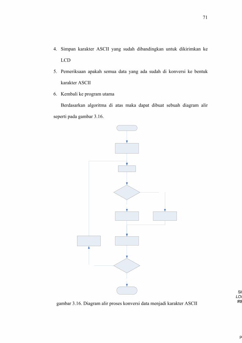
71
4. Simpan karakter ASCII yang sudah dibandingkan untuk dikirimkan ke
LCD
5. Pemeriksaan apakah semua data yang ada sudah di konversi ke bentuk
karakter ASCII
6. Kembali ke program utama
Berdasarkan algoritma di atas maka dapat dibuat sebuah diagram alir
seperti pada gambar 3.16.
gambar 3.16. Diagram alir proses konversi data menjadi karakter ASCII
72
III.10.1 Program Subroutin Konversi Data
Data biner 8 bit yang telah disimpan dalam memori perlu dikonversi
menjadi data ASCII untuk dapat ditampilkan pada LCD secara langsung tanpa
perlu melihat tabel karakter LCD yang dihasilkan dari data hexadesimal.
1. Pengambilan karakter ASCII pada lookup table
Karakter ASCII yang akan digunakan disimpan pada lookup table agar
dengan proses konversi dapat dilakukan dengan lebih mudah. Karakter
yang akan ditampilkan pada LCD berupa angka maka karakter ASCII
yang disimpan pada lookup table adalah 0123456789-+m . * dan hPa.
2. Proses konversi
Pada proses ini, semua data yang sudah disimpan dalam memori diubah
menjadi data ASCII. Proses konversi merupakan satu kesatuan, mulai dari
pemeriksaan karakter hingga semua karakter selesai dibaca dan kembali ke
program utama.
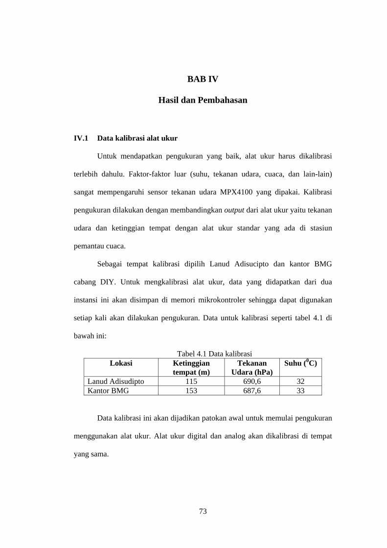
BAB IV
Hasil dan Pembahasan
IV.1 Data kalibrasi alat ukur
Untuk mendapatkan pengukuran yang baik, alat ukur harus dikalibrasi
terlebih dahulu. Faktor-faktor luar (suhu, tekanan udara, cuaca, dan lain-lain)
sangat mempengaruhi sensor tekanan udara MPX4100 yang dipakai. Kalibrasi
pengukuran dilakukan dengan membandingkan output dari alat ukur yaitu tekanan
udara dan ketinggian tempat dengan alat ukur standar yang ada di stasiun
pemantau cuaca.
Sebagai tempat kalibrasi dipilih Lanud Adisucipto dan kantor BMG
cabang DIY. Untuk mengkalibrasi alat ukur, data yang didapatkan dari dua
instansi ini akan disimpan di memori mikrokontroler sehingga dapat digunakan
setiap kali akan dilakukan pengukuran. Data untuk kalibrasi seperti tabel 4.1 di
bawah ini:
Tabel 4.1 Data kalibrasi Lokasi Ketinggian
tempat (m) Tekanan
Udara (hPa) Suhu (0C)
Lanud Adisudipto 115 690,6 32 Kantor BMG 153 687,6 33
Data kalibrasi ini akan dijadikan patokan awal untuk memulai pengukuran
menggunakan alat ukur. Alat ukur digital dan analog akan dikalibrasi di tempat
yang sama.
73
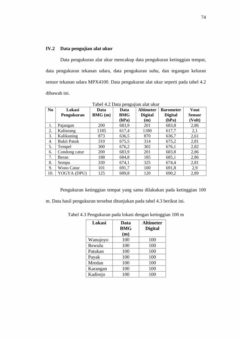
74
IV.2 Data pengujian alat ukur
Data pengukuran alat ukur mencakup data pengukuran ketinggian tempat,
data pengukuran tekanan udara, data pengukuran suhu, dan tegangan keluran
sensor tekanan udara MPX4100. Data pengukuran alat ukur seperti pada tabel 4.2
dibawah ini.
Tabel 4.2 Data pengujian alat ukur No Lokasi
Pengukuran Data
BMG (m)Data BMG (hPa)
Altimeter Digital
(m)
Barometer Digital (hPa)
Vout Sensor (Volt)
1. Pajangan 200 683,9 201 683,8 2,86 2. Kaliurang 1185 617,4 1180 617,7 2,1 3. Kalikuning 873 636,5 870 636,7 2,61 4. Bukit Patuk 310 675,5 314 675,2 2,81 5. Tempel 300 676,2 302 676,1 2,82 6. Condong catur 200 683,9 201 683,8 2,86 7. Beran 188 684,8 185 685,1 2,86 8. Sempu 330 674,1 325 674,4 2,81 9. Wono Catur 101 691,7 100 691,8 2,9
10. YOGYA (DPU) 125 689,8 120 690,2 2,89
Pengukuran ketinggian tempat yang sama dilakukan pada ketinggian 100
m. Data hasil pengukuran tersebut ditunjukan pada tabel 4.3 berikut ini.
Tabel 4.3 Pengukuran pada lokasi dengan ketinggian 100 m
Lokasi Data BMG (m)
Altimeter Digital
Wanujoyo 100 100 Rewulu 100 100 Patukan 100 100 Payak 100 100 Mredan 100 100 Karangan 100 100 Kadirejo 100 100
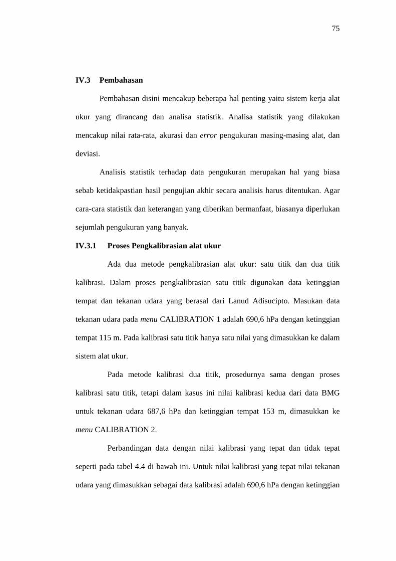
75
IV.3 Pembahasan
Pembahasan disini mencakup beberapa hal penting yaitu sistem kerja alat
ukur yang dirancang dan analisa statistik. Analisa statistik yang dilakukan
mencakup nilai rata-rata, akurasi dan error pengukuran masing-masing alat, dan
deviasi.
Analisis statistik terhadap data pengukuran merupakan hal yang biasa
sebab ketidakpastian hasil pengujian akhir secara analisis harus ditentukan. Agar
cara-cara statistik dan keterangan yang diberikan bermanfaat, biasanya diperlukan
sejumlah pengukuran yang banyak.
IV.3.1 Proses Pengkalibrasian alat ukur
Ada dua metode pengkalibrasian alat ukur: satu titik dan dua titik
kalibrasi. Dalam proses pengkalibrasian satu titik digunakan data ketinggian
tempat dan tekanan udara yang berasal dari Lanud Adisucipto. Masukan data
tekanan udara pada menu CALIBRATION 1 adalah 690,6 hPa dengan ketinggian
tempat 115 m. Pada kalibrasi satu titik hanya satu nilai yang dimasukkan ke dalam
sistem alat ukur.
Pada metode kalibrasi dua titik, prosedurnya sama dengan proses
kalibrasi satu titik, tetapi dalam kasus ini nilai kalibrasi kedua dari data BMG
untuk tekanan udara 687,6 hPa dan ketinggian tempat 153 m, dimasukkan ke
menu CALIBRATION 2.
Perbandingan data dengan nilai kalibrasi yang tepat dan tidak tepat
seperti pada tabel 4.4 di bawah ini. Untuk nilai kalibrasi yang tepat nilai tekanan
udara yang dimasukkan sebagai data kalibrasi adalah 690,6 hPa dengan ketinggian
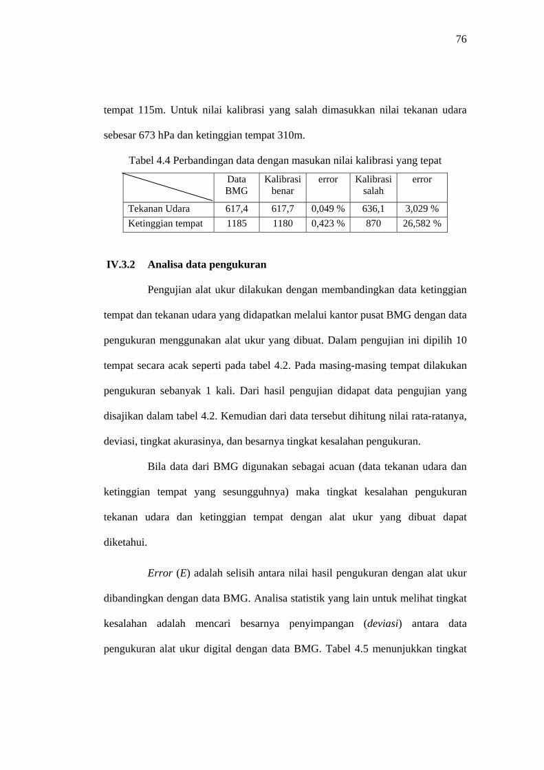
76
tempat 115m. Untuk nilai kalibrasi yang salah dimasukkan nilai tekanan udara
sebesar 673 hPa dan ketinggian tempat 310m.
Tabel 4.4 Perbandingan data dengan masukan nilai kalibrasi yang tepat
Data BMG
Kalibrasi benar
error Kalibrasi salah
error
Tekanan Udara 617,4 617,7 0,049 % 636,1 3,029 % Ketinggian tempat 1185 1180 0,423 % 870 26,582 %
IV.3.2 Analisa data pengukuran
Pengujian alat ukur dilakukan dengan membandingkan data ketinggian
tempat dan tekanan udara yang didapatkan melalui kantor pusat BMG dengan data
pengukuran menggunakan alat ukur yang dibuat. Dalam pengujian ini dipilih 10
tempat secara acak seperti pada tabel 4.2. Pada masing-masing tempat dilakukan
pengukuran sebanyak 1 kali. Dari hasil pengujian didapat data pengujian yang
disajikan dalam tabel 4.2. Kemudian dari data tersebut dihitung nilai rata-ratanya,
deviasi, tingkat akurasinya, dan besarnya tingkat kesalahan pengukuran.
Bila data dari BMG digunakan sebagai acuan (data tekanan udara dan
ketinggian tempat yang sesungguhnya) maka tingkat kesalahan pengukuran
tekanan udara dan ketinggian tempat dengan alat ukur yang dibuat dapat
diketahui.
Error (E) adalah selisih antara nilai hasil pengukuran dengan alat ukur
dibandingkan dengan data BMG. Analisa statistik yang lain untuk melihat tingkat
kesalahan adalah mencari besarnya penyimpangan (deviasi) antara data
pengukuran alat ukur digital dengan data BMG. Tabel 4.5 menunjukkan tingkat
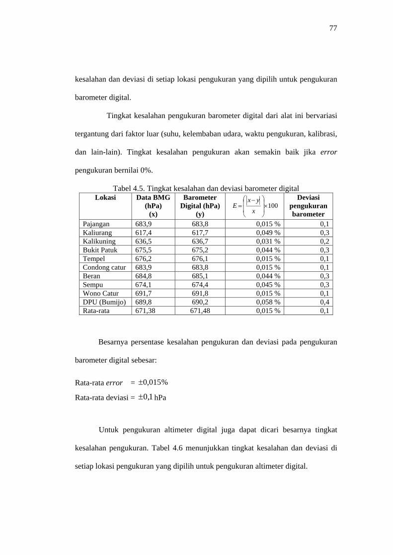
77
kesalahan dan deviasi di setiap lokasi pengukuran yang dipilih untuk pengukuran
barometer digital.
Tingkat kesalahan pengukuran barometer digital dari alat ini bervariasi
tergantung dari faktor luar (suhu, kelembaban udara, waktu pengukuran, kalibrasi,
dan lain-lain). Tingkat kesalahan pengukuran akan semakin baik jika error
pengukuran bernilai 0%.
Tabel 4.5. Tingkat kesalahan dan deviasi barometer digital Lokasi Data BMG
(hPa) (x)
Barometer Digital (hPa)
(y) 100×⎟
⎟
⎠
⎞
⎜⎜
⎝
⎛ −=
xyx
E Deviasi
pengukuran barometer
Pajangan 683,9 683,8 0,015 % 0,1Kaliurang 617,4 617,7 0,049 % 0,3Kalikuning 636,5 636,7 0,031 % 0,2Bukit Patuk 675,5 675,2 0,044 % 0,3Tempel 676,2 676,1 0,015 % 0,1Condong catur 683,9 683,8 0,015 % 0,1Beran 684,8 685,1 0,044 % 0,3Sempu 674,1 674,4 0,045 % 0,3Wono Catur 691,7 691,8 0,015 % 0,1DPU (Bumijo) 689,8 690,2 0,058 % 0,4Rata-rata 671,38 671,48 0,015 % 0,1
Besarnya persentase kesalahan pengukuran dan deviasi pada pengukuran
barometer digital sebesar:
Rata-rata error = %015,0±
Rata-rata deviasi = hPa 1,0±
Untuk pengukuran altimeter digital juga dapat dicari besarnya tingkat
kesalahan pengukuran. Tabel 4.6 menunjukkan tingkat kesalahan dan deviasi di
setiap lokasi pengukuran yang dipilih untuk pengukuran altimeter digital.
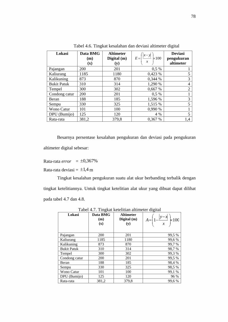
78
Tabel 4.6. Tingkat kesalahan dan deviasi altimeter digital Lokasi Data BMG
(m) (x)
Altimeter Digital (m)
(y) 100×⎟
⎟
⎠
⎞
⎜⎜
⎝
⎛ −=
xyx
E Deviasi
pengukuran altimeter
Pajangan 200 201 0,5 % 1Kaliurang 1185 1180 0,423 % 5Kalikuning 873 870 0,344 % 3Bukit Patuk 310 314 1,290 % 4Tempel 300 302 0,667 % 2Condong catur 200 201 0,5 % 1Beran 188 185 1,596 % 3Sempu 330 325 1,515 % 5Wono Catur 101 100 0,990 % 1DPU (Bumijo) 125 120 4 % 5Rata-rata 381,2 379,8 0,367 % 1,4
Besarnya persentase kesalahan pengukuran dan deviasi pada pengukuran
altimeter digital sebesar:
Rata-rata error = %367,0±
Rata-rata deviasi = m 4,1±
Tingkat kesalahan pengukuran suatu alat ukur berbanding terbalik dengan
tingkat ketelitiannya. Untuk tingkat ketelitian alat ukur yang dibuat dapat dilihat
pada tabel 4.7 dan 4.8.
Tabel 4.7. Tingkat ketelitian altimeter digital Lokasi Data BMG
(m) (x)
Altimeter Digital (m)
(y) 1001 ×⎟
⎟⎠
⎞⎜⎜⎝
⎛ −−=
xxy
A
Pajangan 200 201 99,5 % Kaliurang 1185 1180 99,6 % Kalikuning 873 870 99,7 % Bukit Patuk 310 314 98,7 % Tempel 300 302 99,3 % Condong catur 200 201 99,5 % Beran 188 185 98,4 % Sempu 330 325 98,5 % Wono Catur 101 100 99,1 % DPU (Bumijo) 125 120 96 % Rata-rata 381,2 379,8 99,6 %
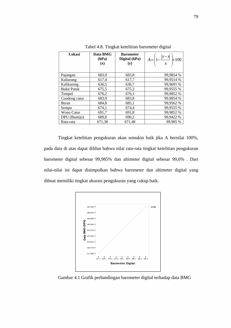
79
Tabel 4.8. Tingkat ketelitian barometer digital Lokasi Data BMG
(hPa) (x)
Barometer Digital (hPa)
(y) 1001 ×⎟
⎟⎠
⎞⎜⎜⎝
⎛ −−=
xxy
A
Pajangan 683,9 683,8 99,9854 % Kaliurang 617,4 617,7 99,9514 % Kalikuning 636,5 636,7 99,9691 % Bukit Patuk 675,5 675,2 99,9555 % Tempel 676,2 676,1 99,9852 % Condong catur 683,9 683,8 99,9854 % Beran 684,8 685,1 99,9562 % Sempu 674,1 674,4 99,9555 % Wono Catur 691,7 691,8 99,9852 % DPU (Bumijo) 689,8 690,2 99,9422 % Rata-rata 671,38 671,48 99,985 %
Tingkat ketelitian pengukuran akan semakin baik jika A bernilai 100%,
pada data di atas dapat dilihat bahwa nilai rata-rata tingkat ketelitian pengukuran
barometer digital sebesar 99,985% dan altimeter digital sebesar 99,6% . Dari
nilai-nilai ini dapat disimpulkan bahwa barometer dan altimeter digital yang
dibuat memiliki tingkat akurasi pengukuran yang cukup baik.
617.7 636.7 674.4 675.2 676.1 683.8 685.1 690.2 691.8
Barometer Digital
617.4900
636.5770
674.0281
675.5260
676.2790
683.9345
684.8690
689.8412
691.7560
Dat
a BM
G (h
Pa)
n=10
Gambar 4.1 Grafik perbandingan barometer digital terhadap data BMG
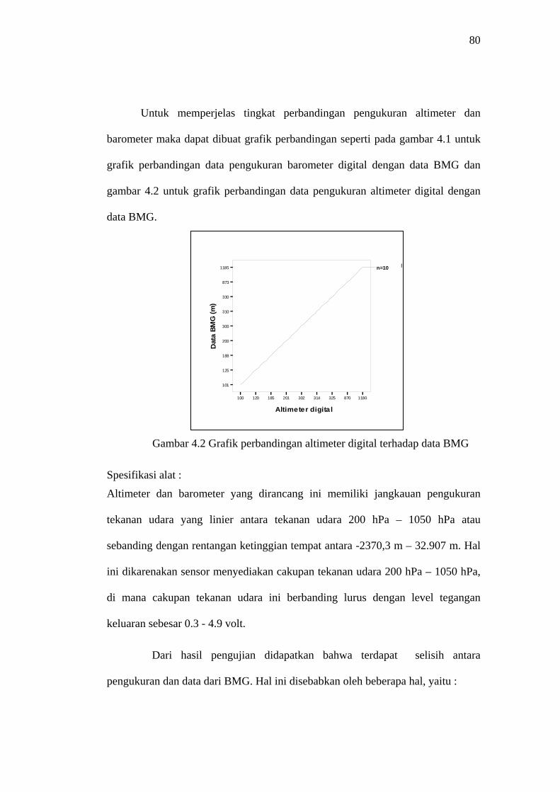
80
Untuk memperjelas tingkat perbandingan pengukuran altimeter dan
barometer maka dapat dibuat grafik perbandingan seperti pada gambar 4.1 untuk
grafik perbandingan data pengukuran barometer digital dengan data BMG dan
gambar 4.2 untuk grafik perbandingan data pengukuran altimeter digital dengan
data BMG.
D
100 120 185 201 302 314 325 870 1180
Altimeter digita l
101
125
188
200
300
310
330
873
1185
Dat
a BM
G (m
)
n=10
Gambar 4.2 Grafik perbandingan altimeter digital terhadap data BMG
Spesifikasi alat :
Altimeter dan barometer yang dirancang ini memiliki jangkauan pengukuran
tekanan udara yang linier antara tekanan udara 200 hPa – 1050 hPa atau
sebanding dengan rentangan ketinggian tempat antara -2370,3 m – 32.907 m. Hal
ini dikarenakan sensor menyediakan cakupan tekanan udara 200 hPa – 1050 hPa,
di mana cakupan tekanan udara ini berbanding lurus dengan level tegangan
keluaran sebesar 0.3 - 4.9 volt.
Dari hasil pengujian didapatkan bahwa terdapat selisih antara
pengukuran dan data dari BMG. Hal ini disebabkan oleh beberapa hal, yaitu :
81
1. Kurang tepatnya nilai kalibrasi untuk alat ukur yang dibuat, atau kalibrasi
berubah selama proses pengukuran.
2. Faktor luar seperti suhu dan kelembaban udara di lingkungan yang berubah
secara ekstrim karena cuaca, ketinggian lokasi, waktu pengukuran, dan lain-
lain.
3. Catu daya yang tidak stabil karena selama alat ukur diaktifkan maka arus yang
digunakan juga cukup banyak sehingga baterai yang digunakan harus diganti
terus menerus.
IV.3.3 Pengoperasian Alat Ukur
Sebelum melakukan pengukuran-pengukuran, biarkan barometer atau
altimeter sekitar 2 menit untuk melakukan ‘pemanasan’. Unit ini dioperasikan
oleh 5 tombol pada panel depan.
1. MODE (S2) tombol untuk mengaktifkan fungsi pada masing-masing menu
untuk diakses dan digunakan.
2. UP ( S3) tombol untuk meningkatkan digit-digit nilai menu yang terpilih.
3. DOWN) ( S4) tombol untuk menurunkan digit-digit nilai menu yang terpilih.
4. ENTER (S5) tombol untuk mengkonfirmasikan untuk menyimpan di eeprom
pilihan pada menu yang dipilih.
5. ESCAPE (S6) tombol untuk mengembalikan ke menu di atasnya tanpa
disimpan di eeprom.
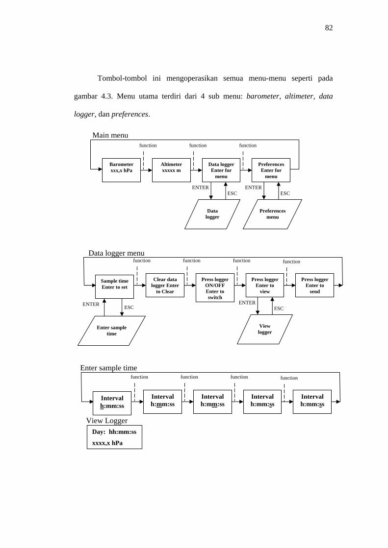
82
Tombol-tombol ini mengoperasikan semua menu-menu seperti pada
gambar 4.3. Menu utama terdiri dari 4 sub menu: barometer, altimeter, data
logger, dan preferences.
ESC ENTER
ESC ENTER
Barometer xxx,x hPa
Altimeter xxxxx m
Data logger Enter for
menu
Preferences Enter for
menu
Data logger
Preferences menu
Main menufunction function function
ESC ENTER
ESC ENTER
Sample time Enter to set
Clear data logger Enter
to Clear
Press logger ON/OFF Enter to switch
Press logger Enter to
view
Enter sample time
View logger
Data logger menu function function function function
Press logger Enter to
send
View Logger
Interval h:mm:ss
Interval h:mm:ss
Interval h:mm:ss
Interval h:mm:ss
Enter sample time function function function function
Interval h:mm:ss
Day: hh:mm:ss
xxxx,x hPa
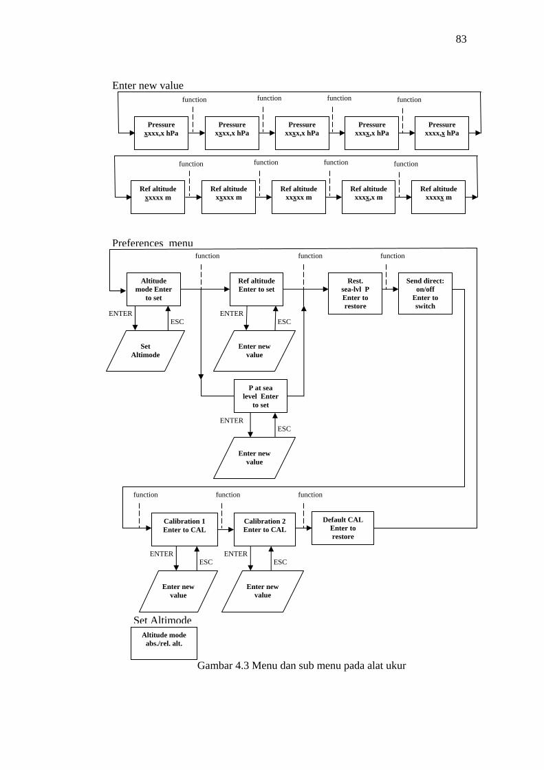
83
Pressure
xxxx,x hPa Pressure
xxxx,x hPa
Pressure xxxx,x hPa
Pressure xxxx,x hPa
Enter new value function function function function
Pressure xxxx,x hPa
Ref altitude xxxxx m
Ref altitude xxxxx m
Ref altitude xxxxx m
Ref altitude xxxx,x m
function function function function
Ref altitude xxxxx m
Gambar 4.3 Menu dan sub menu pada alat ukur
ESC ENTER
ESC ENTER
Altitude mode Enter
to set
Ref altitude Enter to set
Rest. sea-lvl P Enter to restore
Send direct: on/off
Enter to switch
Set Altimode
Enter new value
Preferences menufunction function function
P at sea level Enter
to set
Enter new value
ENTER ESC
ESC ENTER
ESC ENTER
Default CAL Enter to restore
Calibration 1 Enter to CAL
Calibration 2 Enter to CAL
Enter new value
Enter new value
function function function
Altitude mode abs./rel. alt.
Set Altimode
84
Sub menu penyimpan data itu sendiri terdiri dari beberapa sub-sub
menu lagi seperti ditunjukkan pada gambar 4.3. Ketika masukan sample time
dipilih, interval sampling harus diatur antara 10 detik dan 8 jam dengan resolusi
satu detik. Hsil pengukuran disimpan di penyimpan data dan dapat dilihat dengan
memilih menu view logger.
Rincian menu preferences berisi fungsi ‘Ref Altitude’ untuk program
normal.hex dan ‘P at Sea Level’ untuk program vsl.hex. Untuk kedua jenis
program, selama proses kalibrasi, masukan nilai ketinggian atau tekanan udara ke
‘Input New Value’ digit demi digit. ‘Set Altimode’ untuk memilih ketinggian
absolut atau ketinggian relatif untuk ditampilkan. Ketingian absolut adalah
ketingian di atas permukaan laut, dan ketingian relatif adalah ketingian di atas
sebuah ketinggian referensi. Pada kedua program, nilai tekanan udara di atas
permukaan laut yang aktual harus dimasukkan. Referensi tekanan udara di atas
permukaan laut adalah 1013,25 millibar(1013,25 hPa), di-reset dengan pilihan
‘Rest. sea-|v|P’. ‘Default cal’ menghasilkan fungsi yang sama: ini menghapus
semua masukan-masukan kalibrasi dan menggantikannya dengan nilai standar.
Dua tanda panah menunjukkan nilai pengukuran sedang naik atau turun. Ketika
data logger aktif, pada display ada tanda bintang.
IV.3.4 Analisa sistem kerja
Untuk menganalisa sistem kerja alat ukur yang dibuat dapat dilihat dari
kinerja dari masing-masing komponen yang dipakai mulai dari sensor, ADC,
mikrokontroler, dan LCD.
85
IV.3.4.1 Sensor MPX4100
Bagian terpenting dari sensor tekanan udara MPX4100 adalah
kemampuan mengubah variasi tekanan udara lingkungan menjadi
besaran listrik.
Variabel dari sensor yang harus dianalisa adalah Vout sensor.
Untuk mengukur besarnya Vout sensor digunakan multimeter digital.
Vout sensor ini nantinya akan mempengaruhi perubahan data digital
pada register data ADC. Hasil pengukuran Vout sensor pada beberapa
lokasi pengukuran seperti pada tabel 4.9. Nilai Vout sensor hasil
perhitungan disesuaikan dengan persamaan 3.1.
Tabel 4.9. Perbandingan Vout sensor Lokasi
Pengukuran Data BMG (hPa)
Vout Sensor perhitungan
(Volt)
Vout Sensor pengukuran
(Volt) 100×⎟
⎟
⎠
⎞
⎜⎜
⎝
⎛ −=
xyx
E
Pajangan 683,8 2,8624 2,86 1,481 % Kaliurang 617,7 2,106 2,1 0,189 % Kalikuning 636,7 2,6127 2,61 0,486 % Bukit Patuk 675,2 2,8163 2,81 0,487 % Tempel 676,1 2,8211 2,82 0,039 % Condong catur 683,8 2,8624 2,86 1,481 % Beran 685,1 2,8686 2,86 1,095 % Sempu 674,4 2,8120 2,81 0,285 % Wono Catur 691,8 2,9043 2,9 0,196 % YOGYA (DPU) 690,2 2,8958 2,89 0,145 % Jumlah total 6714,8 27,5616 2,86 5,884 % Rata-rata 671,48 2,75616 2,1 0,115 %
Berdasarkan persaman 3.1 maka semakin besar tekanan udara
maka Vout sensor akan semakin besar pula. Jika data hasil pengukuran
Vout sensor menggunakan multimeter digital dibandingkan dengan data
hasil perhitungan didapatkan tingkat kesalahan rata-rata sebesar 0,115
%. Hal ini menandakan bahwa alat ukur telah bekerja cukup baik karena
86
tingkat kesalahan mendekati 0 %. Untuk data pengukuran vout sensor
jika dibandingkan dengan tekanan udara terukur seperti pada gambar
4.4.
617,7; 2,1
636,7; 2,61
691,8; 2,9
22,052,1
2,152,2
2,252,3
2,352,4
2,452,5
2,552,6
2,652,7
2,752,8
2,852,9
2,953
600 620 640 660 680 700Tekanan Udara (hPa)
Vout
Sen
sor (
volt)
Gambar 4.4 Perbandingan Vout sensor terhadap Data tekanan udara
BMG
IV.3.4.2 Analog to Digital Converter AD7715
Bagian terpenting dari komponen AD7715 adalah kemampuan
mengubah besaran analog menjadi besaran digital. Komunikasi data
yang digunakan antara mikrokontroler dan AD7715 adalah komunikasi
data serial sinkron dengan frame bit oriented. Data pengamatan untuk
komunikasi data antara mikrokontroler dan ADC menggunakan dua
buah LED pada jalur Dout dan Din.
Pada saat pengamatan diketahui bahwa komunikasi data antara
mikrokontroler dan ADC berjalan dengan baik karena kedua LED
menyala secara bergantian pada saat terjadi komunikasi data.
87
Pengamatan untuk komunikasi data juga dilakukan menggunakan
osiloskop digital
Besarnya baud rate dari ADC dapat ditentukan dari fCLK IN.
Dengan merancang penguatan ADC maksimum sebesar 128, laju
sampling masukan (baud rate) untuk AD7715 berada pada fCLK IN/128
(19.2 kHz pada fCLK IN = 2.4576 MHz). Dengan menggunakan kristal
2.4576 MHz maka fCLK IN dapat dipastikan bekerja pada rentangan 400
KHz sampai 2.5 MHz. Dengan adanya rentangan ini maka nilai baud
rate juga bervariasi tergantung besarnya penguatan yang dipakai.
Pada saat pengukuran menggunakan osiloskop digital dan
frekuensi counter didapatkan data sebagai berikut:
1. Besarnya frekuensi pada pin 1 (SCLK) AD7715 adalah minimum
17,65 KHz dan maksimum 903 KHz. Gambar gelombangnya
seperti pada gambar 4.5.
Gambar 4.5 Gelombang keluaran pin 1 (SCLK)
2. Besarnya frekuensi pada pin 14 (DIN) adalah 10,7 MHz. Ini adalah
besarnya laju data saat mikrokontroler melaksanakan siklus write.
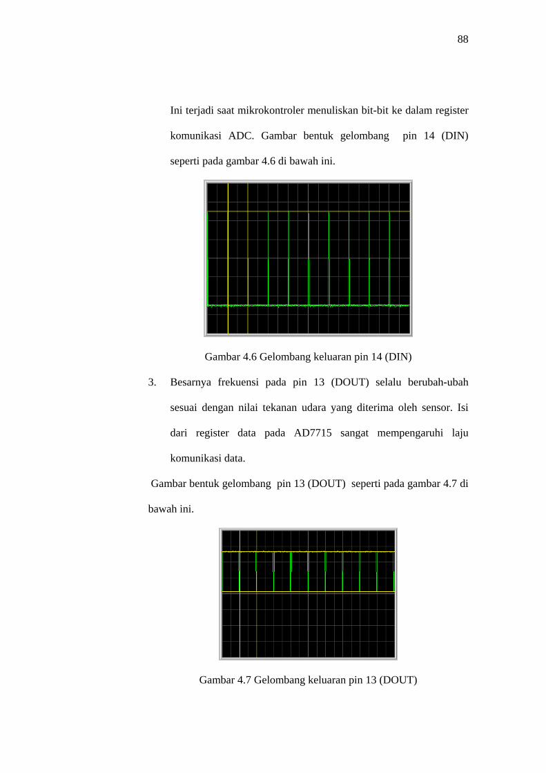
88
Ini terjadi saat mikrokontroler menuliskan bit-bit ke dalam register
komunikasi ADC. Gambar bentuk gelombang pin 14 (DIN)
seperti pada gambar 4.6 di bawah ini.
Gambar 4.6 Gelombang keluaran pin 14 (DIN)
3. Besarnya frekuensi pada pin 13 (DOUT) selalu berubah-ubah
sesuai dengan nilai tekanan udara yang diterima oleh sensor. Isi
dari register data pada AD7715 sangat mempengaruhi laju
komunikasi data.
Gambar bentuk gelombang pin 13 (DOUT) seperti pada gambar 4.7 di
bawah ini.
Gambar 4.7 Gelombang keluaran pin 13 (DOUT)
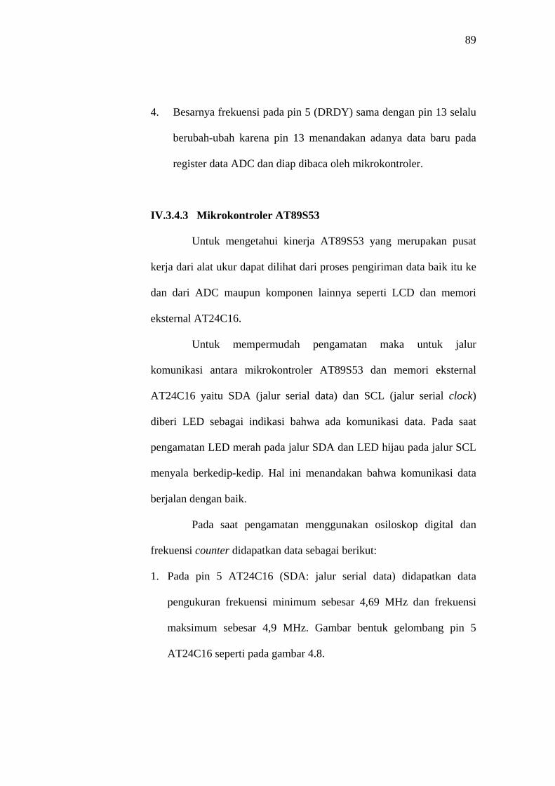
89
4. Besarnya frekuensi pada pin 5 (DRDY) sama dengan pin 13 selalu
berubah-ubah karena pin 13 menandakan adanya data baru pada
register data ADC dan diap dibaca oleh mikrokontroler.
IV.3.4.3 Mikrokontroler AT89S53
Untuk mengetahui kinerja AT89S53 yang merupakan pusat
kerja dari alat ukur dapat dilihat dari proses pengiriman data baik itu ke
dan dari ADC maupun komponen lainnya seperti LCD dan memori
eksternal AT24C16.
Untuk mempermudah pengamatan maka untuk jalur
komunikasi antara mikrokontroler AT89S53 dan memori eksternal
AT24C16 yaitu SDA (jalur serial data) dan SCL (jalur serial clock)
diberi LED sebagai indikasi bahwa ada komunikasi data. Pada saat
pengamatan LED merah pada jalur SDA dan LED hijau pada jalur SCL
menyala berkedip-kedip. Hal ini menandakan bahwa komunikasi data
berjalan dengan baik.
Pada saat pengamatan menggunakan osiloskop digital dan
frekuensi counter didapatkan data sebagai berikut:
1. Pada pin 5 AT24C16 (SDA: jalur serial data) didapatkan data
pengukuran frekuensi minimum sebesar 4,69 MHz dan frekuensi
maksimum sebesar 4,9 MHz. Gambar bentuk gelombang pin 5
AT24C16 seperti pada gambar 4.8.
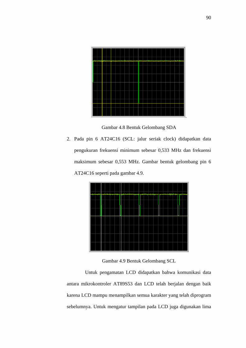
90
.
Gambar 4.8 Bentuk Gelombang SDA
2. Pada pin 6 AT24C16 (SCL: jalur seriak clock) didapatkan data
pengukuran frekuensi minimum sebesar 0,533 MHz dan frekuensi
maksimum sebesar 0,553 MHz. Gambar bentuk gelombang pin 6
AT24C16 seperti pada gambar 4.9.
Gambar 4.9 Bentuk Gelombang SCL
Untuk pengamatan LCD didapatkan bahwa komunikasi data
antara mikrokontroler AT89S53 dan LCD telah berjalan dengan baik
karena LCD mampu menampilkan semua karakter yang telah diprogram
sebelumnya. Untuk mengatur tampilan pada LCD juga digunakan lima

91
switch yang juga telah diatur oleh program pada mikrokontroler. Karena
mikrokontroler adalah pusat kontrol alat ukur maka semua komponen
yang terkoneksi akan diatur oleh program yang telah dimasukan
sebelumnya.
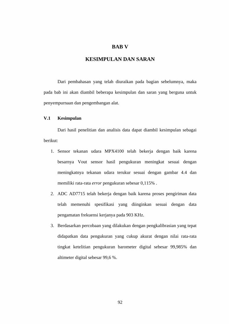
BAB V
KESIMPULAN DAN SARAN
Dari pembahasan yang telah diuraikan pada bagian sebelumnya, maka
pada bab ini akan diambil beberapa kesimpulan dan saran yang berguna untuk
penyempurnaan dan pengembangan alat.
V.1 Kesimpulan
Dari hasil penelitian dan analisis data dapat diambil kesimpulan sebagai
berikut:
1. Sensor tekanan udara MPX4100 telah bekerja dengan baik karena
besarnya Vout sensor hasil pengukuran meningkat sesuai dengan
meningkatnya tekanan udara terukur sesuai dengan gambar 4.4 dan
memiliki rata-rata error pengukuran sebesar 0,115% .
2. ADC AD7715 telah bekerja dengan baik karena proses pengiriman data
telah memenuhi spesifikasi yang diinginkan sesuai dengan data
pengamatan frekuensi kerjanya pada 903 KHz.
3. Berdasarkan percobaan yang dilakukan dengan pengkalibrasian yang tepat
didapatkan data pengukuran yang cukup akurat dengan nilai rata-rata
tingkat ketelitian pengukuran barometer digital sebesar 99,985% dan
altimeter digital sebesar 99,6 %.
92
93
4. Jika alat ukur tidak terkalibrasi secara benar maka tingkat kesalahan sangat
besar. Besarnya tingkat kesalahan tanpa nilai kalibrasi yang tepat untuk
satu titik pengukuran adalah:
a. Data kalibrasi benar:
error tekanan udara sebesar 0,049 % dan ketinggian tempat 0,423 %.
b. Data kalibrasi salah :
error tekanan udara sebesar 3,029 % dan ketinggian tempat 26,582 %.
5. Pada pengukuran tekanan udara dan ketinggian tempat masih terdapat
kesalahan data pengukuran terhadap data BMG dengan besarnya
persentase kesalahan pengukuran dan deviasi serta rata-rata tingkat
ketelitian pada pengukuran barometer digital dan altimeter digital sebesar:
a. Barometer digital
Rata-rata error = %015,0±
Rata-rata deviasi = 1,0± hPa
Rata-rata tingkat ketelitian = 99,985%
b. Altimeter digital
Rata-rata error = %367,0±
Rata-rata deviasi = 4,1± m
Rata-rata tingkat ketelitian = 99,6%
94
V.2 Saran
Untuk pengembangan alat selanjutnya dapat diajukan beberapa saran
sebagai berikut.
1. Untuk pengukuran di atas 3000 mdpl dapat ditambahkan sistem transmisi
jarak jauh (telemetri) menggunakan teknik komunikasi tertentu dan dibuat
dengan berbasis PC sehingga hasil pengukuran ketinggian tempat dan tekanan
udara dapat terus menerus terpantau.
2. Untuk penggunaan di lapangan dapat ditambahkan termometer digital sehinga
dapat menjadi alat yang multifungsi.
3. Melakukan pengecekan secara berkala (disarankan setiap 15 menit) untuk nilai
kalibrasi selama proses pengukuran dilakukan karena alat ukur yang dirancang
seringkali mengabaikan faktor luar misalnya goncangan, waktu pengukuran,
cuaca, dan lain-lain.
4. Dapat ditambahkan sebuah rangkaian penguat tertentu sebagai alat untuk
mendeteksi hujan.
xx
DAFTAR PUSTAKA
[1] Beckwith Thomas G., Buck N. Lewis, Marangoni Roy D., Pengukuran
Mekanis, Erlangga, 1987, Jakarta.
[2] Boylestad, Robert., Nashelsky, Louis., Electronic Devices & Circuit
Theory 6th edition, Prentice Hall, Englewood Cliff, A Simon & Schuster
Company, New Jersey.
[3] Cooper, W.D., Instrumentasi Elektronika & Teknik Pengukuran, edisi II,
Erlangga, Jakarta.
[4] Eko Putra, Agfianto, Belajar Mikrokontroler AT89C51/52/55 (Teori dan
Aplikasi, Gava Media, Yogyakarta, 2004.
[5] Luethi, Peter., Precision Digital Altimeter using MPX4100
[6] Mornhinweg, Manfred., Alti-variometer, 1998
[7] Stallings, Wiliam., Komunikasi data dan komputer: Dasar-dasar
komunikasi data, Salemba Teknika.
[8] Vaclavik, Radek., Digital Altimeter
[9] _______________., 16-Bit, Sigma Delta ADC AD7715 Datasheet,
Analog Devices, Inc., 2000.
http://www.analog.com
[10] _______________., 8-Bit Microcontroller with 12K Bytes Flash
AT89S53 Datasheet, Atmel Corporation., 2000.
http://www.Atmel.com
xxi
[11] _____________., Integrated Silicon Pressure Sensor for Manifold
Absolute Pressure Applications On-Chip Signal Conditioned,
Temperatured Compesated and Calibrated MPX4100 Datasheet,
Motorola, inc., 2001.
http://www.Motorola.com
[12] _____________., Dot Matrix Liquid Crystal Display Controller/Driver
HD44780U datasheet, Hitachi, inc., 2000.
http://pdf.alldatasheet.net
[13] _______________., Altimeter, Wikipedia, the free encyclopedia. Media
Wiki. September 2006.
http://en.wikipedia.org/wiki/Altimeter
[14] _______________., Barometer, Wikipedia, the free encyclopedia. Media
Wiki. September 2006.
http://en.wikipedia.org/wiki/Barometer
[15] Suparman, I.A., Metode Analisis Tabel Silang –1 Menggunakan analisis
nilai mutlak dan Persentase, 2000.
http://www.statistik-suparman.net
[16] Trochim, W.M.A., Measurement Error, 2006.
http://www.statsoft.com/textbook/stathome.html

Lampiran
1
Features• Compatible with MCS-51™ Products• 12K Bytes of In-System Reprogrammable Downloadable Flash Memory
– SPI Serial Interface for Program Downloading– Endurance: 1,000 Write/Erase Cycles
• 4V to 6V Operating Range• Fully Static Operation: 0 Hz to 24 MHz• Three-level Program Memory Lock• 256 x 8-bit Internal RAM• 32 Programmable I/O Lines• Three 16-bit Timer/Counters• Nine Interrupt Sources• Programmable UART Serial Channel• SPI Serial Interface• Low-power Idle and Power-down Modes• Interrupt Recovery From Power-down• Programmable Watchdog Timer• Dual Data Pointer• Power-off Flag
DescriptionThe AT89S53 is a low-power, high-performance CMOS 8-bit microcomputer with 12Kbytes of downloadable Flash programmable and erasable read only memory. Thedevice is manufactured using Atmel’s high-density nonvolatile memory technologyand is compatible with the industry-standard 80C51 instruction set and pinout. The on-chip downloadable Flash allows the program memory to be reprogrammed in-systemthrough an SPI serial interface or by a conventional nonvolatile memory programmer.By combining a versatile 8-bit CPU with downloadable Flash on a monolithic chip, theAtmel AT89S53 is a powerful microcomputer which provides a highly-flexible andcost-effective solution to many embedded control applications.
The AT89S53 provides the following standard features: 12K bytes of downloadableFlash, 256 bytes of RAM, 32 I/O lines, programmable watchdog timer, two Data Point-ers, three 16-bit timer/counters, a six-vector two-level interrupt architecture, a fullduplex serial port, on-chip oscillator, and clock circuitry. In addition, the AT89S53 isdesigned with static logic for operation down to zero frequency and supports two soft-ware selectable power saving modes. The Idle Mode stops the CPU while allowing theRAM, timer/counters, serial port, and interrupt system to continue functioning. ThePower-down mode saves the RAM contents but freezes the oscillator, disabling allother chip functions until the next interrupt or hardware reset.
The downloadable Flash can change a single byte at a time and is accessible throughthe SPI serial interface. Holding RESET active forces the SPI bus into a serial pro-gramming interface and allows the program memory to be written to or read fromunless Lock Bit 2 has been activated.
Rev. 0787D–06/00
8-bit Microcontroller with 12K Bytes Flash
AT89S53
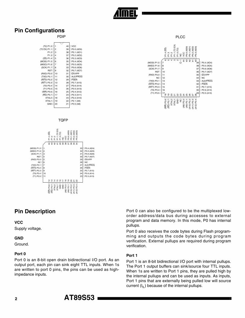
AT89S532
Pin Description
VCC
Supply voltage.
GND
Ground.
Port 0
Port 0 is an 8-bit open drain bidirectional I/O port. As anoutput port, each pin can sink eight TTL inputs. When 1sare written to port 0 pins, the pins can be used as high-impedance inputs.
Port 0 can also be configured to be the multiplexed low-order address/data bus during accesses to externalprogram and data memory. In this mode, P0 has internalpullups.
Port 0 also receives the code bytes during Flash program-ming and outputs the code bytes dur ing programverification. External pullups are required during programverification.
Port 1
Port 1 is an 8-bit bidirectional I/O port with internal pullups.The Port 1 output buffers can sink/source four TTL inputs.When 1s are written to Port 1 pins, they are pulled high bythe internal pullups and can be used as inputs. As inputs,Port 1 pins that are externally being pulled low will sourcecurrent (IIL) because of the internal pullups.
Pin ConfigurationsPDIP
1234567891011121314151617181920
4039383736353433323130292827262524232221
(T2) P1.0(T2 EX) P1.1
P1.2P1.3
(SS) P1.4(MOSI) P1.5(MISO) P1.6(SCK) P1.7
RST(RXD) P3.0(TXD) P3.1(INT0) P3.2(INT1) P3.3
(T0) P3.4(T1) P3.5
(WR) P3.6(RD) P3.7
XTAL2XTAL1
GND
VCCP0.0 (AD0)P0.1 (AD1)P0.2 (AD2)P0.3 (AD3)P0.4 (AD4)P0.5 (AD5)P0.6 (AD6)P0.7 (AD7)EA/VPPALE/PROGPSENP2.7 (A15)P2.6 (A14)P2.5 (A13)P2.4 (A12)P2.3 (A11)P2.2 (A10)P2.1 (A9)P2.0 (A8)
PLCC
7891011121314151617
3938373635343332313029
(MOSI) P1.5(MISO) P1.6(SCK) P1.7
RST(RXD) P3.0
NC(TXD) P3.1(INT0) P3.2(INT1) P3.3
(T0) P3.4(T1) P3.5
P0.4 (AD4)P0.5 (AD5)P0.6 (AD6)P0.7 (AD7)EA/VPPNCALE/PROGPSENP2.7 (A15)P2.6 (A14)P2.5 (A13)
6 5 4 3 2 1 44 43 42 41 40
18 19 20 21 22 23 24 25 26 27 28
(WR
) P
3.6
(RD
) P
3.7
XT
AL2
XT
AL1
GN
DN
C(A
8) P
2.0
(A9)
P2.
1(A
10)
P2.
2(A
11)
P2.
3(A
12)
P2.
4
P1.
4 (S
S)
P1.
3P
1.2
P1.
1 (T
2 E
X)
P1.
0 (T
2)N
CV
CC
P0.
0 (A
D0)
P0.
1 (A
D1)
P0.
2 (A
D2)
P0.
3 (A
D3)
TQFP
1234567891011
3332313029282726252423
44 43 42 41 40 39 38 37 36 35 34
12 13 14 15 16 17 18 19 20 21 22
(MOSI) P1.5(MISO) P1.6(SCK) P1.7
RST(RXD) P3.0
NC(TXD) P3.1(INT0) P3.2(INT1) P3.3
(T0) P3.4(T1) P3.5
P0.4 (AD4)P0.5 (AD5)P0.6 (AD6)P0.7 (AD7)EA/VPPNCALE/PROGPSENP2.7 (A15)P2.6 (A14)P2.5 (A13)
P1.
4 (S
S)
P1.
3P
1.2
P1.
1 (T
2 E
X)
P1.
0 (T
2)N
CV
CC
P0.
0 (A
D0)
P0.
1 (A
D1)
P0.
2 (A
D2)
P0.
3 (A
D3)
(WR
) P
3.6
(RD
) P
3.7
XT
AL2
XT
AL1
GN
DG
ND
(A8)
P2.
0(A
9) P
2.1
(A10
) P
2.2
(A11
) P
2.3
(A12
) P
2.4
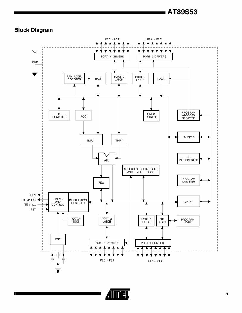
AT89S53
3
Block Diagram
PORT 2 DRIVERS
PORT 2LATCH
P2.0 - P2.7
FLASHPORT 0LATCHRAM
PROGRAMADDRESSREGISTER
BUFFER
PCINCREMENTER
PROGRAMCOUNTER
DPTRINSTRUCTIONREGISTER
BREGISTER
INTERRUPT, SERIAL PORT,AND TIMER BLOCKS
STACKPOINTERACC
TMP2 TMP1
ALU
PSW
TIMINGAND
CONTROL
PORT 1 DRIVERS
P1.0 - P1.7
PORT 3LATCH
PORT 3 DRIVERS
P3.0 - P3.7
OSC
GND
VCC
PSEN
ALE/PROG
EA / VPP
RST
RAM ADDR.REGISTER
PORT 0 DRIVERS
P0.0 - P0.7
PORT 1LATCH
WATCHDOG
SPIPORT
PROGRAMLOGIC
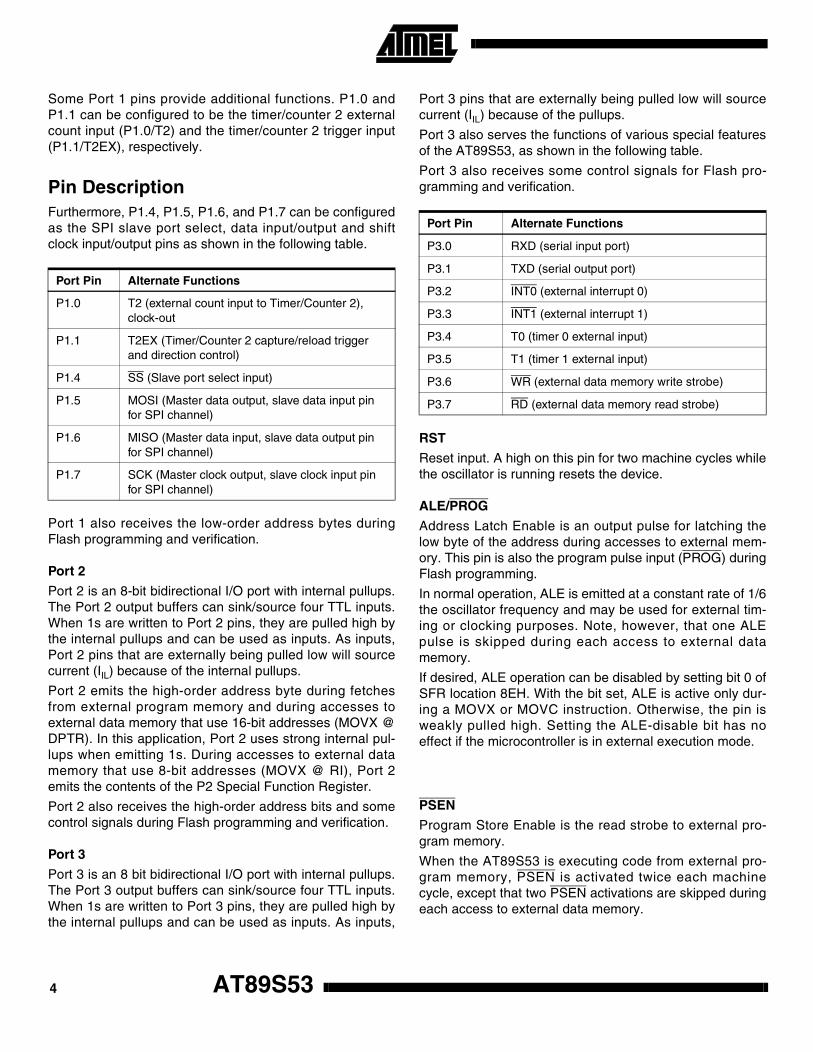
AT89S534
Some Port 1 pins provide additional functions. P1.0 andP1.1 can be configured to be the timer/counter 2 externalcount input (P1.0/T2) and the timer/counter 2 trigger input(P1.1/T2EX), respectively.
Pin DescriptionFurthermore, P1.4, P1.5, P1.6, and P1.7 can be configuredas the SPI slave port select, data input/output and shiftclock input/output pins as shown in the following table.
Port 1 also receives the low-order address bytes duringFlash programming and verification.
Port 2
Port 2 is an 8-bit bidirectional I/O port with internal pullups.The Port 2 output buffers can sink/source four TTL inputs.When 1s are written to Port 2 pins, they are pulled high bythe internal pullups and can be used as inputs. As inputs,Port 2 pins that are externally being pulled low will sourcecurrent (IIL) because of the internal pullups.
Port 2 emits the high-order address byte during fetchesfrom external program memory and during accesses toexternal data memory that use 16-bit addresses (MOVX @DPTR). In this application, Port 2 uses strong internal pul-lups when emitting 1s. During accesses to external datamemory that use 8-bit addresses (MOVX @ RI), Port 2emits the contents of the P2 Special Function Register.
Port 2 also receives the high-order address bits and somecontrol signals during Flash programming and verification.
Port 3
Port 3 is an 8 bit bidirectional I/O port with internal pullups.The Port 3 output buffers can sink/source four TTL inputs.When 1s are written to Port 3 pins, they are pulled high bythe internal pullups and can be used as inputs. As inputs,
Port 3 pins that are externally being pulled low will sourcecurrent (IIL) because of the pullups.
Port 3 also serves the functions of various special featuresof the AT89S53, as shown in the following table.
Port 3 also receives some control signals for Flash pro-gramming and verification.
RST
Reset input. A high on this pin for two machine cycles whilethe oscillator is running resets the device.
ALE/PROG
Address Latch Enable is an output pulse for latching thelow byte of the address during accesses to external mem-ory. This pin is also the program pulse input (PROG) duringFlash programming.
In normal operation, ALE is emitted at a constant rate of 1/6the oscillator frequency and may be used for external tim-ing or clocking purposes. Note, however, that one ALEpulse is skipped during each access to external datamemory.
If desired, ALE operation can be disabled by setting bit 0 ofSFR location 8EH. With the bit set, ALE is active only dur-ing a MOVX or MOVC instruction. Otherwise, the pin isweakly pulled high. Setting the ALE-disable bit has noeffect if the microcontroller is in external execution mode.
PSEN
Program Store Enable is the read strobe to external pro-gram memory.
When the AT89S53 is executing code from external pro-gram memory, PSEN is activated twice each machinecycle, except that two PSEN activations are skipped duringeach access to external data memory.
Port Pin Alternate Functions
P1.0 T2 (external count input to Timer/Counter 2), clock-out
P1.1 T2EX (Timer/Counter 2 capture/reload trigger and direction control)
P1.4 SS (Slave port select input)
P1.5 MOSI (Master data output, slave data input pin for SPI channel)
P1.6 MISO (Master data input, slave data output pin for SPI channel)
P1.7 SCK (Master clock output, slave clock input pin for SPI channel)
Port Pin Alternate Functions
P3.0 RXD (serial input port)
P3.1 TXD (serial output port)
P3.2 INT0 (external interrupt 0)
P3.3 INT1 (external interrupt 1)
P3.4 T0 (timer 0 external input)
P3.5 T1 (timer 1 external input)
P3.6 WR (external data memory write strobe)
P3.7 RD (external data memory read strobe)
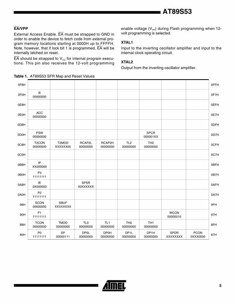
AT89S53
5
EA/VPP
External Access Enable. EA must be strapped to GND inorder to enable the device to fetch code from external pro-gram memory locations starting at 0000H up to FFFFH.Note, however, that if lock bit 1 is programmed, EA will beinternally latched on reset.
EA should be strapped to VCC for internal program execu-tions. This pin also receives the 12-volt programming
enable voltage (VPP) during Flash programming when 12-volt programming is selected.
XTAL1
Input to the inverting oscillator amplifier and input to theinternal clock operating circuit.
XTAL2
Output from the inverting oscillator amplifier.
Table 1. AT89S53 SFR Map and Reset Values
0F8H 0FFH
0F0HB
000000000F7H
0E8H 0EFH
0E0HACC
000000000E7H
0D8H 0DFH
0D0HPSW
00000000SPCR
000001XX0D7H
0C8HT2CON
00000000T2MOD
XXXXXX00RCAP2L00000000
RCAP2H00000000
TL200000000
TH200000000
0CFH
0C0H 0C7H
0B8HIP
XX0000000BFH
0B0HP3
111111110B7H
0A8HIE
0X000000SPSR
00XXXXXX0AFH
0A0HP2
111111110A7H
98HSCON
00000000SBUF
XXXXXXXX9FH
90HP1
11111111WCON
0000001097H
88HTCON
00000000TMOD
00000000TL0
00000000TL1
00000000TH0
00000000TH1
000000008FH
80HP0
11111111SP
00000111DP0L
00000000DP0H
00000000DP1L
00000000DP1H
00000000SPDR
XXXXXXXXPCON
0XXX000087H
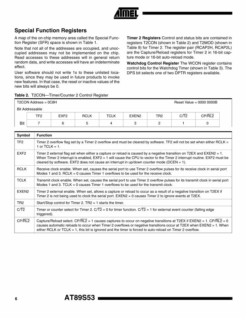
AT89S536
Special Function RegistersA map of the on-chip memory area called the Special Func-tion Register (SFR) space is shown in Table 1.
Note that not all of the addresses are occupied, and unoc-cupied addresses may not be implemented on the chip.Read accesses to these addresses will in general returnrandom data, and write accesses will have an indeterminateeffect.
User software should not write 1s to these unlisted loca-tions, since they may be used in future products to invokenew features. In that case, the reset or inactive values of thenew bits will always be 0.
Timer 2 Registers Control and status bits are contained inregisters T2CON (shown in Table 2) and T2MOD (shown inTable 9) for Timer 2. The register pair (RCAP2H, RCAP2L)are the Capture/Reload registers for Timer 2 in 16-bit cap-ture mode or 16-bit auto-reload mode.
Watchdog Control Register The WCON register containscontrol bits for the Watchdog Timer (shown in Table 3). TheDPS bit selects one of two DPTR registers available.
Table 2. T2CON—Timer/Counter 2 Control Register
T2CON Address = 0C8H Reset Value = 0000 0000B
Bit Addressable
TF2 EXF2 RCLK TCLK EXEN2 TR2 C/T2 CP/RL2
Bit 7 6 5 4 3 2 1 0
Symbol Function
TF2 Timer 2 overflow flag set by a Timer 2 overflow and must be cleared by software. TF2 will not be set when either RCLK = 1 or TCLK = 1.
EXF2 Timer 2 external flag set when either a capture or reload is caused by a negative transition on T2EX and EXEN2 = 1. When Timer 2 interrupt is enabled, EXF2 = 1 will cause the CPU to vector to the Timer 2 interrupt routine. EXF2 must be cleared by software. EXF2 does not cause an interrupt in up/down counter mode (DCEN = 1).
RCLK Receive clock enable. When set, causes the serial port to use Timer 2 overflow pulses for its receive clock in serial port Modes 1 and 3. RCLK = 0 causes Timer 1 overflows to be used for the receive clock.
TCLK Transmit clock enable. When set, causes the serial port to use Timer 2 overflow pulses for its transmit clock in serial port Modes 1 and 3. TCLK = 0 causes Timer 1 overflows to be used for the transmit clock.
EXEN2 Timer 2 external enable. When set, allows a capture or reload to occur as a result of a negative transition on T2EX if Timer 2 is not being used to clock the serial port. EXEN2 = 0 causes Timer 2 to ignore events at T2EX.
TR2 Start/Stop control for Timer 2. TR2 = 1 starts the timer.
C/T2 Timer or counter select for Timer 2. C/T2 = 0 for timer function. C/T2 = 1 for external event counter (falling edge triggered).
CP/RL2 Capture/Reload select. CP/RL2 = 1 causes captures to occur on negative transitions at T2EX if EXEN2 = 1. CP/RL2 = 0 causes automatic reloads to occur when Timer 2 overflows or negative transitions occur at T2EX when EXEN2 = 1. When either RCLK or TCLK = 1, this bit is ignored and the timer is forced to auto-reload on Timer 2 overflow.
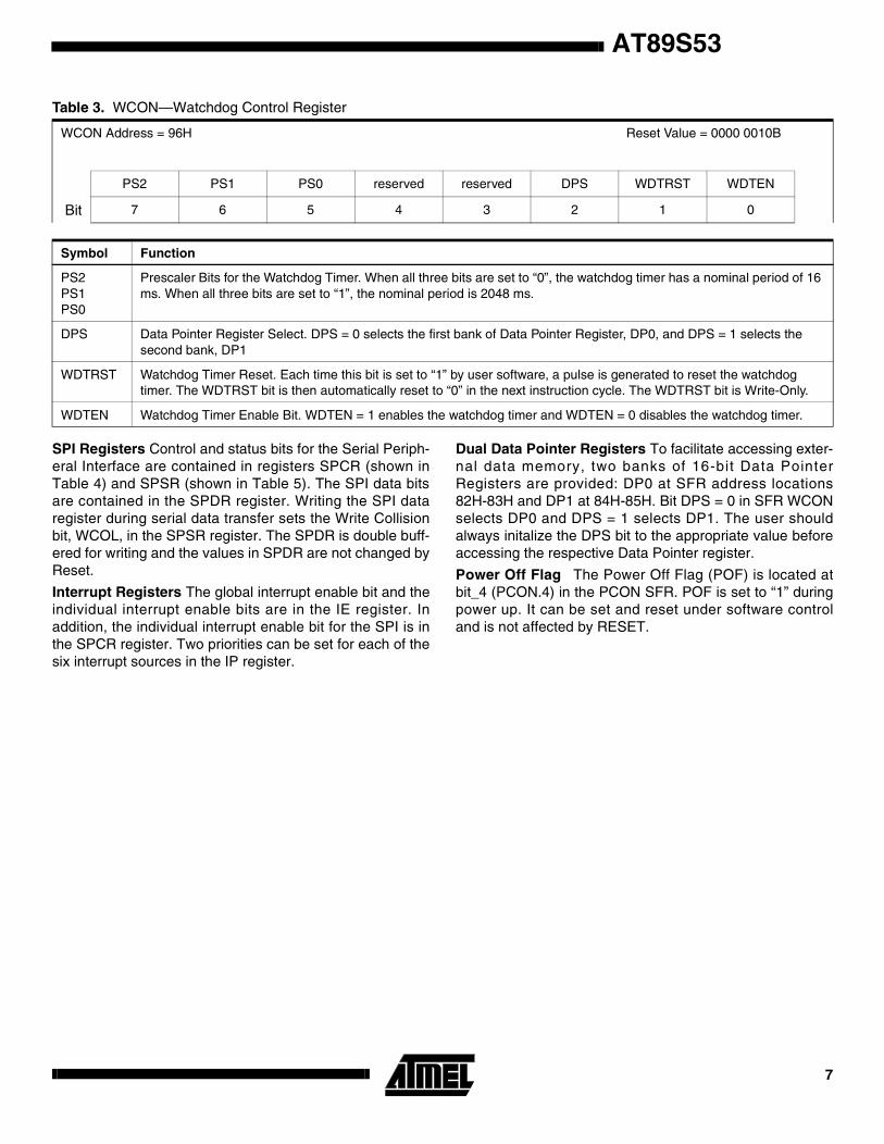
AT89S53
7
SPI Registers Control and status bits for the Serial Periph-eral Interface are contained in registers SPCR (shown inTable 4) and SPSR (shown in Table 5). The SPI data bitsare contained in the SPDR register. Writing the SPI dataregister during serial data transfer sets the Write Collisionbit, WCOL, in the SPSR register. The SPDR is double buff-ered for writing and the values in SPDR are not changed byReset.
Interrupt Registers The global interrupt enable bit and theindividual interrupt enable bits are in the IE register. Inaddition, the individual interrupt enable bit for the SPI is inthe SPCR register. Two priorities can be set for each of thesix interrupt sources in the IP register.
Dual Data Pointer Registers To facilitate accessing exter-nal data memory, two banks of 16-bit Data PointerRegisters are provided: DP0 at SFR address locations82H-83H and DP1 at 84H-85H. Bit DPS = 0 in SFR WCONselects DP0 and DPS = 1 selects DP1. The user shouldalways initalize the DPS bit to the appropriate value beforeaccessing the respective Data Pointer register.
Power Off Flag The Power Off Flag (POF) is located atbit_4 (PCON.4) in the PCON SFR. POF is set to “1” duringpower up. It can be set and reset under software controland is not affected by RESET.
Table 3. WCON—Watchdog Control Register
WCON Address = 96H Reset Value = 0000 0010B
PS2 PS1 PS0 reserved reserved DPS WDTRST WDTEN
Bit 7 6 5 4 3 2 1 0
Symbol Function
PS2PS1PS0
Prescaler Bits for the Watchdog Timer. When all three bits are set to “0”, the watchdog timer has a nominal period of 16 ms. When all three bits are set to “1”, the nominal period is 2048 ms.
DPS Data Pointer Register Select. DPS = 0 selects the first bank of Data Pointer Register, DP0, and DPS = 1 selects the second bank, DP1
WDTRST Watchdog Timer Reset. Each time this bit is set to “1” by user software, a pulse is generated to reset the watchdog timer. The WDTRST bit is then automatically reset to “0” in the next instruction cycle. The WDTRST bit is Write-Only.
WDTEN Watchdog Timer Enable Bit. WDTEN = 1 enables the watchdog timer and WDTEN = 0 disables the watchdog timer.
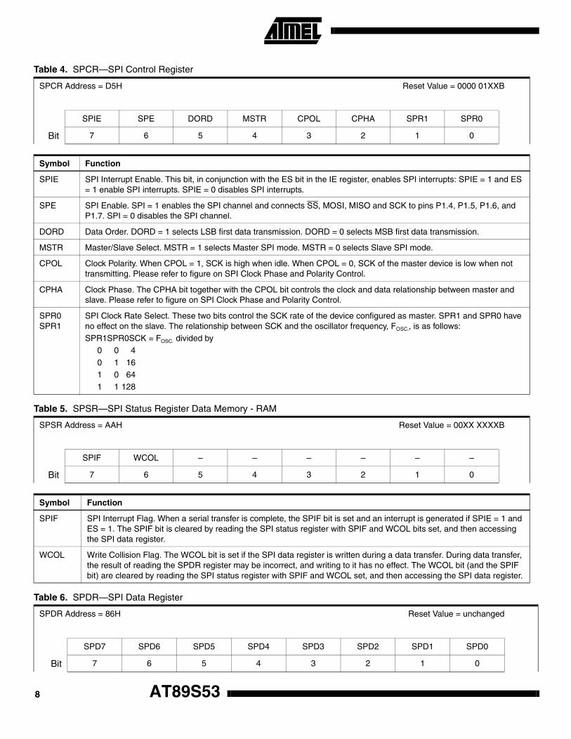
AT89S538
Table 4. SPCR—SPI Control Register
SPCR Address = D5H Reset Value = 0000 01XXB
SPIE SPE DORD MSTR CPOL CPHA SPR1 SPR0
Bit 7 6 5 4 3 2 1 0
Symbol Function
SPIE SPI Interrupt Enable. This bit, in conjunction with the ES bit in the IE register, enables SPI interrupts: SPIE = 1 and ES = 1 enable SPI interrupts. SPIE = 0 disables SPI interrupts.
SPE SPI Enable. SPI = 1 enables the SPI channel and connects SS, MOSI, MISO and SCK to pins P1.4, P1.5, P1.6, and P1.7. SPI = 0 disables the SPI channel.
DORD Data Order. DORD = 1 selects LSB first data transmission. DORD = 0 selects MSB first data transmission.
MSTR Master/Slave Select. MSTR = 1 selects Master SPI mode. MSTR = 0 selects Slave SPI mode.
CPOL Clock Polarity. When CPOL = 1, SCK is high when idle. When CPOL = 0, SCK of the master device is low when not transmitting. Please refer to figure on SPI Clock Phase and Polarity Control.
CPHA Clock Phase. The CPHA bit together with the CPOL bit controls the clock and data relationship between master and slave. Please refer to figure on SPI Clock Phase and Polarity Control.
SPR0SPR1
SPI Clock Rate Select. These two bits control the SCK rate of the device configured as master. SPR1 and SPR0 have no effect on the slave. The relationship between SCK and the oscillator frequency, FOSC., is as follows:SPR1SPR0SCK = FOSC. divided by
0 0 4
0 1 161 0 641 1 128
Table 5. SPSR—SPI Status Register Data Memory - RAM
SPSR Address = AAH Reset Value = 00XX XXXXB
SPIF WCOL – – – – – –
Bit 7 6 5 4 3 2 1 0
Symbol Function
SPIF SPI Interrupt Flag. When a serial transfer is complete, the SPIF bit is set and an interrupt is generated if SPIE = 1 and ES = 1. The SPIF bit is cleared by reading the SPI status register with SPIF and WCOL bits set, and then accessing the SPI data register.
WCOL Write Collision Flag. The WCOL bit is set if the SPI data register is written during a data transfer. During data transfer, the result of reading the SPDR register may be incorrect, and writing to it has no effect. The WCOL bit (and the SPIF bit) are cleared by reading the SPI status register with SPIF and WCOL set, and then accessing the SPI data register.
Table 6. SPDR—SPI Data Register
SPDR Address = 86H Reset Value = unchanged
SPD7 SPD6 SPD5 SPD4 SPD3 SPD2 SPD1 SPD0
Bit 7 6 5 4 3 2 1 0
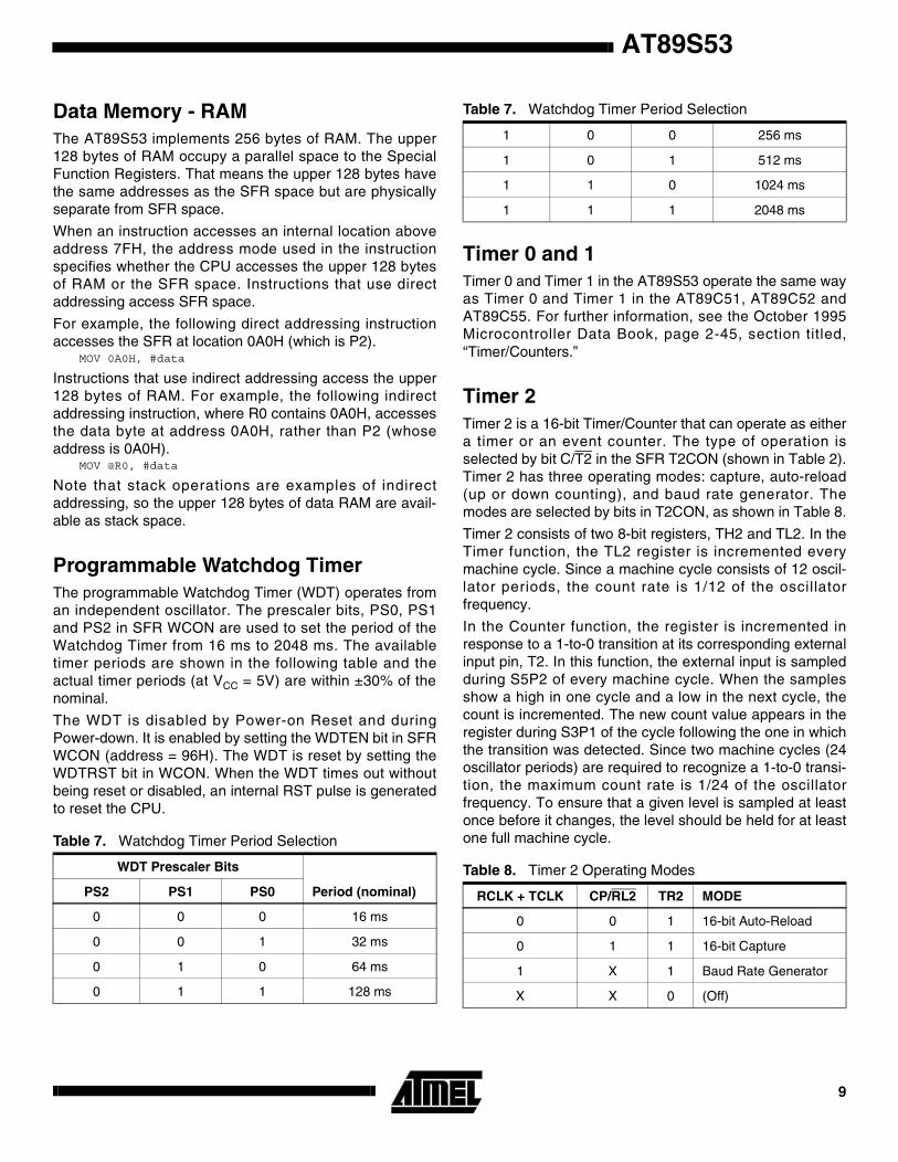
AT89S53
9
Data Memory - RAMThe AT89S53 implements 256 bytes of RAM. The upper128 bytes of RAM occupy a parallel space to the SpecialFunction Registers. That means the upper 128 bytes havethe same addresses as the SFR space but are physicallyseparate from SFR space.
When an instruction accesses an internal location aboveaddress 7FH, the address mode used in the instructionspecifies whether the CPU accesses the upper 128 bytesof RAM or the SFR space. Instructions that use directaddressing access SFR space.
For example, the following direct addressing instructionaccesses the SFR at location 0A0H (which is P2).
MOV 0A0H, #data
Instructions that use indirect addressing access the upper128 bytes of RAM. For example, the following indirectaddressing instruction, where R0 contains 0A0H, accessesthe data byte at address 0A0H, rather than P2 (whoseaddress is 0A0H).
MOV @R0, #data
Note that stack operations are examples of indirectaddressing, so the upper 128 bytes of data RAM are avail-able as stack space.
Programmable Watchdog TimerThe programmable Watchdog Timer (WDT) operates froman independent oscillator. The prescaler bits, PS0, PS1and PS2 in SFR WCON are used to set the period of theWatchdog Timer from 16 ms to 2048 ms. The availabletimer periods are shown in the following table and theactual timer periods (at VCC = 5V) are within ±30% of thenominal.
The WDT is disabled by Power-on Reset and duringPower-down. It is enabled by setting the WDTEN bit in SFRWCON (address = 96H). The WDT is reset by setting theWDTRST bit in WCON. When the WDT times out withoutbeing reset or disabled, an internal RST pulse is generatedto reset the CPU.
Timer 0 and 1Timer 0 and Timer 1 in the AT89S53 operate the same wayas Timer 0 and Timer 1 in the AT89C51, AT89C52 andAT89C55. For further information, see the October 1995Microcontroller Data Book, page 2-45, section titled,“Timer/Counters.”
Timer 2Timer 2 is a 16-bit Timer/Counter that can operate as eithera timer or an event counter. The type of operation isselected by bit C/T2 in the SFR T2CON (shown in Table 2).Timer 2 has three operating modes: capture, auto-reload(up or down counting), and baud rate generator. Themodes are selected by bits in T2CON, as shown in Table 8.
Timer 2 consists of two 8-bit registers, TH2 and TL2. In theTimer function, the TL2 register is incremented everymachine cycle. Since a machine cycle consists of 12 oscil-lator periods, the count rate is 1/12 of the oscillatorfrequency.
In the Counter function, the register is incremented inresponse to a 1-to-0 transition at its corresponding externalinput pin, T2. In this function, the external input is sampledduring S5P2 of every machine cycle. When the samplesshow a high in one cycle and a low in the next cycle, thecount is incremented. The new count value appears in theregister during S3P1 of the cycle following the one in whichthe transition was detected. Since two machine cycles (24oscillator periods) are required to recognize a 1-to-0 transi-tion, the maximum count rate is 1/24 of the oscillatorfrequency. To ensure that a given level is sampled at leastonce before it changes, the level should be held for at leastone full machine cycle.Table 7. Watchdog Timer Period Selection
WDT Prescaler Bits
Period (nominal)PS2 PS1 PS0
0 0 0 16 ms
0 0 1 32 ms
0 1 0 64 ms
0 1 1 128 ms
1 0 0 256 ms
1 0 1 512 ms
1 1 0 1024 ms
1 1 1 2048 ms
Table 8. Timer 2 Operating Modes
RCLK + TCLK CP/RL2 TR2 MODE
0 0 1 16-bit Auto-Reload
0 1 1 16-bit Capture
1 X 1 Baud Rate Generator
X X 0 (Off)
Table 7. Watchdog Timer Period Selection
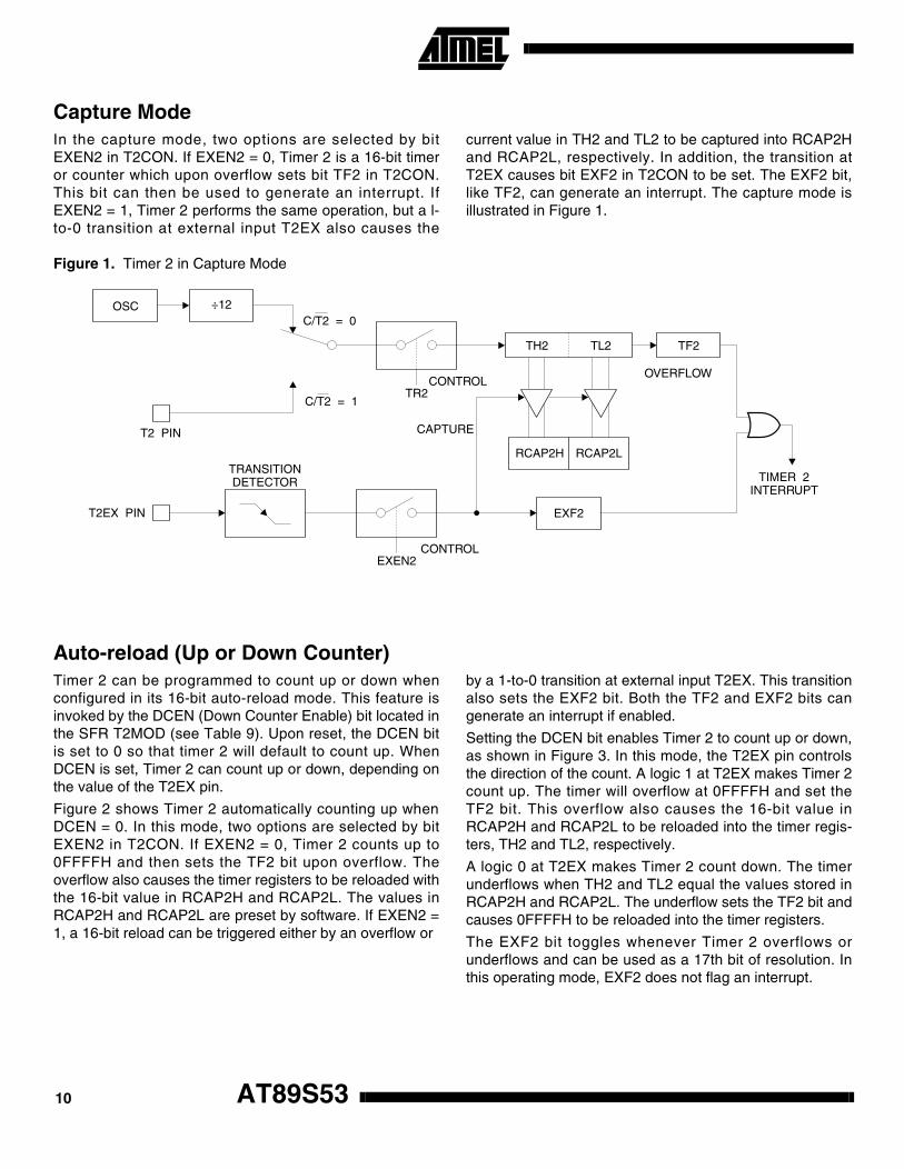
AT89S5310
Capture ModeIn the capture mode, two options are selected by bitEXEN2 in T2CON. If EXEN2 = 0, Timer 2 is a 16-bit timeror counter which upon overflow sets bit TF2 in T2CON.This bit can then be used to generate an interrupt. IfEXEN2 = 1, Timer 2 performs the same operation, but a l-to-0 transition at external input T2EX also causes the
current value in TH2 and TL2 to be captured into RCAP2Hand RCAP2L, respectively. In addition, the transition atT2EX causes bit EXF2 in T2CON to be set. The EXF2 bit,like TF2, can generate an interrupt. The capture mode isillustrated in Figure 1.
Figure 1. Timer 2 in Capture Mode
Auto-reload (Up or Down Counter)Timer 2 can be programmed to count up or down whenconfigured in its 16-bit auto-reload mode. This feature isinvoked by the DCEN (Down Counter Enable) bit located inthe SFR T2MOD (see Table 9). Upon reset, the DCEN bitis set to 0 so that timer 2 will default to count up. WhenDCEN is set, Timer 2 can count up or down, depending onthe value of the T2EX pin.
Figure 2 shows Timer 2 automatically counting up whenDCEN = 0. In this mode, two options are selected by bitEXEN2 in T2CON. If EXEN2 = 0, Timer 2 counts up to0FFFFH and then sets the TF2 bit upon overflow. Theoverflow also causes the timer registers to be reloaded withthe 16-bit value in RCAP2H and RCAP2L. The values inRCAP2H and RCAP2L are preset by software. If EXEN2 =1, a 16-bit reload can be triggered either by an overflow or
by a 1-to-0 transition at external input T2EX. This transitionalso sets the EXF2 bit. Both the TF2 and EXF2 bits cangenerate an interrupt if enabled.
Setting the DCEN bit enables Timer 2 to count up or down,as shown in Figure 3. In this mode, the T2EX pin controlsthe direction of the count. A logic 1 at T2EX makes Timer 2count up. The timer will overflow at 0FFFFH and set theTF2 bit. This overflow also causes the 16-bit value inRCAP2H and RCAP2L to be reloaded into the timer regis-ters, TH2 and TL2, respectively.
A logic 0 at T2EX makes Timer 2 count down. The timerunderflows when TH2 and TL2 equal the values stored inRCAP2H and RCAP2L. The underflow sets the TF2 bit andcauses 0FFFFH to be reloaded into the timer registers.
The EXF2 bit toggles whenever Timer 2 overflows orunderflows and can be used as a 17th bit of resolution. Inthis operating mode, EXF2 does not flag an interrupt.
OSC
EXF2T2EX PIN
T2 PIN
TR2
EXEN2
C/T2 = 0
C/T2 = 1
CONTROL
CAPTURE
OVERFLOW
CONTROL
TRANSITIONDETECTOR TIMER 2
INTERRUPT
÷12
RCAP2LRCAP2H
TH2 TL2 TF2
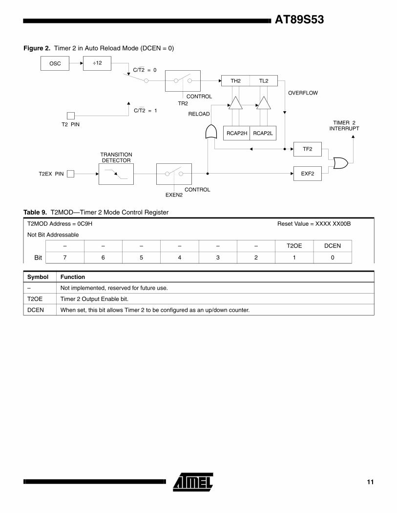
AT89S53
11
Figure 2. Timer 2 in Auto Reload Mode (DCEN = 0)
Table 9. T2MOD—Timer 2 Mode Control Register
T2MOD Address = 0C9H Reset Value = XXXX XX00B
Not Bit Addressable
– – – – – – T2OE DCEN
Bit 7 6 5 4 3 2 1 0
Symbol Function
– Not implemented, reserved for future use.
T2OE Timer 2 Output Enable bit.
DCEN When set, this bit allows Timer 2 to be configured as an up/down counter.
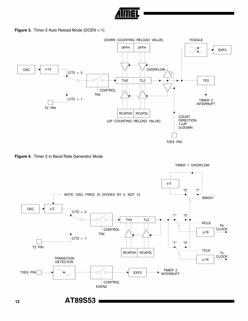
AT89S5312
Figure 3. Timer 2 Auto Reload Mode (DCEN = 1)
Figure 4. Timer 2 in Baud Rate Generator Mode
OSC
SMOD1
RCLK
TCLK
RxCLOCK
TxCLOCK
T2EX PIN
T2 PIN
TR2CONTROL
"1"
"1"
"1"
"0"
"0"
"0"
TIMER 1 OVERFLOW
NOTE: OSC. FREQ. IS DIVIDED BY 2, NOT 12
TIMER 2INTERRUPT
2
2
16
16
RCAP2LRCAP2H
TH2 TL2
C/T2 = 0
C/T2 = 1
EXF2
CONTROL
TRANSITIONDETECTOR
EXEN2
÷
÷
÷
÷
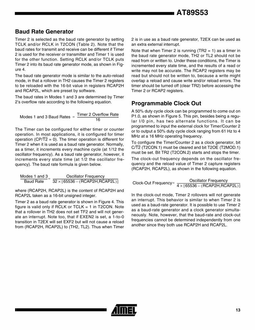
AT89S53
13
Baud Rate GeneratorTimer 2 is selected as the baud rate generator by settingTCLK and/or RCLK in T2CON (Table 2). Note that thebaud rates for transmit and receive can be different if Timer2 is used for the receiver or transmitter and Timer 1 is usedfor the other function. Setting RCLK and/or TCLK putsTimer 2 into its baud rate generator mode, as shown in Fig-ure 4.
The baud rate generator mode is similar to the auto-reloadmode, in that a rollover in TH2 causes the Timer 2 registersto be reloaded with the 16-bit value in registers RCAP2Hand RCAP2L, which are preset by software.
The baud rates in Modes 1 and 3 are determined by Timer2’s overflow rate according to the following equation.
The Timer can be configured for either timer or counteroperation. In most applications, it is configured for timeroperation (CP/T2 = 0). The timer operation is different forTimer 2 when it is used as a baud rate generator. Normally,as a timer, it increments every machine cycle (at 1/12 theoscillator frequency). As a baud rate generator, however, itincrements every state time (at 1/2 the oscillator fre-quency). The baud rate formula is given below.
where (RCAP2H, RCAP2L) is the content of RCAP2H andRCAP2L taken as a 16-bit unsigned integer.
Timer 2 as a baud rate generator is shown in Figure 4. Thisfigure is valid only if RCLK or TCLK = 1 in T2CON. Notethat a rollover in TH2 does not set TF2 and will not gener-ate an interrupt. Note too, that if EXEN2 is set, a 1-to-0transition in T2EX will set EXF2 but will not cause a reloadfrom (RCAP2H, RCAP2L) to (TH2, TL2). Thus when Timer
2 is in use as a baud rate generator, T2EX can be used asan extra external interrupt.
Note that when Timer 2 is running (TR2 = 1) as a timer inthe baud rate generator mode, TH2 or TL2 should not beread from or written to. Under these conditions, the Timer isincremented every state time, and the results of a read orwrite may not be accurate. The RCAP2 registers may beread but should not be written to, because a write mightoverlap a reload and cause write and/or reload errors. Thetimer should be turned off (clear TR2) before accessing theTimer 2 or RCAP2 registers.
Programmable Clock OutA 50% duty cycle clock can be programmed to come out onP1.0, as shown in Figure 5. This pin, besides being a regu-lar I /0 p in, has two a lternate funct ions. I t can beprogrammed to input the external clock for Timer/Counter 2or to output a 50% duty cycle clock ranging from 61 Hz to 4MHz at a 16 MHz operating frequency.
To configure the Timer/Counter 2 as a clock generator, bitC/T2 (T2CON.1) must be cleared and bit T2OE (T2MOD.1)must be set. Bit TR2 (T2CON.2) starts and stops the timer.
The clock-out frequency depends on the oscillator fre-quency and the reload value of Timer 2 capture registers(RCAP2H, RCAP2L), as shown in the following equation.
In the clock-out mode, Timer 2 rollovers will not generatean interrupt. This behavior is similar to when Timer 2 isused as a baud-rate generator. It is possible to use Timer 2as a baud-rate generator and a clock generator simulta-neously. Note, however, that the baud-rate and clock-outfrequencies cannot be determined independently from oneanother since they both use RCAP2H and RCAP2L.
Modes 1 and 3 Baud RatesTimer 2 Overflow Rate
16------------------------------------------------------------=
Modes 1 and 3Baud Rate
---------------------------------------Oscillator Frequency
32 65536 RCAP2H,RCAP2L( )–[ ]×----------------------------------------------------------------------------------------------=Clock-Out Frequency
Oscillator Frequency4 65536 RCAP2H,RCAP2L( )–[ ]×-------------------------------------------------------------------------------------------=
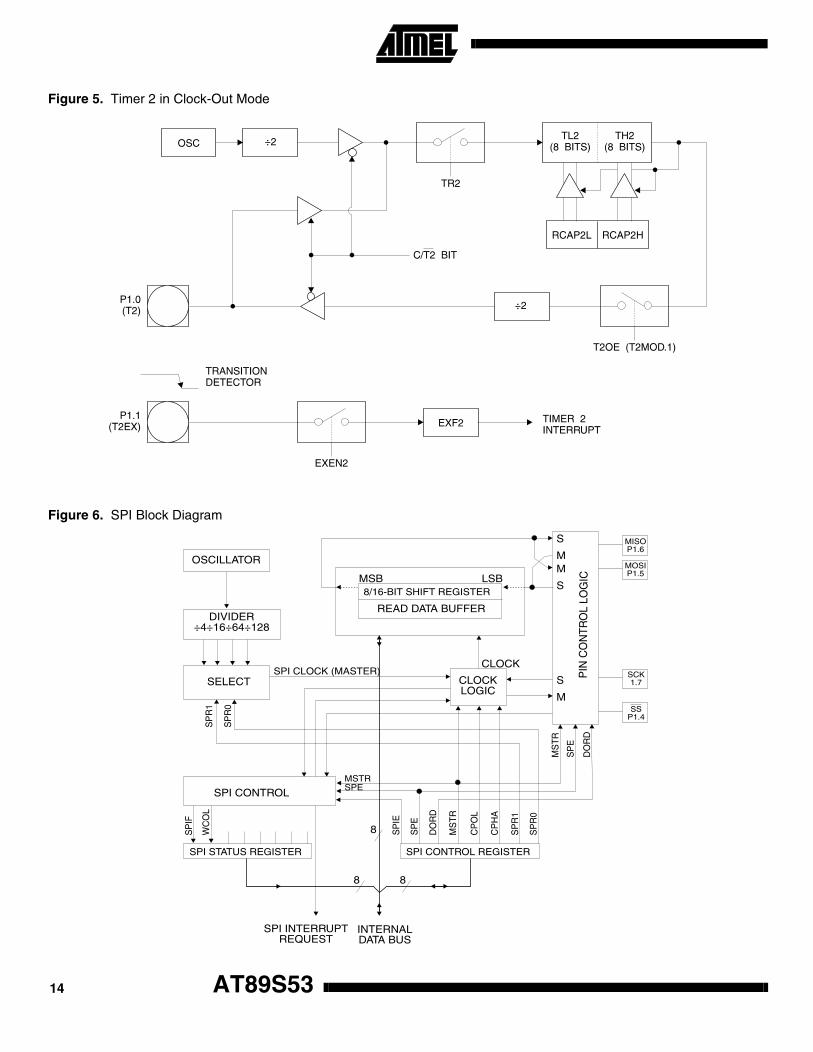
AT89S5314
Figure 5. Timer 2 in Clock-Out Mode
Figure 6. SPI Block Diagram
OSCILLATOR
8/16-BIT SHIFT REGISTER
READ DATA BUFFER
PIN
CO
NTR
OL
LOG
IC
SPI CONTROL
SPI STATUS REGISTER
SPI INTERRUPTREQUEST
INTERNALDATA BUS
SELECTSPI CLOCK (MASTER)
DIVIDER÷4÷16÷64÷128
SPI CONTROL REGISTER
8
8
8
SP
IF
WC
OL
SP
R1
MSTR
SP
IE
CLOCKLOGIC
CLOCK
MSB
S
M
SP
E
DO
RD
MS
TR
CP
OL
CP
HA
SP
R1
SP
R0
MS
TR
SP
E
DO
RD
LSB
S
MM
S
MISOP1.6
MOSIP1.5
SCK1.7
SSP1.4
SP
R0
SPE
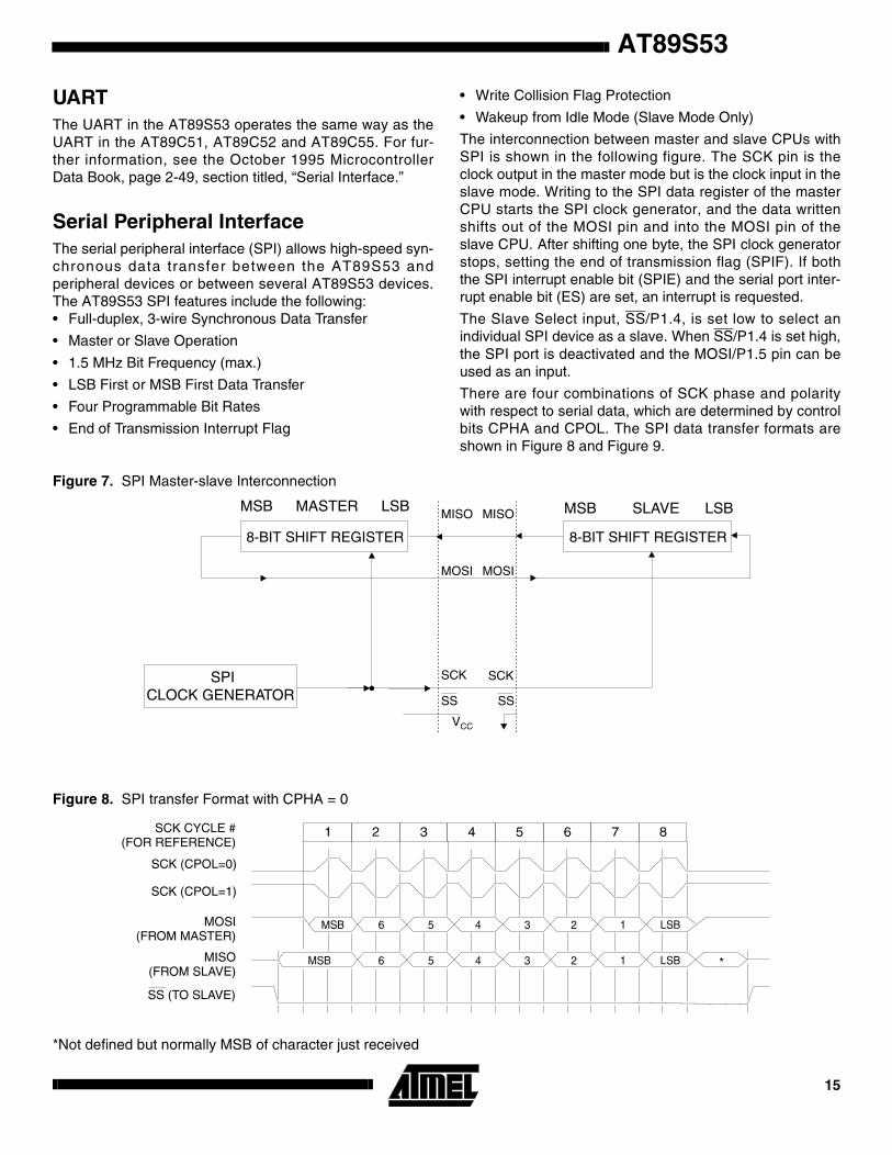
AT89S53
15
UARTThe UART in the AT89S53 operates the same way as theUART in the AT89C51, AT89C52 and AT89C55. For fur-ther information, see the October 1995 MicrocontrollerData Book, page 2-49, section titled, “Serial Interface.”
Serial Peripheral InterfaceThe serial peripheral interface (SPI) allows high-speed syn-chronous data transfer between the AT89S53 andperipheral devices or between several AT89S53 devices.The AT89S53 SPI features include the following:• Full-duplex, 3-wire Synchronous Data Transfer
• Master or Slave Operation
• 1.5 MHz Bit Frequency (max.)
• LSB First or MSB First Data Transfer
• Four Programmable Bit Rates
• End of Transmission Interrupt Flag
• Write Collision Flag Protection
• Wakeup from Idle Mode (Slave Mode Only)
The interconnection between master and slave CPUs withSPI is shown in the following figure. The SCK pin is theclock output in the master mode but is the clock input in theslave mode. Writing to the SPI data register of the masterCPU starts the SPI clock generator, and the data writtenshifts out of the MOSI pin and into the MOSI pin of theslave CPU. After shifting one byte, the SPI clock generatorstops, setting the end of transmission flag (SPIF). If boththe SPI interrupt enable bit (SPIE) and the serial port inter-rupt enable bit (ES) are set, an interrupt is requested.
The Slave Select input, SS/P1.4, is set low to select anindividual SPI device as a slave. When SS/P1.4 is set high,the SPI port is deactivated and the MOSI/P1.5 pin can beused as an input.
There are four combinations of SCK phase and polaritywith respect to serial data, which are determined by controlbits CPHA and CPOL. The SPI data transfer formats areshown in Figure 8 and Figure 9.
Figure 7. SPI Master-slave Interconnection
Figure 8. SPI transfer Format with CPHA = 0
*Not defined but normally MSB of character just received
8-BIT SHIFT REGISTER
MASTER
CLOCK GENERATORSPI
MISO
8-BIT SHIFT REGISTER
SLAVEMISO
MOSI MOSI
SCK SCK
SS SS
VCC
MSB LSB MSB LSB
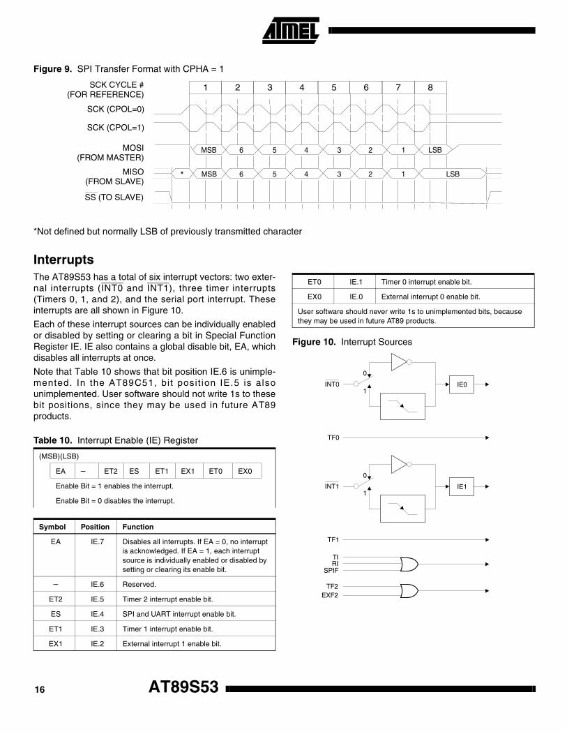
AT89S5316
Figure 9. SPI Transfer Format with CPHA = 1
*Not defined but normally LSB of previously transmitted character
InterruptsThe AT89S53 has a total of six interrupt vectors: two exter-nal interrupts (INT0 and INT1), three timer interrupts(Timers 0, 1, and 2), and the serial port interrupt. Theseinterrupts are all shown in Figure 10.
Each of these interrupt sources can be individually enabledor disabled by setting or clearing a bit in Special FunctionRegister IE. IE also contains a global disable bit, EA, whichdisables all interrupts at once.
Note that Table 10 shows that bit position IE.6 is unimple-mented. In the AT89C51, bi t posit ion IE.5 is alsounimplemented. User software should not write 1s to thesebit positions, since they may be used in future AT89products.
Figure 10. Interrupt Sources
MSB 6 5 4 3 2 1 LSB
1 2 3 4 5 6 7 8
MSB* 6 5 4 3 2 1 LSB
SCK CYCLE #(FOR REFERENCE)
SCK (CPOL=0)
SCK (CPOL=1)
MOSI(FROM MASTER)
MISO(FROM SLAVE)
SS (TO SLAVE)
Table 10. Interrupt Enable (IE) Register
(MSB)(LSB)
EA – ET2 ES ET1 EX1 ET0 EX0
Enable Bit = 1 enables the interrupt.
Enable Bit = 0 disables the interrupt.
Symbol Position Function
EA IE.7 Disables all interrupts. If EA = 0, no interrupt is acknowledged. If EA = 1, each interrupt source is individually enabled or disabled by setting or clearing its enable bit.
– IE.6 Reserved.
ET2 IE.5 Timer 2 interrupt enable bit.
ES IE.4 SPI and UART interrupt enable bit.
ET1 IE.3 Timer 1 interrupt enable bit.
EX1 IE.2 External interrupt 1 enable bit.
ET0 IE.1 Timer 0 interrupt enable bit.
EX0 IE.0 External interrupt 0 enable bit.
User software should never write 1s to unimplemented bits, because they may be used in future AT89 products.
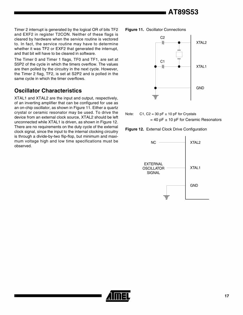
AT89S53
17
Timer 2 interrupt is generated by the logical OR of bits TF2and EXF2 in register T2CON. Neither of these flags iscleared by hardware when the service routine is vectoredto. In fact, the service routine may have to determinewhether it was TF2 or EXF2 that generated the interrupt,and that bit will have to be cleared in software.
The Timer 0 and Timer 1 flags, TF0 and TF1, are set atS5P2 of the cycle in which the timers overflow. The valuesare then polled by the circuitry in the next cycle. However,the Timer 2 flag, TF2, is set at S2P2 and is polled in thesame cycle in which the timer overflows.
Oscillator Characteristics XTAL1 and XTAL2 are the input and output, respectively,of an inverting amplifier that can be configured for use asan on-chip oscillator, as shown in Figure 11. Either a quartzcrystal or ceramic resonator may be used. To drive thedevice from an external clock source, XTAL2 should be leftunconnected while XTAL1 is driven, as shown in Figure 12.There are no requirements on the duty cycle of the externalclock signal, since the input to the internal clocking circuitryis through a divide-by-two flip-flop, but minimum and maxi-mum voltage high and low time specifications must beobserved.
Figure 11. Oscillator Connections
Note: C1, C2 = 30 pF ± 10 pF for Crystals
= 40 pF ± 10 pF for Ceramic Resonators
Figure 12. External Clock Drive Configuration
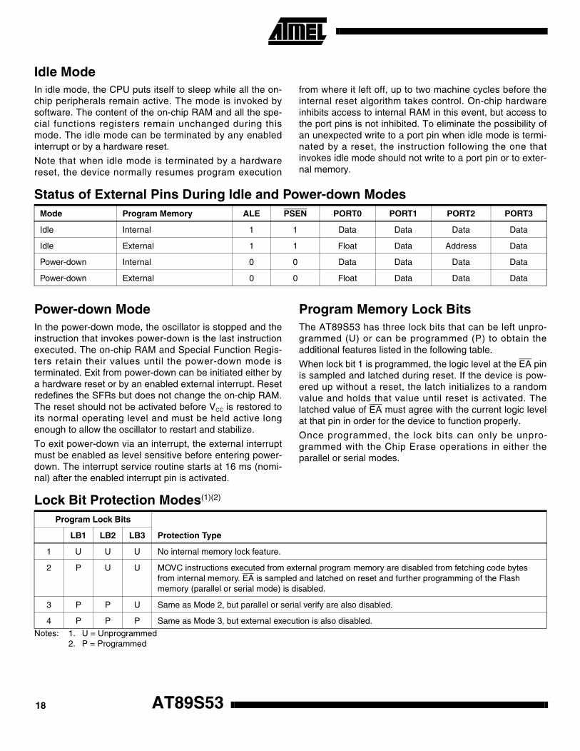
AT89S5318
Idle ModeIn idle mode, the CPU puts itself to sleep while all the on-chip peripherals remain active. The mode is invoked bysoftware. The content of the on-chip RAM and all the spe-cial functions registers remain unchanged during thismode. The idle mode can be terminated by any enabledinterrupt or by a hardware reset.
Note that when idle mode is terminated by a hardwarereset, the device normally resumes program execution
from where it left off, up to two machine cycles before theinternal reset algorithm takes control. On-chip hardwareinhibits access to internal RAM in this event, but access tothe port pins is not inhibited. To eliminate the possibility ofan unexpected write to a port pin when idle mode is termi-nated by a reset, the instruction following the one thatinvokes idle mode should not write to a port pin or to exter-nal memory.
Power-down ModeIn the power-down mode, the oscillator is stopped and theinstruction that invokes power-down is the last instructionexecuted. The on-chip RAM and Special Function Regis-ters retain their values until the power-down mode isterminated. Exit from power-down can be initiated either bya hardware reset or by an enabled external interrupt. Resetredefines the SFRs but does not change the on-chip RAM.The reset should not be activated before VCC is restored toits normal operating level and must be held active longenough to allow the oscillator to restart and stabilize.
To exit power-down via an interrupt, the external interruptmust be enabled as level sensitive before entering power-down. The interrupt service routine starts at 16 ms (nomi-nal) after the enabled interrupt pin is activated.
Program Memory Lock BitsThe AT89S53 has three lock bits that can be left unpro-grammed (U) or can be programmed (P) to obtain theadditional features listed in the following table.
When lock bit 1 is programmed, the logic level at the EA pinis sampled and latched during reset. If the device is pow-ered up without a reset, the latch initializes to a randomvalue and holds that value until reset is activated. Thelatched value of EA must agree with the current logic levelat that pin in order for the device to function properly.
Once programmed, the lock bits can only be unpro-grammed with the Chip Erase operations in either theparallel or serial modes.
Notes: 1. U = Unprogrammed2. P = Programmed
Status of External Pins During Idle and Power-down ModesMode Program Memory ALE PSEN PORT0 PORT1 PORT2 PORT3
Idle Internal 1 1 Data Data Data Data
Idle External 1 1 Float Data Address Data
Power-down Internal 0 0 Data Data Data Data
Power-down External 0 0 Float Data Data Data
Lock Bit Protection Modes(1)(2)
Program Lock Bits
Protection TypeLB1 LB2 LB3
1 U U U No internal memory lock feature.
2 P U U MOVC instructions executed from external program memory are disabled from fetching code bytes from internal memory. EA is sampled and latched on reset and further programming of the Flash memory (parallel or serial mode) is disabled.
3 P P U Same as Mode 2, but parallel or serial verify are also disabled.
4 P P P Same as Mode 3, but external execution is also disabled.
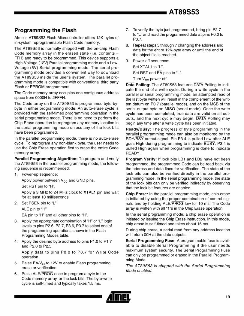
AT89S53
19
Programming the FlashAtmel’s AT89S53 Flash Microcontroller offers 12K bytes ofin-system reprogrammable Flash Code memory.
The AT89S53 is normally shipped with the on-chip FlashCode memory array in the erased state (i.e. contents =FFH) and ready to be programmed. This device supports aHigh-Voltage (12V) Parallel programming mode and a Low-Voltage (5V) Serial programming mode. The serial pro-gramming mode provides a convenient way to downloadthe AT89S53 inside the user’s system. The parallel pro-gramming mode is compatible with conventional third partyFlash or EPROM programmers.
The Code memory array occupies one contiguous addressspace from 0000H to 2FFFH.
The Code array on the AT89S53 is programmed byte-by-byte in either programming mode. An auto-erase cycle isprovided with the self-timed programming operation in theserial programming mode. There is no need to perform theChip Erase operation to reprogram any memory location inthe serial programming mode unless any of the lock bitshave been programmed.
In the parallel programming mode, there is no auto-erasecycle. To reprogram any non-blank byte, the user needs touse the Chip Erase operation first to erase the entire Codememory array.
Parallel Programming Algorithm: To program and verifythe AT89S53 in the parallel programming mode, the follow-ing sequence is recommended:
1. Power-up sequence:
Apply power between VCC and GND pins.
Set RST pin to “H”.
Apply a 3 MHz to 24 MHz clock to XTAL1 pin and waitfor at least 10 milliseconds.
2. Set PSEN pin to “L”
ALE pin to “H”
EA pin to “H” and all other pins to “H”.
3. Apply the appropriate combination of “H” or “L” logic levels to pins P2.6, P2.7, P3.6, P3.7 to select one of the programming operations shown in the Flash Programming Modes table.
4. Apply the desired byte address to pins P1.0 to P1.7 and P2.0 to P2.5.
Apply data to pins P0.0 to P0.7 for Write Codeoperation.
5. Raise EA/VPP to 12V to enable Flash programming, erase or verification.
6. Pulse ALE/PROG once to program a byte in the Code memory array, or the lock bits. The byte-write cycle is self-timed and typically takes 1.5 ms.
7. To verify the byte just programmed, bring pin P2.7 to “L” and read the programmed data at pins P0.0 to P0.7.
8. Repeat steps 3 through 7 changing the address and data for the entire 12K-byte array or until the end of the object file is reached.
9. Power-off sequence:
Set XTAL1 to “L”.
Set RST and EA pins to “L”.
Turn VCC power off.
Data Polling: The AT89S53 features DATA Polling to indi-cate the end of a write cycle. During a write cycle in theparallel or serial programming mode, an attempted read ofthe last byte written will result in the complement of the writ-ten datum on P0.7 (parallel mode), and on the MSB of theserial output byte on MISO (serial mode). Once the writecycle has been completed, true data are valid on all out-puts, and the next cycle may begin. DATA Polling maybegin any time after a write cycle has been initiated.
Ready/Busy: The progress of byte programming in theparallel programming mode can also be monitored by theRDY/BSY output signal. Pin P3.4 is pulled Low after ALEgoes High during programming to indicate BUSY. P3.4 ispulled High again when programming is done to indicateREADY.
Program Verify: If lock bits LB1 and LB2 have not beenprogrammed, the programmed Code can be read back viathe address and data lines for verification. The state of thelock bits can also be verified directly in the parallel pro-gramming mode. In the serial programming mode, the stateof the lock bits can only be verified indirectly by observingthat the lock bit features are enabled.
Chip Erase: In the parallel programming mode, chip eraseis initiated by using the proper combination of control sig-nals and by holding ALE/PROG low for 10 ms. The Codearray is written with all “1”s in the Chip Erase operation.
In the serial programming mode, a chip erase operation isinitiated by issuing the Chip Erase instruction. In this mode,chip erase is self-timed and takes about 16 ms.
During chip erase, a serial read from any address locationwill return 00H at the data outputs.
Serial Programming Fuse: A programmable fuse is avail-able to disable Serial Programming if the user needsmaximum system security. The Serial Programming Fusecan only be programmed or erased in the Parallel Program-ming Mode.
The AT89S53 is shipped with the Serial ProgrammingMode enabled.
AT89S5320
Reading the Signature Bytes: The signature bytes areread by the same procedure as a normal verification oflocations 030H and 031H, except that P3.6 and P3.7 mustbe pulled to a logic low. The values returned are as follows:
(030H) = 1EH indicates manufactured by Atmel(031H) = 53H indicates 89S53
Programming InterfaceEvery code byte in the Flash array can be written, and theentire array can be erased, by using the appropriate combi-nation of control signals. The write operation cycle is self-timed and once initiated, will automatically time itself tocompletion.
All major programming vendors offer worldwide support forthe Atmel microcontroller series. Please contact your localprogramming vendor for the appropriate software revision.
Serial DownloadingThe Code memory array can be programmed using theserial SPI bus while RST is pulled to VCC. The serial inter-face consists of pins SCK, MOSI (input) and MISO (output).After RST is set high, the Programming Enable instructionneeds to be executed first before program/erase operationscan be executed.
An auto-erase cycle is built into the self-timed programmingoperation (in the serial mode ONLY) and there is no needto first execute the Chip Erase instruction unless any of thelock bits have been programmed. The Chip Erase opera-tion turns the content of every memory location in the Codearray into FFH.
The Code memory array has an address space of 0000H to2FFFH.
Either an external system clock is supplied at pin XTAL1 or a crystal needs to be connected across pins XTAL1 and XTAL2. The maximum serial clock (SCK) frequency should
be less than 1/40 of the crystal frequency. With a 24 MHz oscillator clock, the maximum SCK frequency is 600 kHz.
Serial Programming AlgorithmTo program and verify the AT89S53 in the serial program-ming mode, the following sequence is recommended:
1. Power-up sequence:
Apply power between VCC and GND pins.
Set RST pin to “H”.
If a crystal is not connected across pins XTAL1 andXTAL2, apply a 3 MHz to 24 MHz clock to XTAL1 pinand wait for at least 10 milliseconds.
2. Enable serial programming by sending the Pro-gramming Enable serial instruction to pin MOSI/P1.5. The frequency of the shift clock sup-plied at pin SCK/P1.7 needs to be less than the CPU clock at XTAL1 divided by 40.
3. The Code array is programmed one byte at a time by supplying the address and data together with the appropriate Write instruction. The selected memory location is first automatically erased before new data is written. The write cycle is self-timed and typ-ically takes less than 2.5 ms at 5V.
4. Any memory location can be verified by using the Read instruction which returns the content at the selected address at serial output MISO/P1.6.
5. At the end of a programming session, RST can be set low to commence normal operation.
Power-off sequence (if needed):
Set XTAL1 to “L” (if a crystal is not used).
Set RST to “L”.
Turn VCC power off.
Serial Programming InstructionThe Instruction Set for Serial Programming follows a 3 byteprotocol and is shown in the following table.
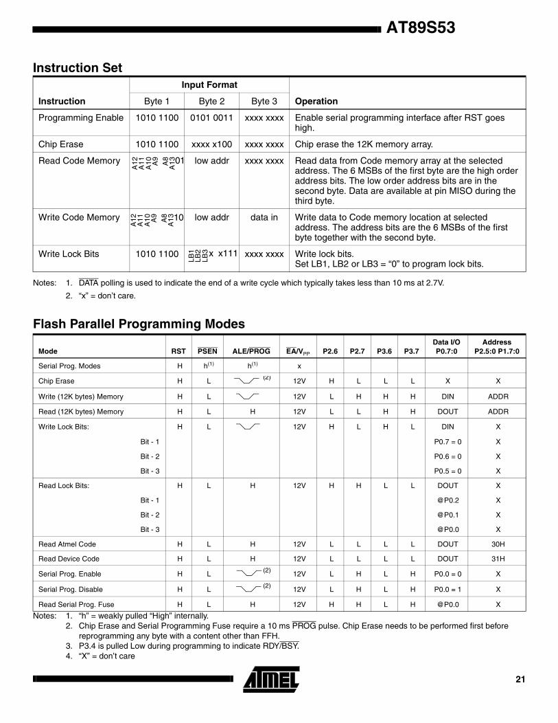
AT89S53
21
.
Notes: 1. “h” = weakly pulled “High” internally.2. Chip Erase and Serial Programming Fuse require a 10 ms PROG pulse. Chip Erase needs to be performed first before
reprogramming any byte with a content other than FFH.3. P3.4 is pulled Low during programming to indicate RDY/BSY.4. “X” = don’t care
Flash Parallel Programming Modes
Mode RST PSEN ALE/PROG EA/VPP P2.6 P2.7 P3.6 P3.7Data I/O P0.7:0
Address P2.5:0 P1.7:0
Serial Prog. Modes H h(1) h(1) x
Chip Erase H L 12V H L L L X X
Write (12K bytes) Memory H L 12V L H H H DIN ADDR
Read (12K bytes) Memory H L H 12V L L H H DOUT ADDR
Write Lock Bits: H L 12V H L H L DIN X
Bit - 1 P0.7 = 0 X
Bit - 2 P0.6 = 0 X
Bit - 3 P0.5 = 0 X
Read Lock Bits: H L H 12V H H L L DOUT X
Bit - 1 @P0.2 X
Bit - 2 @P0.1 X
Bit - 3 @P0.0 X
Read Atmel Code H L H 12V L L L L DOUT 30H
Read Device Code H L H 12V L L L L DOUT 31H
Serial Prog. Enable H L 12V L H L H P0.0 = 0 X
Serial Prog. Disable H L 12V L H L H P0.0 = 1 X
Read Serial Prog. Fuse H L H 12V H H L H @P0.0 X
(2)
(2)
(2)
Instruction Set
Notes: 1. DATA polling is used to indicate the end of a write cycle which typically takes less than 10 ms at 2.7V.
2. “x” = don’t care.
Instruction
Input Format
OperationByte 1 Byte 2 Byte 3
Programming Enable 1010 1100 0101 0011 xxxx xxxx Enable serial programming interface after RST goes high.
Chip Erase 1010 1100 xxxx x100 xxxx xxxx Chip erase the 12K memory array.
Read Code Memory low addr xxxx xxxx Read data from Code memory array at the selected address. The 6 MSBs of the first byte are the high order address bits. The low order address bits are in the second byte. Data are available at pin MISO during the third byte.
Write Code Memory low addr data in Write data to Code memory location at selected address. The address bits are the 6 MSBs of the first byte together with the second byte.
Write Lock Bits 1010 1100 xxxx xxxx Write lock bits.Set LB1, LB2 or LB3 = “0” to program lock bits.
A12
A11
A10 A
9A
8A
1301
A12
A11
A10 A
9A
8A
1310
LB1
LB2
LB3 x x111
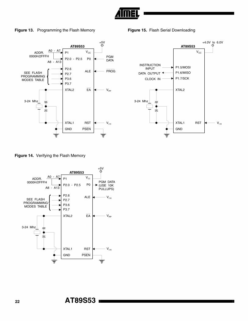
AT89S5322
Figure 13. Programming the Flash Memory
Figure 14. Verifying the Flash Memory
Figure 15. Flash Serial Downloading
P1
P2.6
P3.6
P2.0 - P2.5
A0 - A7ADDR.
0000H/2FFFH
SEE FLASHPROGRAMMINGMODES TABLE
3-24 Mhz
A8 - A13P0
+5V
P2.7
PGMDATA
PROG
VPP
VI H
ALE
P3.7
XTAL2 EA
RST
PSEN
XTAL1
GND
VCC
AT89S53
P1
P2.6
P3.6
P2.0 - P2.5
A0 - A7ADDR.
0000H/2FFFH
SEE FLASHPROGRAMMINGMODES TABLE
3-24 Mhz
A8 - A13P0
+5V
P2.7
PGM DATA(USE 10KPULLUPS)
VI H
VI HALE
P3.7
XTAL2 EA
RST
PSEN
XTAL1
GND
VCC
AT89S53
VPP
P1.7/SCK
DATA OUTPUT
INSTRUCTIONINPUT
CLOCK IN
3-24 Mhz
+4.0V to 6.0V
P1.5/MOSI
VI H
XTAL2
RSTXTAL1
GND
VCC
AT89S53
P1.6/MISO
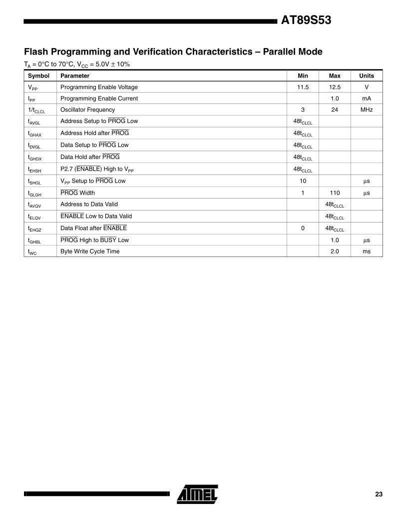
AT89S53
23
Flash Programming and Verification Characteristics – Parallel ModeTA = 0°C to 70°C, VCC = 5.0V ± 10%
Symbol Parameter Min Max Units
VPP Programming Enable Voltage 11.5 12.5 V
IPP Programming Enable Current 1.0 mA
1/tCLCL Oscillator Frequency 3 24 MHz
tAVGL Address Setup to PROG Low 48tCLCL
tGHAX Address Hold after PROG 48tCLCL
tDVGL Data Setup to PROG Low 48tCLCL
tGHDX Data Hold after PROG 48tCLCL
tEHSH P2.7 (ENABLE) High to VPP 48tCLCL
tSHGL VPP Setup to PROG Low 10 µs
tGLGH PROG Width 1 110 µs
tAVQV Address to Data Valid 48tCLCL
tELQV ENABLE Low to Data Valid 48tCLCL
tEHQZ Data Float after ENABLE 0 48tCLCL
tGHBL PROG High to BUSY Low 1.0 µs
tWC Byte Write Cycle Time 2.0 ms
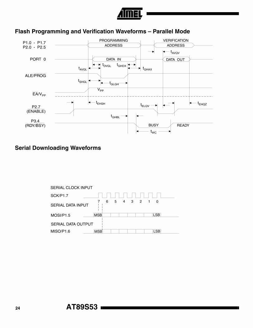
AT89S5324
Flash Programming and Verification Waveforms – Parallel Mode
Serial Downloading Waveforms
SERIAL CLOCK INPUT
SERIAL DATA INPUT
SCK/P1.7
MOSI/P1.5
MISO/P1.6
SERIAL DATA OUTPUT
01234567
MSB
MSB
LSB
LSB
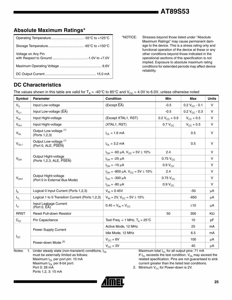
AT89S53
25
Notes: 1. Under steady state (non-transient) conditions, IOL must be externally limited as follows:Maximum IOL per port pin: 10 mAMaximum IOL per 8-bit port:Port 0: 26 mAPorts 1,2, 3: 15 mA
Maximum total IOL for all output pins: 71 mAIf IOL exceeds the test condition, VOL may exceed the related specification. Pins are not guaranteed to sink current greater than the listed test conditions.
2. Minimum VCC for Power-down is 2V.
Absolute Maximum Ratings*Operating Temperature.................................. -55°C to +125°C *NOTICE: Stresses beyond those listed under “Absolute
Maximum Ratings” may cause permanent dam-age to the device. This is a stress rating only and functional operation of the device at these or any other conditions beyond those indicated in the operational sections of this specification is not implied. Exposure to absolute maximum rating conditions for extended periods may affect device reliability.
Storage Temperature ..................................... -65°C to +150°C
Voltage on Any Pinwith Respect to Ground .....................................-1.0V to +7.0V
Maximum Operating Voltage ............................................ 6.6V
DC Output Current...................................................... 15.0 mA
DC CharacteristicsThe values shown in this table are valid for TA = -40°C to 85°C and VCC = 4.0V to 6.0V, unless otherwise noted
Symbol Parameter Condition Min Max Units
VIL Input Low-voltage (Except EA) -0.5 0.2 VCC - 0.1 V
VIL1 Input Low-voltage (EA) -0.5 0.2 VCC - 0.3 V
VIH Input Hight-voltage (Except XTAL1, RST) 0.2 VCC + 0.9 VCC + 0.5 V
VIH1 Input Hight-voltage (XTAL1, RST) 0.7 VCC VCC + 0.5 V
VOLOutput Low-voltage (1)
(Ports 1,2,3)IOL = 1.6 mA 0.5 V
VOL1Output Low-voltage (1)
(Port 0, ALE, PSEN)IOL = 3.2 mA 0.5 V
VOHOutput Hight-voltage(Ports 1,2,3, ALE, PSEN)
IOH = -60 µA, VCC = 5V ± 10% 2.4 V
IOH = -25 µA 0.75 VCC V
IOH = -10 µA 0.9 VCC V
VOH1Output Hight-voltage(Port 0 in External Bus Mode)
IOH = -800 µA, VCC = 5V ± 10% 2.4 V
IOH = -300 µA 0.75 VCC V
IOH = -80 µA 0.9 VCC V
IIL Logical 0 Input Current (Ports 1,2,3) VIN = 0.45V -50 µA
ITL Logical 1 to 0 Transition Current (Ports 1,2,3) VIN = 2V, VCC = 5V ± 10% -650 µA
ILIInput Leakage Current (Port 0, EA) 0.45 < VIN < VCC ±10 µA
RRST Reset Pull-down Resistor 50 300 KΩ
CIO Pin Capacitance Test Freq. = 1 MHz, TA = 25°C 10 pF
ICC
Power Supply CurrentActive Mode, 12 MHz 25 mA
Idle Mode, 12 MHz 6.5 mA
Power-down Mode (2)VCC = 6V 100 µA
VCC = 3V 40 µA
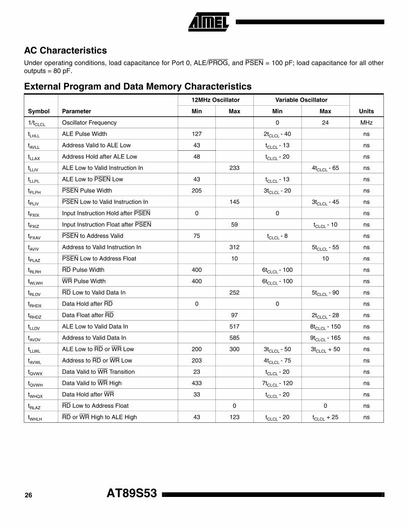
AT89S5326
AC Characteristics Under operating conditions, load capacitance for Port 0, ALE/PROG, and PSEN = 100 pF; load capacitance for all otheroutputs = 80 pF.
External Program and Data Memory Characteristics
Symbol Parameter
12MHz Oscillator Variable Oscillator
UnitsMin Max Min Max
1/tCLCL Oscillator Frequency 0 24 MHz
tLHLL ALE Pulse Width 127 2tCLCL - 40 ns
tAVLL Address Valid to ALE Low 43 tCLCL - 13 ns
tLLAX Address Hold after ALE Low 48 tCLCL - 20 ns
tLLIV ALE Low to Valid Instruction In 233 4tCLCL - 65 ns
tLLPL ALE Low to PSEN Low 43 tCLCL - 13 ns
tPLPH PSEN Pulse Width 205 3tCLCL - 20 ns
tPLIV PSEN Low to Valid Instruction In 145 3tCLCL - 45 ns
tPXIX Input Instruction Hold after PSEN 0 0 ns
tPXIZ Input Instruction Float after PSEN 59 tCLCL - 10 ns
tPXAV PSEN to Address Valid 75 tCLCL - 8 ns
tAVIV Address to Valid Instruction In 312 5tCLCL - 55 ns
tPLAZ PSEN Low to Address Float 10 10 ns
tRLRH RD Pulse Width 400 6tCLCL - 100 ns
tWLWH WR Pulse Width 400 6tCLCL - 100 ns
tRLDV RD Low to Valid Data In 252 5tCLCL - 90 ns
tRHDX Data Hold after RD 0 0 ns
tRHDZ Data Float after RD 97 2tCLCL - 28 ns
tLLDV ALE Low to Valid Data In 517 8tCLCL - 150 ns
tAVDV Address to Valid Data In 585 9tCLCL - 165 ns
tLLWL ALE Low to RD or WR Low 200 300 3tCLCL - 50 3tCLCL + 50 ns
tAVWL Address to RD or WR Low 203 4tCLCL - 75 ns
tQVWX Data Valid to WR Transition 23 tCLCL - 20 ns
tQVWH Data Valid to WR High 433 7tCLCL - 120 ns
tWHQX Data Hold after WR 33 tCLCL - 20 ns
tRLAZ RD Low to Address Float 0 0 ns
tWHLH RD or WR High to ALE High 43 123 tCLCL - 20 tCLCL + 25 ns
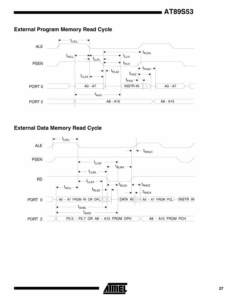
AT89S53
27
External Program Memory Read Cycle
External Data Memory Read Cycle
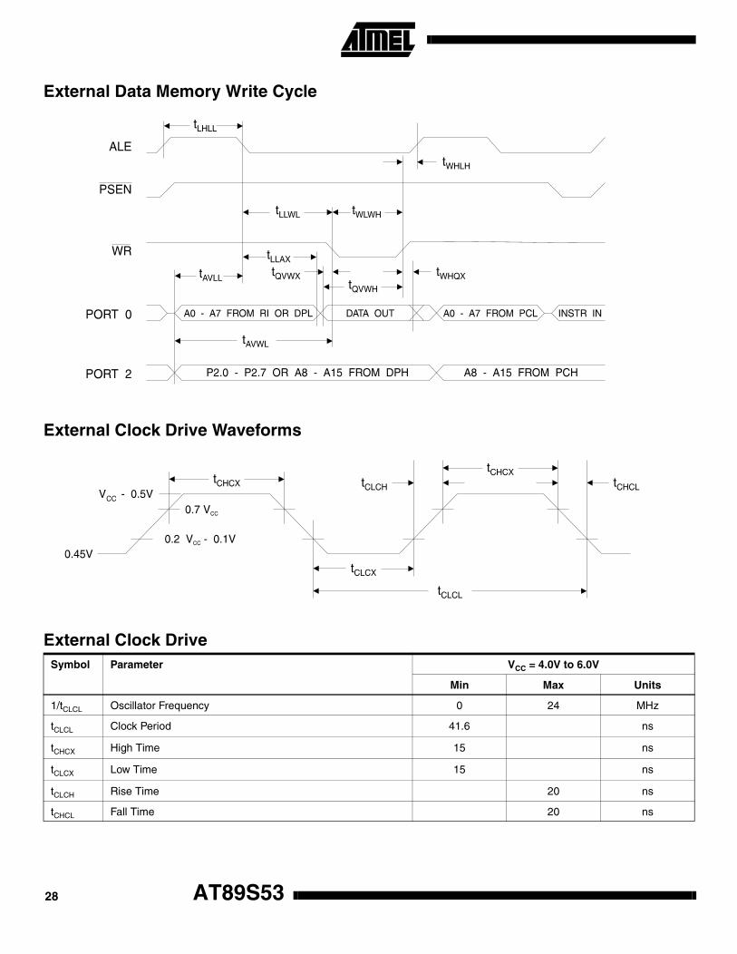
AT89S5328
External Data Memory Write Cycle
External Clock Drive Waveforms
External Clock DriveSymbol Parameter VCC = 4.0V to 6.0V
Min Max Units
1/tCLCL Oscillator Frequency 0 24 MHz
tCLCL Clock Period 41.6 ns
tCHCX High Time 15 ns
tCLCX Low Time 15 ns
tCLCH Rise Time 20 ns
tCHCL Fall Time 20 ns
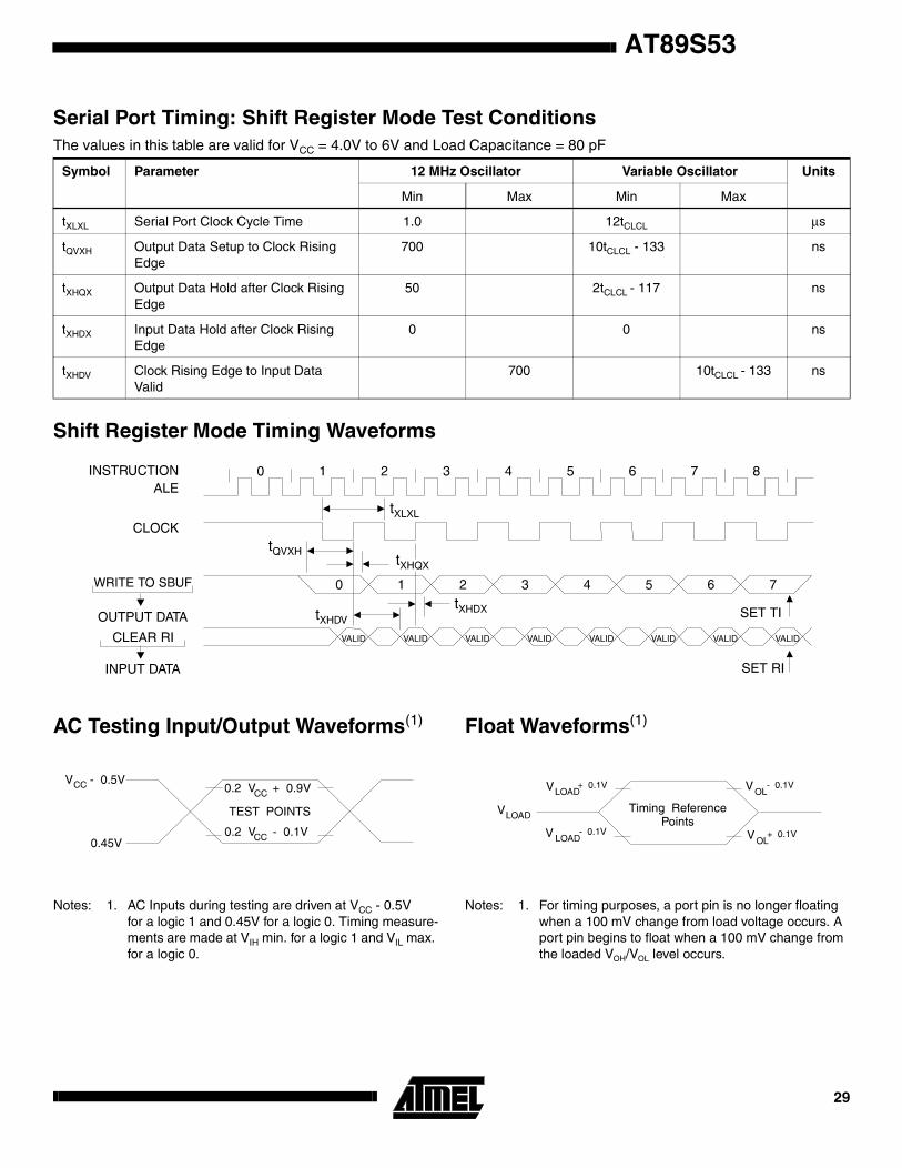
AT89S53
29
.
Shift Register Mode Timing Waveforms
AC Testing Input/Output Waveforms(1)
Notes: 1. AC Inputs during testing are driven at VCC - 0.5V for a logic 1 and 0.45V for a logic 0. Timing measure-ments are made at VIH min. for a logic 1 and VIL max. for a logic 0.
Float Waveforms(1)
Notes: 1. For timing purposes, a port pin is no longer floating when a 100 mV change from load voltage occurs. A port pin begins to float when a 100 mV change from the loaded VOH/VOL level occurs.
Serial Port Timing: Shift Register Mode Test ConditionsThe values in this table are valid for VCC = 4.0V to 6V and Load Capacitance = 80 pF
Symbol Parameter 12 MHz Oscillator Variable Oscillator Units
Min Max Min Max
tXLXL Serial Port Clock Cycle Time 1.0 12tCLCL µs
tQVXH Output Data Setup to Clock Rising Edge
700 10tCLCL - 133 ns
tXHQX Output Data Hold after Clock Rising Edge
50 2tCLCL - 117 ns
tXHDX Input Data Hold after Clock Rising Edge
0 0 ns
tXHDV Clock Rising Edge to Input Data Valid
700 10tCLCL - 133 ns
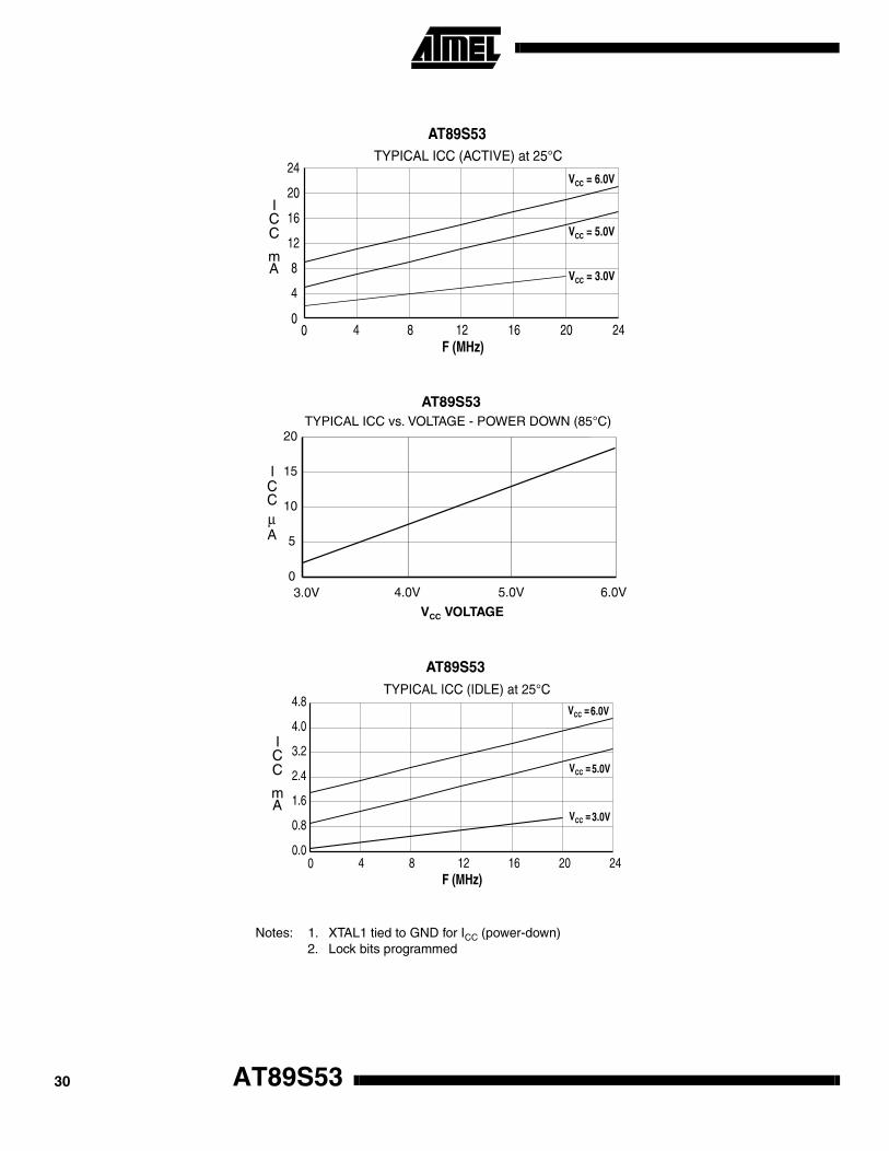
AT89S5330
Notes: 1. XTAL1 tied to GND for ICC (power-down)2. Lock bits programmed
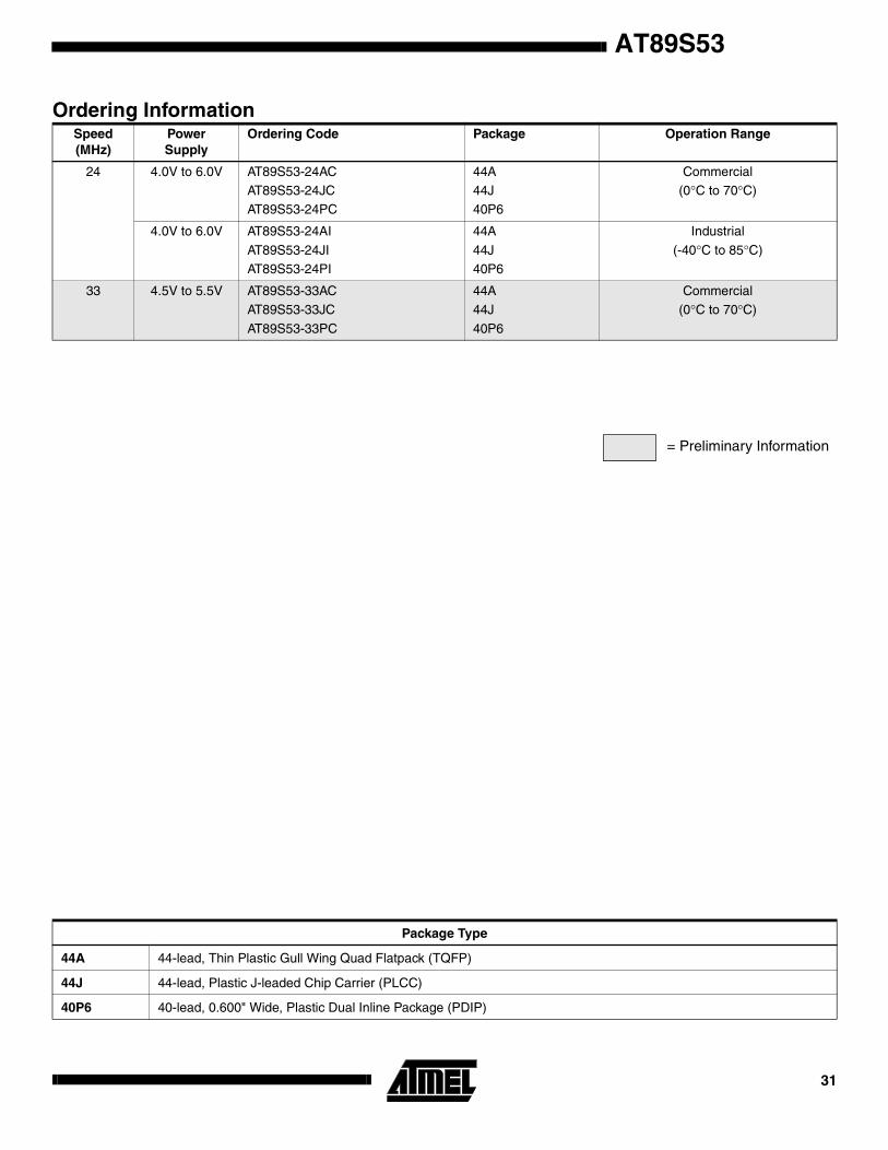
AT89S53
31
Ordering InformationSpeed(MHz)
PowerSupply
Ordering Code Package Operation Range
24 4.0V to 6.0V AT89S53-24ACAT89S53-24JCAT89S53-24PC
44A44J40P6
Commercial(0°C to 70°C)
4.0V to 6.0V AT89S53-24AI
AT89S53-24JIAT89S53-24PI
44A
44J40P6
Industrial
(-40°C to 85°C)
33 4.5V to 5.5V AT89S53-33ACAT89S53-33JC
AT89S53-33PC
44A44J
40P6
Commercial(0°C to 70°C)
Package Type
44A 44-lead, Thin Plastic Gull Wing Quad Flatpack (TQFP)
44J 44-lead, Plastic J-leaded Chip Carrier (PLCC)
40P6 40-lead, 0.600" Wide, Plastic Dual Inline Package (PDIP)
= Preliminary Information
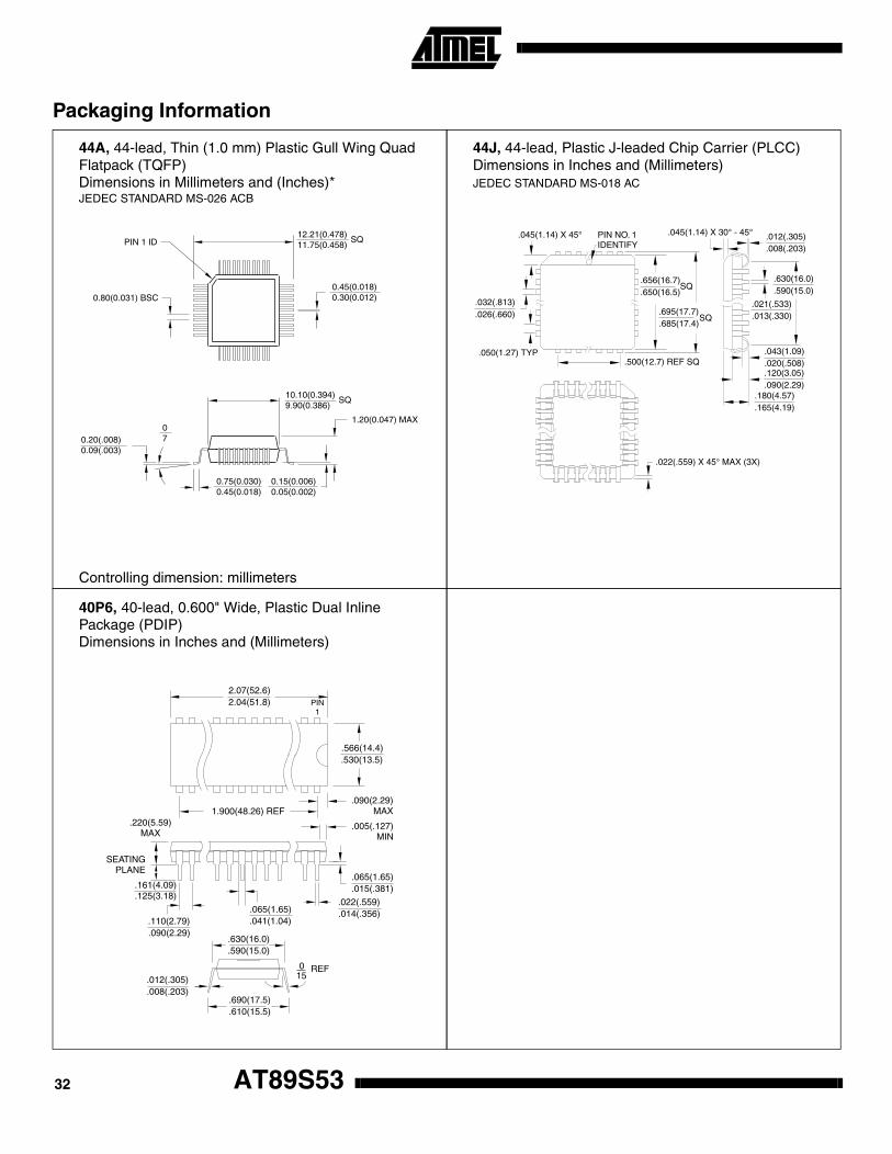
AT89S5332
Packaging Information
Controlling dimension: millimeters
1.20(0.047) MAX
10.10(0.394)9.90(0.386)
SQ
12.21(0.478)11.75(0.458)
SQ
0.75(0.030)0.45(0.018)
0.15(0.006)0.05(0.002)
0.20(.008)0.09(.003)
07
0.80(0.031) BSC
PIN 1 ID
0.45(0.018)0.30(0.012)
.045(1.14) X 45° PIN NO. 1IDENTIFY
.045(1.14) X 30° - 45° .012(.305).008(.203)
.021(.533)
.013(.330)
.630(16.0)
.590(15.0)
.043(1.09)
.020(.508)
.120(3.05)
.090(2.29).180(4.57).165(4.19)
.500(12.7) REF SQ
.032(.813)
.026(.660)
.050(1.27) TYP
.022(.559) X 45° MAX (3X)
.656(16.7)
.650(16.5)
.695(17.7)
.685(17.4)SQ
SQ
2.07(52.6)2.04(51.8) PIN
1
.566(14.4)
.530(13.5)
.090(2.29)MAX
.005(.127)MIN
.065(1.65)
.015(.381)
.022(.559)
.014(.356).065(1.65).041(1.04)
015
REF
.690(17.5)
.610(15.5)
.630(16.0)
.590(15.0)
.012(.305)
.008(.203)
.110(2.79)
.090(2.29)
.161(4.09)
.125(3.18)
SEATINGPLANE
.220(5.59)MAX
1.900(48.26) REF
44A, 44-lead, Thin (1.0 mm) Plastic Gull Wing Quad Flatpack (TQFP)Dimensions in Millimeters and (Inches)*JEDEC STANDARD MS-026 ACB
44J, 44-lead, Plastic J-leaded Chip Carrier (PLCC)Dimensions in Inches and (Millimeters)JEDEC STANDARD MS-018 AC
40P6, 40-lead, 0.600" Wide, Plastic Dual Inline Package (PDIP)Dimensions in Inches and (Millimeters)
© Atmel Corporation 2000.Atmel Corporation makes no warranty for the use of its products, other than those expressly contained in the Company’s standard war-ranty which is detailed in Atmel’s Terms and Conditions located on the Company’s web site. The Company assumes no responsibility forany errors which may appear in this document, reserves the right to change devices or specifications detailed herein at any time withoutnotice, and does not make any commitment to update the information contained herein. No licenses to patents or other intellectual prop-erty of Atmel are granted by the Company in connection with the sale of Atmel products, expressly or by implication. Atmel’s products arenot authorized for use as critical components in life support devices or systems.
Atmel Headquarters Atmel Operations
Corporate Headquarters2325 Orchard ParkwaySan Jose, CA 95131TEL (408) 441-0311FAX (408) 487-2600
EuropeAtmel U.K., Ltd.Coliseum Business CentreRiverside WayCamberley, Surrey GU15 3YLEnglandTEL (44) 1276-686-677FAX (44) 1276-686-697
AsiaAtmel Asia, Ltd.Room 1219Chinachem Golden Plaza77 Mody Road TsimhatsuiEast KowloonHong KongTEL (852) 2721-9778FAX (852) 2722-1369
JapanAtmel Japan K.K.9F, Tonetsu Shinkawa Bldg.1-24-8 ShinkawaChuo-ku, Tokyo 104-0033JapanTEL (81) 3-3523-3551FAX (81) 3-3523-7581
Atmel Colorado Springs1150 E. Cheyenne Mtn. Blvd.Colorado Springs, CO 80906TEL (719) 576-3300FAX (719) 540-1759
Atmel RoussetZone Industrielle13106 Rousset CedexFranceTEL (33) 4-4253-6000FAX (33) 4-4253-6001
Fax-on-DemandNorth America:1-(800) 292-8635
International:1-(408) 441-0732
Web Sitehttp://www.atmel.com
BBS1-(408) 436-4309
Printed on recycled paper.
0787D–06/00/xM
Marks bearing ® and/or ™ are registered trademarks and trademarks of Atmel Corporation.
Terms and product names in this document may be trademarks of others.
FUNCTIONAL BLOCK DIAGRAM
PGABUFFER
CHARGE BALANCINGA/D CONVERTER
SIGMA-DELTAMODULATOR
DIGITALFILTER
REF IN(–) REF IN(+) AVDD DVDD
A = 1–128 MCLK INMCLK OUT
RESET
AIN(+)
AIN(–)
SERIALINTERFACE
REGISTER BANKSCLKCSDINDOUTDRDY
CLOCKGENERATION
AGND DGND
AD7715
REV. C
Information furnished by Analog Devices is believed to be accurate andreliable. However, no responsibility is assumed by Analog Devices for itsuse, nor for any infringements of patents or other rights of third partieswhich may result from its use. No license is granted by implication orotherwise under any patent or patent rights of Analog Devices.
a 3 V/5 V, 450 mA16-Bit, Sigma-Delta ADC
AD7715*FEATURES
Charge-Balancing ADC
16 Bits No Missing Codes
0.0015% Nonlinearity
Programmable Gain Front End
Gains of 1, 2, 32 and 128
Differential Input Capability
Three-Wire Serial Interface
SPI™, QSPI™, MICROWIRE™ and DSP Compatible
Ability to Buffer the Analog Input
3 V (AD7715-3) or 5 V (AD7715-5) Operation
Low Supply Current: 450 mA max @ 3 V Supplies
Low-Pass Filter with Programmable Output Update
16-Lead SOIC/DIP/TSSOP
CMOS construction ensures very low power dissipation, and thepower-down mode reduces the standby power consumption to50 µW typ. The part is available in a 16-lead, 0.3 inch-wide,plastic dual-in-line package (DIP) as well as a 16-lead 0.3 inch-wide small outline (SOIC) package and a 16-lead TSSOP package.
PRODUCT HIGHLIGHTS1. The AD7715 consumes less than 450 µA in total supply
current at 3 V supplies and 1 MHz master clock, making itideal for use in low-power systems. Standby current is lessthan 10 µA.
2. The programmable gain input allows the AD7715 to acceptinput signals directly from a strain gage or transducer remov-ing a considerable amount of signal conditioning.
3. The AD7715 is ideal for microcontroller or DSP processorapplications with a three-wire serial interface reducing thenumber of interconnect lines and reducing the number ofopto-couplers required in isolated systems. The part con-tains on-chip registers which allow software control overoutput update rate, input gain, signal polarity and calibrationmodes.
4. The part features excellent static performance specificationswith 16-bits no missing codes, ±0.0015% accuracy and lowrms noise (<550 nV). Endpoint errors and the effects oftemperature drift are eliminated by on-chip calibration op-tions, which remove zero-scale and full-scale errors.
GENERAL DESCRIPTIONThe AD7715 is a complete analog front end for low frequencymeasurement applications. The part can accept low level inputsignals directly from a transducer and outputs a serial digitalword. It employs a sigma-delta conversion technique to realizeup to 16 bits of no missing codes performance. The input signalis applied to a proprietary programmable gain front end basedaround an analog modulator. The modulator output is pro-cessed by an on-chip digital filter. The first notch of this digitalfilter can be programmed via the on-chip control register allow-ing adjustment of the filter cutoff and output update rate.
The AD7715 features a differential analog input as well as a dif-ferential reference input. It operates from a single supply (+3 Vor +5 V). It can handle unipolar input signal ranges of 0 mV to+20 mV, 0 mV to +80 mV, 0 V to +1.25 V and 0 V to +2.5 V.It can also handle bipolar input signal ranges of ±20 mV, ±80 mV,±1.25 V and ±2.5 V. These bipolar ranges are referenced tothe negative input of the differential analog input. The AD7715thus performs all signal conditioning and conversion for a single-channel system.
The AD7715 is ideal for use in smart, microcontroller or DSPbased systems. It features a serial interface that can be config-ured for three-wire operation. Gain settings, signal polarity andupdate rate selection can be configured in software using theinput serial port. The part contains self-calibration and systemcalibration options to eliminate gain and offset errors on thepart itself or in the system.
SPI and QSPI are trademarks of Motorola, Inc.MICROWIRE is a trademark of National Semiconductor Corporation.*Protected by U.S. Patent No: 5,134,401.See page 30 for data sheet index.
One Technology Way, P.O. Box 9106, Norwood, MA 02062-9106, U.S.A.
Tel: 781/329-4700 World Wide Web Site: http://www.analog.com
Fax: 781/326-8703 © Analog Devices, Inc., 2000
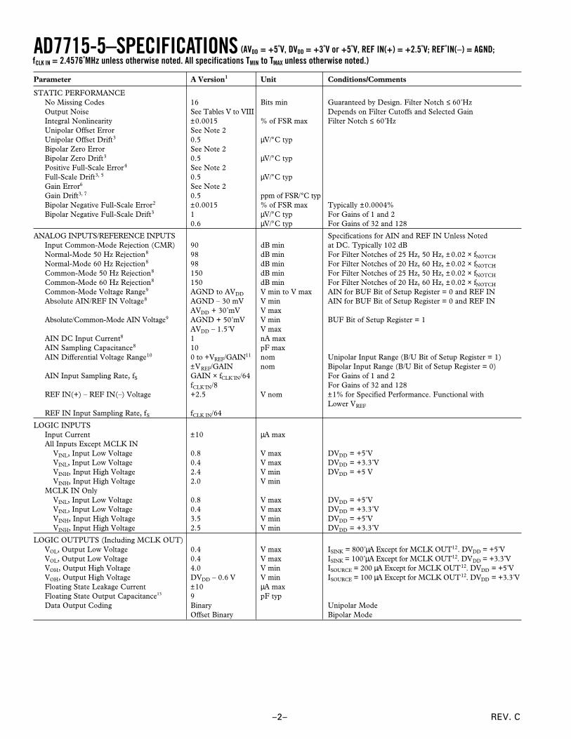
Parameter A Version1 Unit Conditions/Comments
STATIC PERFORMANCENo Missing Codes 16 Bits min Guaranteed by Design. Filter Notch ≤ 60 HzOutput Noise See Tables V to VIII Depends on Filter Cutoffs and Selected GainIntegral Nonlinearity ±0.0015 % of FSR max Filter Notch ≤ 60 HzUnipolar Offset Error See Note 2Unipolar Offset Drift3 0.5 µV/°C typBipolar Zero Error See Note 2Bipolar Zero Drift3 0.5 µV/°C typPositive Full-Scale Error4 See Note 2Full-Scale Drift3, 5 0.5 µV/°C typGain Error6 See Note 2Gain Drift3, 7 0.5 ppm of FSR/°C typBipolar Negative Full-Scale Error2 ±0.0015 % of FSR max Typically ±0.0004%Bipolar Negative Full-Scale Drift3 1 µV/°C typ For Gains of 1 and 2
0.6 µV/°C typ For Gains of 32 and 128
ANALOG INPUTS/REFERENCE INPUTS Specifications for AIN and REF IN Unless NotedInput Common-Mode Rejection (CMR) 90 dB min at DC. Typically 102 dBNormal-Mode 50 Hz Rejection8 98 dB min For Filter Notches of 25 Hz, 50 Hz, ± 0.02 × fNOTCH
Normal-Mode 60 Hz Rejection8 98 dB min For Filter Notches of 20 Hz, 60 Hz, ± 0.02 × fNOTCH
Common-Mode 50 Hz Rejection8 150 dB min For Filter Notches of 25 Hz, 50 Hz, ± 0.02 × fNOTCH
Common-Mode 60 Hz Rejection8 150 dB min For Filter Notches of 20 Hz, 60 Hz, ± 0.02 × fNOTCH
Common-Mode Voltage Range9 AGND to AVDD V min to V max AIN for BUF Bit of Setup Register = 0 and REF INAbsolute AIN/REF IN Voltage8 AGND – 30 mV V min AIN for BUF Bit of Setup Register = 0 and REF IN
AVDD + 30 mV V maxAbsolute/Common-Mode AIN Voltage9 AGND + 50 mV V min BUF Bit of Setup Register = 1
AVDD – 1.5 V V maxAIN DC Input Current8 1 nA maxAIN Sampling Capacitance8 10 pF maxAIN Differential Voltage Range10 0 to +VREF/GAIN11 nom Unipolar Input Range (B/U Bit of Setup Register = 1)
±VREF/GAIN nom Bipolar Input Range (B/U Bit of Setup Register = 0)AIN Input Sampling Rate, fS GAIN × fCLK IN/64 For Gains of 1 and 2
fCLK IN/8 For Gains of 32 and 128REF IN(+) – REF IN(–) Voltage +2.5 V nom ±1% for Specified Performance. Functional with
Lower VREF
REF IN Input Sampling Rate, fS fCLK IN/64
LOGIC INPUTSInput Current ±10 µA maxAll Inputs Except MCLK IN
VINL, Input Low Voltage 0.8 V max DVDD = +5 VVINL, Input Low Voltage 0.4 V max DVDD = +3.3 VVINH, Input High Voltage 2.4 V min DVDD = +5 VVINH, Input High Voltage 2.0 V min
MCLK IN OnlyVINL, Input Low Voltage 0.8 V max DVDD = +5 VVINL, Input Low Voltage 0.4 V max DVDD = +3.3 VVINH, Input High Voltage 3.5 V min DVDD = +5 VVINH, Input High Voltage 2.5 V min DVDD = +3.3 V
LOGIC OUTPUTS (Including MCLK OUT)VOL, Output Low Voltage 0.4 V max ISINK = 800 µA Except for MCLK OUT12. DVDD = +5 VVOL, Output Low Voltage 0.4 V max ISINK = 100 µA Except for MCLK OUT12. DVDD = +3.3 VVOH, Output High Voltage 4.0 V min ISOURCE = 200 µA Except for MCLK OUT12. DVDD = +5 VVOH, Output High Voltage DVDD – 0.6 V V min ISOURCE = 100 µA Except for MCLK OUT12. DVDD = +3.3 VFloating State Leakage Current ±10 µA maxFloating State Output Capacitance13 9 pF typData Output Coding Binary Unipolar Mode
Offset Binary Bipolar Mode
AD7715-5–SPECIFICATIONS (AVDD = +5 V, DVDD = +3 V or +5 V, REF IN(+) = +2.5 V; REF IN(–) = AGND;fCLK IN = 2.4576 MHz unless otherwise noted. All specifications TMIN to TMAX unless otherwise noted.)
REV. C–2–
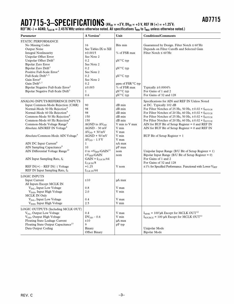
Parameter A Version1 Unit Conditions/Comments
STATIC PERFORMANCENo Missing Codes 16 Bits min Guaranteed by Design. Filter Notch ≤ 60 HzOutput Noise See Tables IX to XII Depends on Filter Cutoffs and Selected GainIntegral Nonlinearity ±0.0015 % of FSR max Filter Notch ≤ 60 HzUnipolar Offset Error See Note 2Unipolar Offset Drift3 0.2 µV/°C typBipolar Zero Error See Note 2Bipolar Zero Drift3 0.2 µV/°C typPositive Full-Scale Error4 See Note 2Full-Scale Drift3, 5 0.2 µV/°C typGain Error6 See Note 2Gain Drift3, 7 0.2 ppm of FSR/°C typBipolar Negative Full-Scale Error2 ±0.003 % of FSR max Typically ±0.0004%Bipolar Negative Full-Scale Drift3 1 µV/°C typ For Gains of 1 and 2
0.6 µV/°C typ For Gains of 32 and 128
ANALOG INPUTS/REFERENCE INPUTS Specifications for AIN and REF IN Unless NotedInput Common-Mode Rejection (CMR) 90 dB min at DC. Typically 102 dBNormal-Mode 50 Hz Rejection8 98 dB min For Filter Notches of 25 Hz, 50 Hz, ± 0.02 × fNOTCH
Normal-Mode 60 Hz Rejection8 98 dB min For Filter Notches of 20 Hz, 60 Hz, ± 0.02 × fNOTCH
Common-Mode 50 Hz Rejection8 150 dB min For Filter Notches of 25 Hz, 50 Hz, ± 0.02 × fNOTCH
Common-Mode 60 Hz Rejection8 150 dB min For Filter Notches of 20 Hz, 60 Hz, ± 0.02 × fNOTCH
Common-Mode Voltage Range9 AGND to AVDD V min to V max AIN for BUF Bit of Setup Register = 0 and REF INAbsolute AIN/REF IN Voltage8 AGND – 30 mV V min AIN for BUF Bit of Setup Register = 0 and REF IN
AVDD + 30 mV V maxAbsolute/Common-Mode AIN Voltage9 AGND + 50 mV V min BUF Bit of Setup Register = 1
AVDD – 1.5 V V maxAIN DC Input Current8 1 nA maxAIN Sampling Capacitance8 10 pF maxAIN Differential Voltage Range10 0 to +VREF/GAIN11 nom Unipolar Input Range (B/U Bit of Setup Register = 1)
±VREF/GAIN nom Bipolar Input Range (B/U Bit of Setup Register = 0)AIN Input Sampling Rate, fS GAIN × fCLK IN/64 For Gains of 1 and 2
fCLK IN/8 For Gains of 32 and 128REF IN(+) – REF IN(–) Voltage +1.25 V nom ±1% for Specified Performance. Functional with Lower VREF
REF IN Input Sampling Rate, fS fCLK IN/64
LOGIC INPUTSInput Current ±10 µA maxAll Inputs Except MCLK IN
VINL, Input Low Voltage 0.8 V maxVINH, Input High Voltage 2.0 V min
MCLK IN OnlyVINL, Input Low Voltage 0.4 V maxVINH, Input High Voltage 2.5 V min
LOGIC OUTPUTS (Including MCLK OUT)VOL, Output Low Voltage 0.4 V max ISINK = 100 µA Except for MCLK OUT12
VOH, Output High Voltage DVDD – 0.6 V min ISOURCE = 100 µA Except for MCLK OUT12
Floating State Leakage Current ±10 µA maxFloating State Output Capacitance13 9 pF typData Output Coding Binary Unipolar Mode
Offset Binary Bipolar Mode
AD7715AD7715-3–SPECIFICATIONS (AVDD = +3 V, DVDD = +3 V, REF IN (+) = +1.25 V;REF IN(–) = AGND; fCLK IN = 2.4576 MHz unless otherwise noted. All specifications TMIN to TMAX unless otherwise noted.)
–3–REV. C
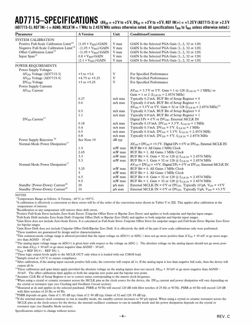
Parameter A Version Unit Conditions/Comments
SYSTEM CALIBRATIONPositive Full-Scale Calibration Limit14 (1.05 × VREF)/GAIN V max GAIN Is the Selected PGA Gain (1, 2, 32 or 128)Negative Full-Scale Calibration Limit14 –(1.05 × VREF)/GAIN V max GAIN Is the Selected PGA Gain (1, 2, 32 or 128)Offset Calibration Limit15 –(1.05 × VREF)/GAIN V max GAIN Is the Selected PGA Gain (1, 2, 32 or 128)Input Span15 0.8 × VREF/GAIN V min GAIN Is the Selected PGA Gain (1, 2, 32 or 128)
(2.1 × VREF)/GAIN V max GAIN Is the Selected PGA Gain (1, 2, 32 or 128)
POWER REQUIREMENTSPower Supply Voltages
AVDD Voltage (AD7715-3) +3 to +3.6 V For Specified PerformanceAVDD Voltage (AD7715-5) +4.75 to +5.25 V For Specified PerformanceDVDD Voltage +3 to +5.25 V For Specified Performance
Power Supply CurrentsAVDD Current AVDD = 3.3 V or 5 V. Gain = 1 to 128 (fCLK IN = 1 MHz) or
Gain = 1 or 2 (fCLK IN = 2.4576 MHz)0.27 mA max Typically 0.2 mA. BUF Bit of Setup Register = 00.6 mA max Typically 0.4 mA. BUF Bit of Setup Register = 1
AVDD = 3.3 V or 5 V. Gain = 32 or 128 (fCLK IN = 2.4576 MHz)16
0.5 mA max Typically 0.3 mA. BUF Bit of Setup Register = 01.1 mA max Typically 0.8 mA. BUF Bit of Setup Register = 1
DVDD Current17 Digital I/Ps = 0 V or DVDD. External MCLK IN0.18 mA max Typically 0.15 mA. DVDD = 3.3 V. fCLK IN = 1 MHz0.4 mA max Typically 0.3 mA. DVDD = 5 V. fCLK IN = 1 MHz0.5 mA max Typically 0.4 mA. DVDD = 3.3 V. fCLK IN = 2.4576 MHz0.8 mA max Typically 0.6 mA. DVDD = 5 V. fCLK IN = 2.4576 MHz
Power Supply Rejection 18 See Note 19 dB typNormal-Mode Power Dissipation17 AVDD = DVDD = +3.3 V. Digital I/Ps = 0 V or DVDD. External MCLK IN
1.5 mW max BUF Bit = 0. All Gains 1 MHz Clock2.65 mW max BUF Bit = 1. All Gains 1 MHz Clock3.3 mW max BUF Bit = 0. Gain = 32 or 128 @ fCLK IN = 2.4576 MHz5.3 mW max BUF Bit = 1. Gain = 32 or 128 @ fCLK IN = 2.4576 MHz
Normal-Mode Power Dissipation17 AVDD = DVDD = +5 V. Digital I/Ps = 0 V or DVDD. External MCLK IN3.25 mW max BUF Bit = 0. All Gains 1 MHz Clock5 mW max BUF Bit = 1. All Gains 1 MHz Clock6.5 mW max BUF Bit = 0. Gain = 32 or 128 @ fCLK IN = 2.4576 MHz9.5 mW max BUF Bit = 1. Gain = 32 or 128 @ fCLK IN = 2.4576 MHz
Standby (Power-Down) Current20 20 µA max External MCLK IN = 0 V or DVDD. Typically 10 µA. VDD = +5 VStandby (Power-Down) Current20 10 µA max External MCLK IN = 0 V or DVDD. Typically 5 µA. VDD = +3.3 V
NOTES1Temperature Range as follows: A Version, –40°C to +85°C.2A calibration is effectively a conversion so these errors will be of the order of the conversion noise shown in Tables V to XII. This applies after calibration at thetemperature of interest.
3Recalibration at any temperature will remove these drift errors.4Positive Full-Scale Error includes Zero-Scale Errors (Unipolar Offset Error or Bipolar Zero Error) and applies to both unipolar and bipolar input ranges.5Full-Scale Drift includes Zero-Scale Drift (Unipolar Offset Drift or Bipolar Zero Drift) and applies to both unipolar and bipolar input ranges.6Gain Error does not include Zero-Scale Errors. It is calculated as Full-Scale Error–Unipolar Offset Error for unipolar ranges and Full-Scale Error–Bipolar Zero Errorfor bipolar ranges.
7Gain Error Drift does not include Unipolar Offset Drift/Bipolar Zero Drift. It is effectively the drift of the part if zero scale calibrations only were performed.8These numbers are guaranteed by design and/or characterization.9This common-mode voltage range is allowed provided that the input voltage on AIN(+) or AIN(–) does not go more positive than A VDD + 30 mV or go more nega-tive than AGND – 30 mV.
10The analog input voltage range on AIN(+) is given here with respect to the voltage on AIN(–). The absolute voltage on the analog inputs should not go more posi-tive than AVDD + 30 mV or go more negative than AGND – 30 mV.
11VREF = REF IN(+) – REF IN(–).12These logic output levels apply to the MCLK OUT only when it is loaded with one CMOS load.13Sample tested at +25°C to ensure compliance.14After calibration, if the analog input exceeds positive full scale, the converter will output all 1s. If the analog input is less than negative full scale, then the device will
output all 0s.15These calibration and span limits apply provided the absolute voltage on the analog inputs does not exceed AVDD + 30 mV or go more negative than AGND –
30 mV. The offset calibration limit applies to both the unipolar zero point and the bipolar zero point.16Assumes CLK Bit of Setup Register is set to correct status corresponding to the master clock frequency.17When using a crystal or ceramic resonator across the MCLK pins as the clock source for the device, the DVDD current and power dissipation will vary depending on
the crystal or resonator type (see Clocking and Oscillator Circuit section).18Measured at dc and applies in the selected passband. PSRR at 50 Hz will exceed 120 dB with filter notches of 25 Hz or 50 Hz. PSRR at 60 Hz will exceed 120 dB
with filter notches of 20 Hz or 60 Hz.19PSRR depends on gain. Gain of 1: 85 dB typ; Gain of 2: 90 dB typ; Gains of 32 and 128: 95 dB typ.20If the external master clock continues to run in standby mode, the standby current increases to 50 µA typical. When using a crystal or ceramic resonator across the
MCLK pins as the clock source for the device, the internal oscillator continues to run in standby mode and the power dissipation depends on the crystal orresonator type (see Standby Mode section).
Specifications subject to change without notice.
AD7715–SPECIFICATIONS A (AVDD = +3 V to +5 V, DVDD = +3 V to +5 V, REF IN(+) = +1.25 V (AD7715-3) or +2.5 V(AD7715-5); REF IN(–) = AGND; MCLK IN = 1 MHz to 2.4576 MHz unless otherwise noted. All specifications TMIN to TMAX unless otherwise noted.)
–4– REV. C

AD7715
–5–REV. C
TIMING CHARACTERISTICS1, 2
Limit at TMIN, TMAX
Parameter (A Version) Unit Conditions/Comments
fCLKIN3, 4 400 kHz min Master Clock Frequency: Crystal Oscillator or Externally Supplied
2.5 MHz max for Specified PerformancetCLK IN LO 0.4 × tCLK IN ns min Master Clock Input Low Time. tCLK IN = 1/fCLK IN
tCLK IN HI 0.4 × tCLK IN ns min Master Clock Input High Timet1 500 × tCLK IN ns nom DRDY High Timet2 100 ns min RESET PulsewidthRead Operation
t3 0 ns min DRDY to CS Setup Timet4 120 ns min CS Falling Edge to SCLK Rising Edge Setup Timet5
5 0 ns min SCLK Falling Edge to Data Valid Delay80 ns max DVDD = +5 V100 ns max DVDD = +3.3 V
t6 100 ns min SCLK High Pulsewidtht7 100 ns min SCLK Low Pulsewidtht8 0 ns min CS Rising Edge to SCLK Rising Edge Hold Timet9
6 10 ns min Bus Relinquish Time after SCLK Rising Edge60 ns max DVDD = +5 V100 ns max DVDD = +3.3 V
t10 100 ns max SCLK Falling Edge to DRDY High7
Write Operationt11 120 ns min CS Falling Edge to SCLK Rising Edge Setup Timet12 30 ns min Data Valid to SCLK Rising Edge Setup Timet13 20 ns min Data Valid to SCLK Rising Edge Hold Timet14 100 ns min SCLK High Pulsewidtht15 100 ns min SCLK Low Pulsewidtht16 0 ns min CS Rising Edge to SCLK Rising Edge Hold Time
NOTES1Sample tested at +25°C to ensure compliance. All input signals are specified with tr = tf = 5 ns (10% to 90% of D VDD) and timed from a voltage level of 1.6 V.2See Figures 6 and 7.3CLKIN Duty Cycle range is 45% to 55%. CLKIN must be supplied whenever the AD7715 is not in Standby mode. If no clock is present in this case, thedevice can draw higher current than specified and possibly become uncalibrated.
4The AD7715 is production tested with fCLKIN at 2.4576 MHz (1 MHz for some IDD tests). It is guaranteed by characterization to operate at 400 kHz.5These numbers are measured with the load circuit of Figure 1 and defined as the time required for the output to cross the VOL or VOH limits.6These numbers are derived from the measured time taken by the data output to change 0.5 V when loaded with the circuit of Figure 1. The measured number isthen extrapolated back to remove effects of charging or discharging the 50 pF capacitor. This means that the times quoted in the timing characteristics are thetrue bus relinquish times of the part and as such are independent of external bus loading capacitances.
7DRDY returns high after the first read from the device after an output update. The same data can be read again, if required, while DRDY is high although careshould be taken that subsequent reads do not occur close to the next output update.
Specifications subject to change without notice.
TOOUTPUT
PIN+1.6V
ISINK (800mA AT DVDD = 5V 100mA AT DVDD = 3.3V)
50pF
ISOURCE (200mA AT DVDD = 5V 100mA AT DVDD = 3.3V)
Figure 1. Load Circuit for Access Time and Bus Relinquish Time
(DVDD = +3 V to +5.25 V; AVDD = +3 V to +5.25 V; AGND = DGND = 0 V; fCLKIN = 2.4576 MHz;Input Logic 0 = 0 V, Logic 1 = DVDD, unless otherwise noted)
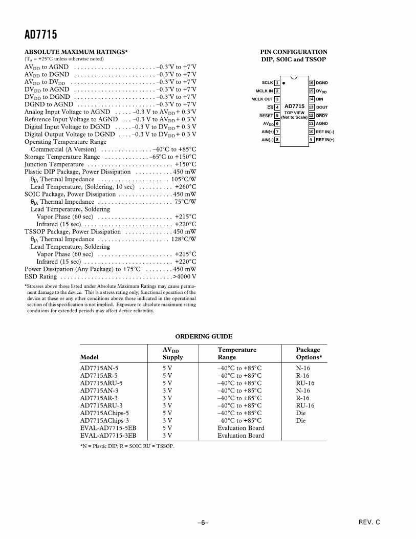
REV. C
AD7715
–6–
ORDERING GUIDE
AVDD Temperature PackageModel Supply Range Options*
AD7715AN-5 5 V –40°C to +85°C N-16AD7715AR-5 5 V –40°C to +85°C R-16AD7715ARU-5 5 V –40°C to +85°C RU-16AD7715AN-3 3 V –40°C to +85°C N-16AD7715AR-3 3 V –40°C to +85°C R-16AD7715ARU-3 3 V –40°C to +85°C RU-16AD7715AChips-5 5 V –40°C to +85°C DieAD7715AChips-3 3 V –40°C to +85°C DieEVAL-AD7715-5EB 5 V Evaluation BoardEVAL-AD7715-3EB 3 V Evaluation Board
*N = Plastic DIP; R = SOIC RU = TSSOP.
ABSOLUTE MAXIMUM RATINGS*(TA = +25°C unless otherwise noted)
AVDD to AGND . . . . . . . . . . . . . . . . . . . . . . . . –0.3 V to +7 VAVDD to DGND . . . . . . . . . . . . . . . . . . . . . . . . –0.3 V to +7 VAVDD to DVDD . . . . . . . . . . . . . . . . . . . . . . . . . –0.3 V to +7 VDVDD to AGND . . . . . . . . . . . . . . . . . . . . . . . . –0.3 V to +7 VDVDD to DGND . . . . . . . . . . . . . . . . . . . . . . . . –0.3 V to +7 VDGND to AGND . . . . . . . . . . . . . . . . . . . . . . . –0.3 V to +7 VAnalog Input Voltage to AGND . . . . . –0.3 V to AVDD + 0.3 VReference Input Voltage to AGND . . . –0.3 V to AVDD + 0.3 VDigital Input Voltage to DGND . . . . . –0.3 V to DVDD + 0.3 VDigital Output Voltage to DGND . . . . –0.3 V to DVDD + 0.3 VOperating Temperature Range
Commercial (A Version) . . . . . . . . . . . . . . . –40°C to +85°CStorage Temperature Range . . . . . . . . . . . . . –65°C to +150°CJunction Temperature . . . . . . . . . . . . . . . . . . . . . . . . . +150°CPlastic DIP Package, Power Dissipation . . . . . . . . . . . 450 mW
θJA Thermal Impedance . . . . . . . . . . . . . . . . . . . . . 105°C/WLead Temperature, (Soldering, 10 sec) . . . . . . . . . . +260°C
SOIC Package, Power Dissipation . . . . . . . . . . . . . . . . 450 mWθJA Thermal Impedance . . . . . . . . . . . . . . . . . . . . . . 75°C/WLead Temperature, Soldering
Vapor Phase (60 sec) . . . . . . . . . . . . . . . . . . . . . . +215°CInfrared (15 sec) . . . . . . . . . . . . . . . . . . . . . . . . . . +220°C
TSSOP Package, Power Dissipation . . . . . . . . . . . . . . 450 mWθJA Thermal Impedance . . . . . . . . . . . . . . . . . . . . . 128°C/WLead Temperature, Soldering
Vapor Phase (60 sec) . . . . . . . . . . . . . . . . . . . . . . +215°CInfrared (15 sec) . . . . . . . . . . . . . . . . . . . . . . . . . . +220°C
Power Dissipation (Any Package) to +75°C . . . . . . . . 450 mWESD Rating . . . . . . . . . . . . . . . . . . . . . . . . . . . . . . . . .>4000 V*Stresses above those listed under Absolute Maximum Ratings may cause perma-
nent damage to the device. This is a stress rating only; functional operation of thedevice at these or any other conditions above those indicated in the operationalsection of this specification is not implied. Exposure to absolute maximum ratingconditions for extended periods may affect device reliability.
PIN CONFIGURATIONDIP, SOIC and TSSOP
14
13
12
11
16
15
10
98
1
2
3
4
7
6
5TOP VIEW
(Not to Scale)
AD7715
SCLK
DOUT
DIN
DVDD
DGND
MCLK IN
MCLK OUT
CS
REF IN(+)
AGND
DRDYRESET
AVDD
AIN(+)
AIN(–)
REF IN(–)
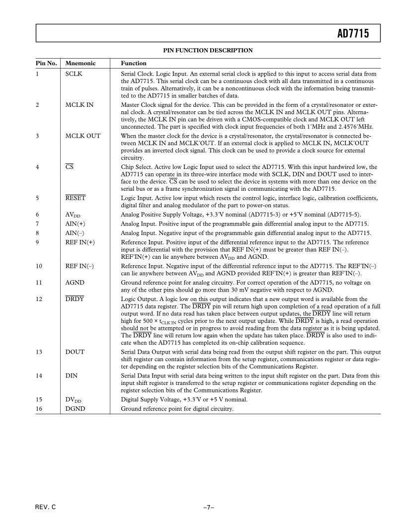
AD7715
–7–REV. C
PIN FUNCTION DESCRIPTION
Pin No. Mnemonic Function
1 SCLK Serial Clock. Logic Input. An external serial clock is applied to this input to access serial data fromthe AD7715. This serial clock can be a continuous clock with all data transmitted in a continuoustrain of pulses. Alternatively, it can be a noncontinuous clock with the information being transmit-ted to the AD7715 in smaller batches of data.
2 MCLK IN Master Clock signal for the device. This can be provided in the form of a crystal/resonator or exter-nal clock. A crystal/resonator can be tied across the MCLK IN and MCLK OUT pins. Alterna-tively, the MCLK IN pin can be driven with a CMOS-compatible clock and MCLK OUT leftunconnected. The part is specified with clock input frequencies of both 1 MHz and 2.4576 MHz.
3 MCLK OUT When the master clock for the device is a crystal/resonator, the crystal/resonator is connected be-tween MCLK IN and MCLK OUT. If an external clock is applied to MCLK IN, MCLK OUTprovides an inverted clock signal. This clock can be used to provide a clock source for externalcircuitry.
4 CS Chip Select. Active low Logic Input used to select the AD7715. With this input hardwired low, theAD7715 can operate in its three-wire interface mode with SCLK, DIN and DOUT used to inter-face to the device. CS can be used to select the device in systems with more than one device on theserial bus or as a frame synchronization signal in communicating with the AD7715.
5 RESET Logic Input. Active low input which resets the control logic, interface logic, calibration coefficients,digital filter and analog modulator of the part to power-on status.
6 AVDD Analog Positive Supply Voltage, +3.3 V nominal (AD7715-3) or +5 V nominal (AD7715-5).
7 AIN(+) Analog Input. Positive input of the programmable gain differential analog input to the AD7715.
8 AIN(–) Analog Input. Negative input of the programmable gain differential analog input to the AD7715.
9 REF IN(+) Reference Input. Positive input of the differential reference input to the AD7715. The referenceinput is differential with the provision that REF IN(+) must be greater than REF IN(–).REF IN(+) can lie anywhere between AVDD and AGND.
10 REF IN(–) Reference Input. Negative input of the differential reference input to the AD7715. The REF IN(–)can lie anywhere between AVDD and AGND provided REF IN(+) is greater than REF IN(–).
11 AGND Ground reference point for analog circuitry. For correct operation of the AD7715, no voltage onany of the other pins should go more than 30 mV negative with respect to AGND.
12 DRDY Logic Output. A logic low on this output indicates that a new output word is available from theAD7715 data register. The DRDY pin will return high upon completion of a read operation of a fulloutput word. If no data read has taken place between output updates, the DRDY line will returnhigh for 500 × tCLK IN cycles prior to the next output update. While DRDY is high, a read operationshould not be attempted or in progress to avoid reading from the data register as it is being updated.The DRDY line will return low again when the update has taken place. DRDY is also used to indi-cate when the AD7715 has completed its on-chip calibration sequence.
13 DOUT Serial Data Output with serial data being read from the output shift register on the part. This outputshift register can contain information from the setup register, communications register or data regis-ter depending on the register selection bits of the Communications Register.
14 DIN Serial Data Input with serial data being written to the input shift register on the part. Data from thisinput shift register is transferred to the setup register or communications register depending on theregister selection bits of the Communications Register.
15 DVDD Digital Supply Voltage, +3.3 V or +5 V nominal.
16 DGND Ground reference point for digital circuitry.
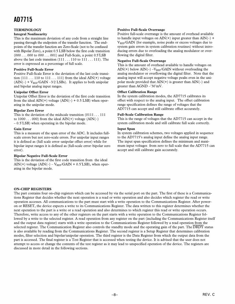
REV. C
AD7715
–8–
TERMINOLOGYIntegral NonlinearityThis is the maximum deviation of any code from a straight linepassing through the endpoints of the transfer function. The end-points of the transfer function are Zero-Scale (not to be confusedwith Bipolar Zero), a point 0.5 LSB below the first code transition(000 . . . 000 to 000 . . . 001) and Full-Scale, a point 0.5 LSBabove the last code transition (111 . . . 110 to 111 . . . 111). Theerror is expressed as a percentage of full scale.
Positive Full-Scale ErrorPositive Full-Scale Error is the deviation of the last code transi-tion (111 . . . 110 to 111 . . . 111) from the ideal AIN(+) voltage(AIN(–) + VREF/GAIN –3/2 LSBs). It applies to both unipolarand bipolar analog input ranges.
Unipolar Offset ErrorUnipolar Offset Error is the deviation of the first code transitionfrom the ideal AIN(+) voltage (AIN(–) + 0.5 LSB) when oper-ating in the unipolar mode.
Bipolar Zero ErrorThis is the deviation of the midscale transition (0111 . . . 111to 1000 . . . 000) from the ideal AIN(+) voltage (AIN(–)– 0.5 LSB) when operating in the bipolar mode.
Gain ErrorThis is a measure of the span error of the ADC. It includes full-scale errors but not zero-scale errors. For unipolar input rangesit is defined as (full scale error–unipolar offset error) while forbipolar input ranges it is defined as (full-scale error–bipolar zeroerror).
Bipolar Negative Full-Scale ErrorThis is the deviation of the first code transition from the idealAIN(+) voltage (AIN(–) – VREF/GAIN + 0.5 LSB), when oper-ating in the bipolar mode.
Positive Full-Scale OverrangePositive full-scale overrange is the amount of overhead availableto handle input voltages on AIN(+) input greater than AIN(–) +VREF/GAIN (for example, noise peaks or excess voltages due tosystem gain errors in system calibration routines) without intro-ducing errors due to overloading the analog modulator or over-flowing the digital filter.
Negative Full-Scale OverrangeThis is the amount of overhead available to handle voltages onAIN(+) below AIN(–) –VREF/GAIN without overloading theanalog modulator or overflowing the digital filter. Note that theanalog input will accept negative voltage peaks even in the uni-polar mode provided that AIN(+) is greater than AIN(–) andgreater than AGND – 30 mV.
Offset Calibration RangeIn the system calibration modes, the AD7715 calibrates itsoffset with respect to the analog input. The offset calibrationrange specification defines the range of voltages that theAD7715 can accept and still calibrate offset accurately.
Full-Scale Calibration RangeThis is the range of voltages that the AD7715 can accept in thesystem calibration mode and still calibrate full scale correctly.
Input SpanIn system calibration schemes, two voltages applied in sequenceto the AD7715’s analog input define the analog input range.The input span specification defines the minimum and maxi-mum input voltages from zero to full scale that the AD7715 canaccept and still calibrate gain accurately.
ON-CHIP REGISTERSThe part contains four on-chip registers which can be accessed by via the serial port on the part. The first of these is a Communica-tions Register that decides whether the next operation is a read or write operation and also decides which register the read or writeoperation accesses. All communications to the part must start with a write operation to the Communications Register. After power-on or RESET, the device expects a write to its Communications Register. The data written to this register determines whether thenext operation to the part is a write or a read operation and also determines to which register this read or write operation occurs.Therefore, write access to any of the other registers on the part starts with a write operation to the Communications Register fol-lowed by a write to the selected register. A read operation from any register on the part (including the Communications Register itselfand the output data register) starts with a write operation to the Communications Register followed by a read operation from theselected register. The Communication Register also controls the standby mode and the operating gain of the part. The DRDY statusis also available by reading from the Communications Register. The second register is a Setup Register that determines calibrationmodes, filter selection and bipolar/unipolar operation. The third register is the Data Register from which the output data from thepart is accessed. The final register is a Test Register that is accessed when testing the device. It is advised that the user does notattempt to access or change the contents of the test register as it may lead to unspecified operation of the device. The registers arediscussed in more detail in the following sections.
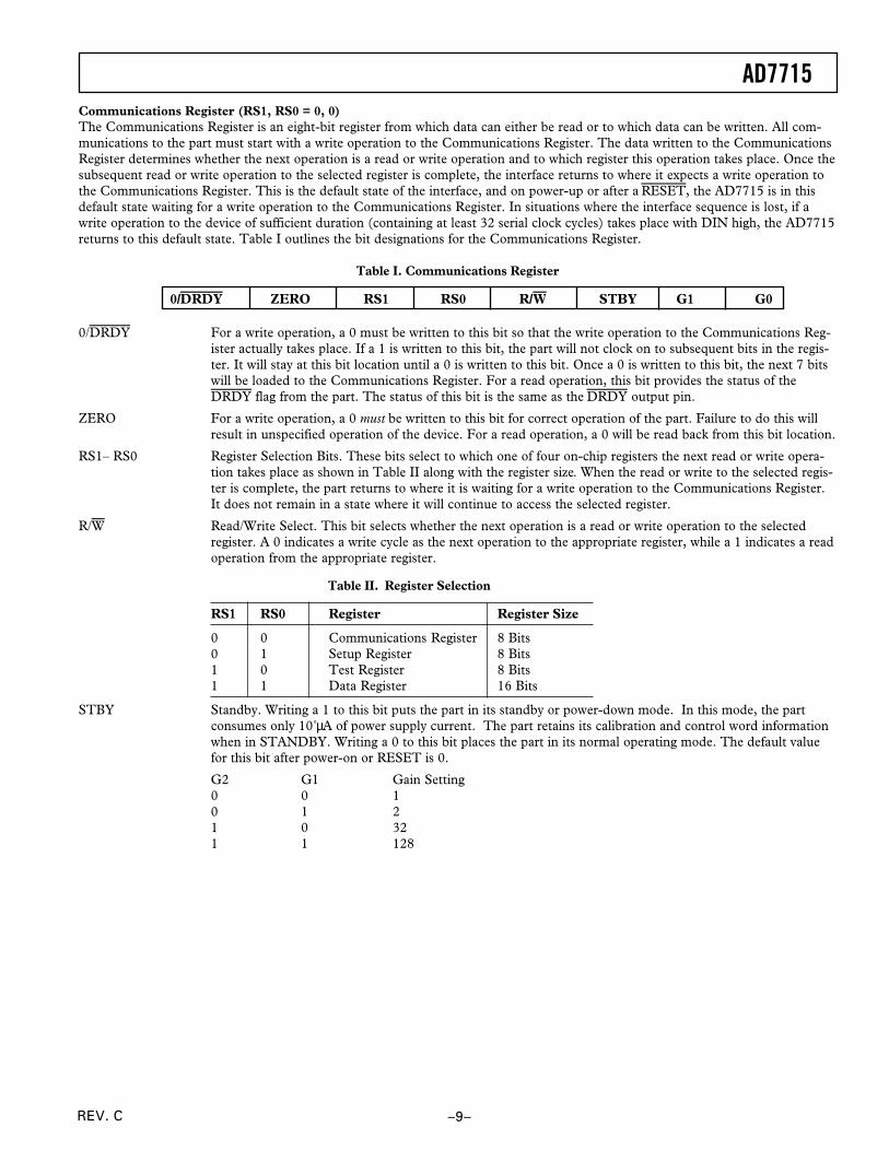
AD7715
–9–REV. C
Communications Register (RS1, RS0 = 0, 0)The Communications Register is an eight-bit register from which data can either be read or to which data can be written. All com-munications to the part must start with a write operation to the Communications Register. The data written to the CommunicationsRegister determines whether the next operation is a read or write operation and to which register this operation takes place. Once thesubsequent read or write operation to the selected register is complete, the interface returns to where it expects a write operation tothe Communications Register. This is the default state of the interface, and on power-up or after a RESET, the AD7715 is in thisdefault state waiting for a write operation to the Communications Register. In situations where the interface sequence is lost, if awrite operation to the device of sufficient duration (containing at least 32 serial clock cycles) takes place with DIN high, the AD7715returns to this default state. Table I outlines the bit designations for the Communications Register.
Table I. Communications Register
0/DRDY ZERO RS1 RS0 R/W STBY G1 G0
0/DRDY For a write operation, a 0 must be written to this bit so that the write operation to the Communications Reg-ister actually takes place. If a 1 is written to this bit, the part will not clock on to subsequent bits in the regis-ter. It will stay at this bit location until a 0 is written to this bit. Once a 0 is written to this bit, the next 7 bitswill be loaded to the Communications Register. For a read operation, this bit provides the status of theDRDY flag from the part. The status of this bit is the same as the DRDY output pin.
ZERO For a write operation, a 0 must be written to this bit for correct operation of the part. Failure to do this willresult in unspecified operation of the device. For a read operation, a 0 will be read back from this bit location.
RS1– RS0 Register Selection Bits. These bits select to which one of four on-chip registers the next read or write opera-tion takes place as shown in Table II along with the register size. When the read or write to the selected regis-ter is complete, the part returns to where it is waiting for a write operation to the Communications Register.It does not remain in a state where it will continue to access the selected register.
R/W Read/Write Select. This bit selects whether the next operation is a read or write operation to the selectedregister. A 0 indicates a write cycle as the next operation to the appropriate register, while a 1 indicates a readoperation from the appropriate register.
Table II. Register Selection
RS1 RS0 Register Register Size
0 0 Communications Register 8 Bits0 1 Setup Register 8 Bits1 0 Test Register 8 Bits1 1 Data Register 16 Bits
STBY Standby. Writing a 1 to this bit puts the part in its standby or power-down mode. In this mode, the partconsumes only 10 µA of power supply current. The part retains its calibration and control word informationwhen in STANDBY. Writing a 0 to this bit places the part in its normal operating mode. The default valuefor this bit after power-on or RESET is 0.
G2 G1 Gain Setting0 0 10 1 21 0 321 1 128
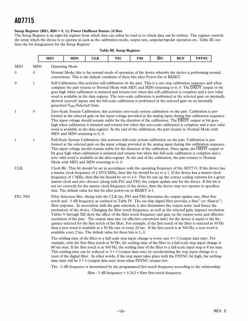
REV. C
AD7715
–10–
Setup Register (RS1, RS0 = 0, 1); Power On/Reset Status: 28 HexThe Setup Register is an eight-bit register from which data can either be read or to which data can be written. This register controlsthe setup which the device is to operate in such as the calibration mode, output rate, unipolar/bipolar operation etc. Table III out-lines the bit designations for the Setup Register.
Table III. Setup Register
MD1 MD0 CLK FS1 FS0 B/U BUF FSYNC
MD1 MD0 Operating Mode
0 0 Normal Mode; this is the normal mode of operation of the device whereby the device is performing normalconversions. This is the default condition of these bits after Power-On or RESET.
0 1 Self-Calibration; this activates self-calibration on the part. This is a one step calibration sequence and whencomplete the part returns to Normal Mode with MD1 and MD0 returning to 0, 0. The DRDY output or bitgoes high when calibration is initiated and returns low when this self-calibration is complete and a new validword is available in the data register. The zero-scale calibration is performed at the selected gain on internallyshorted (zeroed) inputs and the full-scale calibration is performed at the selected gain on an internallygenerated VREF/Selected Gain.
1 0 Zero-Scale System Calibration; this activates zero-scale system calibration on the part. Calibration is per-formed at the selected gain on the input voltage provided at the analog input during this calibration sequence.This input voltage should remain stable for the duration of the calibration. The DRDY output or bit goeshigh when calibration is initiated and returns low when this zero-scale calibration is complete and a new validword is available in the data register. At the end of the calibration, the part returns to Normal Mode withMD1 and MD0 returning to 0, 0.
1 1 Full-Scale System Calibration; this activates full-scale system calibration on the part. Calibration is per-formed at the selected gain on the input voltage provided at the analog input during this calibration sequence.This input voltage should remain stable for the duration of the calibration. Once again, the DRDY output orbit goes high when calibration is initiated and returns low when this full-scale calibration is complete and anew valid word is available in the data register. At the end of the calibration, the part returns to NormalMode with MD1 and MD0 returning to 0, 0.
CLK Clock Bit. This bit should be set in accordance with the operating frequency of the AD7715. If the device hasa master clock frequency of 2.4576 MHz, then this bit should be set to a 1. If the device has a master clockfrequency of 1 MHz, then this bit should be set to a 0. This bit sets up the correct scaling currents for a givenmaster clock and also chooses (along with FS1 and FS0) the output update rate for the device. If this bit isnot set correctly for the master clock frequency of the device, then the device may not operate to specifica-tion. The default value for this bit after power-on or RESET is 1.
FS1, FS0 Filter Selection Bits. Along with the CLK bit, FS1 and FS0 determine the output update rate, filter firstnotch and –3 dB frequency as outlined in Table IV. The on-chip digital filter provides a Sinc3 (or (Sinx/x)3 )filter response. In association with the gain selection, it also determines the output noise (and hence theresolution) of the device. Changing the filter notch frequency, as well as the selected gain, impacts resolution.Tables V through XII show the effect of the filter notch frequency and gain on the output noise and effectiveresolution of the part. The output data rate (or effective conversion time) for the device is equal to the fre-quency selected for the first notch of the filter. For example, if the first notch of the filter is selected at 50 Hzthen a new word is available at a 50 Hz rate or every 20 ms. If the first notch is at 500 Hz, a new word isavailable every 2 ms. The default value for these bits is 1, 0.
The settling-time of the filter to a full-scale step input change is worst case 4 × 1/(output data rate). Forexample, with the first filter notch at 50 Hz, the settling time of the filter to a full-scale step input change is80 ms max. If the first notch is at 500 Hz, the settling time of the filter to a full-scale input step is 8 ms max.This settling-time can be reduced to 3 × 1/(output data rate) by synchronizing the step input change to areset of the digital filter. In other words, if the step input takes place with the FSYNC bit high, the settling-time time will be 3 × 1/(output data rate) from when FSYNC returns low.
The –3 dB frequency is determined by the programmed first notch frequency according to the relationship:
filter –3 dB frequency = 0.262 × filter first notch frequency.
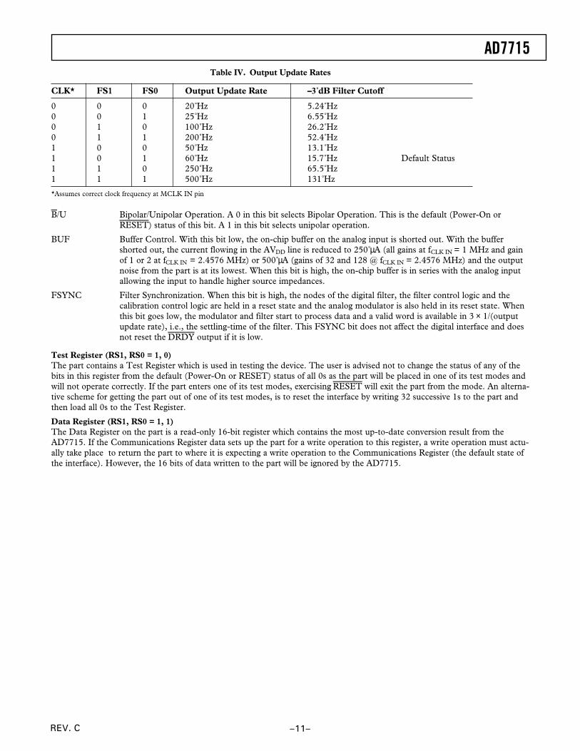
AD7715
–11–REV. C
Table IV. Output Update Rates
CLK* FS1 FS0 Output Update Rate –3 dB Filter Cutoff
0 0 0 20 Hz 5.24 Hz0 0 1 25 Hz 6.55 Hz0 1 0 100 Hz 26.2 Hz0 1 1 200 Hz 52.4 Hz1 0 0 50 Hz 13.1 Hz1 0 1 60 Hz 15.7 Hz Default Status1 1 0 250 Hz 65.5 Hz1 1 1 500 Hz 131 Hz
*Assumes correct clock frequency at MCLK IN pin
B/U Bipolar/Unipolar Operation. A 0 in this bit selects Bipolar Operation. This is the default (Power-On orRESET) status of this bit. A 1 in this bit selects unipolar operation.
BUF Buffer Control. With this bit low, the on-chip buffer on the analog input is shorted out. With the buffershorted out, the current flowing in the AVDD line is reduced to 250 µA (all gains at fCLK IN = 1 MHz and gainof 1 or 2 at fCLK IN = 2.4576 MHz) or 500 µA (gains of 32 and 128 @ fCLK IN = 2.4576 MHz) and the outputnoise from the part is at its lowest. When this bit is high, the on-chip buffer is in series with the analog inputallowing the input to handle higher source impedances.
FSYNC Filter Synchronization. When this bit is high, the nodes of the digital filter, the filter control logic and thecalibration control logic are held in a reset state and the analog modulator is also held in its reset state. Whenthis bit goes low, the modulator and filter start to process data and a valid word is available in 3 × 1/(outputupdate rate), i.e., the settling-time of the filter. This FSYNC bit does not affect the digital interface and doesnot reset the DRDY output if it is low.
Test Register (RS1, RS0 = 1, 0)The part contains a Test Register which is used in testing the device. The user is advised not to change the status of any of thebits in this register from the default (Power-On or RESET) status of all 0s as the part will be placed in one of its test modes andwill not operate correctly. If the part enters one of its test modes, exercising RESET will exit the part from the mode. An alterna-tive scheme for getting the part out of one of its test modes, is to reset the interface by writing 32 successive 1s to the part andthen load all 0s to the Test Register.
Data Register (RS1, RS0 = 1, 1)The Data Register on the part is a read-only 16-bit register which contains the most up-to-date conversion result from theAD7715. If the Communications Register data sets up the part for a write operation to this register, a write operation must actu-ally take place to return the part to where it is expecting a write operation to the Communications Register (the default state ofthe interface). However, the 16 bits of data written to the part will be ignored by the AD7715.
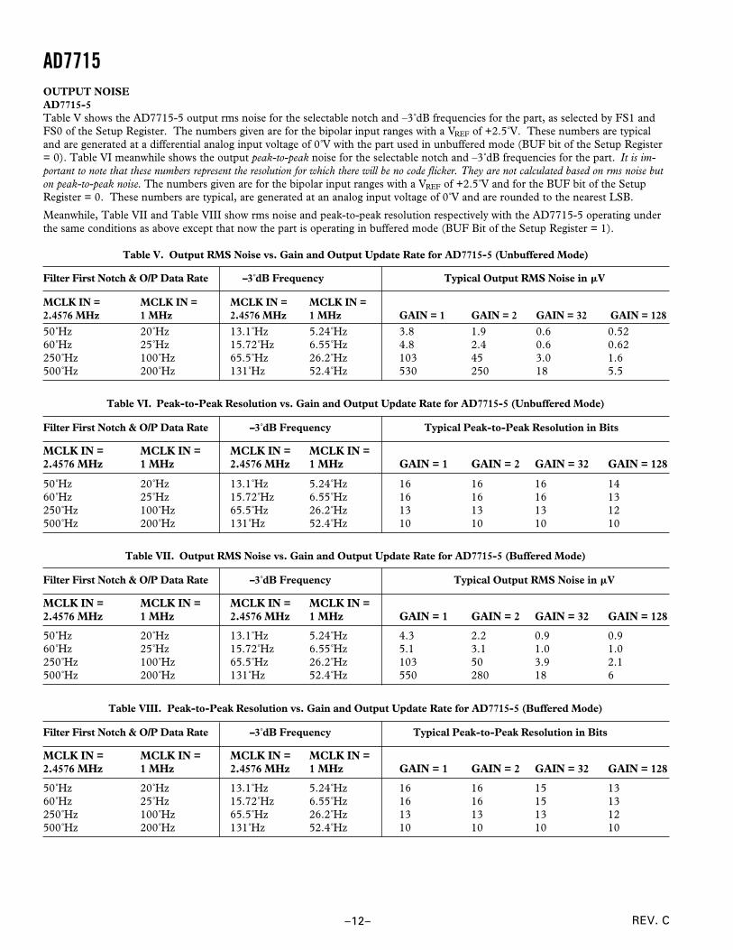
REV. C
AD7715
–12–
OUTPUT NOISEAD7715-5Table V shows the AD7715-5 output rms noise for the selectable notch and –3 dB frequencies for the part, as selected by FS1 andFS0 of the Setup Register. The numbers given are for the bipolar input ranges with a VREF of +2.5 V. These numbers are typicaland are generated at a differential analog input voltage of 0 V with the part used in unbuffered mode (BUF bit of the Setup Register= 0). Table VI meanwhile shows the output peak-to-peak noise for the selectable notch and –3 dB frequencies for the part. It is im-portant to note that these numbers represent the resolution for which there will be no code flicker. They are not calculated based on rms noise buton peak-to-peak noise. The numbers given are for the bipolar input ranges with a VREF of +2.5 V and for the BUF bit of the SetupRegister = 0. These numbers are typical, are generated at an analog input voltage of 0 V and are rounded to the nearest LSB.
Meanwhile, Table VII and Table VIII show rms noise and peak-to-peak resolution respectively with the AD7715-5 operating underthe same conditions as above except that now the part is operating in buffered mode (BUF Bit of the Setup Register = 1).
Table V. Output RMS Noise vs. Gain and Output Update Rate for AD7715-5 (Unbuffered Mode)
Filter First Notch & O/P Data Rate –3 dB Frequency Typical Output RMS Noise in mV
MCLK IN = MCLK IN = MCLK IN = MCLK IN =2.4576 MHz 1 MHz 2.4576 MHz 1 MHz GAIN = 1 GAIN = 2 GAIN = 32 GAIN = 128
50 Hz 20 Hz 13.1 Hz 5.24 Hz 3.8 1.9 0.6 0.5260 Hz 25 Hz 15.72 Hz 6.55 Hz 4.8 2.4 0.6 0.62250 Hz 100 Hz 65.5 Hz 26.2 Hz 103 45 3.0 1.6500 Hz 200 Hz 131 Hz 52.4 Hz 530 250 18 5.5
Table VI. Peak-to-Peak Resolution vs. Gain and Output Update Rate for AD7715-5 (Unbuffered Mode)
Filter First Notch & O/P Data Rate –3 dB Frequency Typical Peak-to-Peak Resolution in Bits
MCLK IN = MCLK IN = MCLK IN = MCLK IN =2.4576 MHz 1 MHz 2.4576 MHz 1 MHz GAIN = 1 GAIN = 2 GAIN = 32 GAIN = 128
50 Hz 20 Hz 13.1 Hz 5.24 Hz 16 16 16 1460 Hz 25 Hz 15.72 Hz 6.55 Hz 16 16 16 13250 Hz 100 Hz 65.5 Hz 26.2 Hz 13 13 13 12500 Hz 200 Hz 131 Hz 52.4 Hz 10 10 10 10
Table VII. Output RMS Noise vs. Gain and Output Update Rate for AD7715-5 (Buffered Mode)
Filter First Notch & O/P Data Rate –3 dB Frequency Typical Output RMS Noise in mV
MCLK IN = MCLK IN = MCLK IN = MCLK IN =2.4576 MHz 1 MHz 2.4576 MHz 1 MHz GAIN = 1 GAIN = 2 GAIN = 32 GAIN = 128
50 Hz 20 Hz 13.1 Hz 5.24 Hz 4.3 2.2 0.9 0.960 Hz 25 Hz 15.72 Hz 6.55 Hz 5.1 3.1 1.0 1.0250 Hz 100 Hz 65.5 Hz 26.2 Hz 103 50 3.9 2.1500 Hz 200 Hz 131 Hz 52.4 Hz 550 280 18 6
Table VIII. Peak-to-Peak Resolution vs. Gain and Output Update Rate for AD7715-5 (Buffered Mode)
Filter First Notch & O/P Data Rate –3 dB Frequency Typical Peak-to-Peak Resolution in Bits
MCLK IN = MCLK IN = MCLK IN = MCLK IN =2.4576 MHz 1 MHz 2.4576 MHz 1 MHz GAIN = 1 GAIN = 2 GAIN = 32 GAIN = 128
50 Hz 20 Hz 13.1 Hz 5.24 Hz 16 16 15 1360 Hz 25 Hz 15.72 Hz 6.55 Hz 16 16 15 13250 Hz 100 Hz 65.5 Hz 26.2 Hz 13 13 13 12500 Hz 200 Hz 131 Hz 52.4 Hz 10 10 10 10
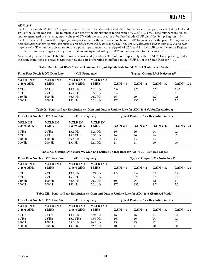
AD7715
–13–REV. C
AD7715-3Table IX shows the AD7715-3 output rms noise for the selectable notch and –3 dB frequencies for the part, as selected by FS1 andFS0 of the Setup Register. The numbers given are for the bipolar input ranges with a VREF of +1.25 V. These numbers are typicaland are generated at an analog input voltage of 0 V with the part used in unbuffered mode (BUF bit of the Setup Register = 0).Table X meanwhile shows the output peak-to-peak noise for the selectable notch and –3 dB frequencies for the part. It is important tonote that these numbers represent the resolution for which there will be no code flicker. They are not calculated based on rms noise but on peak-to-peak noise. The numbers given are for the bipolar input ranges with a VREF of +1.25 V and for the BUF bit of the Setup Register =0. These numbers are typical, are generated at an analog input voltage of 0 V and are rounded to the nearest LSB.
Meanwhile, Table XI and Table XII show rms noise and peak-to-peak resolution respectively with the AD7715-3 operating underthe same conditions as above except that now the part is operating in buffered mode (BUF Bit of the Setup Register = 1).
Table IX. Output RMS Noise vs. Gain and Output Update Rate for AD7715-3 (Unbuffered Mode)
Filter First Notch & O/P Data Rate –3 dB Frequency Typical Output RMS Noise in mV
MCLK IN = MCLK IN = MCLK IN = MCLK IN =2.4576 MHz 1 MHz 2.4576 MHz 1 MHz GAIN = 1 GAIN = 2 GAIN = 32 GAIN = 128
50 Hz 20 Hz 13.1 Hz 5.24 Hz 3.0 1.7 0.7 0.6560 Hz 25 Hz 15.72 Hz 6.55 Hz 3.4 2.1 0.7 0.7250 Hz 100 Hz 65.5 Hz 26.2 Hz 45 20 2.2 1.6500 Hz 200 Hz 131 Hz 52.4 Hz 270 135 9.7 3.3
Table X. Peak-to-Peak Resolution vs. Gain and Output Update Rate for AD7715-3 (Unbuffered Mode)
Filter First Notch & O/P Data Rate –3 dB Frequency Typical Peak-to-Peak Resolution in Bits
MCLK IN = MCLK IN = MCLK IN = MCLK IN =2.4576 MHz 1 MHz 2.4576 MHz 1 MHz GAIN = 1 GAIN = 2 GAIN = 32 GAIN = 128
50 Hz 20 Hz 13.1 Hz 5.24 Hz 16 16 14 1260 Hz 25 Hz 15.72 Hz 6.55 Hz 16 16 14 12250 Hz 100 Hz 65.5 Hz 26.2 Hz 13 13 13 11500 Hz 200 Hz 131 Hz 52.4 Hz 11 11 10 10
Table XI. Output RMS Noise vs. Gain and Output Update Rate for AD7715-3 (Buffered Mode)
Filter First Notch & O/P Data Rate –3 dB Frequency Typical Output RMS Noise in mV
MCLK IN = MCLK IN = MCLK IN = MCLK IN =2.4576 MHz 1 MHz 2.4576 MHz 1 MHz GAIN = 1 GAIN = 2 GAIN = 32 GAIN = 128
50 Hz 20 Hz 13.1 Hz 5.24 Hz 4.5 2.4 0.9 0.960 Hz 25 Hz 15.72 Hz 6.55 Hz 5.1 2.9 0.9 1.0250 Hz 100 Hz 65.5 Hz 26.2 Hz 50 25 2.6 2500 Hz 200 Hz 131 Hz 52.4 Hz 270 135 9.7 3.3
Table XII. Peak-to-Peak Resolution vs. Gain and Output Update Rate for AD7715-3 (Buffered Mode)
Filter First Notch & O/P Data Rate –3 dB Frequency Typical Peak-to-Peak Resolution in Bits
MCLK IN = MCLK IN = MCLK IN = MCLK IN =2.4576 MHz 1 MHz 2.4576 MHz 1 MHz GAIN = 1 GAIN = 2 GAIN = 32 GAIN = 128
50 Hz 20 Hz 13.1 Hz 5.24 Hz 16 16 14 1260 Hz 25 Hz 15.72 Hz 6.55 Hz 16 16 14 12250 Hz 100 Hz 65.5 Hz 26.2 Hz 13 13 12 11500 Hz 200 Hz 131 Hz 52.4 Hz 10 11 10 10
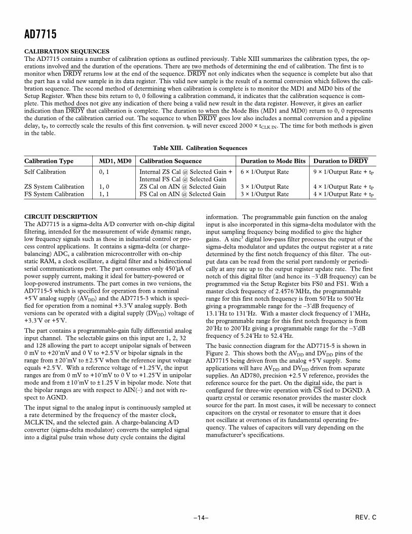
REV. C
AD7715
–14–
CALIBRATION SEQUENCESThe AD7715 contains a number of calibration options as outlined previously. Table XIII summarizes the calibration types, the op-erations involved and the duration of the operations. There are two methods of determining the end of calibration. The first is tomonitor when DRDY returns low at the end of the sequence. DRDY not only indicates when the sequence is complete but also thatthe part has a valid new sample in its data register. This valid new sample is the result of a normal conversion which follows the cali-bration sequence. The second method of determining when calibration is complete is to monitor the MD1 and MD0 bits of theSetup Register. When these bits return to 0, 0 following a calibration command, it indicates that the calibration sequence is com-plete. This method does not give any indication of there being a valid new result in the data register. However, it gives an earlierindication than DRDY that calibration is complete. The duration to when the Mode Bits (MD1 and MD0) return to 0, 0 representsthe duration of the calibration carried out. The sequence to when DRDY goes low also includes a normal conversion and a pipelinedelay, tP, to correctly scale the results of this first conversion. tP will never exceed 2000 × tCLK IN. The time for both methods is givenin the table.
Table XIII. Calibration Sequences
Calibration Type MD1, MD0 Calibration Sequence Duration to Mode Bits Duration to DRDY
Self Calibration 0, 1 Internal ZS Cal @ Selected Gain + 6 × 1/Output Rate 9 × 1/Output Rate + tP
Internal FS Cal @ Selected GainZS System Calibration 1, 0 ZS Cal on AIN @ Selected Gain 3 × 1/Output Rate 4 × 1/Output Rate + tP
FS System Calibration 1, 1 FS Cal on AIN @ Selected Gain 3 × 1/Output Rate 4 × 1/Output Rate + tP
CIRCUIT DESCRIPTIONThe AD7715 is a sigma-delta A/D converter with on-chip digitalfiltering, intended for the measurement of wide dynamic range,low frequency signals such as those in industrial control or pro-cess control applications. It contains a sigma-delta (or charge-balancing) ADC, a calibration microcontroller with on-chipstatic RAM, a clock oscillator, a digital filter and a bidirectionalserial communications port. The part consumes only 450 µA ofpower supply current, making it ideal for battery-powered orloop-powered instruments. The part comes in two versions, theAD7715-5 which is specified for operation from a nominal+5 V analog supply (AVDD) and the AD7715-3 which is speci-fied for operation from a nominal +3.3 V analog supply. Bothversions can be operated with a digital supply (DVDD) voltage of+3.3 V or +5 V.
The part contains a programmable-gain fully differential analoginput channel. The selectable gains on this input are 1, 2, 32and 128 allowing the part to accept unipolar signals of between0 mV to +20 mV and 0 V to +2.5 V or bipolar signals in therange from ±20 mV to ±2.5 V when the reference input voltageequals +2.5 V. With a reference voltage of +1.25 V, the inputranges are from 0 mV to +10 mV to 0 V to +1.25 V in unipolarmode and from ±10 mV to ±1.25 V in bipolar mode. Note thatthe bipolar ranges are with respect to AIN(–) and not with re-spect to AGND.
The input signal to the analog input is continuously sampled ata rate determined by the frequency of the master clock,MCLK IN, and the selected gain. A charge-balancing A/Dconverter (sigma-delta modulator) converts the sampled signalinto a digital pulse train whose duty cycle contains the digital
information. The programmable gain function on the analoginput is also incorporated in this sigma-delta modulator with theinput sampling frequency being modified to give the highergains. A sinc3 digital low-pass filter processes the output of thesigma-delta modulator and updates the output register at a ratedetermined by the first notch frequency of this filter. The out-put data can be read from the serial port randomly or periodi-cally at any rate up to the output register update rate. The firstnotch of this digital filter (and hence its –3 dB frequency) can beprogrammed via the Setup Register bits FS0 and FS1. With amaster clock frequency of 2.4576 MHz, the programmablerange for this first notch frequency is from 50 Hz to 500 Hzgiving a programmable range for the –3 dB frequency of13.1 Hz to 131 Hz. With a master clock frequency of 1 MHz,the programmable range for this first notch frequency is from20 Hz to 200 Hz giving a programmable range for the –3 dBfrequency of 5.24 Hz to 52.4 Hz.
The basic connection diagram for the AD7715-5 is shown inFigure 2. This shows both the AVDD and DVDD pins of theAD7715 being driven from the analog +5 V supply. Someapplications will have AVDD and DVDD driven from separatesupplies. An AD780, precision +2.5 V reference, provides thereference source for the part. On the digital side, the part isconfigured for three-wire operation with CS tied to DGND. Aquartz crystal or ceramic resonator provides the master clocksource for the part. In most cases, it will be necessary to connectcapacitors on the crystal or resonator to ensure that it doesnot oscillate at overtones of its fundamental operating fre-quency. The values of capacitors will vary depending on themanufacturer’s specifications.
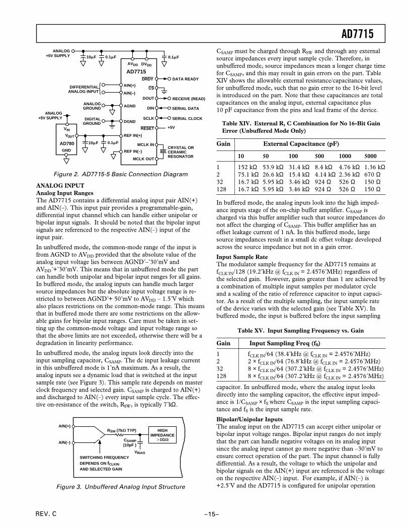
AD7715
–15–REV. C
CSAMP must be charged through RSW and through any externalsource impedances every input sample cycle. Therefore, inunbuffered mode, source impedances mean a longer charge timefor CSAMP, and this may result in gain errors on the part. TableXIV shows the allowable external resistance/capacitance values,for unbuffered mode, such that no gain error to the 16-bit levelis introduced on the part. Note that these capacitances are totalcapacitances on the analog input, external capacitance plus10 pF capacitance from the pins and lead frame of the device.
Table XIV. External R, C Combination for No 16-Bit GainError (Unbuffered Mode Only)
Gain External Capacitance (pF)
10 50 100 500 1000 5000
1 152 kΩ 53.9 kΩ 31.4 kΩ 8.4 kΩ 4.76 kΩ 1.36 kΩ2 75.1 kΩ 26.6 kΩ 15.4 kΩ 4.14 kΩ 2.36 kΩ 670 Ω32 16.7 kΩ 5.95 kΩ 3.46 kΩ 924 Ω 526 Ω 150 Ω128 16.7 kΩ 5.95 kΩ 3.46 kΩ 924 Ω 526 Ω 150 Ω
In buffered mode, the analog inputs look into the high imped-ance inputs stage of the on-chip buffer amplifier. CSAMP ischarged via this buffer amplifier such that source impedances donot affect the charging of CSAMP. This buffer amplifier has anoffset leakage current of 1 nA. In this buffered mode, largesource impedances result in a small dc offset voltage developedacross the source impedance but not in a gain error.
Input Sample RateThe modulator sample frequency for the AD7715 remains atfCLK IN/128 (19.2 kHz @ fCLK IN = 2.4576 MHz) regardless ofthe selected gain. However, gains greater than 1 are achieved bya combination of multiple input samples per modulator cycleand a scaling of the ratio of reference capacitor to input capaci-tor. As a result of the multiple sampling, the input sample rateof the device varies with the selected gain (see Table XV). Inbuffered mode, the input is buffered before the input sampling
Table XV. Input Sampling Frequency vs. Gain
Gain Input Sampling Freq (fS)
1 fCLK IN/64 (38.4 kHz @ fCLK IN = 2.4576 MHz)2 2 × fCLK IN/64 (76.8 kHz @ fCLK IN = 2.4576 MHz)32 8 × fCLK IN/64 (307.2 kHz @ fCLK IN = 2.4576 MHz)128 8 × fCLK IN/64 (307.2 kHz @ fCLK IN = 2.4576 MHz)
capacitor. In unbuffered mode, where the analog input looksdirectly into the sampling capacitor, the effective input imped-ance is 1/CSAMP × fS where CSAMP is the input sampling capaci-tance and fS is the input sample rate.
Bipolar/Unipolar InputsThe analog input on the AD7715 can accept either unipolar orbipolar input voltage ranges. Bipolar input ranges do not implythat the part can handle negative voltages on its analog inputsince the analog input cannot go more negative than –30 mV toensure correct operation of the part. The input channel is fullydifferential. As a result, the voltage to which the unipolar andbipolar signals on the AIN(+) input are referenced is the voltageon the respective AIN(–) input. For example, if AIN(–) is+2.5 V and the AD7715 is configured for unipolar operation
SCLK
MCLK IN
DGND
DVDD
MCLK OUT
DIN
DOUT
AGND
AIN(+)
AIN(–)
REF IN(+)
REF IN(–)
AVDD
AD7715
0.1mF
ANALOGGROUND
DIFFERENTIALANALOG INPUT
DIGITALGROUND
0.1mF10mF
VOUT
VIN
GND
AD780
ANALOG+5V SUPPLY
DATA READY
RECEIVE (READ)
SERIAL DATA
SERIAL CLOCK
CRYSTAL ORCERAMICRESONATOR
+5V
0.1mF10mF
ANALOG+5V SUPPLY
RESET
CS
DRDY
Figure 2. AD7715-5 Basic Connection Diagram
ANALOG INPUTAnalog Input RangesThe AD7715 contains a differential analog input pair AIN(+)and AIN(–). This input pair provides a programmable-gain,differential input channel which can handle either unipolar orbipolar input signals. It should be noted that the bipolar inputsignals are referenced to the respective AIN(–) input of theinput pair.
In unbuffered mode, the common-mode range of the input isfrom AGND to AVDD provided that the absolute value of theanalog input voltage lies between AGND – 30 mV andAVDD + 30 mV. This means that in unbuffered mode the partcan handle both unipolar and bipolar input ranges for all gains.In buffered mode, the analog inputs can handle much largersource impedances but the absolute input voltage range is re-stricted to between AGND + 50 mV to AVDD – 1.5 V whichalso places restrictions on the common-mode range. This meansthat in buffered mode there are some restrictions on the allow-able gains for bipolar input ranges. Care must be taken in set-ting up the common-mode voltage and input voltage range sothat the above limits are not exceeded, otherwise there will be adegradation in linearity performance.
In unbuffered mode, the analog inputs look directly into theinput sampling capacitor, CSAMP. The dc input leakage currentin this unbuffered mode is 1 nA maximum. As a result, theanalog inputs see a dynamic load that is switched at the inputsample rate (see Figure 3). This sample rate depends on masterclock frequency and selected gain. CSAMP is charged to AIN(+)and discharged to AIN(–) every input sample cycle. The effec-tive on-resistance of the switch, RSW, is typically 7 kΩ.
HIGHIMPEDANCE
1GV
RSW (7kV TYP)
CSAMP(10pF )
VBIASSWITCHING FREQUENCYDEPENDS ON fCLKIN
AND SELECTED GAIN
AIN(+)
AIN(–)
Figure 3. Unbuffered Analog Input Structure
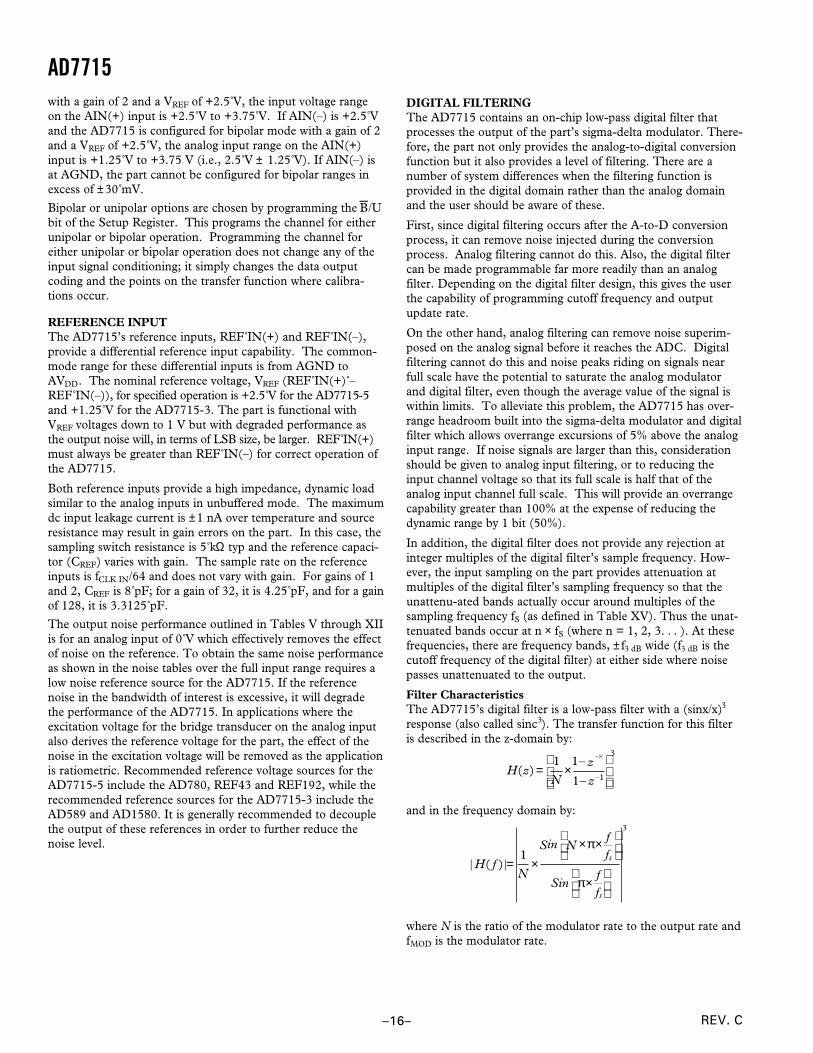
REV. C
AD7715
–16–
DIGITAL FILTERINGThe AD7715 contains an on-chip low-pass digital filter thatprocesses the output of the part’s sigma-delta modulator. There-fore, the part not only provides the analog-to-digital conversionfunction but it also provides a level of filtering. There are anumber of system differences when the filtering function isprovided in the digital domain rather than the analog domainand the user should be aware of these.
First, since digital filtering occurs after the A-to-D conversionprocess, it can remove noise injected during the conversionprocess. Analog filtering cannot do this. Also, the digital filtercan be made programmable far more readily than an analogfilter. Depending on the digital filter design, this gives the userthe capability of programming cutoff frequency and outputupdate rate.
On the other hand, analog filtering can remove noise superim-posed on the analog signal before it reaches the ADC. Digitalfiltering cannot do this and noise peaks riding on signals nearfull scale have the potential to saturate the analog modulatorand digital filter, even though the average value of the signal iswithin limits. To alleviate this problem, the AD7715 has over-range headroom built into the sigma-delta modulator and digitalfilter which allows overrange excursions of 5% above the analoginput range. If noise signals are larger than this, considerationshould be given to analog input filtering, or to reducing theinput channel voltage so that its full scale is half that of theanalog input channel full scale. This will provide an overrangecapability greater than 100% at the expense of reducing thedynamic range by 1 bit (50%).
In addition, the digital filter does not provide any rejection atinteger multiples of the digital filter’s sample frequency. How-ever, the input sampling on the part provides attenuation atmultiples of the digital filter’s sampling frequency so that theunattenu-ated bands actually occur around multiples of thesampling frequency fS (as defined in Table XV). Thus the unat-tenuated bands occur at n × fS (where n = 1, 2, 3. . . ). At thesefrequencies, there are frequency bands, ± f3 dB wide (f3 dB is thecutoff frequency of the digital filter) at either side where noisepasses unattenuated to the output.
Filter CharacteristicsThe AD7715’s digital filter is a low-pass filter with a (sinx/x)3
response (also called sinc3). The transfer function for this filteris described in the z-domain by:
and in the frequency domain by:
where N is the ratio of the modulator rate to the output rate andfMOD is the modulator rate.
with a gain of 2 and a VREF of +2.5 V, the input voltage rangeon the AIN(+) input is +2.5 V to +3.75 V. If AIN(–) is +2.5 Vand the AD7715 is configured for bipolar mode with a gain of 2and a VREF of +2.5 V, the analog input range on the AIN(+)input is +1.25 V to +3.75 V (i.e., 2.5 V ± 1.25 V). If AIN(–) isat AGND, the part cannot be configured for bipolar ranges inexcess of ±30 mV.
Bipolar or unipolar options are chosen by programming the B/Ubit of the Setup Register. This programs the channel for eitherunipolar or bipolar operation. Programming the channel foreither unipolar or bipolar operation does not change any of theinput signal conditioning; it simply changes the data outputcoding and the points on the transfer function where calibra-tions occur.
REFERENCE INPUTThe AD7715’s reference inputs, REF IN(+) and REF IN(–),provide a differential reference input capability. The common-mode range for these differential inputs is from AGND toAVDD. The nominal reference voltage, VREF (REF IN(+) –REF IN(–)), for specified operation is +2.5 V for the AD7715-5and +1.25 V for the AD7715-3. The part is functional withVREF voltages down to 1 V but with degraded performance asthe output noise will, in terms of LSB size, be larger. REF IN(+)must always be greater than REF IN(–) for correct operation ofthe AD7715.
Both reference inputs provide a high impedance, dynamic loadsimilar to the analog inputs in unbuffered mode. The maximumdc input leakage current is ±1 nA over temperature and sourceresistance may result in gain errors on the part. In this case, thesampling switch resistance is 5 kΩ typ and the reference capaci-tor (CREF) varies with gain. The sample rate on the referenceinputs is fCLK IN/64 and does not vary with gain. For gains of 1and 2, CREF is 8 pF; for a gain of 32, it is 4.25 pF, and for a gainof 128, it is 3.3125 pF.
The output noise performance outlined in Tables V through XIIis for an analog input of 0 V which effectively removes the effectof noise on the reference. To obtain the same noise performanceas shown in the noise tables over the full input range requires alow noise reference source for the AD7715. If the referencenoise in the bandwidth of interest is excessive, it will degradethe performance of the AD7715. In applications where theexcitation voltage for the bridge transducer on the analog inputalso derives the reference voltage for the part, the effect of thenoise in the excitation voltage will be removed as the applicationis ratiometric. Recommended reference voltage sources for theAD7715-5 include the AD780, REF43 and REF192, while therecommended reference sources for the AD7715-3 include theAD589 and AD1580. It is generally recommended to decouplethe output of these references in order to further reduce thenoise level.
H z
Nz
z
N
( )–
– –= ×
−1 1
1 1
3
| ( )|H fN
Sin Nff
Sinff
s
s
= ×× ×
×
1
3
π
π
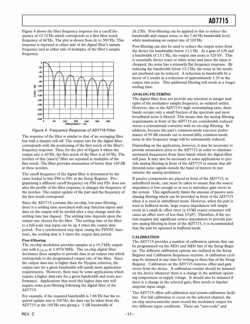
AD7715
–17–REV. C
Figure 4 shows the filter frequency response for a cutoff fre-quency of 15.72 Hz which corresponds to a first filter notchfrequency of 60 Hz. The plot is shown from dc to 390 Hz. Thisresponse is repeated at either side of the digital filter’s samplefrequency and at either side of multiples of the filter’s samplefrequency.
FREQUENCY – Hz
0
–40
–60
–80
–100
–120
–140
–160
–180
–200
–220
–20
–2403600 30018012060 240
GA
IN –
dB
Figure 4. Frequency Response of AD7715 Filter
The response of the filter is similar to that of an averaging filterbut with a sharper roll-off. The output rate for the digital filtercorresponds with the positioning of the first notch of the filter’sfrequency response. Thus, for the plot of Figure 4 where theoutput rate is 60 Hz, the first notch of the filter is at 60 Hz. Thenotches of this (sinx/x)3 filter are repeated at multiples of thefirst notch. The filter provides attenuation of better than 100 dBat these notches.
The cutoff frequency of the digital filter is determined by thevalue loaded to bits FS0 to FS1 in the Setup Register. Pro-gramming a different cutoff frequency via FS0 and FS1 does notalter the profile of the filter response; it changes the frequency ofthe notches. The output update of the part and the frequency ofthe first notch correspond.
Since the AD7715 contains this on-chip, low-pass filtering,there is a settling time associated with step function inputs anddata on the output will be invalid after a step change until thesettling time has elapsed. The settling time depends upon theoutput rate chosen for the filter. The settling time of the filterto a full-scale step input can be up 4 times the output dataperiod. For a synchronized step input (using the FSYNC func-tion), the settling time is 3 times the output data period.
Post-FilteringThe on-chip modulator provides samples at a 19.2 kHz outputrate with fCLK IN at 2.4576 MHz. The on-chip digital filterdecimates these samples to provide data at an output rate whichcorresponds to the programmed output rate of the filter. Sincethe output data rate is higher than the Nyquist criterion, theoutput rate for a given bandwidth will satisfy most applicationrequirements. However, there may be some applications whichrequire a higher data rate for a given bandwidth and noise per-formance. Applications that need this higher data rate willrequire some post-filtering following the digital filter of theAD7715.
For example, if the required bandwidth is 7.86 Hz but the re-quired update rate is 100 Hz, the data can be taken from theAD7715 at the 100 Hz rate giving a –3 dB bandwidth of
26.2 Hz. Post-filtering can be applied to this to reduce thebandwidth and output noise, to the 7.86 Hz bandwidth level,while maintaining an output rate of 100 Hz.
Post-filtering can also be used to reduce the output noise fromthe device for bandwidths below 13.1 Hz. At a gain of 128 anda bandwidth of 13.1 Hz, the output rms noise is 520 nV. Thisis essentially device noise or white noise and since the input ischopped, the noise has a primarily flat frequency response. Byreducing the bandwidth below 13.1 Hz, the noise in the result-ant passband can be reduced. A reduction in bandwidth by afactor of 2 results in a reduction of approximately 1.25 in theoutput rms noise. This additional filtering will result in a longersettling time.
ANALOG FILTERINGThe digital filter does not provide any rejection at integer mul-tiples of the modulator sample frequency, as outlined earlier.However, due to the AD7715’s high oversampling ratio, thesebands occupy only a small fraction of the spectrum and mostbroadband noise is filtered. This means that the analog filteringrequirements in front of the AD7715 are considerably reducedversus a conventional converter with no on-chip filtering. Inaddition, because the part’s common-mode rejection perfor-mance of 95 dB extends out to several kHz, common-modenoise in this frequency range will be substantially reduced.
Depending on the application, however, it may be necessary toprovide attenuation prior to the AD7715 in order to eliminateunwanted frequencies from these bands which the digital filterwill pass. It may also be necessary in some applications to pro-vide analog filtering in front of the AD7715 to ensure that dif-ferential noise signals outside the band of interest do notsaturate the analog modulator.
If passive components are placed in front of the AD7715, inunbuffered mode, care must be taken to ensure that the sourceimpedance is low enough so as not to introduce gain errors inthe system. This significantly limits the amount of passive anti-aliasing filtering which can be provided in front of the AD7715when it is used in unbuffered mode. However, when the part isused in buffered mode, large source impedances will simplyresult in a small dc offset error (a 10 kΩ source resistance willcause an offset error of less than 10 µV). Therefore, if the sys-tem requires any significant source impedances to provide pas-sive analog filtering in front of the AD7715, it is recommendedthat the part be operated in buffered mode.
CALIBRATIONThe AD7715 provides a number of calibration options that canbe programmed via the MD1 and MD0 bits of the Setup Regis-ter. The different calibration options are outlined in the SetupRegister and Calibration Sequences sections. A calibration cyclemay be initiated at any time by writing to these bits of the SetupRegister. Calibration on the AD7715 removes offset and gainerrors from the device. A calibration routine should be initiatedon the device whenever there is a change in the ambient operat-ing temperature or supply voltage. It should also be initiated ifthere is a change in the selected gain, filter notch or bipolar/unipolar input range.
The AD7715 offers self-calibration and system-calibration facili-ties. For full calibration to occur on the selected channel, theon-chip microcontroller must record the modulator output fortwo different input conditions. These are “zero-scale” and
REV. C
AD7715
–18–
“full-scale” points. These points are derived by performing aconversion on the different input voltages provided to the inputof the modulator during calibration. As a result, the accuracy ofthe calibration can only be as good as the noise level that itprovides in normal mode. The result of the “zero-scale” calibra-tion conversion is stored in the Zero-Scale Calibration Registerwhile the result of the “full-scale” calibration conversion isstored in the Full-Scale Calibration Register. With these read-ings, the on-chip microcontroller can calculate the offset and thegain slope for the input to output transfer function of the con-verter. Internally, the part works with a resolution of 33 bits todetermine its conversion result of 16 bits.
Self-CalibrationA self-calibration is initiated on the AD7715 by writing theappropriate values (0, 1) to the MD1 and MD0 bits of theSetup Register. In the self-calibration mode with a unipolarinput range, the zero-scale point used in determining the cali-bration coefficients is with the inputs of the differential pairinternally shorted on the part (i.e., AIN(+) = AIN(–) = InternalBias Voltage). The PGA is set for the selected gain (as per G1and G0 bits in the Communications Register) for this zero-scalecalibration conversion. The full-scale calibration conversion isperformed at the selected gain on an internally generated voltageof VREF/Selected Gain.
The duration time for the calibration is 6 × 1/Output Rate. Thisis made up of 3 × 1/Output Rate for the zero-scale calibrationand 3 × 1/Output Rate for the full-scale calibration. At this timethe MD1 and MD0 bits in the Setup Register return to 0, 0.This gives the earliest indication that the calibration sequence iscomplete. The DRDY line goes high when calibration is initi-ated and does not return low until there is a valid new word inthe data register. The duration time from the calibration com-mand being issued to DRDY going low is 9 × 1/Output Rate.This is made up of 3 × 1/Output Rate for the zero-scale calibra-tion, 3 × 1/Output Rate for the full-scale calibration, 3 × 1/Output Rate for a conversion on the analog input and someoverhead to set up the coefficients correctly. If DRDY is lowbefore (or goes low during) the calibration command write tothe Setup Register, it may take up to one modulator cycle(MCLK IN/128) before DRDY goes high to indicate that cali-bration is in progress. Therefore, DRDY should be ignored forup to one modulator cycle after the last bit is written to theSetup Register in the calibration command.
For bipolar input ranges in the self-calibrating mode, the se-quence is very similar to that just outlined. In this case, the twopoints are exactly the same as above, but since the part is config-ured for bipolar operation, the shorted inputs point is actuallymidscale of the transfer function.
System CalibrationSystem calibration allows the AD7715 to compensate for systemgain and offset errors as well as its own internal errors. Systemcalibration performs the same slope factor calculations as self-calibration but uses voltage values presented by the system tothe AIN inputs for the zero- and full-scale points. Full Systemcalibration requires a two step process, a ZS System Calibrationfollowed by a FS System Calibration.
For a full system calibration, the zero-scale point must be pre-sented to the converter first. It must be applied to the converterbefore the calibration step is initiated and remain stable until the
step is complete. Once the system zero scale voltage has been setup, a ZS System Calibration is then initiated by writing the ap-propriate values (1, 0) to the MD1 and MD0 bits of the SetupRegister. The zero-scale system calibration is performed at theselected gain. The duration of the calibration is 3 × 1/OutputRate. At this time the MD1 and MD0 bits in the Setup Registerreturn to 0, 0. This gives the earliest indication that the calibrationsequence is complete. The DRDY line goes high when calibrationis initiated and does not return low until there is a valid newword in the data register. The duration time from the calibra-tion command being issued to DRDY going low is 4 × 1/OutputRate as the part performs a normal conversion on the AIN volt-age before DRDY goes low. If DRDY is low before (or goes lowduring) the calibration command write to the Setup Register, itmay take up to one modulator cycle (MCLK IN/128) beforeDRDY goes high to indicate that calibration is in progress.Therefore, DRDY should be ignored for up to one modulatorcycle after the last bit is written to the Setup Register in thecalibration command.
After the zero-scale point is calibrated, the full-scale point isapplied to AIN and the second step of the calibration process isinitiated by again writing the appropriate values (1, 1) to MD1and MD0. Again the full-scale voltage must be set up beforethe calibration is initiated and it must remain stable throughoutthe calibration step. The full-scale system calibration is per-formed at the selected gain. The duration of the calibration is3 × 1/Output Rate. At this time the MD1 and MD0 bits in theSetup Register return to 0, 0. This gives the earliest indicationthat the calibration sequence is complete. The DRDY line goeshigh when calibration is initiated and does not return low untilthere is a valid new word in the data register. The duration timefrom the calibration command being issued to DRDY going lowis 4 × 1/Output Rate as the part performs a normal conversionon the AIN voltage before DRDY goes low. If DRDY is lowbefore (or goes low during) the calibration command, write tothe Setup Register, it may take up to one modulator cycle(MCLK IN/128) before DRDY goes high to indicate that cali-bration is in progress. Therefore, DRDY should be ignored forup to one modulator cycle after the last bit is written to theSetup Register in the calibration command.
In the unipolar mode, the system calibration is performed be-tween the two endpoints of the transfer function; in the bipolarmode, it is performed between midscale (zero differential volt-age) and positive full scale.
The fact that the system calibration is a two-step calibrationoffers another feature. After the sequence of a full system cali-bration has been completed, additional offset or gain calibra-tions can be performed by themselves to adjust the system zeroreference point or the system gain. Calibrating one of the pa-rameters, either system offset or system gain, will not affect theother parameter.
System calibration can also be used to remove any errors fromsource impedances on the analog input when the part is used inunbuffered mode. A simple R, C antialiasing filter on the frontend may introduce a gain error on the analog input voltage butthe system calibration can be used to remove this error.
Span and Offset LimitsWhenever a system calibration mode is used, there are limits onthe amount of offset and span which can be accommodated.The overriding requirement in determining the amount of offset
AD7715
–19–REV. C
and gain that can be accommodated by the part is the require-ment that the positive full-scale calibration limit is ≤ 1.05 ×VREF/GAIN. This allows the input range to go 5% above thenominal range. The in-built headroom in the AD7715’s analogmodulator ensures that the part will still operate correctly with apositive full-scale voltage which is 5% beyond the nominal.
The range of input span in both the unipolar and bipolar modeshas a minimum value of 0.8 × VREF/GAIN and a maximumvalue of 2.1 × VREF/GAIN. However, the span (which is thedifference between the bottom of the AD7715’s input range andthe top of its input range) must take into account the limitationon the positive full-scale voltage. The amount of offset that canbe accommodated depends on whether the unipolar or bipolarmode is being used. Once again, the offset must take into ac-count the limitation on the positive full-scale voltage. In unipo-lar mode, there is considerable flexibility in handling negative(with respect to AIN(–)) offsets. In both unipolar and bipolarmodes, the range of positive offsets which can be handled by thepart depends on the selected span. Therefore, in determiningthe limits for system zero-scale and full-scale calibrations, theuser has to ensure that the offset range plus the span range doesexceed 1.05 × VREF/GAIN. This is best illustrated by looking ata few examples.
If the part is used in unipolar mode with a required span of0.8 × VREF/GAIN, then the offset range which the system cali-bration can handle is from –1.05 × VREF/GAIN to +0.25 × VREF/GAIN. If the part is used in unipolar mode with a required span ofVREF/GAIN, then the offset range which the system calibration canhandle is from –1.05 × VREF/GAIN to +0.05 × VREF/GAIN. Simi-larly, if the part is used in unipolar mode and required to re-move an offset of 0.2 × VREF/GAIN, then the span range whichthe system calibration can handle is 0.85 × VREF/GAIN.
If the part is used in bipolar mode with a required span of±0.4 × VREF/GAIN, then the offset range which the system cali-bration can handle is from –0.65 × VREF/GAIN to +0.65 × VREF/GAIN. If the part is used in bipolar mode with a required spanof ±VREF/GAIN, then the offset range which the system calibra-tion can handle is from –0.05 × VREF/GAIN to +0.05 × VREF/GAIN. Similarly, if the part is used in bipolar mode and requiredto remove an offset of ±0.2 × VREF/GAIN, then the span rangewhich the system calibration can handle is ±0.85 × VREF/GAIN.
Power-Up and CalibrationOn power-up, the AD7715 performs an internal reset that setsthe contents of the internal registers to a known state. Thereare default values loaded to all registers after a power-on orreset. The default values contain nominal calibration coefficientsfor the calibration registers. However, to ensure correct calibra-tion for the device a calibration routine should be performedafter power-up.
The power dissipation and temperature drift of the AD7715 arelow, and no warm-up time is required before the initial calibra-tion is performed. However, if an external reference is beingused, this reference must have stabilized before calibration isinitiated. Similarly, if the clock source for the part is generatedfrom a crystal or resonator across the MCLK pins, the start-uptime for the oscillator circuit should elapse before a calibrationis initiated on the part (see below).
USING THE AD7715Clocking and Oscillator CircuitThe AD7715 requires a master clock input, which may be anexternal CMOS compatible clock signal applied to the MCLK INpin with the MCLK OUT pin left unconnected. Alternatively, acrystal or ceramic resonator of the correct frequency can beconnected between MCLK IN and MCLK OUT in which casethe clock circuit will function as an oscillator, providing theclock source for the part. The input sampling frequency, themodulator sampling frequency, the –3 dB frequency, outputupdate rate and calibration time are all directly related to themaster clock frequency, fCLK IN. Reducing the master clockfrequency by a factor of 2 will halve the above frequencies andupdate rate and double the calibration time. The current drawnfrom the DVDD power supply is also directly related to fCLK IN.Reducing fCLK IN by a factor of 2 will halve the DVDD currentbut will not affect the current drawn from the AVDD powersupply.
Using the part with a crystal or ceramic resonator between theMCLK IN and MCLK OUT pins generally causes more cur-rent to be drawn from DVDD than when the part is clocked froma driven clock signal at the MCLK IN pin. This is because theon-chip oscillator circuit is active in the case of the crystal orceramic resonator. Therefore, the lowest possible current onthe AD7715 is achieved with an externally applied clock at theMCLK IN pin with MCLK OUT unconnected and unloaded.
The amount of additional current taken by the oscillator de-pends on a number of factors—first, the larger the value ofcapacitor placed on the MCLK IN and MCLK OUT pins, thenthe larger the DVDD current consumption on the AD7715. Careshould be taken not to exceed the capacitor values recommendedby the crystal and ceramic resonator manufacturers to avoidconsuming unnecessary DVDD current. Typical values recom-mended by crystal or ceramic resonator manufacturers are in therange of 30 pF to 50 pF, and if the capacitor values on MCLKIN and MCLK OUT are kept in this range, they will not resultin any excessive DVDD current. Another factor that influencesthe DVDD current is the effective series resistance (ESR) of thecrystal which appears between the MCLK IN and MCLK OUTpins of the AD7715. As a general rule, the lower the ESR valuethen the lower the current taken by the oscillator circuit.
When operating with a clock frequency of 2.4576 MHz, there is50 µA difference in the DVDD current between an externallyapplied clock and a crystal resonator when operating with aDVDD of +3 V. With DVDD = +5 V and fCLK IN = 2.4576 MHz,the typical DVDD current increases by 200 µA for a crystal/resonator supplied clock versus an externally applied clock. TheESR values for crystals and resonators at this frequency tend tobe low and as a result there tends to be little difference betweendifferent crystal and resonator types.
When operating with a clock frequency of 1 MHz, the ESR valuefor different crystal types varies significantly. As a result, the DVDD
current drain varies across crystal types. When using a crystalwith an ESR of 700 Ω or when using a ceramic resonator, theincrease in the typical DVDD current over an externally-appliedclock is 50 µA with DVDD = +3 V and 175 µA with DVDD =+5 V. When using a crystal with an ESR of 3 kΩ, the increase inthe typical DVDD current over an externally applied clock is100 µA with DVDD = +3 V and 400 µA with DVDD = +5 V.
REV. C
AD7715
–20–
The on-chip oscillator circuit also has a start-up time associatedwith it before it is oscillating at its correct frequency and correctvoltage levels. The typical start-up time for the circuit is 10 mswith a DVDD of +5 V and 15 ms with a DVDD of +3 V. At 3 Vsupplies, depending on the loading capacitances on the MCLKpins, a 1 MΩ feedback resistor may be required across the crys-tal or resonator in order to keep the start up times around the15 ms duration.
The AD7715’s master clock appears on the MCLK OUT pin ofthe device. The maximum recommended load on this pin is oneCMOS load. When using a crystal or ceramic resonator to gen-erate the AD7715’s clock, it may be desirable to then use thisclock as the clock source for the system. In this case, it is recom-mended that the MCLK OUT signal is buffered with a CMOSbuffer before being applied to the rest of the circuit.
System SynchronizationThe FSYNC bit of the Setup Register allows the user to resetthe modulator and digital filter without affecting any of thesetup conditions on the part. This allows the user to start gath-ering samples of the analog input from a known point in time,i.e., when the FSYNC is changed from 1 to 0.
With a 1 in the FSYNC bit of the Setup Register, the digitalfilter and analog modulator are held in a known reset state andthe part is not processing any input samples. When a 0 is thenwritten to the FSYNC bit, the modulator and filter are takenout of this reset state and on the next master clock edge the partstarts to gather samples again.
The FSYNC input can also be used as a software start convertcommand allowing the AD7715 to be operated in a conven-tional converter fashion. In this mode, writing to the FSYNC bitstarts conversion and the falling edge of DRDY indicates whenconversion is complete. The disadvantage of this scheme is thatthe settling time of the filter has to be taken into account forevery data register update. This means that the rate at which thedata register is updated is three times slower in this mode.
Since the FSYNC bit resets the digital filter, the full settlingtime of 3 × 1/Output Rate must elapse before there is a newword loaded to the output register on the part. If the DRDYsignal is low when FSYNC goes to a 0, the DRDY signal willnot be reset high by the FSYNC command. This is because theAD7715 recognizes that there is a word in the data register thathas not been read. The DRDY line will stay low until an updateof the data register takes place at which time it will go high for500 × tCLK IN before returning low again. A read from the dataregister resets the DRDY signal high, and it will not return lowuntil the settling time of the filter has elapsed (from the FSYNCcommand) and there is a valid new word in the data register. Ifthe DRDY line is high when the FSYNC command is issued,the DRDY line will not return low until the settling time of thefilter has elapsed.
Reset InputThe RESET input on the AD7715 resets all the logic, the digitalfilter and the analog modulator while all on-chip registers arereset to their default state. DRDY is driven high and the AD7715ignores all communications to any of its registers while theRESET input is low. When the RESET input returns high, theAD7715 starts to process data, and DRDY will return low in3 × 1/Output Rate indicating a valid new word in the dataregister. However, the AD7715 operates with its default setup
conditions after a RESET and it is generally necessary to set upall registers and carry out a calibration after a RESET command.
The AD7715’s on-chip oscillator circuit continues to functioneven when the RESET input is low. The master clock signalcontinues to be available on the MCLK OUT pin. Therefore, inapplications where the system clock is provided by the AD7715’sclock, the AD7715 produces an uninterrupted master clockduring RESET commands.
Standby ModeThe STBY bit in the Communications Register of the AD7715allows the user to place the part in a power-down mode when itis not required to provide conversion results. The AD7715retains the contents of all its on-chip registers (including thedata register) while in standby mode. When released fromstandby mode, the part starts to process data and a new word isavailable in the data register in 3 × 1/Output Rate from when a 0is written to the STBY bit.
The STBY bit does not affect the digital interface, and it doesnot affect the status of the DRDY line. If DRDY is high whenthe STBY bit is brought low, it will remain high until there is avalid new word in the data register. If DRDY is low when theSTBY bit is brought low, it will remain low until the data regis-ter is updated at which time the DRDY line will return high for500 × tCLK IN before returning low again. If DRDY is low whenthe part enters its standby mode (indicating a valid unread wordin the data register), the data register can be read while the partis in standby. At the end of this read operation, the DRDY willbe reset high as normal.
Placing the part in standby mode reduces the total current to5 µA typical when the part is operated from an external masterclock provided this master clock is stopped. If the external clockcontinues to run in standby mode, the standby current increasesto 150 µA typical with 5 V supplies and 75 µA typical with 3.3 Vsupplies. If a crystal or ceramic resonator is used as the clocksource, then the total current in standby mode is 400 µA typicalwith 5 V supplies and 90 µA with 3.3 V supplies. This is becausethe on-chip oscillator circuit continues to run when the part is inits standby mode. This is important in applications where thesystem clock is provided by the AD7715’s clock, so that theAD7715 produces an uninterrupted master clock even when it isin its standby mode.
AccuracySigma-delta ADCs, like VFCs and other integrating ADCs, donot contain any source of nonmonotonicity and inherently offerno missing codes performance. The AD7715 achieves excellentlinearity by the use of high quality, on-chip capacitors, whichhave a very low capacitance/voltage coefficient. The device alsoachieves low input drift through the use of chopper-stabilizedtechniques in its input stage. To ensure excellent performanceover time and temperature, the AD7715 uses digital calibrationtechniques which minimize offset and gain error.
Drift ConsiderationsThe AD7715 uses chopper stabilization techniques to minimizeinput offset drift. Charge injection in the analog switches anddc leakage currents at the sampling node are the primarysources of offset voltage drift in the converter. The dc inputleakage current is essentially independent of the selected gain.Gain drift within the converter depends primarily upon thetemperature tracking of the internal capacitors. It is not af-fected by leakage currents.
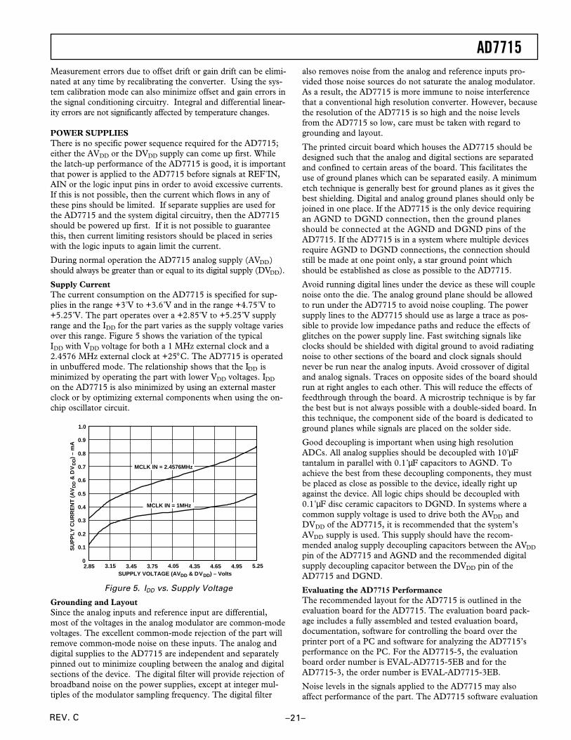
AD7715
–21–REV. C
Measurement errors due to offset drift or gain drift can be elimi-nated at any time by recalibrating the converter. Using the sys-tem calibration mode can also minimize offset and gain errors inthe signal conditioning circuitry. Integral and differential linear-ity errors are not significantly affected by temperature changes.
POWER SUPPLIESThere is no specific power sequence required for the AD7715;either the AVDD or the DVDD supply can come up first. Whilethe latch-up performance of the AD7715 is good, it is importantthat power is applied to the AD7715 before signals at REF IN,AIN or the logic input pins in order to avoid excessive currents.If this is not possible, then the current which flows in any ofthese pins should be limited. If separate supplies are used forthe AD7715 and the system digital circuitry, then the AD7715should be powered up first. If it is not possible to guaranteethis, then current limiting resistors should be placed in serieswith the logic inputs to again limit the current.
During normal operation the AD7715 analog supply (AVDD)should always be greater than or equal to its digital supply (DVDD).
Supply CurrentThe current consumption on the AD7715 is specified for sup-plies in the range +3 V to +3.6 V and in the range +4.75 V to+5.25 V. The part operates over a +2.85 V to +5.25 V supplyrange and the IDD for the part varies as the supply voltage variesover this range. Figure 5 shows the variation of the typicalIDD with VDD voltage for both a 1 MHz external clock and a2.4576 MHz external clock at +25°C. The AD7715 is operatedin unbuffered mode. The relationship shows that the IDD isminimized by operating the part with lower VDD voltages. IDD
on the AD7715 is also minimized by using an external masterclock or by optimizing external components when using the on-chip oscillator circuit.
SUPPLY VOLTAGE (AV DD & DV DD) – Volts
02.85
0.9
1.0
0.8
0.7
0.6
0.5
0.4
0.3
0.2
0.1
3.15 3.45 4.05 4.35 4.65 4.95 5.253.75
MCLK IN = 2.4576MHz
MCLK IN = 1MHz
SU
PP
LY C
UR
RE
NT
(A
VD
D &
DV
DD
) –
mA
Figure 5. IDD vs. Supply Voltage
Grounding and LayoutSince the analog inputs and reference input are differential,most of the voltages in the analog modulator are common-modevoltages. The excellent common-mode rejection of the part willremove common-mode noise on these inputs. The analog anddigital supplies to the AD7715 are independent and separatelypinned out to minimize coupling between the analog and digitalsections of the device. The digital filter will provide rejection ofbroadband noise on the power supplies, except at integer mul-tiples of the modulator sampling frequency. The digital filter
also removes noise from the analog and reference inputs pro-vided those noise sources do not saturate the analog modulator.As a result, the AD7715 is more immune to noise interferencethat a conventional high resolution converter. However, becausethe resolution of the AD7715 is so high and the noise levelsfrom the AD7715 so low, care must be taken with regard togrounding and layout.
The printed circuit board which houses the AD7715 should bedesigned such that the analog and digital sections are separatedand confined to certain areas of the board. This facilitates theuse of ground planes which can be separated easily. A minimumetch technique is generally best for ground planes as it gives thebest shielding. Digital and analog ground planes should only bejoined in one place. If the AD7715 is the only device requiringan AGND to DGND connection, then the ground planesshould be connected at the AGND and DGND pins of theAD7715. If the AD7715 is in a system where multiple devicesrequire AGND to DGND connections, the connection shouldstill be made at one point only, a star ground point whichshould be established as close as possible to the AD7715.
Avoid running digital lines under the device as these will couplenoise onto the die. The analog ground plane should be allowedto run under the AD7715 to avoid noise coupling. The powersupply lines to the AD7715 should use as large a trace as pos-sible to provide low impedance paths and reduce the effects ofglitches on the power supply line. Fast switching signals likeclocks should be shielded with digital ground to avoid radiatingnoise to other sections of the board and clock signals shouldnever be run near the analog inputs. Avoid crossover of digitaland analog signals. Traces on opposite sides of the board shouldrun at right angles to each other. This will reduce the effects offeedthrough through the board. A microstrip technique is by farthe best but is not always possible with a double-sided board. Inthis technique, the component side of the board is dedicated toground planes while signals are placed on the solder side.
Good decoupling is important when using high resolutionADCs. All analog supplies should be decoupled with 10 µFtantalum in parallel with 0.1 µF capacitors to AGND. Toachieve the best from these decoupling components, they mustbe placed as close as possible to the device, ideally right upagainst the device. All logic chips should be decoupled with0.1 µF disc ceramic capacitors to DGND. In systems where acommon supply voltage is used to drive both the AVDD andDVDD of the AD7715, it is recommended that the system’sAVDD supply is used. This supply should have the recom-mended analog supply decoupling capacitors between the AVDD
pin of the AD7715 and AGND and the recommended digitalsupply decoupling capacitor between the DVDD pin of theAD7715 and DGND.
Evaluating the AD7715 PerformanceThe recommended layout for the AD7715 is outlined in theevaluation board for the AD7715. The evaluation board pack-age includes a fully assembled and tested evaluation board,documentation, software for controlling the board over theprinter port of a PC and software for analyzing the AD7715’sperformance on the PC. For the AD7715-5, the evaluationboard order number is EVAL-AD7715-5EB and for theAD7715-3, the order number is EVAL-AD7715-3EB.
Noise levels in the signals applied to the AD7715 may alsoaffect performance of the part. The AD7715 software evaluation
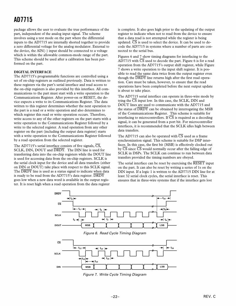
REV. C
AD7715
–22–
package allows the user to evaluate the true performance of thepart, independent of the analog input signal. The schemeinvolves using a test mode on the part where the differentialinputs to the AD7715 are internally shorted together to providea zero differential voltage for the analog modulator. External tothe device, the AIN(–) input should be connected to a voltagewhich is within the allowable common-mode range of the part.This scheme should be used after a calibration has been per-formed on the part.
DIGITAL INTERFACEThe AD7715’s programmable functions are controlled using aset of on-chip registers as outlined previously. Data is written tothese registers via the part’s serial interface and read access tothe on-chip registers is also provided by this interface. All com-munications to the part must start with a write operation to theCommunications Register. After power-on or RESET, the de-vice expects a write to its Communications Register. The datawritten to this register determines whether the next operation tothe part is a read or a write operation and also determines towhich register this read or write operation occurs. Therefore,write access to any of the other registers on the part starts with awrite operation to the Communications Register followed by awrite to the selected register. A read operation from any otherregister on the part (including the output data register) startswith a write operation to the Communications Register followedby a read operation from the selected register.
The AD7715’s serial interface consists of five signals, CS,SCLK, DIN, DOUT and DRDY. The DIN line is used fortransferring data into the on-chip registers while the DOUT lineis used for accessing data from the on-chip registers. SCLK isthe serial clock input for the device and all data transfers (eitheron DIN or DOUT) take place with respect to this SCLK signal.The DRDY line is used as a status signal to indicate when datais ready to be read from the AD7715’s data register. DRDYgoes low when a new data word is available in the output regis-ter. It is reset high when a read operation from the data register
is complete. It also goes high prior to the updating of the outputregister to indicate when not to read from the device to ensurethat a data read is not attempted while the register is beingupdated. CS is used to select the device. It can be used to de-code the AD7715 in systems where a number of parts are con-nected to the serial bus.
Figures 6 and 7 show timing diagrams for interfacing to theAD7715 with CS used to decode the part. Figure 6 is for a readoperation from the AD7715’s output shift register, while Figure7 shows a write operation to the input shift register. It is pos-sible to read the same data twice from the output register eventhough the DRDY line returns high after the first read opera-tion. Care must be taken, however, to ensure that the readoperations have been completed before the next output updateis about to take place.
The AD7715 serial interface can operate in three-wire mode bytying the CS input low. In this case, the SCLK, DIN andDOUT lines are used to communicate with the AD7715 andthe status of DRDY can be obtained by interrogating the MSBof the Communications Register. This scheme is suitable forinterfacing to microcontrollers. If CS is required as a decodingsignal, it can be generated from a port bit. For microcontrollerinterfaces, it is recommended that the SCLK idles high betweendata transfers.
The AD7715 can also be operated with CS used as a framesynchronization signal. This scheme is suitable for DSP inter-faces. In this case, the first bit (MSB) is effectively clocked outby CS since CS would normally occur after the falling edge ofSCLK in DSPs. The SCLK can continue to run between datatransfers provided the timing numbers are obeyed.
The serial interface can be reset by exercising the RESET inputon the part. It can also be reset by writing a series of 1s on theDIN input. If a logic 1 is written to the AD7715 DIN line for atleast 32 serial clock cycles, the serial interface is reset. Thisensures that in three-wire systems that if the interface gets lost
DOUT
SCLK
CS
DRDY
MSB
t5 t7 t9
LSB
t8t6
t3 t10
t4
Figure 6. Read Cycle Timing Diagram
DIN
SCLK
CS
MSB
t12 t15
LSB
t16t14
t13
t11
Figure 7. Write Cycle Timing Diagram
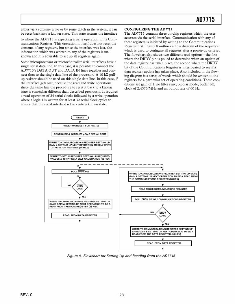
AD7715
–23–REV. C
either via a software error or by some glitch in the system, it canbe reset back into a known state. This state returns the interface
to where the AD7715 is expecting a write operation to its Com-munications Register. This operation in itself does not reset thecontents of any registers, but since the interface was lost, theinformation which was written to any of the registers is un-known and it is advisable to set up all registers again.
Some microprocessor or microcontroller serial interfaces have asingle serial data line. In this case, it is possible to connect theAD7715’s DATA OUT and DATA IN lines together and con-nect then to the single data line of the processor. A 10 kΩ pull-up resistor should be used on this single data line. In this case, ifthe interface gets lost, because the read and write operationsshare the same line the procedure to reset it back to a knownstate is somewhat different than described previously. It requiresa read operation of 24 serial clocks followed by a write operationwhere a logic 1 is written for at least 32 serial clock cycles toensure that the serial interface is back into a known state.
CONFIGURING THE AD7715The AD7715 contains three on-chip registers which the useraccesses via the serial interface. Communication with any ofthese registers is initiated by writing to the CommunicationsRegister first. Figure 8 outlines a flow diagram of the sequencewhich is used to configure all registers after a power-up or reset.The flowchart also shows two different read options—the firstwhere the DRDY pin is polled to determine when an update ofthe data register has taken place, the second where the DRDYbit of the Communications Register is interrogated to see if adata register update has taken place. Also included in the flow-ing diagram is a series of words which should be written to theregisters for a particular set of operating conditions. These con-ditions are gain of 1, no filter sync, bipolar mode, buffer off,clock of 2.4576 MHz and an output rate of 60 Hz.
START
CONFIGURE & INITIALIZE mC/mP SERIAL PORT
POWER-ON/RESET FOR AD7715
WRITE TO COMMUNICATIONS REGISTER SETTING UPGAIN & SETTING UP NEXT OPERATION TO BE A WRITETO THE SETUP REGISTER (10 HEX)
WRITE TO SETUP REGISTER SETTING UP REQUIREDVALUES & INITIATING A SELF CALIBRATION (68 HEX)
POLL DRDY PIN
DRDYLOW?
YES
NO
WRITE TO COMMUNICATIONS REGISTER SETTING UPSAME GAIN & SETTING UP NEXT OPERATION TO BE AREAD FROM THE DATA REGISTER (38 HEX)
READ FROM DATA REGISTER
POLL DRDY BIT OF COMMUNICATIONS REGISTER
YES
NO
WRITE TO COMMUNICATIONS REGISTER SETTING UPSAME GAIN & SETTING UP NEXT OPERATION TO BE AREAD FROM THE DATA REGISTER (38 HEX)
WRITE TO COMMUNICATIONS REGISTER SETTING UP SAMEGAIN & SETTING UP NEXT OPERATION TO BE A READ FROMTHE COMMUNICATIONS REGISTER (08 HEX)
READ FROM COMMUNICATIONS REGISTER
DRDYLOW?
READ FROM DATA REGISTER
Figure 8. Flowchart for Setting Up and Reading from the AD7715
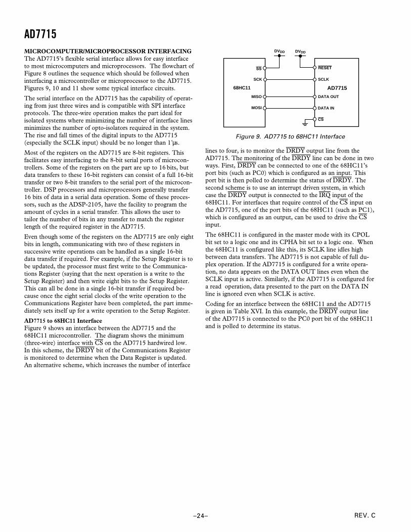
REV. C
AD7715
–24–
MICROCOMPUTER/MICROPROCESSOR INTERFACINGThe AD7715’s flexible serial interface allows for easy interfaceto most microcomputers and microprocessors. The flowchart ofFigure 8 outlines the sequence which should be followed wheninterfacing a microcontroller or microprocessor to the AD7715.Figures 9, 10 and 11 show some typical interface circuits.
The serial interface on the AD7715 has the capability of operat-ing from just three wires and is compatible with SPI interfaceprotocols. The three-wire operation makes the part ideal forisolated systems where minimizing the number of interface linesminimizes the number of opto-isolators required in the system.The rise and fall times of the digital inputs to the AD7715(especially the SCLK input) should be no longer than 1 µs.
Most of the registers on the AD7715 are 8-bit registers. Thisfacilitates easy interfacing to the 8-bit serial ports of microcon-trollers. Some of the registers on the part are up to 16 bits, butdata transfers to these 16-bit registers can consist of a full 16-bittransfer or two 8-bit transfers to the serial port of the microcon-troller. DSP processors and microprocessors generally transfer16 bits of data in a serial data operation. Some of these proces-sors, such as the ADSP-2105, have the facility to program theamount of cycles in a serial transfer. This allows the user totailor the number of bits in any transfer to match the registerlength of the required register in the AD7715.
Even though some of the registers on the AD7715 are only eightbits in length, communicating with two of these registers insuccessive write operations can be handled as a single 16-bitdata transfer if required. For example, if the Setup Register is tobe updated, the processor must first write to the Communica-tions Register (saying that the next operation is a write to theSetup Register) and then write eight bits to the Setup Register.This can all be done in a single 16-bit transfer if required be-cause once the eight serial clocks of the write operation to theCommunications Register have been completed, the part imme-diately sets itself up for a write operation to the Setup Register.
AD7715 to 68HC11 InterfaceFigure 9 shows an interface between the AD7715 and the68HC11 microcontroller. The diagram shows the minimum(three-wire) interface with CS on the AD7715 hardwired low.In this scheme, the DRDY bit of the Communications Registeris monitored to determine when the Data Register is updated.An alternative scheme, which increases the number of interface
AD7715
DATA OUT
SCLK
CS
68HC11
SS
DVDD
RESET
DATA IN
SCK
MISO
MOSI
DVDD
Figure 9. AD7715 to 68HC11 Interface
lines to four, is to monitor the DRDY output line from theAD7715. The monitoring of the DRDY line can be done in twoways. First, DRDY can be connected to one of the 68HC11’sport bits (such as PC0) which is configured as an input. Thisport bit is then polled to determine the status of DRDY. Thesecond scheme is to use an interrupt driven system, in whichcase the DRDY output is connected to the IRQ input of the68HC11. For interfaces that require control of the CS input onthe AD7715, one of the port bits of the 68HC11 (such as PC1),which is configured as an output, can be used to drive the CSinput.
The 68HC11 is configured in the master mode with its CPOLbit set to a logic one and its CPHA bit set to a logic one. Whenthe 68HC11 is configured like this, its SCLK line idles highbetween data transfers. The AD7715 is not capable of full du-plex operation. If the AD7715 is configured for a write opera-tion, no data appears on the DATA OUT lines even when theSCLK input is active. Similarly, if the AD7715 is configured fora read operation, data presented to the part on the DATA INline is ignored even when SCLK is active.
Coding for an interface between the 68HC11 and the AD7715is given in Table XVI. In this example, the DRDY output lineof the AD7715 is connected to the PC0 port bit of the 68HC11and is polled to determine its status.
AD7715
–25–REV. C
AD7715 to 8XC51 InterfaceAn interface circuit between the AD7715 and the 8XC51microcontroller is shown in Figure 10. The diagram shows theminimum number of interface connections with CS on theAD7715 hardwired low. In the case of the 8XC51 interface, theminimum number of interconnects is just two. In this scheme,the DRDY bit of the Communications Register is monitored todetermine when the Data Register is updated. The alternativescheme, which increases the number of interface lines to three,is to monitor the DRDY output line from the AD7715. Themonitoring of the DRDY line can be done in two ways. First,DRDY can be connected to one of the 8XC51’s port bits (suchas P1.0) which is configured as an input. This port bit is thenpolled to determine the status of DRDY. The second scheme isto use an interrupt driven system in which case, the DRDYoutput is connected to the INT1 input of the 8XC51. For inter-faces that require control of the CS input on the AD7715, oneof the port bits of the 8XC51 (such as P1.1), which is config-ured as an output, can be used to drive the CS input.
The 8XC51 is configured in its Mode 0 serial interface mode.Its serial interface contains a single data line. As a result, theDATA OUT and DATA IN pins of the AD7715 should beconnected together with a 10 kΩ pull-up resistor. The serialclock on the 8XC51 idles high between data transfers. The8XC51 outputs the LSB first in a write operation while theAD7715 rearranged before being written to the output serialregister. Similarly, the AD7715 outputs the MSB first during aread operation while the 8XC51 expects the LSB first. There-fore, the data which is read into the serial buffer needs to berearranged before the correct data word from the AD7715 isavailable in the accumulator.
AD7715
DATA OUT
CS
8XC51
RESET
DATA IN
SCLK
P3.0
P3.1
DVDD
DVDD
10kV
Figure 10. AD7715 to 8XC51 Interface
AD7715 to ADSP-2103/ADSP-2105 InterfaceFigure 11 shows an interface between the AD7715 and theADSP-2103/ADSP-2105 DSP processor. In the interfaceshown, the DRDY bit of the Communications Register is againmonitored to determine when the Data Register is updated. Thealternative scheme is to use an interrupt driven system, in whichcase the DRDY output is connected to the IRQ2 input of theADSP-2103/ADSP-2105. The serial interface of the ADSP-2103/ADSP-2105 is set up for alternate framing mode. TheRFS and TFS pins of the ADSP-2103/ADSP-2105 are config-ured as active low outputs, and the ADSP-2103/ADSP-2105serial clock line, SCLK, is also configured as an output. The CSfor the AD7715 is active when either the RFS or TFS outputsfrom the ADSP-2103/ADSP-2105 are active. The serial clockrate on the ADSP-2103/ADSP-2105 should be limited to3 MHz to ensure correct operation with the AD7715.
AD7715
DATA OUT
CS
ADSP-2103/2105
RESET
DATA IN
SCLK
RFS
DR
DT
DVDD
TFS
SCLK
Figure 11. AD7715 to ADSP-2103/ADSP-2105 Interface
CODE FOR SETTING UP THE AD7715Table XVI gives a set of read and write routines in C code forinterfacing the 68HC11 microcontroller to the AD7715. Thesample program sets up the various registers on the AD7715and reads 1000 samples from the part into the 68HC11. Thesetup conditions on the part are exactly the same as those out-lined for the flowchart of Figure 8. In the example code givenhere, the DRDY output is polled to determine if a new validword is available in the data register.
The sequence of the events in this program are as follows:1. Write to the Communications Register, setting the gain to 1
with standby inactive.
2. Write to the Setup Register, setting bipolar mode, buffer off,no filter synchronization, confirming a clock frequency of2.4576 MHz, setting the output rate for 60 Hz and initiatinga self-calibration.
3. Poll the DRDY Output.
4. Read the data from the Data Register.
5. Loop around doing Steps 3 and 4 until the specified numberof samples have been taken.
REV. C
AD7715
–26–
Table XVI. C Code for Interfacing AD7715 to 68HC11
/* This program has read and write routines for the 68HC11 to interface to the AD7715 and the sampleprogram sets the various registers and then reads 1000 samples from the part. */#include <math.h>#include <io6811.h>#define NUM_SAMPLES 1000 /* change the number of data samples */#define MAX_REG_LENGTH 2 /* this says that the max length of a register is 2 bytes */Writetoreg (int);Read (int,char);char *datapointer = store;char store[NUM_SAMPLES*MAX_REG_LENGTH + 30];void main()
/* the only pin that is programmed here from the 68HC11 is the /CS and this is why the PC2 bitof PORTC is made as an output */char a;DDRC = 0x04; /* PC2 is an output the rest of the port bits are inputs */PORTC | = 0x04; /* make the /CS line high */Writetoreg(0x10); /* set the gain to 1, standby off and set the next operation as write to the setupregister */Writetoreg(0x68); /* set bipolar mode, buffer off, no filter sync, confirm clock as 2.4576MHz, setoutput rate to 60Hz and do a self calibration */while(PORTC & 0x10); /* wait for /DRDY to go low */for(a=0;a<NUM_SAMPLES;a++);
Writetoreg(0x38); /*set the next operation for 16 bit read from the data register */Read(NUM_SAMPLES,2);
Writetoreg(int byteword);int q;SPCR = 0x3f;SPCR = 0X7f; /* this sets the WiredOR mode(DWOM=1), Master mode(MSTR=1), SCK idles high(CPOL=1), /SScan be low always (CPHA=1), lowest clock speed(slowest speed which is master clock /32 */DDRD = 0x18; /* SCK, MOSI outputs */q = SPSR;q = SPDR; /* the read of the staus register and of the data register is needed to clear the interruptwhich tells the user that the data transfer is complete */PORTC &= 0xfb; /* /CS is low */SPDR = byteword; /* put the byte into data register */while(!(SPSR & 0x80)); /* wait for /DRDY to go low */PORTC |= 0x4; /* /CS high */Read(int amount, int reglength)int q;SPCR = 0x3f;SPCR = 0x7f; /* clear the interrupt */DDRD = 0x10; /* MOSI output, MISO input, SCK output */while(PORTC & 0x10); /* wait for /DRDY to go low */PORTC & 0xfb ; /* /CS is low */for(b=0;b<reglength;b++)
SPDR = 0;while(!(SPSR & 0x80)); /* wait until port ready before reading */*datapointer++=SPDR; /* read SPDR into store array via datapointer */
PORTC|=4; /* /CS is high */
AD7715
–27–REV. C
+20 mV to 0 V to +2.5 V and bipolar inputs of ±20 mV to±2.5 V. Because the part operates from a single supply, thesebipolar ranges are with respect to a biased-up differential input.
Pressure MeasurementOne typical application of the AD7715 is pressure measurement.Figure 12 shows the AD7715 used with a pressure transducer,the BP01 from Sensym. The pressure transducer is arranged in abridge network and gives a differential output voltage betweenits OUT(+) and OUT(–) terminals. With rated full-scale pres-sure (in this case 300 mmHg) on the transducer, the differentialoutput voltage is 3 mV/V of the input voltage (i.e., the voltagebetween its IN(+) and IN(–) terminals).
Assuming a 5 V excitation voltage, the full-scale output rangefrom the transducer is 15 mV. The excitation voltage for thebridge is also used to generate the reference voltage for theAD7715. Therefore, variations in the excitation voltage do notintroduce errors in the system. Choosing resistor values of 24 kΩand 15 kΩ as per the diagram give a 1.92 V reference voltage forthe AD7715 when the excitation voltage is 5 V.
Using the part with a programmed gain of 128 results in the full-scale input span of the AD7715 being 15 mV which correspondswith the output span from the transducer.
APPLICATIONSThe AD7715 provides a low cost, high resolution analog-to-digital function. Because the analog-to-digital function is pro-vided by a sigma-delta architecture, it makes the part moreimmune to noisy environments thus making the part ideal foruse in industrial and process control applications. It alsoprovides a programmable gain amplifier, a digital filter andcalibration options. Thus, it provides far more system levelfunctionality than off-the-shelf integrating ADCs without thedisadvantage of having to supply a high quality integrating ca-pacitor. In addition, using the AD7715 in a system allows thesystem designer to achieve a much higher level of resolutionbecause noise performance of the AD7715 is significantly betterthan that of the integrating ADCs.
The on-chip PGA allows the AD7715 to handle an analog inputvoltage range as low as 10 mV full-scale with VREF = +1.25 V.The differential inputs of the part allow this analog input rangeto have an absolute value anywhere between AGND and AVDD
when the part is operated in unbuffered mode. It allows the userto connect the transducer directly to the input of the AD7715.The programmable gain front end on the AD7715 allows thepart to handle unipolar analog input ranges from 0 mV to
IN–
OUT+
IN+
OUT–
AUTO-ZEROED
MODULATOR
CHARGE BALANCING A/DCONVERTER
DIGITALFILTER
AVDD
SERIAL INTERFACE
REGISTER BANK
MCLK IN
MCLK OUT
REF IN (+)
REF IN (–)
AGND
DGND DOUT DIN CS SCLK
DRDY
RESET
24kV
15kV
DVDD
AD7715
+5VEXCITATION VOLTAGE = +5V
AIN(+)
AIN(–)
A = 1–128
PGABUFFER
CLOCKGENERATION
Figure 12. Pressure Measurement Using the AD7715
REV. C
AD7715
–28–
Temperature MeasurementAnother application area for the AD7715 is in temperaturemeasurement. Figure 13 outlines a connection from a thermo-couple to the AD7715. In this application, the AD7715 is oper-ated in its buffered mode to allow large decoupling capacitorson the front end to eliminate any noise pickup which there mayhave been in the thermocouple leads. When the AD7715 isoperated in buffered mode, it has a reduced common-moderange. In order to place the differential voltage from the thermo-couple on a suitable common-mode voltage, the AIN(–) input ofthe AD7715 is biased up at the reference voltage, +2.5 V.
Figure 14 shows another temperature measurement applicationfor the AD7715. In this case, the transducer is an RTD (Resis-tive Temperature Device), a PT100. The arrangement is a 4-lead RTD configuration. There are voltage drops across the lead
resistances RL1 and RL4, but these simply shift the common-mode voltage. There is no voltage drop across lead resistancesRL2 and RL3 as the input current to the AD7715 is very low. Thelead resistances present a small source impedance so it wouldnot generally be necessary to turn on the buffer on the AD7715.If the buffer is required, the common-mode voltage should beset accordingly by inserting a small resistance between the bot-tom end of the RTD and AGND of the AD7715. In the appli-cation shown an external 400 µA current source provides theexcitation current for the PT100 and it also generates the refer-ence voltage for the AD7715 via the 6.25 kΩ resistor. Variationsin the excitation current do not affect the circuit as both theinput voltage and the reference voltage vary ratiometrically withthe excitation current. However, the 6.25 kΩ resistor must havea low temperature coefficient to avoid errors in the referencevoltage over temperature.
AUTO-ZEROED
MODULATOR
CHARGE BALANCING A/DCONVERTER
DIGITALFILTER
AVDD
SERIAL INTERFACE
REGISTER BANK
MCLK IN
MCLK OUT
REF IN (+)
REF IN (–)
AGND
DGND DOUT DIN CS SCLK
DRDY
RESET
DVDD
AD7715
+5V
AIN (+)
AIN (–)
A = 1–128
PGABUFFER
CLOCKGENERATION
GND
C C
VOUTREF192
THERMOCOUPLEJUNCTION
+5V
+VIN
R
R
Figure 13. Thermocouple Measurement Using the AD7715
400mA
RL4
RL3
RL2
RL1
RTD
6.25kV
AUTO-ZEROED
MODULATOR
CHARGE BALANCING A/DCONVERTER
DIGITALFILTER
AVDD
SERIAL INTERFACE
REGISTER BANK
MCLK IN
MCLK OUT
REF IN (+)
REF IN (–)
AGND
DGND
DOUT DIN CS SCLK
DRDY
RESET
DVDD
AD7715
+5V
AIN(+)
AIN(–)A = 1–128
PGABUFFER
CLOCKGENERATION
Figure 14. RTD Measurement Using the AD7715
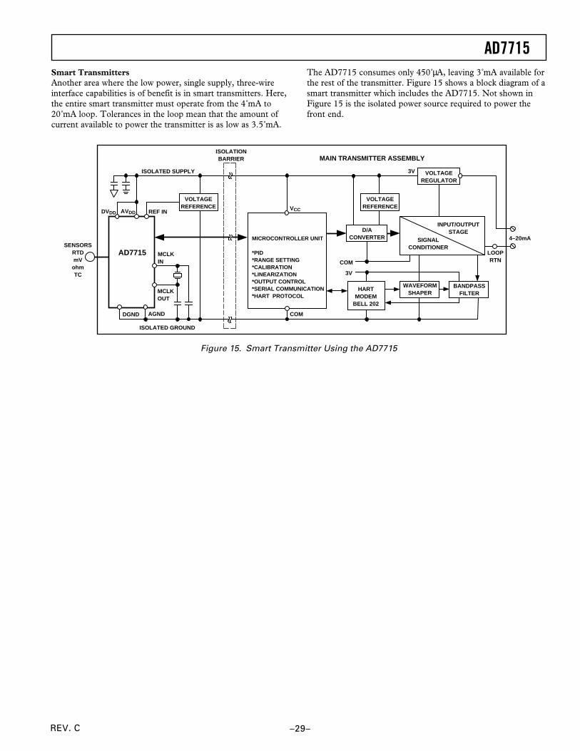
AD7715
–29–REV. C
Smart TransmittersAnother area where the low power, single supply, three-wireinterface capabilities is of benefit is in smart transmitters. Here,the entire smart transmitter must operate from the 4 mA to20 mA loop. Tolerances in the loop mean that the amount ofcurrent available to power the transmitter is as low as 3.5 mA.
The AD7715 consumes only 450 µA, leaving 3 mA available forthe rest of the transmitter. Figure 15 shows a block diagram of asmart transmitter which includes the AD7715. Not shown inFigure 15 is the isolated power source required to power thefront end.
INPUT/OUTPUTSTAGE
SIGNALCONDITIONER
MICROCONTROLLER UNIT
*PID*RANGE SETTING*CALIBRATION*LINEARIZATION*OUTPUT CONTROL*SERIAL COMMUNICATION*HART PROTOCOL
VOLTAGEREFERENCE
MCLKOUT
AD7715
ISOLATED SUPPLY
ISOLATIONBARRIER
SENSORSRTDmVohmTC
LOOPRTN
MCLKIN COM
3V
4–20mA
DVDD AVDD REF IN
AGND DGND
ISOLATED GROUND
COM
VCC
3V
MAIN TRANSMITTER ASSEMBLY
BANDPASSFILTER
WAVEFORMSHAPER
HARTMODEM
BELL 202
D/ACONVERTER
VOLTAGEREFERENCE
VOLTAGEREGULATOR
Figure 15. Smart Transmitter Using the AD7715
REV. C
AD7715
–30–
PAGE INDEXTopic PageFEATURES . . . . . . . . . . . . . . . . . . . . . . . . . . . . . . . . . . . . . 1GENERAL DESCRIPTION . . . . . . . . . . . . . . . . . . . . . . . . . 1PRODUCT HIGHLIGHTS . . . . . . . . . . . . . . . . . . . . . . . . . 1AD7715-5 SPECIFICATIONS . . . . . . . . . . . . . . . . . . . . . . . 2AD7715-3 SPECIFICATIONS . . . . . . . . . . . . . . . . . . . . . . . 3SPECIFICATIONS . . . . . . . . . . . . . . . . . . . . . . . . . . . . . . . 4TIMING CHARACTERISTICS . . . . . . . . . . . . . . . . . . . . . 5ABSOLUTE MAXIMUM RATINGS . . . . . . . . . . . . . . . . . 6ORDERING GUIDE . . . . . . . . . . . . . . . . . . . . . . . . . . . . . . 6PIN CONFIGURATION . . . . . . . . . . . . . . . . . . . . . . . . . . . 6PIN FUNCTION DESCRIPTION . . . . . . . . . . . . . . . . . . . 7TERMINOLOGY . . . . . . . . . . . . . . . . . . . . . . . . . . . . . . . . . 8ON-CHIP REGISTERS . . . . . . . . . . . . . . . . . . . . . . . . . . . . 8
Communications Register . . . . . . . . . . . . . . . . . . . . . . . . . 9Setup Register . . . . . . . . . . . . . . . . . . . . . . . . . . . . . . . . . 10Test Register . . . . . . . . . . . . . . . . . . . . . . . . . . . . . . . . . . 11Data Register . . . . . . . . . . . . . . . . . . . . . . . . . . . . . . . . . . 11
OUTPUT NOISE . . . . . . . . . . . . . . . . . . . . . . . . . . . . . . . . 11AD7715-5 . . . . . . . . . . . . . . . . . . . . . . . . . . . . . . . . . . . . 12AD7715-3 . . . . . . . . . . . . . . . . . . . . . . . . . . . . . . . . . . . . 13
CALIBRATION SEQUENCES . . . . . . . . . . . . . . . . . . . . . 14CIRCUIT DESCRIPTION . . . . . . . . . . . . . . . . . . . . . . . . 14ANALOG INPUT . . . . . . . . . . . . . . . . . . . . . . . . . . . . . . . . 15
Analog Input Ranges . . . . . . . . . . . . . . . . . . . . . . . . . . . . 15Input Sample Rate . . . . . . . . . . . . . . . . . . . . . . . . . . . . . . 15Bipolar/Unipolar Inputs . . . . . . . . . . . . . . . . . . . . . . . . . . 15
REFERENCE INPUT . . . . . . . . . . . . . . . . . . . . . . . . . . . . 16DIGITAL FILTERING . . . . . . . . . . . . . . . . . . . . . . . . . . . 16
Filter Characteristics . . . . . . . . . . . . . . . . . . . . . . . . . . . . 16Post-Filtering . . . . . . . . . . . . . . . . . . . . . . . . . . . . . . . . . . 17
ANALOG FILTERING . . . . . . . . . . . . . . . . . . . . . . . . . . . 17CALIBRATION . . . . . . . . . . . . . . . . . . . . . . . . . . . . . . . . . 17
Self-Calibration . . . . . . . . . . . . . . . . . . . . . . . . . . . . . . . . 18System Calibration . . . . . . . . . . . . . . . . . . . . . . . . . . . . . . 18Span and Offset Limits . . . . . . . . . . . . . . . . . . . . . . . . . . 18Power-Up and Calibration . . . . . . . . . . . . . . . . . . . . . . . . 19
USING THE AD7715 . . . . . . . . . . . . . . . . . . . . . . . . . . . . 19Clocking and Oscillator Circuit . . . . . . . . . . . . . . . . . . . . 19System Synchronization . . . . . . . . . . . . . . . . . . . . . . . . . . 20Reset Input . . . . . . . . . . . . . . . . . . . . . . . . . . . . . . . . . . . 20Standby Mode . . . . . . . . . . . . . . . . . . . . . . . . . . . . . . . . . 20Accuracy . . . . . . . . . . . . . . . . . . . . . . . . . . . . . . . . . . . . . 20Drift Considerations . . . . . . . . . . . . . . . . . . . . . . . . . . . . 20
POWER SUPPLIES . . . . . . . . . . . . . . . . . . . . . . . . . . . . . . 21Supply Current . . . . . . . . . . . . . . . . . . . . . . . . . . . . . . . . 21Grounding and Layout . . . . . . . . . . . . . . . . . . . . . . . . . . . 21Evaluating the AD7715 Performance . . . . . . . . . . . . . . . . 21
DIGITAL INTERFACE . . . . . . . . . . . . . . . . . . . . . . . . . . . 22CONFIGURING THE AD7715 . . . . . . . . . . . . . . . . . . . . . 23MICROCOMPUTER/MICROPROCESSOR
INTERFACING . . . . . . . . . . . . . . . . . . . . . . . . . . . . . . . 24AD7715 to 68HC11 Interface . . . . . . . . . . . . . . . . . . . . . 24AD7715 to 8XC51 Interface . . . . . . . . . . . . . . . . . . . . . . 25AD7715 to ADSP-2103/ADSP-2105 Interface . . . . . . . . 25
Topic PageCODE FOR SETTING UP AD7715 . . . . . . . . . . . . . . . . . 25APPLICATIONS . . . . . . . . . . . . . . . . . . . . . . . . . . . . . . . . 27
Pressure Measurement . . . . . . . . . . . . . . . . . . . . . . . . . . . 27Temperature Measurement . . . . . . . . . . . . . . . . . . . . . . . 28Smart Transmitters . . . . . . . . . . . . . . . . . . . . . . . . . . . . . 29
INDEX . . . . . . . . . . . . . . . . . . . . . . . . . . . . . . . . . . . . . . . . 30OUTLINE DIMENSIONS . . . . . . . . . . . . . . . . . . . . . . . . . 31
TABLE INDEXTable TitleTable I Communications Register . . . . . . . . . . . . . . . . . . 9
Table II Register Selection . . . . . . . . . . . . . . . . . . . . . . . . 9
Table III Setup Register . . . . . . . . . . . . . . . . . . . . . . . . . . 10
Table IV Output Update Rates . . . . . . . . . . . . . . . . . . . . 11
Table V Output RMS Noise vs. Gain and Output UpdateRate for AD7715-5 (Unbuffered Mode) . . . . . . 12
Table VI Peak-to-Peak Resolution vs. Gain and OutputUpdate Rate for AD7715-5 (Unbuffered Mode) . . 12
Table VII Output RMS Noise vs. Gain and Output UpdateRate for AD7715-5 (Buffered Mode) . . . . . . . . . 12
Table VIII Peak-to-Peak Resolution vs. Gain and OutputUpdate Rate for AD7715-5 (Buffered Mode) . . 12
Table IX Output RMS Noise vs. Gain and Output UpdateRate for AD7715-3 (Unbuffered Mode) . . . . . . 13
Table X Peak-to-Peak Resolution vs. Gain and OutputUpdate Rate for AD7715-3 (Unbuffered Mode) . . 13
Table XI Output RMS Noise vs. Gain and Output UpdateRate for AD7715-5 (Buffered Mode) . . . . . . . . 13
Table XII Peak-to-Peak Resolution vs. Gain and OutputUpdate Rate for AD7715-3 (Buffered Mode) . . 13
Table XIII Calibration Sequences . . . . . . . . . . . . . . . . . . . . 14
Table XIV External R, C Combination for No 16-BitGain Error . . . . . . . . . . . . . . . . . . . . . . . . . . . . . 15
Table XV Input Sampling Frequency vs. Gain . . . . . . . . . 15
Table XVI C Code for Interfacing AD7715 to 68HC11 . . . 26
AD7715
–31–REV. C
OUTLINE DIMENSIONSDimensions shown in inches and (mm).
16-Lead Plastic DIP(N-16)
16
1 8
9
0.840 (21.33)
0.745 (18.93)
0.280 (7.11)0.240 (6.10)
PIN 1
SEATINGPLANE
0.022 (0.558)0.014 (0.356)
0.060 (1.52)0.015 (0.38)0.210 (5.33)
MAX 0.130(3.30)MIN
0.070 (1.77)0.045 (1.15)
0.100(2.54)BSC
0.160 (4.06) 0.115 (2.93)
0.325 (8.25)
0.300 (7.62)
0.015 (0.381)0.008 (0.204)
0.195 (4.95)0.115 (2.93)
16-Lead SOIC(R-16)
16 9
81
0.4133 (10.50)
0.3977 (10.00)0.
4193
(10
.65)
0.39
37 (
10.0
0)
0.29
92 (
7.60
)
0.29
14 (
7.40
)
PIN 1
SEATINGPLANE
0.0118 (0.30)
0.0040 (0.10)
0.0192 (0.49)
0.0138 (0.35)
0.1043 (2.65)
0.0926 (2.35)
0.0500(1.27)BSC
0.0125 (0.32)
0.0091 (0.23)
0.0500 (1.27)
0.0157 (0.40)80
0.0291 (0.74)
0.0098 (0.25)3 45°
16-Lead TSSOP(RU-16)
16 9
81
0.201 (5.10)0.193 (4.90)
0.25
6 (6
.50)
0.24
6 (6
.25)
0.17
7 (4
.50)
0.16
9 (4
.30)
PIN 1
SEATINGPLANE
0.006 (0.15)0.002 (0.05)
0.0118 (0.30)0.0075 (0.19)
0.0256(0.65)BSC
0.0433(1.10)MAX
0.0079 (0.20)0.0035 (0.090)
0.028 (0.70)0.020 (0.50)
8°0°
C20
16b
–2.5
–2/0
0 (r
ev. C
)P
RIN
TE
D IN
U.S
.A.
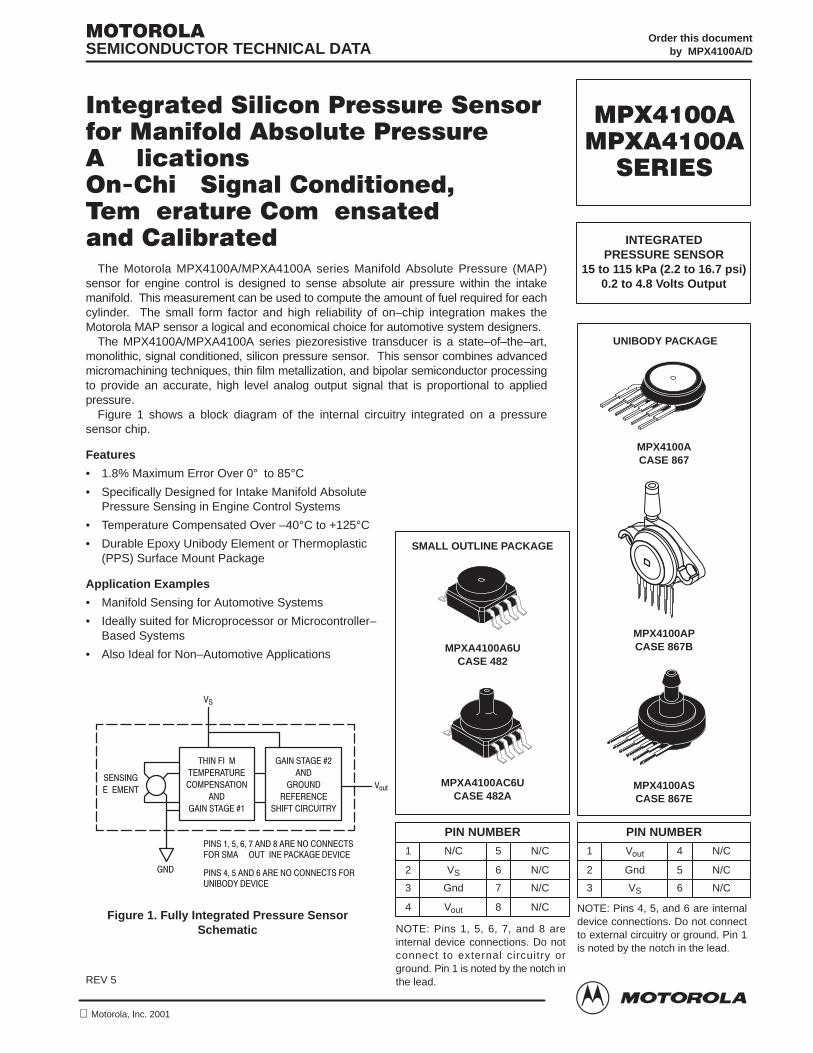
1Motorola Sensor Device Data
#!# !""$! "!! "$# !""$! #" # !#$! "# !#
The Motorola MPX4100A/MPXA4100A series Manifold Absolute Pressure (MAP)sensor for engine control is designed to sense absolute air pressure within the intakemanifold. This measurement can be used to compute the amount of fuel required for eachcylinder. The small form factor and high reliability of on–chip integration makes theMotorola MAP sensor a logical and economical choice for automotive system designers.
The MPX4100A/MPXA4100A series piezoresistive transducer is a state–of–the–art,monolithic, signal conditioned, silicon pressure sensor. This sensor combines advancedmicromachining techniques, thin film metallization, and bipolar semiconductor processingto provide an accurate, high level analog output signal that is proportional to appliedpressure.
Figure 1 shows a block diagram of the internal circuitry integrated on a pressuresensor chip.
Features
• 1.8% Maximum Error Over 0° to 85°C• Specifically Designed for Intake Manifold Absolute
Pressure Sensing in Engine Control Systems
• Temperature Compensated Over –40°C to +125°C• Durable Epoxy Unibody Element or Thermoplastic
(PPS) Surface Mount Package
Application Examples
• Manifold Sensing for Automotive Systems
• Ideally suited for Microprocessor or Microcontroller–Based Systems
• Also Ideal for Non–Automotive Applications
*'
'"'"
!"(*9>=
"
(" !
(!$&()&
#!$"'(#"
"
" '(
" '(
"
&#)"
&&"
'( &)(&-
$"' " & "# #""('#& '! #)( " $ *
$"' " & "# #""(' #&)"#- *
Figure 1. Fully Integrated Pressure SensorSchematic
Order this documentby MPX4100A/D
SEMICONDUCTOR TECHNICAL DATA
Motorola, Inc. 2001
INTEGRATEDPRESSURE SENSOR
15 to 115 kPa (2.2 to 16.7 psi)0.2 to 4.8 Volts Output
PIN NUMBER
NOTE: Pins 4, 5, and 6 are internaldevice connections. Do not connectto external circuitry or ground. Pin 1is noted by the notch in the lead.
MPX4100ACASE 867
MPX4100APCASE 867B
1
2
3
Vout
Gnd
VS
4
5
6
N/C
N/C
N/C
UNIBODY PACKAGE
PIN NUMBER
NOTE: Pins 1, 5, 6, 7, and 8 areinternal device connections. Do notconnect to external circuitry orground. Pin 1 is noted by the notch inthe lead.
1
2
3
N/C
VS
Gnd
5
6
7
N/C
N/C
N/C
MPXA4100A6UCASE 482
MPXA4100AC6UCASE 482A
4 Vout 8 N/C
SMALL OUTLINE PACKAGE
MPX4100ASCASE 867E
REV 5
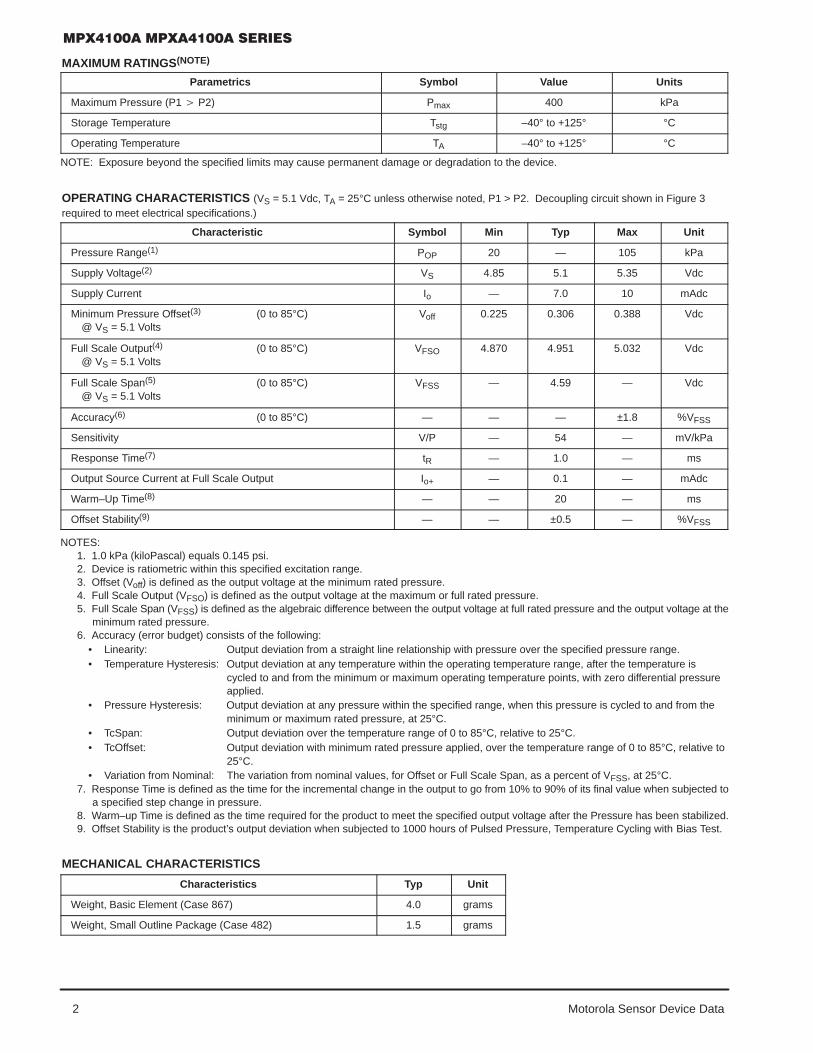
2 Motorola Sensor Device Data
MAXIMUM RATINGS(NOTE)
Parametrics Symbol Value Units
Maximum Pressure (P1 P2) Pmax 400 kPa
Storage Temperature Tstg –40° to +125° °C
Operating Temperature TA –40° to +125° °C
NOTE: Exposure beyond the specified limits may cause permanent damage or degradation to the device.
OPERATING CHARACTERISTICS (VS = 5.1 Vdc, TA = 25°C unless otherwise noted, P1 > P2. Decoupling circuit shown in Figure 3required to meet electrical specifications.)
Characteristic Symbol Min Typ Max Unit
Pressure Range(1) POP 20 — 105 kPa
Supply Voltage(2) VS 4.85 5.1 5.35 Vdc
Supply Current Io — 7.0 10 mAdc
Minimum Pressure Offset(3) (0 to 85°C)@ VS = 5.1 Volts
Voff 0.225 0.306 0.388 Vdc
Full Scale Output(4) (0 to 85°C)@ VS = 5.1 Volts
VFSO 4.870 4.951 5.032 Vdc
Full Scale Span(5) (0 to 85°C)@ VS = 5.1 Volts
VFSS — 4.59 — Vdc
Accuracy(6) (0 to 85°C) — — — ±1.8 %VFSS
Sensitivity V/P — 54 — mV/kPa
Response Time(7) tR — 1.0 — ms
Output Source Current at Full Scale Output Io+ — 0.1 — mAdc
Warm–Up Time(8) — — 20 — ms
Offset Stability(9) — — ±0.5 — %VFSS
NOTES:1. 1.0 kPa (kiloPascal) equals 0.145 psi.2. Device is ratiometric within this specified excitation range.3. Offset (Voff) is defined as the output voltage at the minimum rated pressure.4. Full Scale Output (VFSO) is defined as the output voltage at the maximum or full rated pressure.5. Full Scale Span (VFSS) is defined as the algebraic difference between the output voltage at full rated pressure and the output voltage at the
minimum rated pressure.6. Accuracy (error budget) consists of the following:
• Linearity: Output deviation from a straight line relationship with pressure over the specified pressure range.• Temperature Hysteresis: Output deviation at any temperature within the operating temperature range, after the temperature is
cycled to and from the minimum or maximum operating temperature points, with zero differential pressureapplied.
• Pressure Hysteresis: Output deviation at any pressure within the specified range, when this pressure is cycled to and from theminimum or maximum rated pressure, at 25°C.
• TcSpan: Output deviation over the temperature range of 0 to 85°C, relative to 25°C.• TcOffset: Output deviation with minimum rated pressure applied, over the temperature range of 0 to 85°C, relative to
25°C.• Variation from Nominal: The variation from nominal values, for Offset or Full Scale Span, as a percent of VFSS, at 25°C.
7. Response Time is defined as the time for the incremental change in the output to go from 10% to 90% of its final value when subjected toa specified step change in pressure.
8. Warm–up Time is defined as the time required for the product to meet the specified output voltage after the Pressure has been stabilized.9. Offset Stability is the product’s output deviation when subjected to 1000 hours of Pulsed Pressure, Temperature Cycling with Bias Test.
MECHANICAL CHARACTERISTICS
Characteristics Typ Unit
Weight, Basic Element (Case 867) 4.0 grams
Weight, Small Outline Package (Case 482) 1.5 grams
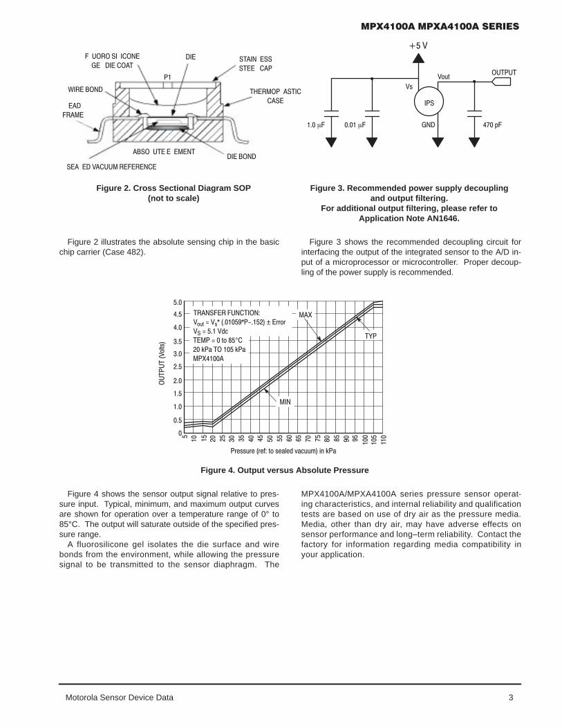
3Motorola Sensor Device Data
Figure 2. Cross Sectional Diagram SOP(not to scale)
Figure 3. Recommended power supply decouplingand output filtering.
For additional output filtering, please refer toApplication Note AN1646.
$'
:
#)($)(
*<
*
"
*9>=
+& #"
'(" ''
'( $
(&!#$ '(
'
#"
' *))! &&"
$
)#&# ' #"
#(
&!
'# )( !"(
Figure 2 illustrates the absolute sensing chip in the basicchip carrier (Case 482).
Figure 3 shows the recommended decoupling circuit forinterfacing the output of the integrated sensor to the A/D in-put of a microprocessor or microcontroller. Proper decoup-ling of the power supply is recommended.
#)($)(*96=<
$;1<<>;1 ;12 =9 <1.610 ?./>>7 48 5$.
(-$
!,
!"
(!$ =9 ° 5$. (# 5$.
!$,
(&"'& )"(#"
*9>= *< $ ± ;;9;*' *0/
Figure 4. Output versus Absolute Pressure
Figure 4 shows the sensor output signal relative to pres-sure input. Typical, minimum, and maximum output curvesare shown for operation over a temperature range of 0° to85°C. The output will saturate outside of the specified pres-sure range.
A fluorosilicone gel isolates the die surface and wirebonds from the environment, while allowing the pressuresignal to be transmitted to the sensor diaphragm. The
MPX4100A/MPXA4100A series pressure sensor operat-ing characteristics, and internal reliability and qualificationtests are based on use of dry air as the pressure media.Media, other than dry air, may have adverse effects onsensor performance and long–term reliability. Contact thefactory for information regarding media compatibility inyour application.
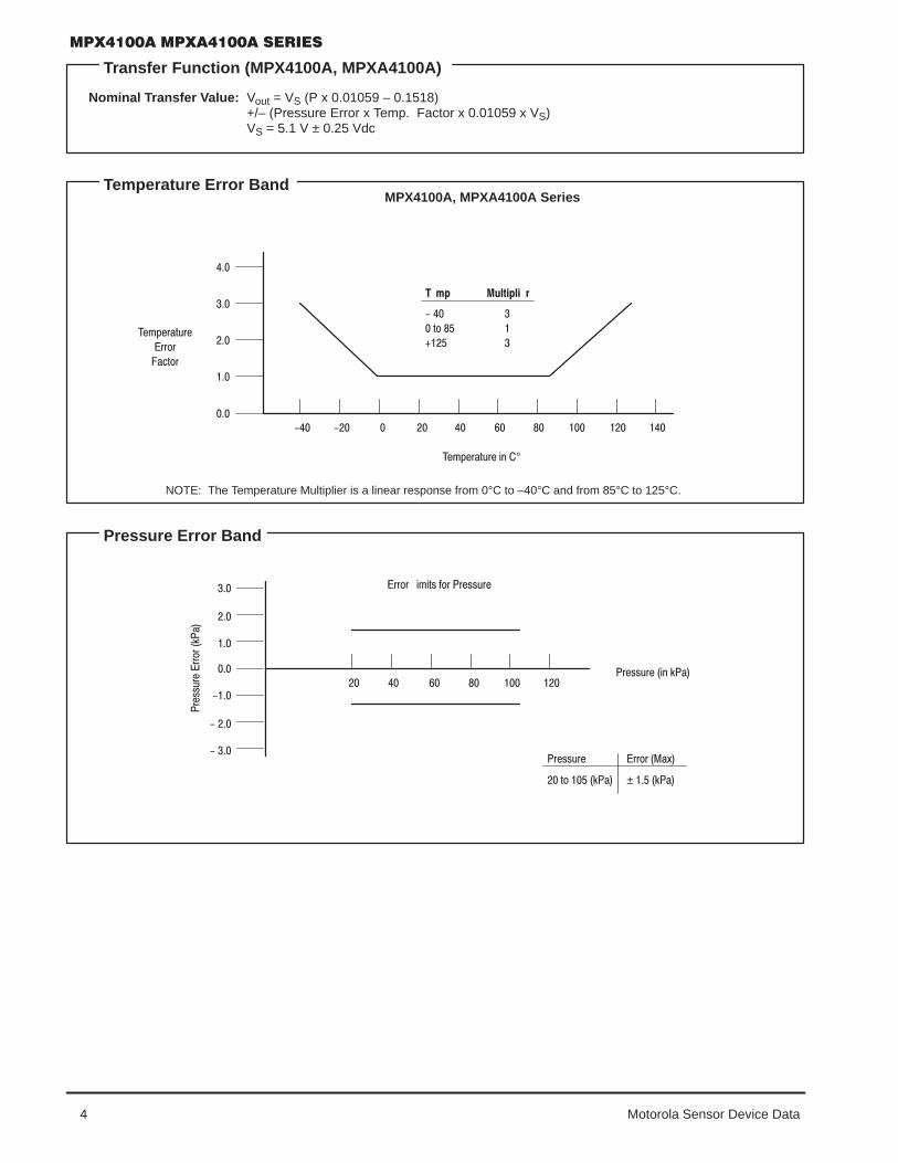
4 Motorola Sensor Device Data
Transfer Function (MPX4100A, MPXA4100A)
Nominal Transfer Value: Vout = VS (P x 0.01059 – 0.1518)+/– (Pressure Error x Temp. Factor x 0.01059 x VS)VS = 5.1 V ± 0.25 Vdc
Temperature Error BandMPX4100A, MPXA4100A Series
#$ '"&!$"! %
=9
(17:1;.=>;1 48 °
(17:1;.=>;1
;;9;
./=9;
NOTE: The Temperature Multiplier is a linear response from 0°C to –40°C and from 85°C to 125°C.
Pressure Error Band
;;9; 474=< 29; $;1<<>;1
A
A
$;1<<>;1 48 5$.
$;1<<>;1;;9;5$
.
$;1<<>;1 ;;9; !.@
=9 5$. ±A 5$.
5Motorola Sensor Device Data
PRESSURE (P1)/VACUUM (P2) SIDE IDENTIFICATION TABLE
Motorola designates the two sides of the pressure sensoras the Pressure (P1) side and the Vacuum (P2) side. ThePressure (P1) side is the side containing fluorosilicone gelwhich protects the die from harsh media. The Motorola MPX
pressure sensor is designed to operate with positive differen-tial pressure applied, P1 > P2.
The Pressure (P1) side may be identified by using the tablebelow:
Part Number Case TypePressure (P1)Side Identifier
MPX4100A 867 Stainless Steel Cap
MPX4100AP 867B Side with Port Marking
MPX4100AS 867E Side with Port Attached
MPXA4100A6U/T1 482 Stainless Steel Cap
MPXA4100AC6U 482A Side with Port Attached
ORDERING INFORMATION — UNIBODY PACKAGE
MPX Series
Device Type Options Case Type Order Number Device Marking
Basic Element Absolute, Element Only 867 MPX4100A MPX4100A
Ported Elements Absolute, Ported 867B MPX4100AP MPX4100AP
Absolute, Stove Pipe Port 867E MPX4100AS MPX4100A
ORDERING INFORMATION — SMALL OUTLINE PACKAGE
Device Type Options Case No. MPX Series Order No. Packing Options Marking
Basic Element Absolute, Element Only 482 MPXA4100A6U Rails MPXA4100A
Absolute, Element Only 482 MPXA4100A6T1 Tape and Reel MPXA4100A
Ported Element Absolute, Axial Port 482A MPXA4100AC6U Rails MPXA4100A
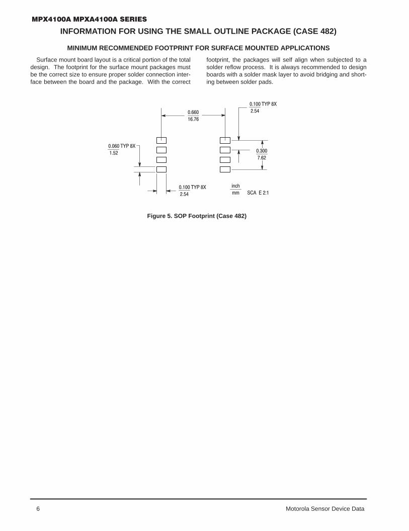
6 Motorola Sensor Device Data
INFORMATION FOR USING THE SMALL OUTLINE PACKAGE (CASE 482)
MINIMUM RECOMMENDED FOOTPRINT FOR SURFACE MOUNTED APPLICATIONS
Surface mount board layout is a critical portion of the totaldesign. The footprint for the surface mount packages mustbe the correct size to ensure proper solder connection inter-face between the board and the package. With the correct
footprint, the packages will self align when subjected to asolder reflow process. It is always recommended to designboards with a solder mask layer to avoid bridging and short-ing between solder pads.
(-$,
(-$,
(-$,
48/3
77 '
Figure 5. SOP Footprint (Case 482)
7Motorola Sensor Device Data
UNIBODY PACKAGE DIMENSIONS
BASIC ELEMENT
CASE 867–08ISSUE N
'(- $" *#)(
&#)" * * * *,
PIN 1
FG
NL
RC
B
M
JS
"#(' !"'#"" " (# &"" $& "'
-! #"(&# " !"'#" " !"'#" ' " )'* # ( !#
'(#$ &" !# '(#$ &" "#( (# , –A–
6 PLD
–T–
!! (
' '
"#! "#!
'(- $" #$"
&#)" *#)( *')$$ - *#)( #$"
'(- $" #$"
&#)" *#)( *')$$ - *#)( #$"
POSITIVE PRESSURE(P1)
PRESSURE SIDE PORTED (AP, GP)
CASE 867B–04ISSUE F
'(- $" *#)(
&#)" * * * *,
R
N
C
J
PIN 1
!%! (
B
6X DGF
S
K
V
'$! % '(
LUA
"#(' !"'#"' & " ! !(&' !"'#"' " (# &"' $& '!
-!
'
'
T
P
P
Q
Q
8 Motorola Sensor Device Data
UNIBODY PACKAGE DIMENSIONS—CONTINUED
PRESSURE SIDE PORTED (AS, GS)
CASE 867E–03ISSUE D
"#(' !"'#"" " (# &"" $& "'
-! #"(&# " !"'#" "
'(- $" *#)(
&#)" * * * *,
A
C
K
N E
–B–
PORT #1POSITIVE
PRESSURE
J
–T–
S
GF
D 6 PL
PIN 1
!! (
' '
V
(P1)
9Motorola Sensor Device Data
SMALL OUTLINE PACKAGE DIMENSIONS
CASE 482–01ISSUE O
' '
"#(' !"'#"" " (# &"" $& "'
-! #"(&# " !"'#" " !"'#" " # "#( " ) !#
$&#(&)'#" !,!)! !# $&#(&)'#" *&( ')&' (-$ &(
S
D
G
8 PL
N
'! '(
–A–
–B–
C
M
J
KPIN 1 IDENTIFIER
H
–T–
CASE 482A–01ISSUE A
' '
"#(' !"'#"" " (# &"" $& "'
-! #"(&# " !"'#" " !"'#" " # "#( " ) !#
$&#(&)'#" !,!)! !# $&#(&)'#" *&( ')&' (-$ &(
S
D
G
8 PL
'! '(
–A–
–B–
C
M
J
KPIN 1 IDENTIFIER
H
–T–
N
V
W

10 Motorola Sensor Device Data
Motorola reserves the right to make changes without further notice to any products herein. Motorola makes no warranty, representation orguarantee regarding the suitability of its products for any particular purpose, nor does Motorola assume any liability arising out of theapplication or use of any product or circuit, and specifically disclaims any and all liability, including without limitation consequential or incidentaldamages. “Typical” parameters which may be provided in Motorola data sheets and/or specifications can and do vary in different applicationsand actual performance may vary over time. All operating parameters, including “Typicals” must be validated for each customer applicationby customer’s technical experts. Motorola does not convey any license under its patent rights nor the rights of others. Motorola products arenot designed, intended, or authorized for use as components in systems intended for surgical implant into the body, or other applicationsintended to support or sustain life, or for any other application in which the failure of the Motorola product could create a situation wherepersonal injury or death may occur. Should Buyer purchase or use Motorola products for any such unintended or unauthorized application,Buyer shall indemnify and hold Motorola and its officers, employees, subsidiaries, affiliates, and distributors harmless against all claims, costs,damages, and expenses, and reasonable attorney fees arising out of, directly or indirectly, any claim of personal injury or death associatedwith such unintended or unauthorized use, even if such claim alleges that Motorola was negligent regarding the design or manufacture of thepart. Motorola and are registered trademarks of Motorola, Inc. Motorola, Inc. is an Equal Opportunity/Affirmative Action Employer.
How to reach us:USA/EUROPE/Locations Not Listed : Motorola Literature Distribution; JAPAN : Motorola Japan Ltd.; SPS, Technical Information Center, 3–20–1,P.O. Box 5405, Denver, Colorado 80217. 1–303–675–2140 or 1–800–441–2447 Minami–Azabu. Minato–ku, Tokyo 106–8573 Japan. 81–3–3440–3569
Technical Information Center: 1–800–521–6274 ASIA/PACIFIC : Motorola Semiconductors H.K. Ltd.; Silicon Harbour Centre,2, Dai King Street, Tai Po Industrial Estate, Tai Po, N.T., Hong Kong. 852–26668334
HOME PAGE: http://www.motorola.com/semiconductors/
MPX4100A/D◊
167
HD44780U (LCD-II)
(Dot Matrix Liquid Crystal Display Controller/Driver)
Description
The HD44780U dot-matrix liquid crystal display controller and driver LSI displays alphanumerics,Japanese kana characters, and symbols. It can be configured to drive a dot-matrix liquid crystal displayunder the control of a 4- or 8-bit microprocessor. Since all the functions such as display RAM, charactergenerator, and liquid crystal driver, required for driving a dot-matrix liquid crystal display are internallyprovided on one chip, a minimal system can be interfaced with this controller/driver.
A single HD44780U can display up to one 8-character line or two 8-character lines.
The HD44780U has pin function compatibility with the HD44780S which allows the user to easilyreplace an LCD-II with an HD44780U. The HD44780U character generator ROM is extended to generate208 5 × 8 dot character fonts and 32 5 × 10 dot character fonts for a total of 240 different character fonts.
The low power supply (2.7V to 5.5V) of the HD44780U is suitable for any portable battery-drivenproduct requiring low power dissipation.
Features
• 5 × 8 and 5 × 10 dot matrix possible
• Low power operation support:
2.7 to 5.5V
• Wide range of liquid crystal display driver power
3.0 to 11V
• Liquid crystal drive waveform
A (One line frequency AC waveform)
• Correspond to high speed MPU bus interface
2 MHz (when VCC = 5V)
• 4-bit or 8-bit MPU interface enabled
• 80 × 8-bit display RAM (80 characters max.)
• 9,920-bit character generator ROM for a total of 240 character fonts
208 character fonts (5 × 8 dot)
32 character fonts (5 × 10 dot)
HD44780U
168
• 64 × 8-bit character generator RAM
8 character fonts (5 × 8 dot)
4 character fonts (5 × 10 dot)
• 16-common × 40-segment liquid crystal display driver
• Programmable duty cycles
1/8 for one line of 5 × 8 dots with cursor
1/11 for one line of 5 × 10 dots with cursor
1/16 for two lines of 5 × 8 dots with cursor
• Wide range of instruction functions:
Display clear, cursor home, display on/off, cursor on/off, display character blink, cursor shift,display shift
• Pin function compatibility with HD44780S
• Automatic reset circuit that initializes the controller/driver after power on
• Internal oscillator with external resistors
• Low power consumption
Ordering Information
Type No. Package CGROM
HD44780UA00FSHCD44780UA00HD44780UA00TF
FP-80BChipTFP-80F
Japanese standard font
HD44780UA02FSHCD44780UA02HD44780UA02TF
FP-80BChipTFP-80F
European standard font
HD44780UBxxFSHCD44780UBxxHD44780UBxxTF
FP-80BChipTFP-80F
Custom font
Note: xx: ROM code No.
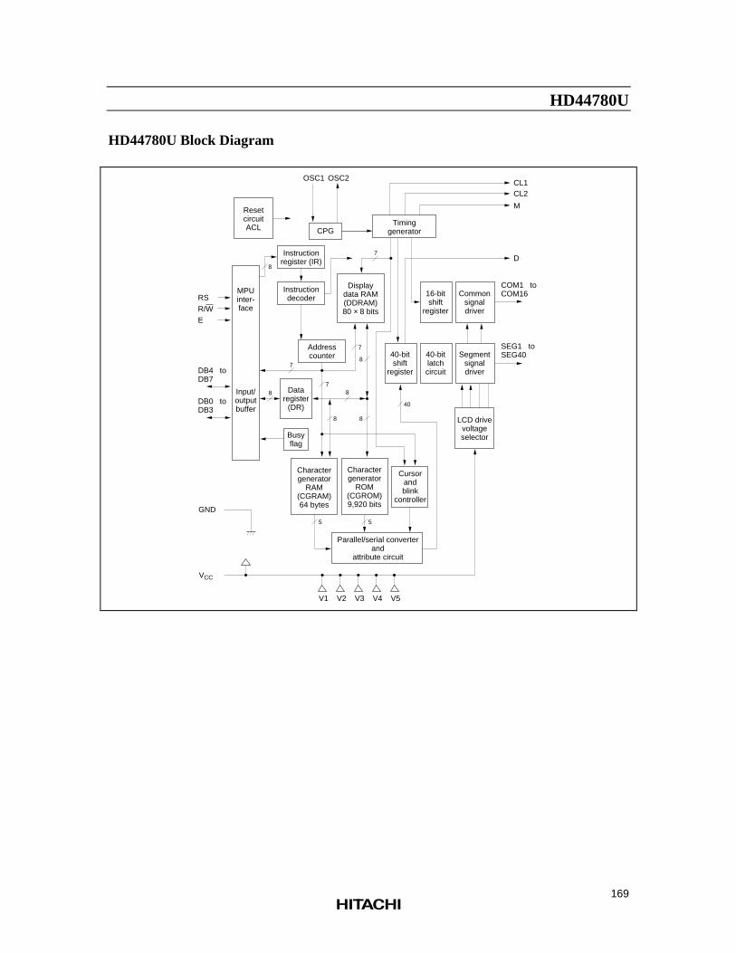
HD44780U
169
HD44780U Block Diagram
Displaydata RAM(DDRAM)80 × 8 bits
Charactergenerator
ROM(CGROM)9,920 bits
Charactergenerator
RAM(CGRAM)64 bytes
Instructionregister (IR)
Timinggenerator
Commonsignaldriver
16-bitshift
register
Segmentsignaldriver
40-bitlatchcircuit
40-bitshift
register
Parallel/serial converterand
attribute circuit
LCD drivevoltageselector
Addresscounter
MPUinter-face
Input/outputbuffer
Dataregister
(DR)
Cursorandblink
controller
CPG
CL1CL2
M
D
RSR/W
DB4 to DB7
E
Instructiondecoder
OSC1 OSC2
COM1 toCOM16
SEG1 toSEG40
8
8 8
7
40
55
7
8
7
8
7
VCC
GND
V1 V2 V3 V4 V5
DB0 to DB3
ResetcircuitACL
8
Busyflag
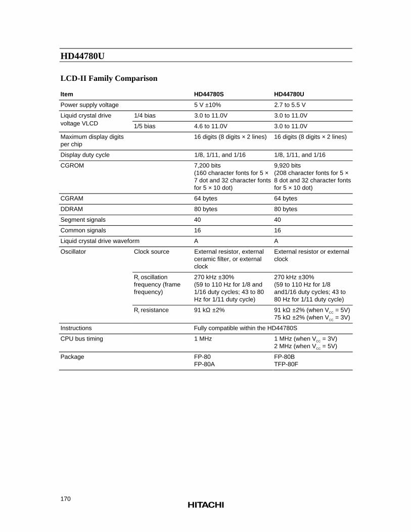
HD44780U
170
LCD-II Family Comparison
Item HD44780S HD44780U
Power supply voltage 5 V ±10% 2.7 to 5.5 V
Liquid crystal drive 1/4 bias 3.0 to 11.0V 3.0 to 11.0Vvoltage VLCD 1/5 bias 4.6 to 11.0V 3.0 to 11.0V
Maximum display digitsper chip
16 digits (8 digits × 2 lines) 16 digits (8 digits × 2 lines)
Display duty cycle 1/8, 1/11, and 1/16 1/8, 1/11, and 1/16
CGROM 7,200 bits(160 character fonts for 5 ×7 dot and 32 character fontsfor 5 × 10 dot)
9,920 bits(208 character fonts for 5 ×8 dot and 32 character fontsfor 5 × 10 dot)
CGRAM 64 bytes 64 bytes
DDRAM 80 bytes 80 bytes
Segment signals 40 40
Common signals 16 16
Liquid crystal drive waveform A A
Oscillator Clock source External resistor, externalceramic filter, or externalclock
External resistor or externalclock
Rf oscillationfrequency (framefrequency)
270 kHz ±30%(59 to 110 Hz for 1/8 and1/16 duty cycles; 43 to 80Hz for 1/11 duty cycle)
270 kHz ±30%(59 to 110 Hz for 1/8and1/16 duty cycles; 43 to80 Hz for 1/11 duty cycle)
Rf resistance 91 kΩ ±2% 91 kΩ ±2% (when VCC = 5V)75 kΩ ±2% (when VCC = 3V)
Instructions Fully compatible within the HD44780S
CPU bus timing 1 MHz 1 MHz (when VCC = 3V)2 MHz (when VCC = 5V)
Package FP-80FP-80A
FP-80BTFP-80F
HD44780U
171
HD44780U Pin Arrangement (FP-80B)
1
2
3
4
5
6
7
8
9
10
11
12
13
14
15
16
17
18
19
20
21
22
23
24
80
79
78
77
76
75
74
73
72
71
70
69
68
67
66
65
64
63
62
61
60
59
58
57
56
55
54
53
52
51
50
49
48
47
46
45
44
43
42
41
25
26
27
28
29
30
31
32
33
34
35
36
37
38
39
40
FP-80B (Top view)
SEG39SEG40COM16 COM15COM14COM13COM12COM11COM10COM9COM8COM7COM6COM5COM4COM3COM2COM1DB7DB6DB5DB4DB3DB2
SEG22SEG21 SEG20SEG19SEG18SEG17SEG16SEG15SEG14SEG13SEG12SEG11SEG10SEG9SEG8SEG7SEG6SEG5SEG4SEG3SEG2SEG1GND
OSC1
SE
G23
SE
G24
SE
G25
SE
G26
SE
G27
SE
G28
SE
G29
SE
G30
SE
G31
SE
G32
SE
G33
SE
G34
SE
G35
SE
G36
SE
G37
OS
C2
V1
V2
V3
V4
V5
CL1
C
L2
VC
C
M
D
RS
R
/W
ED
B0
DB
1S
EG
38
HD44780U
172
HD44780U Pin Arrangement (TFP-80F)
1
2
3
4
5
6
7
8
9
10
11
12
13
14
15
16
17
18
19
20
80
79
78
77
76
75
74
73
72
71
70
69
68
67
66
65
64
63
62
61
60
59
58
57
56
55
54
53
52
51
50
49
48
47
46
45
44
43
42
41
21
22
23
24
25
26
27
28
29
30
31
32
33
34
35
36
37
38
39
40
TFP-80F (Top view)
COM16 COM15 COM14 COM13 COM12 COM11 COM10 COM9 COM8 COM7 COM6 COM5 COM4 COM3 COM2 COM1 DB7 DB6 DB5 DB4
SEG20 SEG19 SEG18 SEG17 SEG16 SEG15 SEG14 SEG13 SEG12 SEG11 SEG10 SEG9 SEG8 SEG7 SEG6 SEG5 SEG4 SEG3 SEG2 SEG1
SE
G21
S
EG
22
SE
G23
S
EG
24
SE
G25
S
EG
26
SE
G27
S
EG
28
SE
G29
S
EG
30
SE
G31
S
EG
32
SE
G33
S
EG
34
SE
G35
S
EG
36
SE
G37
S
EG
38
SE
G39
S
EG
40
GN
D
OS
C1
OS
C2
V1
V2
V3
V4
V5
CL1
C
L2
VC
C
M
D
RS
R
/W
E
DB
0 D
B1
DB
2 D
B3
HD44780U
173
HD44780U Pad Arrangement
HD44780U
Type code
23
X
Y
42
2 1 80 63
Chip size:
Coordinate:
Origin:
Pad size:
4.90 × 4.90 mm2
Pad center (µm)
Chip center
114 × 114 µm2
HD44780U
174
HCD44780U Pad Location Coordinates
Coordinate CoordinatePad No. Function X (um) Y (um) Pad No. Function X (um) Y (um)1 SEG22 –2100 2313 41 DB2 2070 –22902 SEG21 –2280 2313 42 DB3 2260 –22903 SEG20 –2313 2089 43 DB4 2290 –20994 SEG19 –2313 1833 44 DB5 2290 –18835 SEG18 –2313 1617 45 DB6 2290 –16676 SEG17 –2313 1401 46 DB7 2290 –14527 SEG16 –2313 1186 47 COM1 2313 –11868 SEG15 –2313 970 48 COM2 2313 –9709 SEG14 –2313 755 49 COM3 2313 –755
10 SEG13 –2313 539 50 COM4 2313 –53911 SEG12 –2313 323 51 COM5 2313 –32312 SEG11 –2313 108 52 COM6 2313 –10813 SEG10 –2313 –108 53 COM7 2313 10814 SEG9 –2313 –323 54 COM8 2313 32315 SEG8 –2313 –539 55 COM9 2313 53916 SEG7 –2313 –755 56 COM10 2313 75517 SEG6 –2313 –970 57 COM11 2313 97018 SEG5 –2313 –1186 58 COM12 2313 118619 SEG4 –2313 –1401 59 COM13 2313 140120 SEG3 –2313 –1617 60 COM14 2313 161721 SEG2 –2313 –1833 61 COM15 2313 183322 SEG1 –2313 –2073 62 COM16 2313 209523 GND –2280 –2290 63 SEG40 2296 231324 OSC1 –2080 –2290 64 SEG39 2100 231325 OSC2 –1749 –2290 65 SEG38 1617 231326 V1 –1550 –2290 66 SEG37 1401 231327 V2 –1268 –2290 67 SEG36 1186 231328 V3 –941 –2290 68 SEG35 970 231329 V4 –623 –2290 69 SEG34 755 231330 V5 –304 –2290 70 SEG33 539 231331 CL1 –48 –2290 71 SEG32 323 231332 CL2 142 –2290 72 SEG31 108 231333 VCC 309 –2290 73 SEG30 –108 231334 M 475 –2290 74 SEG29 –323 231335 D 665 –2290 75 SEG28 –539 231336 RS 832 –2290 76 SEG27 –755 231337 R/: 1022 –2290 77 SEG26 –970 231338 E 1204 –2290 78 SEG25 –1186 231339 DB0 1454 –2290 79 SEG24 –1401 231340 DB1 1684 –2290 80 SEG23 –1617 2313
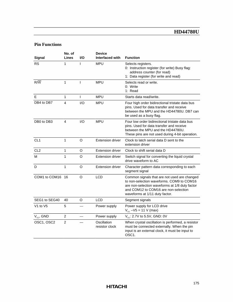
HD44780U
175
Pin Functions
SignalNo. ofLines I/O
DeviceInterfaced with Function
RS 1 I MPU Selects registers.0: Instruction register (for write) Busy flag:
address counter (for read)1: Data register (for write and read)
R/: 1 I MPU Selects read or write.0: Write1: Read
E 1 I MPU Starts data read/write.
DB4 to DB7 4 I/O MPU Four high order bidirectional tristate data buspins. Used for data transfer and receivebetween the MPU and the HD44780U. DB7 canbe used as a busy flag.
DB0 to DB3 4 I/O MPU Four low order bidirectional tristate data buspins. Used for data transfer and receivebetween the MPU and the HD44780U.These pins are not used during 4-bit operation.
CL1 1 O Extension driver Clock to latch serial data D sent to theextension driver
CL2 1 O Extension driver Clock to shift serial data D
M 1 O Extension driver Switch signal for converting the liquid crystaldrive waveform to AC
D 1 O Extension driver Character pattern data corresponding to eachsegment signal
COM1 to COM16 16 O LCD Common signals that are not used are changedto non-selection waveforms. COM9 to COM16are non-selection waveforms at 1/8 duty factorand COM12 to COM16 are non-selectionwaveforms at 1/11 duty factor.
SEG1 to SEG40 40 O LCD Segment signals
V1 to V5 5 — Power supply Power supply for LCD driveVCC –V5 = 11 V (max)
VCC, GND 2 — Power supply VCC: 2.7V to 5.5V, GND: 0V
OSC1, OSC2 2 — Oscillationresistor clock
When crystal oscillation is performed, a resistormust be connected externally. When the pininput is an external clock, it must be input toOSC1.
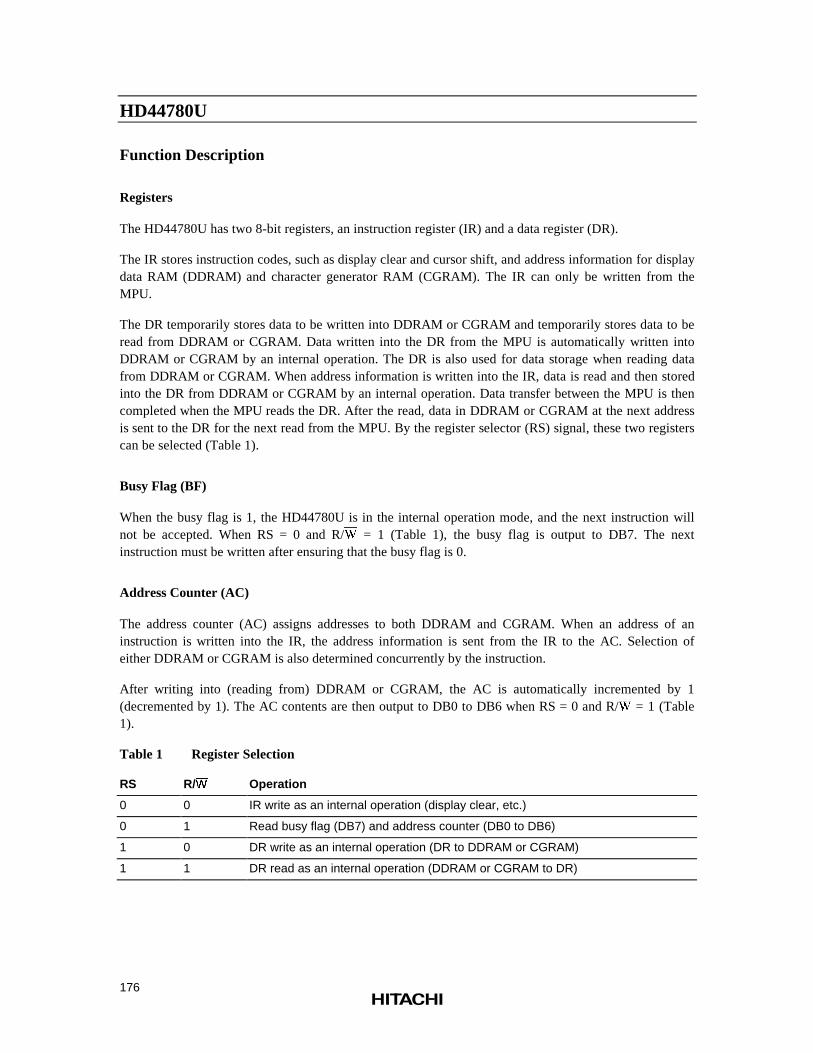
HD44780U
176
Function Description
Registers
The HD44780U has two 8-bit registers, an instruction register (IR) and a data register (DR).
The IR stores instruction codes, such as display clear and cursor shift, and address information for displaydata RAM (DDRAM) and character generator RAM (CGRAM). The IR can only be written from theMPU.
The DR temporarily stores data to be written into DDRAM or CGRAM and temporarily stores data to beread from DDRAM or CGRAM. Data written into the DR from the MPU is automatically written intoDDRAM or CGRAM by an internal operation. The DR is also used for data storage when reading datafrom DDRAM or CGRAM. When address information is written into the IR, data is read and then storedinto the DR from DDRAM or CGRAM by an internal operation. Data transfer between the MPU is thencompleted when the MPU reads the DR. After the read, data in DDRAM or CGRAM at the next addressis sent to the DR for the next read from the MPU. By the register selector (RS) signal, these two registerscan be selected (Table 1).
Busy Flag (BF)
When the busy flag is 1, the HD44780U is in the internal operation mode, and the next instruction willnot be accepted. When RS = 0 and R/: = 1 (Table 1), the busy flag is output to DB7. The nextinstruction must be written after ensuring that the busy flag is 0.
Address Counter (AC)
The address counter (AC) assigns addresses to both DDRAM and CGRAM. When an address of aninstruction is written into the IR, the address information is sent from the IR to the AC. Selection ofeither DDRAM or CGRAM is also determined concurrently by the instruction.
After writing into (reading from) DDRAM or CGRAM, the AC is automatically incremented by 1(decremented by 1). The AC contents are then output to DB0 to DB6 when RS = 0 and R/: = 1 (Table1).
Table 1 Register Selection
RS R/:: Operation
0 0 IR write as an internal operation (display clear, etc.)
0 1 Read busy flag (DB7) and address counter (DB0 to DB6)
1 0 DR write as an internal operation (DR to DDRAM or CGRAM)
1 1 DR read as an internal operation (DDRAM or CGRAM to DR)
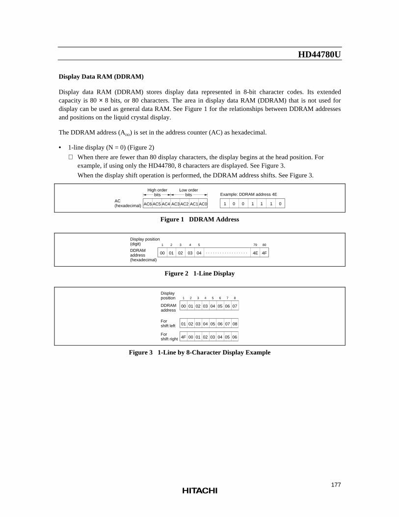
HD44780U
177
Display Data RAM (DDRAM)
Display data RAM (DDRAM) stores display data represented in 8-bit character codes. Its extendedcapacity is 80 × 8 bits, or 80 characters. The area in display data RAM (DDRAM) that is not used fordisplay can be used as general data RAM. See Figure 1 for the relationships between DDRAM addressesand positions on the liquid crystal display.
The DDRAM address (ADD) is set in the address counter (AC) as hexadecimal.
• 1-line display (N = 0) (Figure 2)
When there are fewer than 80 display characters, the display begins at the head position. Forexample, if using only the HD44780, 8 characters are displayed. See Figure 3.
When the display shift operation is performed, the DDRAM address shifts. See Figure 3.
AC6 AC5 AC4 AC3 AC2 AC1 AC0 1 0 0 1 1 1 0AC(hexadecimal)
Example: DDRAM address 4EHigh order
bitsLow order
bits
Figure 1 DDRAM Address
00 01 02 03 04 4E 4FDDRAMaddress(hexadecimal)
Display position(digit) 1 2 3 4 5 79 80
. . . . . . . . . . . . . . . . . .
Figure 2 1-Line Display
DDRAMaddress
Displayposition 1 2 3 4 5 6 7 8
00 01 02 03 04 05 06 07
Forshift left
Forshift right 00 01 02 03 04 05 06
01 02 03 04 05 06 07 08
4F
Figure 3 1-Line by 8-Character Display Example
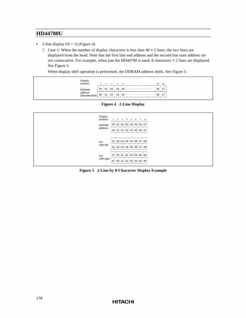
HD44780U
178
• 2-line display (N = 1) (Figure 4)
Case 1: When the number of display characters is less than 40 × 2 lines, the two lines aredisplayed from the head. Note that the first line end address and the second line start address arenot consecutive. For example, when just the HD44780 is used, 8 characters × 2 lines are displayed.See Figure 5.
When display shift operation is performed, the DDRAM address shifts. See Figure 5.
00 01 02 03 04 26 27DDRAMaddress(hexadecimal)
Displayposition 1 2 3 4 5 39 40
. . . . . . . . . . . . . . . . . .
40 41 42 43 44 66 67. . . . . . . . . . . . . . . . . .
Figure 4 2-Line Display
DDRAMaddress
Displayposition 1 2 3 4 5 6 7 8
00 01 02 03 04 05 06 07
Forshift left
Forshift right
40 41 42 43 44 45 46 47
01 02 03 04 05 06 07 08
41 42 43 44 45 46 47 48
00 01 02 03 04 05 06
40 41 42 43 44 45 46
27
67
Figure 5 2-Line by 8-Character Display Example
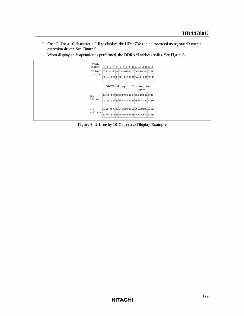
HD44780U
179
Case 2: For a 16-character × 2-line display, the HD44780 can be extended using one 40-outputextension driver. See Figure 6.
When display shift operation is performed, the DDRAM address shifts. See Figure 6.
DDRAMaddress
Displayposition 1 2 3 4 5 6 7 8 9 10 11 12 13 14 15 16
00 01 02 03 04 05 06 07 08 09 0A 0B0C0D 0E 0F
Forshift left
00 01 02 03 04 05 06 07 08 09 0A 0B0C0D 0E27
40 41 42 43 44 45 46 47 48 49 4A 4B4C4D 4E 4F
HD44780U display Extension driverdisplay
0201 03 04 05 06 07 08 09 0A 0B0C0D 0E 0F10
Forshift right
41 42 43 44 45 46 47 48 49 4A 4B4C4D 4E 4F 50
40 41 42 43 44 45 46 47 48 49 4A 4B4C4D 4E67
Figure 6 2-Line by 16-Character Display Example
HD44780U
180
Character Generator ROM (CGROM)
The character generator ROM generates 5 × 8 dot or 5 × 10 dot character patterns from 8-bit charactercodes (Table 4). It can generate 208 5 × 8 dot character patterns and 32 5 × 10 dot character patterns.User-defined character patterns are also available by mask-programmed ROM.
Character Generator RAM (CGRAM)
In the character generator RAM, the user can rewrite character patterns by program. For 5 × 8 dots, eightcharacter patterns can be written, and for 5 × 10 dots, four character patterns can be written.
Write into DDRAM the character codes at the addresses shown as the left column of Table 4 to show thecharacter patterns stored in CGRAM.
See Table 5 for the relationship between CGRAM addresses and data and display patterns.
Areas that are not used for display can be used as general data RAM.
Modifying Character Patterns
• Character pattern development procedure
The following operations correspond to the numbers listed in Figure 7:
1. Determine the correspondence between character codes and character patterns.
2. Create a listing indicating the correspondence between EPROM addresses and data.
3. Program the character patterns into the EPROM.
4. Send the EPROM to Hitachi.
5. Computer processing on the EPROM is performed at Hitachi to create a character pattern listing,which is sent to the user.
6. If there are no problems within the character pattern listing, a trial LSI is created at Hitachi andsamples are sent to the user for evaluation. When it is confirmed by the user that the characterpatterns are correctly written, mass production of the LSI proceeds at Hitachi.
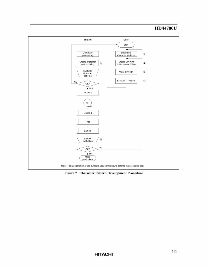
HD44780U
181
Determinecharacter patterns
Create EPROMaddress data listing
Write EPROM
EPROM → Hitachi
Computerprocessing
Create characterpattern listing
Evaluatecharacterpatterns
OK?
Art work
Sampleevaluation
OK?
Masking
Trial
Sample
No
Yes
No
Yes
M/T
1
3
2
4
5
6
Note: For a description of the numbers used in this figure, refer to the preceding page.
UserHitachi
Massproduction
Start
Figure 7 Character Pattern Development Procedure
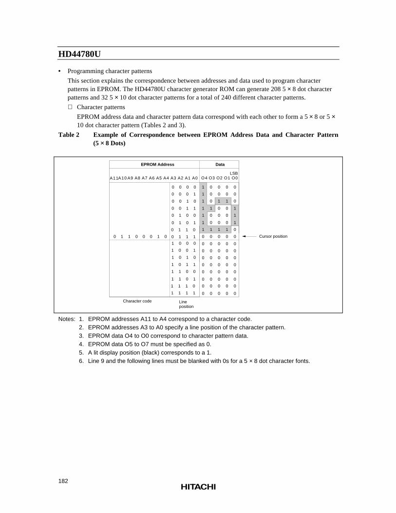
HD44780U
182
• Programming character patterns
This section explains the correspondence between addresses and data used to program characterpatterns in EPROM. The HD44780U character generator ROM can generate 208 5 × 8 dot characterpatterns and 32 5 × 10 dot character patterns for a total of 240 different character patterns.
Character patterns
EPROM address data and character pattern data correspond with each other to form a 5 × 8 or 5 ×10 dot character pattern (Tables 2 and 3).
Table 2 Example of Correspondence between EPROM Address Data and Character Pattern(5 ×× 8 Dots)
Data
O4 O3 O2 O1 O0
0 0 0 1
0 0 1 0
0 0 1 1
0 1 0 0
0 1 1 0 0 0 1 0
EPROM Address
Character code Line position
LSB
0 1 0 1
0 1 1 0
0 1 1 1
0 0 0 0
1 0 0 1
1 0 1 0
1 0 1 1
1 1 0 0
1 1 0 1
1 1 1 0
1 1 1 1
1 0 0 0
1 1 0 0 1
1 0 0 0 1
1 0 0 0 1
1 0 0 0 0
1 0 0 0 0
1 0 1 1 0
Cursor position
1 1 1 1 0
0 0 0 0 0
0 0 0 0 0
0 0 0 0 0
0 0 0 0 0
0 0 0 0 0
0 0 0 0 0
0 0 0 0 0
0 0 0 0 0
0 0 0 0 0
A10 A9 A8 A7 A6 A5 A4 A3 A2 A1 A0A11
Notes: 1. EPROM addresses A11 to A4 correspond to a character code.2. EPROM addresses A3 to A0 specify a line position of the character pattern.3. EPROM data O4 to O0 correspond to character pattern data.4. EPROM data O5 to O7 must be specified as 0.5. A lit display position (black) corresponds to a 1.6. Line 9 and the following lines must be blanked with 0s for a 5 × 8 dot character fonts.
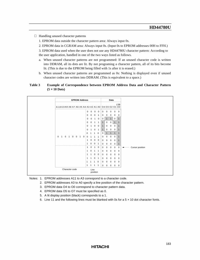
HD44780U
183
Handling unused character patterns
1. EPROM data outside the character pattern area: Always input 0s.
2. EPROM data in CGRAM area: Always input 0s. (Input 0s to EPROM addresses 00H to FFH.)
3. EPROM data used when the user does not use any HD44780U character pattern: According tothe user application, handled in one of the two ways listed as follows.
a. When unused character patterns are not programmed: If an unused character code is writteninto DDRAM, all its dots are lit. By not programing a character pattern, all of its bits becomelit. (This is due to the EPROM being filled with 1s after it is erased.)
b. When unused character patterns are programmed as 0s: Nothing is displayed even if unusedcharacter codes are written into DDRAM. (This is equivalent to a space.)
Table 3 Example of Correspondence between EPROM Address Data and Character Pattern(5 ×× 10 Dots)
A10 A9 A8 A7 A6 A5 A4 A3 A2 A1 A0
Data
O4 O3 O2 O1 O0
0 0 0 1
0 0 1 0
0 0 1 1
0 1 0 0
0 1 0 1 0 0 1 0
EPROM Address
Character code Line position
LSB
0 1 0 1
0 1 1 0
0 1 1 1
0 0 0 0 0
0 0 0 0 0
0 1 1 0 1
1 0 0 1 1
1 0 0 0 1
1 0 0 0 1
0 0 0 0
A11
1 0 0 1
1 0 1 0
1 0 1 1
1 1 0 0
1 1 0 1
1 1 1 0
1 1 1 1
1 0 0 0
Cursor position0 0 0 0 0
0 0 0 0 0
0 0 0 0 0
0 0 0 0 0
0 0 0 0 0
0 0 0 0 0
0 0 0 0 1
0 0 0 0 1
0 0 0 0 1
0 1 1 1 1
Notes: 1. EPROM addresses A11 to A3 correspond to a character code.2. EPROM addresses A3 to A0 specify a line position of the character pattern.3. EPROM data O4 to O0 correspond to character pattern data.4. EPROM data O5 to O7 must be specified as 0.5. A lit display position (black) corresponds to a 1.6. Line 11 and the following lines must be blanked with 0s for a 5 × 10 dot character fonts.
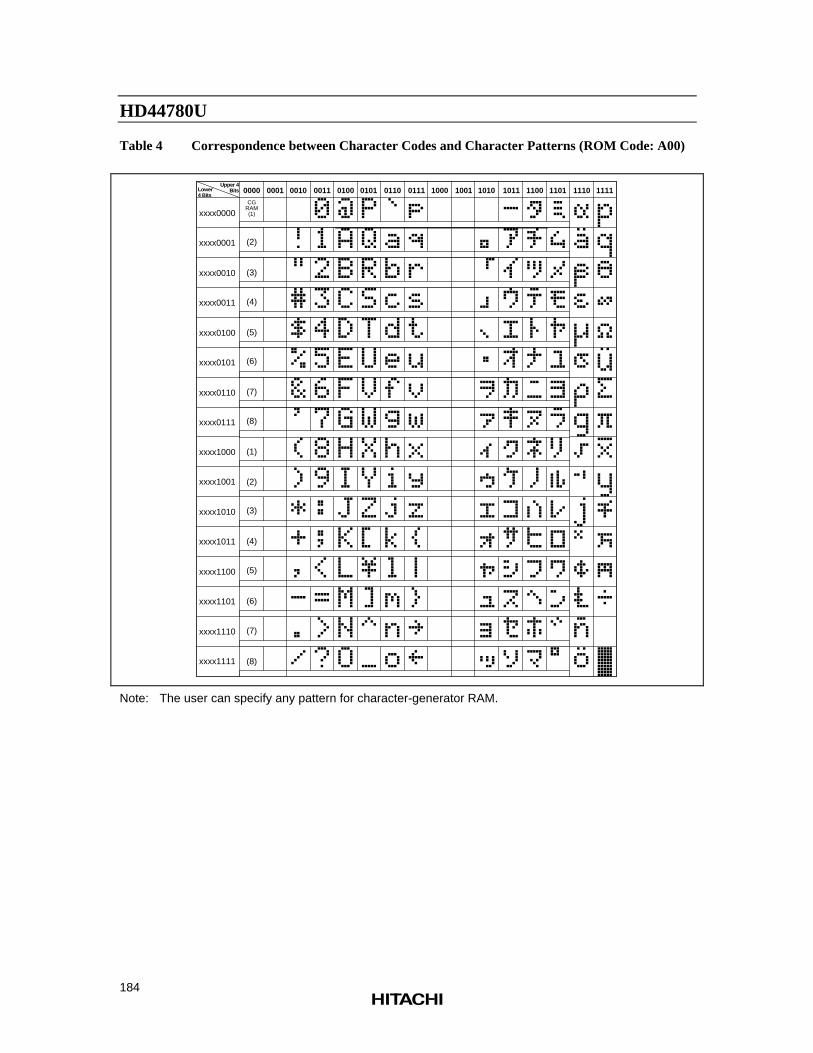
HD44780U
184
Table 4 Correspondence between Character Codes and Character Patterns (ROM Code: A00)
xxxx0000
xxxx0001
xxxx0010
xxxx0011
xxxx0100
xxxx0101
xxxx0110
xxxx0111
xxxx1000
xxxx1001
xxxx1010
xxxx1011
xxxx1100
xxxx1101
xxxx1110
xxxx1111
0000 0010 0011 0100 0101 0110 0111 1010 1011 1100 1101 1110 1111Upper 4
BitsLower 4 Bits
CG RAM (1)
(2)
(3)
(4)
(5)
(6)
(7)
(8)
(1)
(2)
(3)
(4)
(5)
(6)
(7)
(8)
0001 1000 1001
Note: The user can specify any pattern for character-generator RAM.
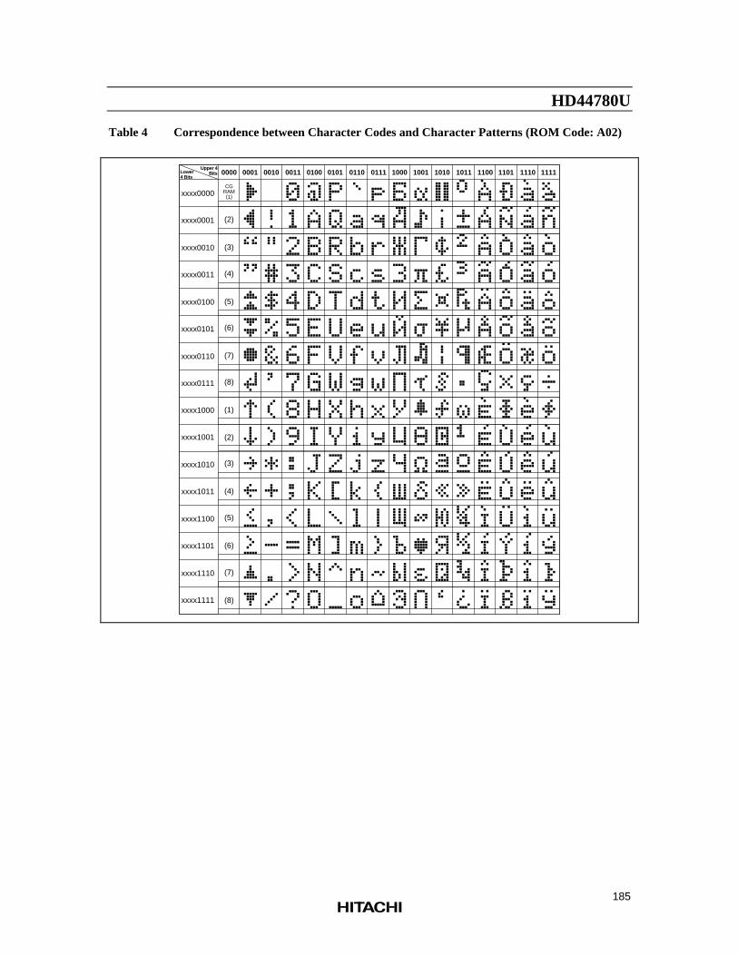
HD44780U
185
Table 4 Correspondence between Character Codes and Character Patterns (ROM Code: A02)
xxxx0000
xxxx0001
xxxx0010
xxxx0011
xxxx0100
xxxx0101
xxxx0110
xxxx0111
xxxx1000
xxxx1001
xxxx1010
xxxx1011
xxxx1100
xxxx1101
xxxx1110
xxxx1111
0000 0010 0011 0100 0101 0110 0111 1010 1011 1100 1101 1110 1111Upper 4
BitsLower 4 Bits
CG RAM (1)
(2)
(3)
(4)
(5)
(6)
(7)
(8)
(1)
(2)
(3)
(4)
(5)
(6)
(7)
(8)
0001 1000 1001
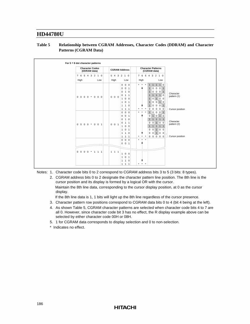
HD44780U
186
Table 5 Relationship between CGRAM Addresses, Character Codes (DDRAM) and CharacterPatterns (CGRAM Data)
Character Codes (DDRAM data) CGRAM Address
Character Patterns (CGRAM data)
7 6 5 4 3 2 1 0
0 0 0 0 * 0 0 0
0 0 0 0 * 0 0 1
0 0 0 0 * 1 1 1
5 4 3 2 1 0
0 0 0
0 0 1
1 1 1
7 6 5 4 3 2 1 0
0
0
0
0
1
1
1
1
0
0
0
0
1
1
1
1
0
0
1
1
1
1
0
0
1
1
0
0
1
1
0
0
1
1
0
0
1
1
0
0
0
0
1
1
0
1
0
1
0
1
0
1
0
1
0
1
0
1
0
1
0
1
0
1
0
1
*
*
*
*
*
*
*
*
*
*
*
*
*
*
*
*
*
*
High Low High Low High Low
Characterpattern (1)
Cursor position
1
1
1
1
1
1
1
0
1
0
1
0
1
0
0
0
0
1
1
0
0
0
1
0
1
0
1
0
1
0
0
0
1
0
0
1
0
0
0
0
0
1
1
0
1
0
0
0
1
0
0
1
1
0
0
0
0
0
1
1
1
1
1
0
1
0
0
1
0
1
0
0
0
1
1
0
1
0
0
0
Characterpattern (2)
Cursor position
For 5 × 8 dot character patterns
Notes: 1. Character code bits 0 to 2 correspond to CGRAM address bits 3 to 5 (3 bits: 8 types).2. CGRAM address bits 0 to 2 designate the character pattern line position. The 8th line is the
cursor position and its display is formed by a logical OR with the cursor.Maintain the 8th line data, corresponding to the cursor display position, at 0 as the cursordisplay.If the 8th line data is 1, 1 bits will light up the 8th line regardless of the cursor presence.
3. Character pattern row positions correspond to CGRAM data bits 0 to 4 (bit 4 being at the left).4. As shown Table 5, CGRAM character patterns are selected when character code bits 4 to 7 are
all 0. However, since character code bit 3 has no effect, the R display example above can beselected by either character code 00H or 08H.
5. 1 for CGRAM data corresponds to display selection and 0 to non-selection.* Indicates no effect.
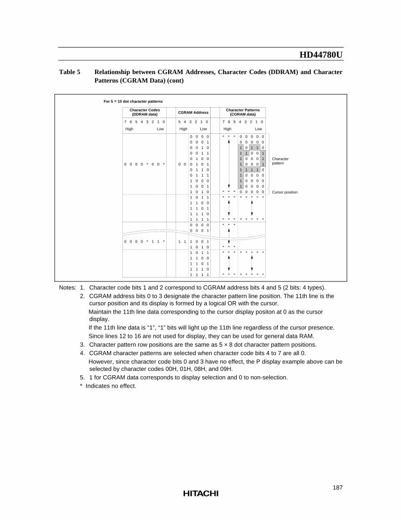
HD44780U
187
Table 5 Relationship between CGRAM Addresses, Character Codes (DDRAM) and CharacterPatterns (CGRAM Data) (cont)
Character Codes (DDRAM data) CGRAM Address
Character Patterns (CGRAM data)
7 6 5 4 3 2 1 0
0 0 0 0 * 0 0
0 0 0 0 1 1
5 4 3 2 1 0
0 0
1 1
7 6 5 4 3 2 1 0
*
*
*
*
*
*
*
*
*
*
*
*
*
*
*
*
*
*
*
*
*
*
*
*
High Low High Low High Low
Characterpattern
Cursor position
0
0
0
0
1
1
1
1
0
0
0
0
1
1
1
1
0
0
0
0
0
1
1
1
1
0
0
1
1
0
0
1
1
0
0
1
1
0
0
1
1
0
0
0
1
1
0
0
1
1
0
1
0
1
0
1
0
1
0
1
0
1
0
1
0
1
0
1
1
0
1
0
1
0
1
0
0
0
0
0
0
0
0
1
1
1
1
1
1
1
1
0
0
1
1
1
1
1
1
1
*
*
*
*
*
* *
0
0
1
1
1
1
1
1
1
1
0
0
0
0
1
0
0
1
0
0
0
0
0
0
1
0
0
0
1
0
0
0
0
0
0
1
0
0
0
1
0
0
0
0
0
0
0
1
1
1
0
0
0
0
0
*
*
*
*
*
*
*
*
*
*
*
*
*
*
*
*
For 5 × 10 dot character patterns
Notes: 1. Character code bits 1 and 2 correspond to CGRAM address bits 4 and 5 (2 bits: 4 types).2. CGRAM address bits 0 to 3 designate the character pattern line position. The 11th line is the
cursor position and its display is formed by a logical OR with the cursor.Maintain the 11th line data corresponding to the cursor display positon at 0 as the cursordisplay.If the 11th line data is “1”, “1” bits will light up the 11th line regardless of the cursor presence.Since lines 12 to 16 are not used for display, they can be used for general data RAM.
3. Character pattern row positions are the same as 5 × 8 dot character pattern positions.4. CGRAM character patterns are selected when character code bits 4 to 7 are all 0.
However, since character code bits 0 and 3 have no effect, the P display example above can beselected by character codes 00H, 01H, 08H, and 09H.
5. 1 for CGRAM data corresponds to display selection and 0 to non-selection.* Indicates no effect.
HD44780U
188
Timing Generation Circuit
The timing generation circuit generates timing signals for the operation of internal circuits such asDDRAM, CGROM and CGRAM. RAM read timing for display and internal operation timing by MPUaccess are generated separately to avoid interfering with each other. Therefore, when writing data toDDRAM, for example, there will be no undesirable interferences, such as flickering, in areas other thanthe display area.
Liquid Crystal Display Driver Circuit
The liquid crystal display driver circuit consists of 16 common signal drivers and 40 segment signaldrivers. When the character font and number of lines are selected by a program, the required commonsignal drivers automatically output drive waveforms, while the other common signal drivers continue tooutput non-selection waveforms.
Sending serial data always starts at the display data character pattern corresponding to the last address ofthe display data RAM (DDRAM).
Since serial data is latched when the display data character pattern corresponding to the starting addressenters the internal shift register, the HD44780U drives from the head display.
Cursor/Blink Control Circuit
The cursor/blink control circuit generates the cursor or character blinking. The cursor or the blinking willappear with the digit located at the display data RAM (DDRAM) address set in the address counter (AC).
For example (Figure 8), when the address counter is 08H, the cursor position is displayed at DDRAMaddress 08H.
AC6
0
AC5
0
AC4
0
AC3
1
AC2
0
AC1
0
AC0
0
1
00
2
01
3
02
4
03
5
04
6
05
7
06
8
07
9
08
10
09
11
0A
1
00
40
2
01
41
3
02
42
4
03
43
5
04
44
6
05
45
7
06
46
8
07
47
9
08
48
10
09
49
11
0A
4A
AC
cursor position
cursor position
Display position
DDRAM address (hexadecimal)
Display position
DDRAM address (hexadecimal)
For a 1-line display
For a 2-line display
Note: The cursor or blinking appears when the address counter (AC) selects the character generator RAM (CGRAM). However, the cursor and blinking become meaningless. The cursor or blinking is displayed in the meaningless position when the AC is a CGRAM address.
Figure 8 Cursor/Blink Display Example
HD44780U
189
Interfacing to the MPU
The HD44780U can send data in either two 4-bit operations or one 8-bit operation, thus allowinginterfacing with 4- or 8-bit MPUs.
• For 4-bit interface data, only four bus lines (DB4 to DB7) are used for transfer. Bus lines DB0 to DB3are disabled. The data transfer between the HD44780U and the MPU is completed after the 4-bit datahas been transferred twice. As for the order of data transfer, the four high order bits (for 8-bitoperation, DB4 to DB7) are transferred before the four low order bits (for 8-bit operation, DB0 toDB3).
The busy flag must be checked (one instruction) after the 4-bit data has been transferred twice. Twomore 4-bit operations then transfer the busy flag and address counter data.
• For 8-bit interface data, all eight bus lines (DB0 to DB7) are used.
RS
R/W
E
IR7
IR6
IR5
IR4
BF
AC6
AC5
AC4
DB7
DB6
DB5
DB4
Instruction register (IR) write
Busy flag (BF) and address counter (AC) read
Data register (DR) read
IR3
IR2
IR1
IR0
AC3
AC2
AC1
AC0
DR7
DR6
DR5
DR4
DR3
DR2
DR1
DR0
Figure 9 4-Bit Transfer Example
HD44780U
190
Reset Function
Initializing by Internal Reset Circuit
An internal reset circuit automatically initializes the HD44780U when the power is turned on. Thefollowing instructions are executed during the initialization. The busy flag (BF) is kept in the busy stateuntil the initialization ends (BF = 1). The busy state lasts for 10 ms after VCC rises to 4.5 V.
1. Display clear
2. Function set:
DL = 1; 8-bit interface data
N = 0; 1-line display
F = 0; 5 × 8 dot character font
3. Display on/off control:
D = 0; Display off
C = 0; Cursor off
B = 0; Blinking off
4. Entry mode set:
I/D = 1; Increment by 1
S = 0; No shift
Note: If the electrical characteristics conditions listed under the table Power Supply Conditions UsingInternal Reset Circuit are not met, the internal reset circuit will not operate normally and will failto initialize the HD44780U. For such a case, initial-ization must be performed by the MPU asexplained in the section, Initializing by Instruction.
Instructions
Outline
Only the instruction register (IR) and the data register (DR) of the HD44780U can be controlled by theMPU. Before starting the internal operation of the HD44780U, control information is temporarily storedinto these registers to allow interfacing with various MPUs, which operate at different speeds, or variousperipheral control devices. The internal operation of the HD44780U is determined by signals sent fromthe MPU. These signals, which include register selection signal (RS), read/
write signal (R/:), and the data bus (DB0 to DB7), make up the HD44780U instructions (Table 6). Thereare four categories of instructions that:
• Designate HD44780U functions, such as display format, data length, etc.
• Set internal RAM addresses
• Perform data transfer with internal RAM
• Perform miscellaneous functions
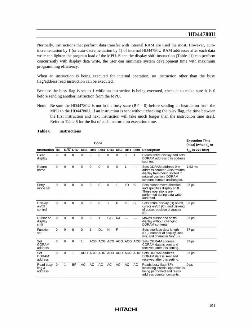
HD44780U
191
Normally, instructions that perform data transfer with internal RAM are used the most. However, auto-incrementation by 1 (or auto-decrementation by 1) of internal HD44780U RAM addresses after each datawrite can lighten the program load of the MPU. Since the display shift instruction (Table 11) can performconcurrently with display data write, the user can minimize system development time with maximumprogramming efficiency.
When an instruction is being executed for internal operation, no instruction other than the busyflag/address read instruction can be executed.
Because the busy flag is set to 1 while an instruction is being executed, check it to make sure it is 0before sending another instruction from the MPU.
Note: Be sure the HD44780U is not in the busy state (BF = 0) before sending an instruction from theMPU to the HD44780U. If an instruction is sent without checking the busy flag, the time betweenthe first instruction and next instruction will take much longer than the instruction time itself.Refer to Table 6 for the list of each instruc-tion execution time.
Table 6 Instructions
CodeExecution Time(max) (when f cp or
Instruction RS R/ :: DB7 DB6 DB5 DB4 DB3 DB2 DB1 DB0 Description f OSC is 270 kHz)
Cleardisplay
0 0 0 0 0 0 0 0 0 1 Clears entire display and setsDDRAM address 0 in addresscounter.
Returnhome
0 0 0 0 0 0 0 0 1 — Sets DDRAM address 0 inaddress counter. Also returnsdisplay from being shifted tooriginal position. DDRAMcontents remain unchanged.
1.52 ms
Entrymode set
0 0 0 0 0 0 0 1 I/D S Sets cursor move directionand specifies display shift.These operations areperformed during data writeand read.
37 µs
Displayon/offcontrol
0 0 0 0 0 0 1 D C B Sets entire display (D) on/off,cursor on/off (C), and blinkingof cursor position character(B).
37 µs
Cursor ordisplayshift
0 0 0 0 0 1 S/C R/L — — Moves cursor and shiftsdisplay without changingDDRAM contents.
37 µs
Functionset
0 0 0 0 1 DL N F — — Sets interface data length(DL), number of display lines(N), and character font (F).
37 µs
SetCGRAMaddress
0 0 0 1 ACG ACG ACG ACG ACG ACG Sets CGRAM address.CGRAM data is sent andreceived after this setting.
37 µs
SetDDRAMaddress
0 0 1 ADD ADD ADD ADD ADD ADD ADD Sets DDRAM address.DDRAM data is sent andreceived after this setting.
37 µs
Read busyflag &address
0 1 BF AC AC AC AC AC AC AC Reads busy flag (BF)indicating internal operation isbeing performed and readsaddress counter contents.
0 µs
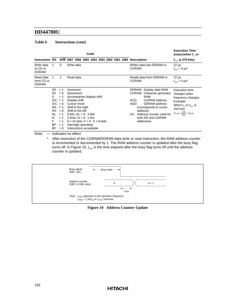
HD44780U
192
Table 6 Instructions (cont)
CodeExecution Time(max) (when f cp or
Instruction RS R/ :: DB7 DB6 DB5 DB4 DB3 DB2 DB1 DB0 Description f OSC is 270 kHz)
Write datato CG orDDRAM
1 0 Write data Writes data into DDRAM orCGRAM.
37 µstADD = 4 µs*
Read datafrom CG orDDRAM
1 1 Read data Reads data from DDRAM orCGRAM.
37 µstADD = 4 µs*
I/D = 1: IncrementI/D = 0: DecrementS = 1: Accompanies display shiftS/C = 1: Display shiftS/C = 0: Cursor moveR/L = 1: Shift to the rightR/L = 0: Shift to the leftDL = 1: 8 bits, DL = 0: 4 bitsN = 1: 2 lines, N = 0: 1 lineF = 1: 5 × 10 dots, F = 0: 5 × 8 dotsBF = 1: Internally operatingBF = 0: Instructions acceptable
DDRAM: Display data RAMCGRAM: Character generator
RAMACG: CGRAM addressADD: DDRAM address
(corresponds to cursoraddress)
AC: Address counter used forboth DD and CGRAMaddresses
Execution timechanges whenfrequency changesExample:When fcp or fOSC is250 kHz,37 µs × = 40 µs270
250
Note: — indicates no effect.* After execution of the CGRAM/DDRAM data write or read instruction, the RAM address counter
is incremented or decremented by 1. The RAM address counter is updated after the busy flagturns off. In Figure 10, tADD is the time elapsed after the busy flag turns off until the addresscounter is updated.
Busy stateBusy signal (DB7 pin)
Address counter (DB0 to DB6 pins)
t ADD
A A + 1
Note: t depends on the operation frequency t = 1.5/(f or f ) seconds
ADD
ADD cp OSC
Figure 10 Address Counter Update
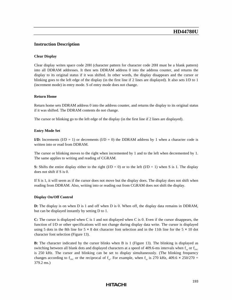
HD44780U
193
Instruction Description
Clear Display
Clear display writes space code 20H (character pattern for character code 20H must be a blank pattern)into all DDRAM addresses. It then sets DDRAM address 0 into the address counter, and returns thedisplay to its original status if it was shifted. In other words, the display disappears and the cursor orblinking goes to the left edge of the display (in the first line if 2 lines are displayed). It also sets I/D to 1(increment mode) in entry mode. S of entry mode does not change.
Return Home
Return home sets DDRAM address 0 into the address counter, and returns the display to its original statusif it was shifted. The DDRAM contents do not change.
The cursor or blinking go to the left edge of the display (in the first line if 2 lines are displayed).
Entry Mode Set
I/D: Increments (I/D = 1) or decrements (I/D = 0) the DDRAM address by 1 when a character code iswritten into or read from DDRAM.
The cursor or blinking moves to the right when incremented by 1 and to the left when decremented by 1.The same applies to writing and reading of CGRAM.
S: Shifts the entire display either to the right (I/D = 0) or to the left (I/D = 1) when S is 1. The displaydoes not shift if S is 0.
If S is 1, it will seem as if the cursor does not move but the display does. The display does not shift whenreading from DDRAM. Also, writing into or reading out from CGRAM does not shift the display.
Display On/Off Control
D: The display is on when D is 1 and off when D is 0. When off, the display data remains in DDRAM,but can be displayed instantly by setting D to 1.
C: The cursor is displayed when C is 1 and not displayed when C is 0. Even if the cursor disappears, thefunction of I/D or other specifications will not change during display data write. The cursor is displayedusing 5 dots in the 8th line for 5 × 8 dot character font selection and in the 11th line for the 5 × 10 dotcharacter font selection (Figure 13).
B: The character indicated by the cursor blinks when B is 1 (Figure 13). The blinking is displayed asswitching between all blank dots and displayed characters at a speed of 409.6-ms intervals when fcp or fOSC
is 250 kHz. The cursor and blinking can be set to display simultaneously. (The blinking frequencychanges according to fOSC or the reciprocal of fcp. For example, when fcp is 270 kHz, 409.6 × 250/270 =379.2 ms.)
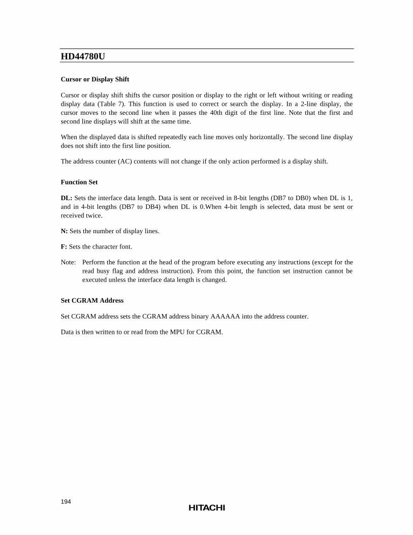
HD44780U
194
Cursor or Display Shift
Cursor or display shift shifts the cursor position or display to the right or left without writing or readingdisplay data (Table 7). This function is used to correct or search the display. In a 2-line display, thecursor moves to the second line when it passes the 40th digit of the first line. Note that the first andsecond line displays will shift at the same time.
When the displayed data is shifted repeatedly each line moves only horizontally. The second line displaydoes not shift into the first line position.
The address counter (AC) contents will not change if the only action performed is a display shift.
Function Set
DL: Sets the interface data length. Data is sent or received in 8-bit lengths (DB7 to DB0) when DL is 1,and in 4-bit lengths (DB7 to DB4) when DL is 0.When 4-bit length is selected, data must be sent orreceived twice.
N: Sets the number of display lines.
F: Sets the character font.
Note: Perform the function at the head of the program before executing any instructions (except for theread busy flag and address instruction). From this point, the function set instruction cannot beexecuted unless the interface data length is changed.
Set CGRAM Address
Set CGRAM address sets the CGRAM address binary AAAAAA into the address counter.
Data is then written to or read from the MPU for CGRAM.
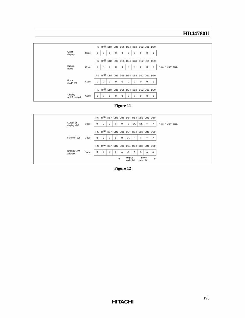
HD44780U
195
Code Note: Don’t care.*
Code
Code
Code
RS
0
R/W
0
DB7
0
DB6
0
DB5
0
DB4
0
DB3
0
DB2
0
DB1
0
DB0
1
RS
0
R/W
0
DB7
0
DB6
0
DB5
0
DB4
0
DB3
0
DB2
0
DB1
0
DB0
1
RS
0
R/W
0
DB7
0
DB6
0
DB5
0
DB4
0
DB3
0
DB2
0
DB1
0
DB0
1
RS
0
R/W
0
DB7
0
DB6
0
DB5
0
DB4
0
DB3
0
DB2
0
DB1
0
DB0
1
Return home
Clear display
Entry mode set
Display on/off control
Figure 11
RS
0
R/W
0
DB7
0
DB6
0
DB5
0
DB4
1
DB3
S/CCode
DB2
R/L
DB1 DB0
Code
Code
Higherorder bit
Lowerorder bit
*Cursor ordisplay shift
Function set
Set CGRAM address
*
RS
0
R/W
0
DB7
0
DB6
0
DB5
0
DB4
DL
DB3
N
DB2
F
DB1 DB0
* *
RS
0
R/W
0
DB7
0
DB6
0
DB5
A
DB4
A
DB3
A
DB2
A
DB1 DB0
A A
Note: Don’t care.*
Figure 12
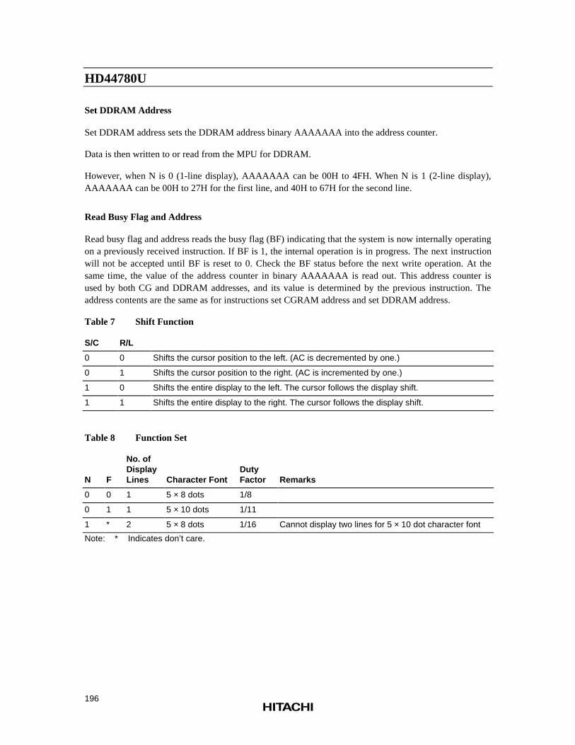
HD44780U
196
Set DDRAM Address
Set DDRAM address sets the DDRAM address binary AAAAAAA into the address counter.
Data is then written to or read from the MPU for DDRAM.
However, when N is 0 (1-line display), AAAAAAA can be 00H to 4FH. When N is 1 (2-line display),AAAAAAA can be 00H to 27H for the first line, and 40H to 67H for the second line.
Read Busy Flag and Address
Read busy flag and address reads the busy flag (BF) indicating that the system is now internally operatingon a previously received instruction. If BF is 1, the internal operation is in progress. The next instructionwill not be accepted until BF is reset to 0. Check the BF status before the next write operation. At thesame time, the value of the address counter in binary AAAAAAA is read out. This address counter isused by both CG and DDRAM addresses, and its value is determined by the previous instruction. Theaddress contents are the same as for instructions set CGRAM address and set DDRAM address.
Table 7 Shift Function
S/C R/L
0 0 Shifts the cursor position to the left. (AC is decremented by one.)
0 1 Shifts the cursor position to the right. (AC is incremented by one.)
1 0 Shifts the entire display to the left. The cursor follows the display shift.
1 1 Shifts the entire display to the right. The cursor follows the display shift.
Table 8 Function Set
N F
No. ofDisplayLines Character Font
DutyFactor Remarks
0 0 1 5 × 8 dots 1/8
0 1 1 5 × 10 dots 1/11
1 * 2 5 × 8 dots 1/16 Cannot display two lines for 5 × 10 dot character font
Note: * Indicates don’t care.
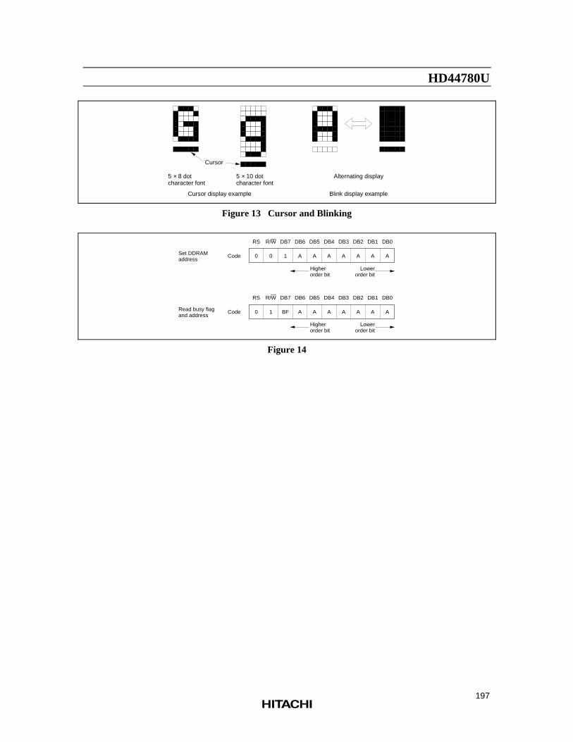
HD44780U
197
Cursor
5 8 dot character font
5 10 dot character font
× × Alternating display
Blink display exampleCursor display example
Figure 13 Cursor and Blinking
RS
0
R/W
0
DB7
1
DB6
A
DB5
A
DB4
A
DB3
ACode
DB2
A
DB1
A
DB0
A
Higherorder bit
Lowerorder bit
RS
0
R/W
1
DB7
BF
DB6
A
DB5
A
DB4
A
DB3
ACode
DB2
A
DB1
A
DB0
A
Higherorder bit
Lowerorder bit
Set DDRAM address
Read busy flagand address
Figure 14
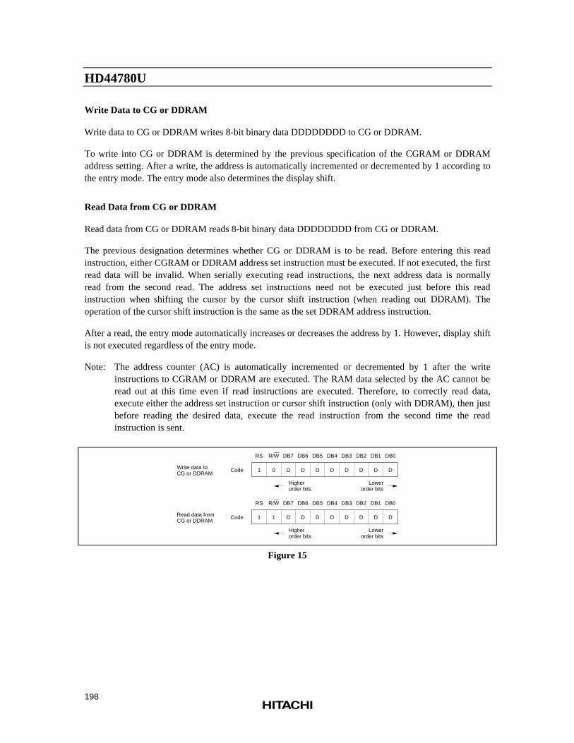
HD44780U
198
Write Data to CG or DDRAM
Write data to CG or DDRAM writes 8-bit binary data DDDDDDDD to CG or DDRAM.
To write into CG or DDRAM is determined by the previous specification of the CGRAM or DDRAMaddress setting. After a write, the address is automatically incremented or decremented by 1 according tothe entry mode. The entry mode also determines the display shift.
Read Data from CG or DDRAM
Read data from CG or DDRAM reads 8-bit binary data DDDDDDDD from CG or DDRAM.
The previous designation determines whether CG or DDRAM is to be read. Before entering this readinstruction, either CGRAM or DDRAM address set instruction must be executed. If not executed, the firstread data will be invalid. When serially executing read instructions, the next address data is normallyread from the second read. The address set instructions need not be executed just before this readinstruction when shifting the cursor by the cursor shift instruction (when reading out DDRAM). Theoperation of the cursor shift instruction is the same as the set DDRAM address instruction.
After a read, the entry mode automatically increases or decreases the address by 1. However, display shiftis not executed regardless of the entry mode.
Note: The address counter (AC) is automatically incremented or decremented by 1 after the writeinstructions to CGRAM or DDRAM are executed. The RAM data selected by the AC cannot beread out at this time even if read instructions are executed. Therefore, to correctly read data,execute either the address set instruction or cursor shift instruction (only with DDRAM), then justbefore reading the desired data, execute the read instruction from the second time the readinstruction is sent.
RS
1
R/W
1
DB7
D
DB6
D
DB5
D
DB4
D
DB3
DCode
DB2
D
DB1
D
DB0
D
Higherorder bits
Lowerorder bits
RS
1
R/W
0
DB7
D
DB6
D
DB5
D
DB4
D
DB3
DCode
DB2
D
DB1
D
DB0
D
Higherorder bits
Lowerorder bits
Read data fromCG or DDRAM
Write data toCG or DDRAM
Figure 15
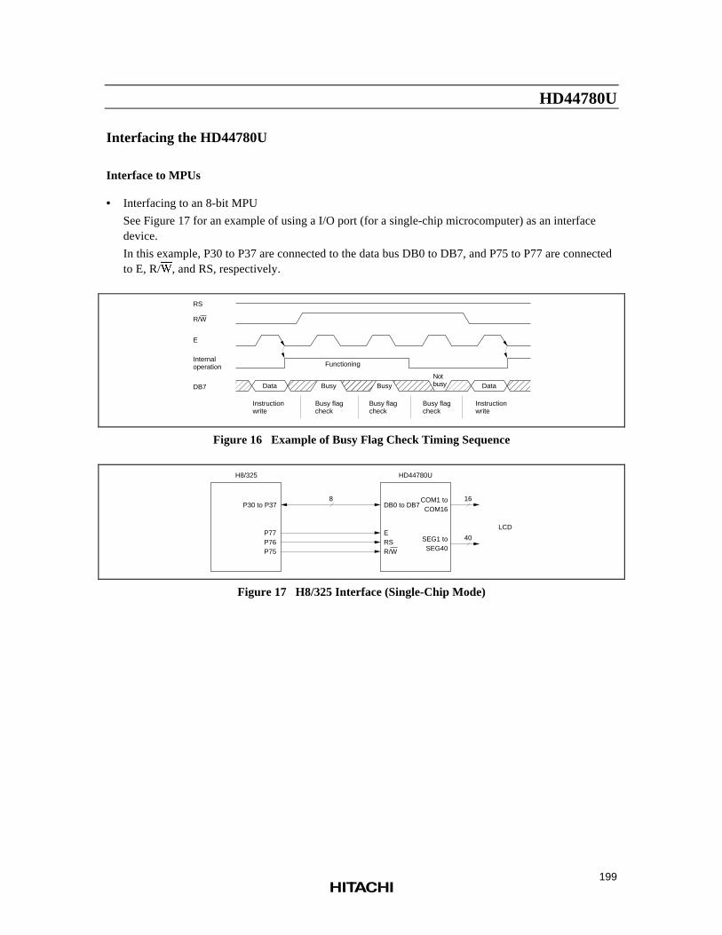
HD44780U
199
Interfacing the HD44780U
Interface to MPUs
• Interfacing to an 8-bit MPU
See Figure 17 for an example of using a I/O port (for a single-chip microcomputer) as an interfacedevice.
In this example, P30 to P37 are connected to the data bus DB0 to DB7, and P75 to P77 are connectedto E, R/:, and RS, respectively.
RS
R/W
E
Internal operation
DB7
Functioning
Data Busy BusyNot busy Data
Instruction write
Busy flag check
Busy flag check
Busy flag check
Instruction write
Figure 16 Example of Busy Flag Check Timing Sequence
P30 to P37
P77 P76 P75
16
40
H8/325 HD44780U
8DB0 to DB7
E RS R/W
LCD
COM1 to COM16
SEG1 to SEG40
Figure 17 H8/325 Interface (Single-Chip Mode)
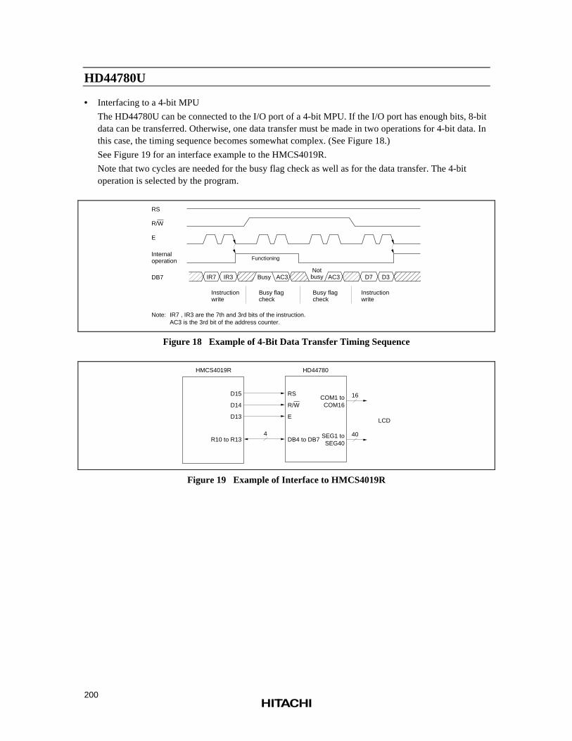
HD44780U
200
• Interfacing to a 4-bit MPU
The HD44780U can be connected to the I/O port of a 4-bit MPU. If the I/O port has enough bits, 8-bitdata can be transferred. Otherwise, one data transfer must be made in two operations for 4-bit data. Inthis case, the timing sequence becomes somewhat complex. (See Figure 18.)
See Figure 19 for an interface example to the HMCS4019R.
Note that two cycles are needed for the busy flag check as well as for the data transfer. The 4-bitoperation is selected by the program.
RS
R/W
E
Internaloperation
DB7 IR7 IR3 Busy AC3Not
busy AC3 D7 D3
Instructionwrite
Busy flagcheck
Busy flagcheck
Instructionwrite
Note: IR7 , IR3 are the 7th and 3rd bits of the instruction.AC3 is the 3rd bit of the address counter.
Functioning
Figure 18 Example of 4-Bit Data Transfer Timing Sequence
D15
D14
D13
R10 to R13
RS
R/W
E
DB4 to DB7
COM1 to COM16
SEG1 to SEG40
4 40
16
LCD
HMCS4019R HD44780
Figure 19 Example of Interface to HMCS4019R
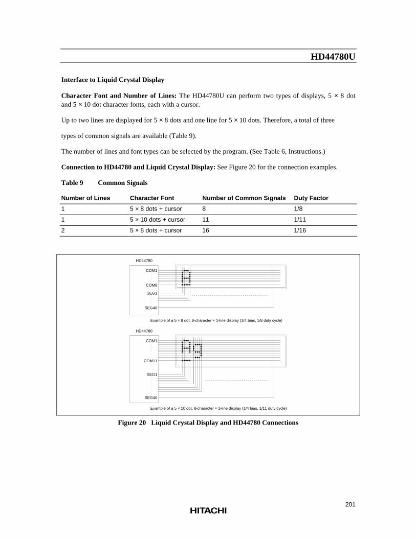
HD44780U
201
Interface to Liquid Crystal Display
Character Font and Number of Lines: The HD44780U can perform two types of displays, 5 × 8 dotand 5 × 10 dot character fonts, each with a cursor.
Up to two lines are displayed for 5 × 8 dots and one line for 5 × 10 dots. Therefore, a total of three
types of common signals are available (Table 9).
The number of lines and font types can be selected by the program. (See Table 6, Instructions.)
Connection to HD44780 and Liquid Crystal Display: See Figure 20 for the connection examples.
Table 9 Common Signals
Number of Lines Character Font Number of Common Signals Duty Factor
1 5 × 8 dots + cursor 8 1/8
1 5 × 10 dots + cursor 11 1/11
2 5 × 8 dots + cursor 16 1/16
COM1
COM8
SEG1
SEG40
COM1
COM11
SEG1
SEG40
HD44780
Example of a 5 × 8 dot, 8-character × 1-line display (1/4 bias, 1/8 duty cycle)
Example of a 5 × 10 dot, 8-character × 1-line display (1/4 bias, 1/11 duty cycle)
HD44780
Figure 20 Liquid Crystal Display and HD44780 Connections
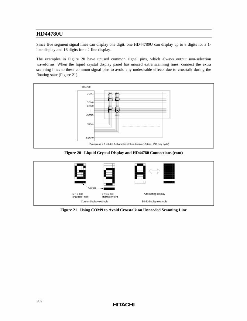
HD44780U
202
Since five segment signal lines can display one digit, one HD44780U can display up to 8 digits for a 1-line display and 16 digits for a 2-line display.
The examples in Figure 20 have unused common signal pins, which always output non-selectionwaveforms. When the liquid crystal display panel has unused extra scanning lines, connect the extrascanning lines to these common signal pins to avoid any undesirable effects due to crosstalk during thefloating state (Figure 21).
COM1
COM8
SEG1
SEG40
HD44780
COM9
COM16
Example of a 5 × 8 dot, 8-character × 2-line display (1/5 bias, 1/16 duty cycle)
Figure 20 Liquid Crystal Display and HD44780 Connections (cont)
Cursor
5 8 dot character font
5 10 dot character font
× × Alternating display
Blink display exampleCursor display example
Figure 21 Using COM9 to Avoid Crosstalk on Unneeded Scanning Line
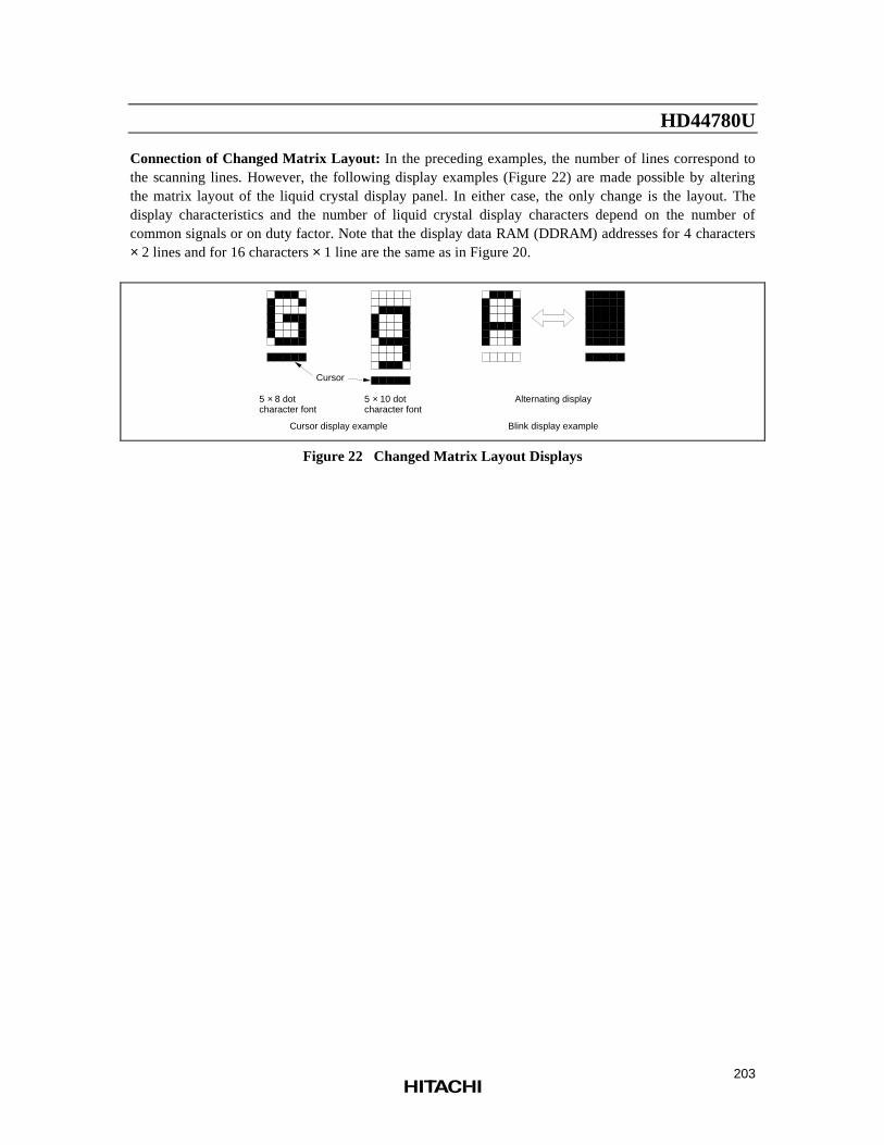
HD44780U
203
Connection of Changed Matrix Layout: In the preceding examples, the number of lines correspond tothe scanning lines. However, the following display examples (Figure 22) are made possible by alteringthe matrix layout of the liquid crystal display panel. In either case, the only change is the layout. Thedisplay characteristics and the number of liquid crystal display characters depend on the number ofcommon signals or on duty factor. Note that the display data RAM (DDRAM) addresses for 4 characters× 2 lines and for 16 characters × 1 line are the same as in Figure 20.
Cursor
5 8 dot character font
5 10 dot character font
× × Alternating display
Blink display exampleCursor display example
Figure 22 Changed Matrix Layout Displays
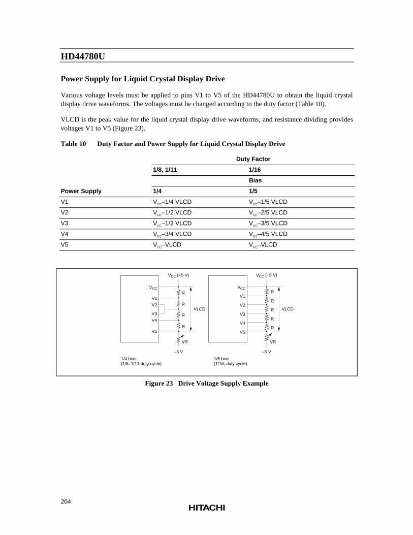
HD44780U
204
Power Supply for Liquid Crystal Display Drive
Various voltage levels must be applied to pins V1 to V5 of the HD44780U to obtain the liquid crystaldisplay drive waveforms. The voltages must be changed according to the duty factor (Table 10).
VLCD is the peak value for the liquid crystal display drive waveforms, and resistance dividing providesvoltages V1 to V5 (Figure 23).
Table 10 Duty Factor and Power Supply for Liquid Crystal Display Drive
Duty Factor
1/8, 1/11 1/16
Bias
Power Supply 1/4 1/5
V1 VCC–1/4 VLCD VCC–1/5 VLCD
V2 VCC–1/2 VLCD VCC–2/5 VLCD
V3 VCC–1/2 VLCD VCC–3/5 VLCD
V4 VCC–3/4 VLCD VCC–4/5 VLCD
V5 VCC–VLCD VCC–VLCD
VCC
V1
V4
V5
V2
V3
VCC
V1
V2
V3
V4
V5
R
R
R
R
VR
–5 V
VCC (+5 V)
–5 V
VCC (+5 V)
R
R
R
R
R
VR
VLCDVLCD
1/4 bias (1/8, 1/11 duty cycle)
1/5 bias (1/16, duty cycle)
Figure 23 Drive Voltage Supply Example
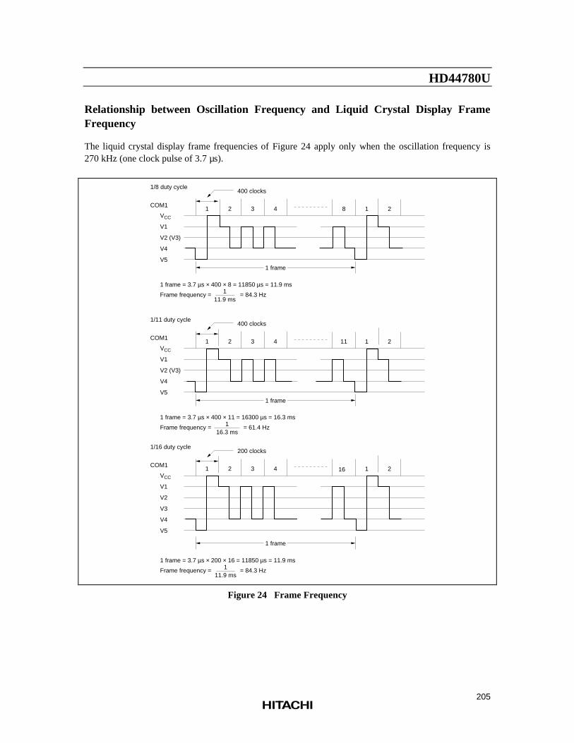
HD44780U
205
Relationship between Oscillation Frequency and Liquid Crystal Display FrameFrequency
The liquid crystal display frame frequencies of Figure 24 apply only when the oscillation frequency is270 kHz (one clock pulse of 3.7 µs).
1 2 3 4 8 1 2
1 2 3 4 11 1 2
1 2 3 4 16 1 2
400 clocks
400 clocks
200 clocks
1 frame
1 frame
1 frame
1/8 duty cycle
1/11 duty cycle
1/16 duty cycle
VCC
V1
V2 (V3)
V4
V5
VCC
V1
V2 (V3)
V4
V5
VCC
V1
V2
V3
V4
V5
COM1
COM1
COM1
1 frame = 3.7 µs × 400 × 8 = 11850 µs = 11.9 ms
Frame frequency = = 84.3 Hz1 11.9 ms
1 frame = 3.7 µs × 400 × 11 = 16300 µs = 16.3 ms
Frame frequency = = 61.4 Hz1 16.3 ms
1 frame = 3.7 µs × 200 × 16 = 11850 µs = 11.9 ms
Frame frequency = = 84.3 Hz1 11.9 ms
Figure 24 Frame Frequency
HD44780U
206
Instruction and Display Correspondence
• 8-bit operation, 8-digit × 1-line display with internal reset
Refer to Table 11 for an example of an 8-digit × 1-line display in 8-bit operation. The HD44780Ufunctions must be set by the function set instruction prior to the display. Since the display data RAMcan store data for 80 characters, as explained before, the RAM can be used for displays such as foradvertising when combined with the display shift operation.
Since the display shift operation changes only the display position with DDRAM contents unchanged,the first display data entered into DDRAM can be output when the return home operation isperformed.
• 4-bit operation, 8-digit × 1-line display with internal reset
The program must set all functions prior to the 4-bit operation (Table 12). When the power is turnedon, 8-bit operation is automatically selected and the first write is performed as an 8-bit operation.Since DB0 to DB3 are not connected, a rewrite is then required. However, since one operation iscompleted in two accesses for 4-bit operation, a rewrite is needed to set the functions (see Table 12).Thus, DB4 to DB7 of the function set instruction is written twice.
• 8-bit operation, 8-digit × 2-line display
For a 2-line display, the cursor automatically moves from the first to the second line after the 40thdigit of the first line has been written. Thus, if there are only 8 characters in the first line, theDDRAM address must be again set after the 8th character is completed. (See Table 13.) Note that thedisplay shift operation is performed for the first and second lines. In the example of Table 13, thedisplay shift is performed when the cursor is on the second line. However, if the shift operation isperformed when the cursor is on the first line, both the first and second lines move together. If theshift is repeated, the display of the second line will not move to the first line. The same display willonly shift within its own line for the number of times the shift is repeated.
Note: When using the internal reset, the electrical characteristics in the Power Supply Conditions UsingInternal Reset Circuit table must be satisfied. If not, the HD44780U must be initialized byinstructions. See the section, Initializing by Instruction.
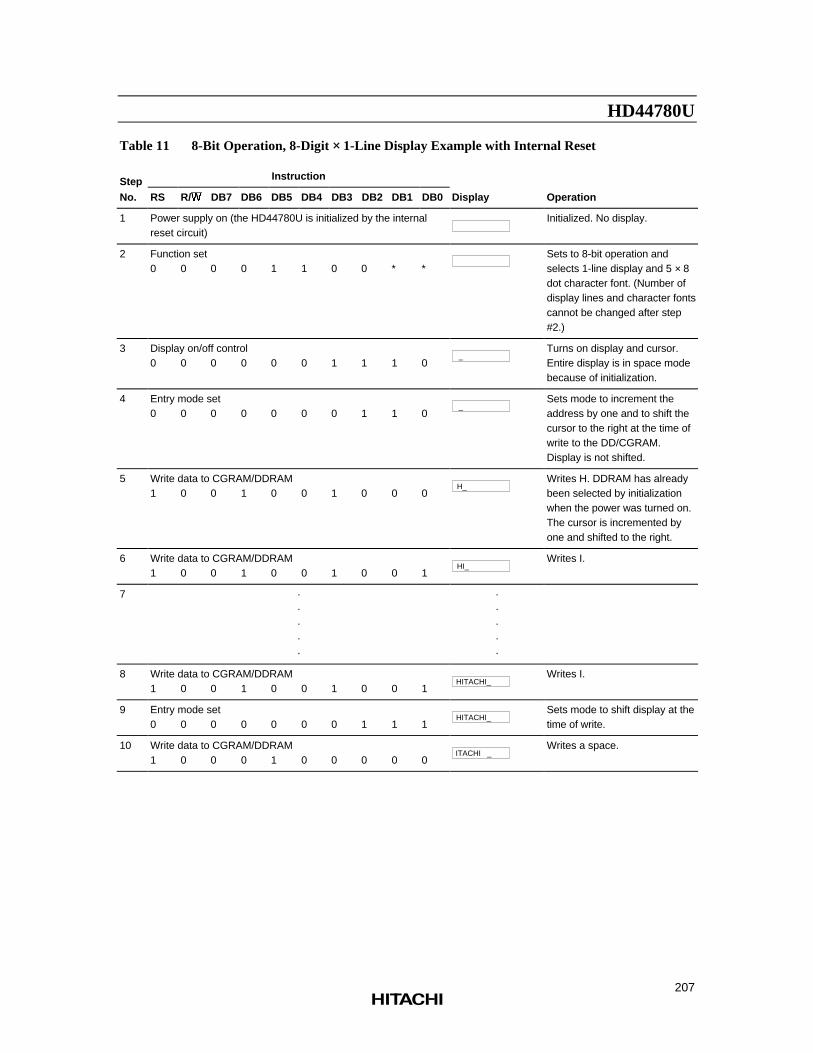
HD44780U
207
Table 11 8-Bit Operation, 8-Digit ×× 1-Line Display Example with Internal Reset
Step Instruction
No. RS R/:: DB7 DB6 DB5 DB4 DB3 DB2 DB1 DB0 Display Operation
1 Power supply on (the HD44780U is initialized by the internalreset circuit)
Initialized. No display.
2 Function set0 0 0 0 1 1 0 0 * *
Sets to 8-bit operation andselects 1-line display and 5 × 8dot character font. (Number ofdisplay lines and character fontscannot be changed after step#2.)
3 Display on/off control0 0 0 0 0 0 1 1 1 0
_ Turns on display and cursor.Entire display is in space modebecause of initialization.
4 Entry mode set0 0 0 0 0 0 0 1 1 0
_ Sets mode to increment theaddress by one and to shift thecursor to the right at the time ofwrite to the DD/CGRAM.Display is not shifted.
5 Write data to CGRAM/DDRAM1 0 0 1 0 0 1 0 0 0
H_ Writes H. DDRAM has alreadybeen selected by initializationwhen the power was turned on.The cursor is incremented byone and shifted to the right.
6 Write data to CGRAM/DDRAM1 0 0 1 0 0 1 0 0 1
HI_ Writes I.
7 ·····
·····
8 Write data to CGRAM/DDRAM1 0 0 1 0 0 1 0 0 1
HITACHI_ Writes I.
9 Entry mode set0 0 0 0 0 0 0 1 1 1
HITACHI_ Sets mode to shift display at thetime of write.
10 Write data to CGRAM/DDRAM1 0 0 0 1 0 0 0 0 0
ITACHI _ Writes a space.
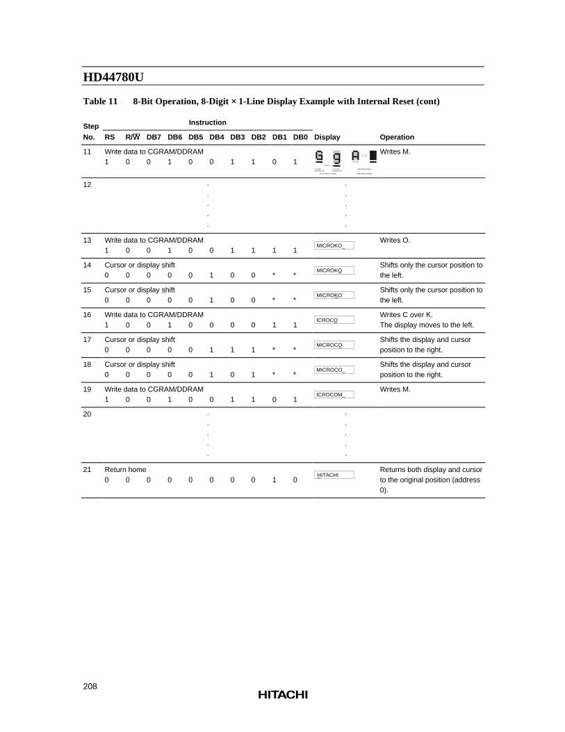
HD44780U
208
Table 11 8-Bit Operation, 8-Digit ×× 1-Line Display Example with Internal Reset (cont)
Step Instruction
No. RS R/:: DB7 DB6 DB5 DB4 DB3 DB2 DB1 DB0 Display Operation
11 Write data to CGRAM/DDRAM1 0 0 1 0 0 1 1 0 1
Cursor
5 8 dot character font
5 10 dot character font
× × Alternating display
Blink display exampleCursor display example
Writes M.
12 ·····
·····
13 Write data to CGRAM/DDRAM1 0 0 1 0 0 1 1 1 1
MICROKO_ Writes O.
14 Cursor or display shift0 0 0 0 0 1 0 0 * *
MICROKO _Shifts only the cursor position tothe left.
15 Cursor or display shift0 0 0 0 0 1 0 0 * *
MICROKO _Shifts only the cursor position tothe left.
16 Write data to CGRAM/DDRAM1 0 0 1 0 0 0 0 1 1
ICROCO _Writes C over K.The display moves to the left.
17 Cursor or display shift0 0 0 0 0 1 1 1 * *
MICROCO _Shifts the display and cursorposition to the right.
18 Cursor or display shift0 0 0 0 0 1 0 1 * *
MICROCO_ Shifts the display and cursorposition to the right.
19 Write data to CGRAM/DDRAM1 0 0 1 0 0 1 1 0 1
ICROCOM_ Writes M.
20 ·····
·····
21 Return home0 0 0 0 0 0 0 0 1 0
HITACHI _ Returns both display and cursorto the original position (address0).
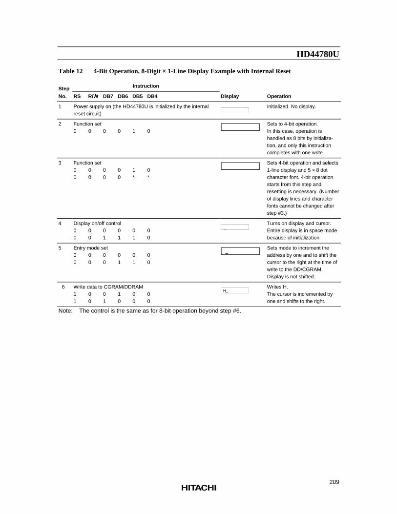
HD44780U
209
Table 12 4-Bit Operation, 8-Digit ×× 1-Line Display Example with Internal Reset
Step Instruction
No. RS R/:: DB7 DB6 DB5 DB4 Display Operation
1 Power supply on (the HD44780U is initialized by the internalreset circuit)
Initialized. No display.
2 Function set0 0 0 0 1 0
Sets to 4-bit operation.In this case, operation ishandled as 8 bits by initializa-tion, and only this instructioncompletes with one write.
3 Function set0 0 0 0 1 00 0 0 0 * *
Sets 4-bit operation and selects1-line display and 5 × 8 dotcharacter font. 4-bit operationstarts from this step andresetting is necessary. (Numberof display lines and characterfonts cannot be changed afterstep #3.)
4 Display on/off control0 0 0 0 0 00 0 1 1 1 0
_ Turns on display and cursor.Entire display is in space modebecause of initialization.
5 Entry mode set0 0 0 0 0 00 0 0 1 1 0
Sets mode to increment theaddress by one and to shift thecursor to the right at the time ofwrite to the DD/CGRAM.Display is not shifted.
6 Write data to CGRAM/DDRAM1 0 0 1 0 01 0 1 0 0 0
H_ Writes H.The cursor is incremented byone and shifts to the right.
Note: The control is the same as for 8-bit operation beyond step #6.
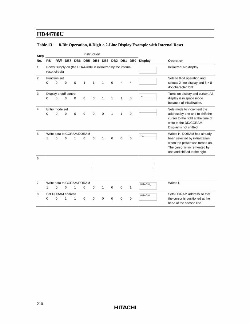
HD44780U
210
Table 13 8-Bit Operation, 8-Digit ×× 2-Line Display Example with Internal Reset
Step Instruction
No. RS R/:: DB7 DB6 DB5 DB4 DB3 DB2 DB1 DB0 Display Operation
1 Power supply on (the HD44780U is initialized by the internalreset circuit)
Initialized. No display.
2 Function set0 0 0 0 1 1 1 0 * *
Sets to 8-bit operation andselects 2-line display and 5 × 8dot character font.
3 Display on/off control0 0 0 0 0 0 1 1 1 0
_ Turns on display and cursor. Alldisplay is in space modebecause of initialization.
4 Entry mode set0 0 0 0 0 0 0 1 1 0
_ Sets mode to increment theaddress by one and to shift thecursor to the right at the time ofwrite to the DD/CGRAM.Display is not shifted.
5 Write data to CGRAM/DDRAM1 0 0 1 0 0 1 0 0 0
H_ Writes H. DDRAM has alreadybeen selected by initializationwhen the power was turned on.The cursor is incremented byone and shifted to the right.
6 ·····
·····
7 Write data to CGRAM/DDRAM1 0 0 1 0 0 1 0 0 1
HITACHI_ Writes I.
8 Set DDRAM address0 0 1 1 0 0 0 0 0 0
HITACHI _
Sets DDRAM address so thatthe cursor is positioned at thehead of the second line.
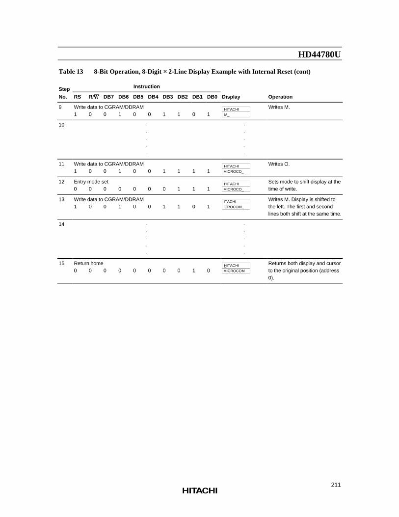
HD44780U
211
Table 13 8-Bit Operation, 8-Digit ×× 2-Line Display Example with Internal Reset (cont)
Step Instruction
No. RS R/:: DB7 DB6 DB5 DB4 DB3 DB2 DB1 DB0 Display Operation
9 Write data to CGRAM/DDRAM1 0 0 1 0 0 1 1 0 1
HITACHI M_
Writes M.
10 ·····
·····
11 Write data to CGRAM/DDRAM1 0 0 1 0 0 1 1 1 1
HITACHI MICROCO_
Writes O.
12 Entry mode set0 0 0 0 0 0 0 1 1 1
HITACHI MICROCO_
Sets mode to shift display at thetime of write.
13 Write data to CGRAM/DDRAM1 0 0 1 0 0 1 1 0 1
ITACHI ICROCOM_
Writes M. Display is shifted tothe left. The first and secondlines both shift at the same time.
14 ·····
·····
15 Return home0 0 0 0 0 0 0 0 1 0
HITACHI MICROCOM _ Returns both display and cursor
to the original position (address0).
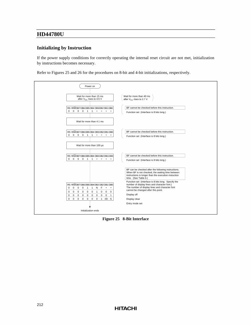
HD44780U
212
Initializing by Instruction
If the power supply conditions for correctly operating the internal reset circuit are not met, initializationby instructions becomes necessary.
Refer to Figures 25 and 26 for the procedures on 8-bit and 4-bit initializations, respectively.
Power on
Wait for more than 15 ms after VCC rises to 4.5 V
Wait for more than 4.1 ms
Wait for more than 100 µs
RS 0
R/W 0
DB7 0
DB6 0
DB5 1
DB4 1
DB3DB2 DB1 DB0 * * * *
RS 0
R/W 0
DB7 0
DB6 0
DB5 1
DB4 1
DB3DB2DB1DB0* * * *
RS 0
R/W 0
DB7 0
DB6 0
DB5 1
DB4 1
DB3DB2DB1* * *
DB0*
RS 0
R/W 0
DB7 0
DB6 0
DB5 1
DB4 1
DB3 N
DB2 F
DB1DB0* *
0
0
0
0
0
0
0
0
0
0
0
0
0
0
0
0
0
0
1
0
0
0
0
1
0
0
I/D
0
1
S
Initialization ends
BF cannot be checked before this instruction.
Function set (Interface is 8 bits long.)
BF cannot be checked before this instruction.
Function set (Interface is 8 bits long.)
BF cannot be checked before this instruction.
Function set (Interface is 8 bits long.)
BF can be checked after the following instructions. When BF is not checked, the waiting time between instructions is longer than the execution instuction time. (See Table 6.)
Function set (Interface is 8 bits long. Specify the number of display lines and character font.) The number of display lines and character font cannot be changed after this point.
Display off
Display clear
Entry mode set
Wait for more than 40 ms after VCC rises to 2.7 V
Figure 25 8-Bit Interface
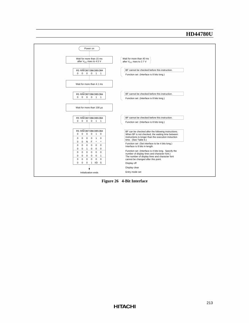
HD44780U
213
Initialization ends
Wait for more than 15 ms after VCC rises to 4.5 V
Wait for more than 40 ms after VCC rises to 2.7 V
BF cannot be checked before this instruction.
Function set (Interface is 8 bits long.)
BF cannot be checked before this instruction.
Function set (Interface is 8 bits long.)
BF cannot be checked before this instruction.
Function set (Interface is 8 bits long.)
DB7 0
DB6 0
DB5 1
DB4 1
RS 0
R/W 0
Wait for more than 4.1 ms
DB7 0
DB6 0
DB5 1
DB4 1
RS 0
R/W 0
Wait for more than 100 µs
DB7 0
DB6 0
DB5 1
DB4 1
RS 0
R/W 0
DB7 0
DB6 0
DB5 1
DB4 0
RS 0
R/W 0
0
N
0
1
0
0
0
0
0
F
0
0
0
0
0
1
1
0
0
0
0
0
I/D
0
0
0
0
1
0
S
0
0
0
0
0
0
0
0
0
0
0
0
0
0
0
0
* *
BF can be checked after the following instructions. When BF is not checked, the waiting time between instructions is longer than the execution instuction time. (See Table 6.)
Function set (Set interface to be 4 bits long.) Interface is 8 bits in length.
Display off
Display clear
Entry mode set
Function set (Interface is 4 bits long. Specify the number of display lines and character font.) The number of display lines and character font cannot be changed after this point.
Power on
Figure 26 4-Bit Interface
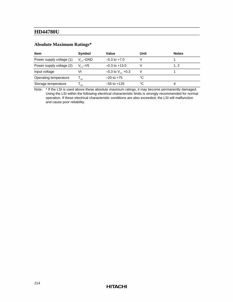
HD44780U
214
Absolute Maximum Ratings*
Item Symbol Value Unit Notes
Power supply voltage (1) VCC–GND –0.3 to +7.0 V 1
Power supply voltage (2) VCC–V5 –0.3 to +13.0 V 1, 2
Input voltage Vt –0.3 to VCC +0.3 V 1
Operating temperature Topr –20 to +75 °C
Storage temperature Tstg –55 to +125 °C 4
Note: * If the LSI is used above these absolute maximum ratings, it may become permanently damaged.Using the LSI within the following electrical characteristic limits is strongly recommended for normaloperation. If these electrical characteristic conditions are also exceeded, the LSI will malfunctionand cause poor reliability.
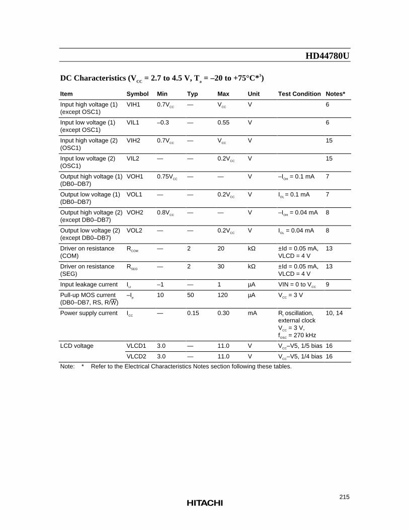
HD44780U
215
DC Characteristics (VCC = 2.7 to 4.5 V, Ta = –20 to +75°C*3)
Item Symbol Min Typ Max Unit Test Condition Notes*
Input high voltage (1)(except OSC1)
VIH1 0.7VCC — VCC V 6
Input low voltage (1)(except OSC1)
VIL1 –0.3 — 0.55 V 6
Input high voltage (2)(OSC1)
VIH2 0.7VCC — VCC V 15
Input low voltage (2)(OSC1)
VIL2 — — 0.2VCC V 15
Output high voltage (1)(DB0–DB7)
VOH1 0.75VCC — — V –IOH = 0.1 mA 7
Output low voltage (1)(DB0–DB7)
VOL1 — — 0.2VCC V IOL = 0.1 mA 7
Output high voltage (2)(except DB0–DB7)
VOH2 0.8VCC — — V –IOH = 0.04 mA 8
Output low voltage (2)(except DB0–DB7)
VOL2 — — 0.2VCC V IOL = 0.04 mA 8
Driver on resistance(COM)
RCOM — 2 20 kΩ ±Id = 0.05 mA,VLCD = 4 V
13
Driver on resistance(SEG)
RSEG — 2 30 kΩ ±Id = 0.05 mA,VLCD = 4 V
13
Input leakage current ILI –1 — 1 µA VIN = 0 to VCC 9
Pull-up MOS current(DB0–DB7, RS, R/:)
–Ip 10 50 120 µA VCC = 3 V
Power supply current ICC — 0.15 0.30 mA Rf oscillation,external clockVCC = 3 V,fOSC = 270 kHz
10, 14
LCD voltage VLCD1 3.0 — 11.0 V VCC–V5, 1/5 bias 16
VLCD2 3.0 — 11.0 V VCC–V5, 1/4 bias 16
Note: * Refer to the Electrical Characteristics Notes section following these tables.
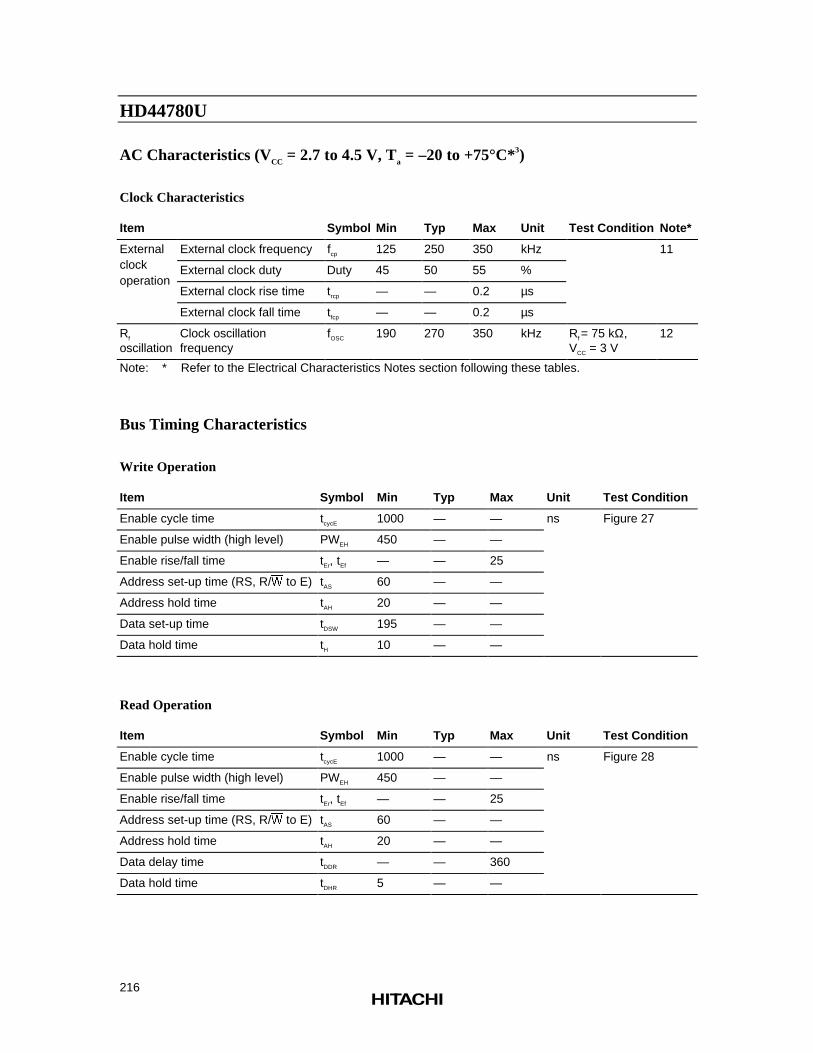
HD44780U
216
AC Characteristics (VCC = 2.7 to 4.5 V, Ta = –20 to +75°C*3)
Clock Characteristics
Item Symbol Min Typ Max Unit Test Condition Note*
External External clock frequency fcp 125 250 350 kHz 11clock External clock duty Duty 45 50 55 %operation
External clock rise time trcp — — 0.2 µs
External clock fall time tfcp — — 0.2 µs
Rf
oscillationClock oscillationfrequency
fOSC 190 270 350 kHz Rf = 75 kΩ,VCC = 3 V
12
Note: * Refer to the Electrical Characteristics Notes section following these tables.
Bus Timing Characteristics
Write Operation
Item Symbol Min Typ Max Unit Test Condition
Enable cycle time tcycE 1000 — — ns Figure 27
Enable pulse width (high level) PWEH 450 — —
Enable rise/fall time tEr, tEf — — 25
Address set-up time (RS, R/: to E) tAS 60 — —
Address hold time tAH 20 — —
Data set-up time tDSW 195 — —
Data hold time tH 10 — —
Read Operation
Item Symbol Min Typ Max Unit Test Condition
Enable cycle time tcycE 1000 — — ns Figure 28
Enable pulse width (high level) PWEH 450 — —
Enable rise/fall time tEr, tEf — — 25
Address set-up time (RS, R/: to E) tAS 60 — —
Address hold time tAH 20 — —
Data delay time tDDR — — 360
Data hold time tDHR 5 — —
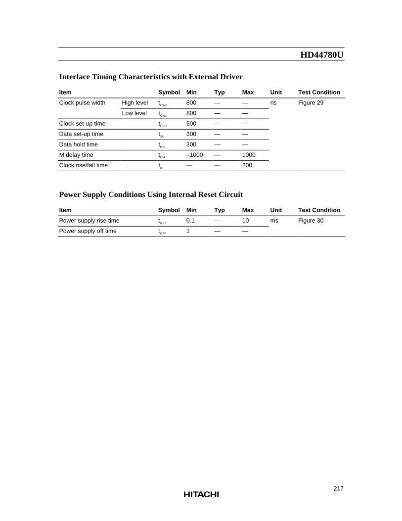
HD44780U
217
Interface Timing Characteristics with External Driver
Item Symbol Min Typ Max Unit Test Condition
Clock pulse width High level tCWH 800 — — ns Figure 29
Low level tCWL 800 — —
Clock set-up time tCSU 500 — —
Data set-up time tSU 300 — —
Data hold time tDH 300 — —
M delay time tDM –1000 — 1000
Clock rise/fall time tct — — 200
Power Supply Conditions Using Internal Reset Circuit
Item Symbol Min Typ Max Unit Test Condition
Power supply rise time trCC 0.1 — 10 ms Figure 30
Power supply off time tOFF 1 — —
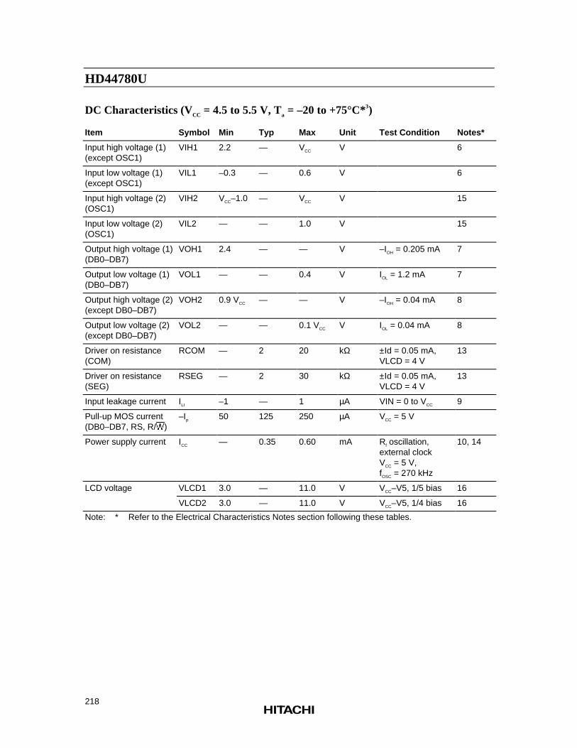
HD44780U
218
DC Characteristics (VCC = 4.5 to 5.5 V, Ta = –20 to +75°C*3)
Item Symbol Min Typ Max Unit Test Condition Notes*
Input high voltage (1)(except OSC1)
VIH1 2.2 — VCC V 6
Input low voltage (1)(except OSC1)
VIL1 –0.3 — 0.6 V 6
Input high voltage (2)(OSC1)
VIH2 VCC–1.0 — VCC V 15
Input low voltage (2)(OSC1)
VIL2 — — 1.0 V 15
Output high voltage (1)(DB0–DB7)
VOH1 2.4 — — V –IOH = 0.205 mA 7
Output low voltage (1)(DB0–DB7)
VOL1 — — 0.4 V IOL = 1.2 mA 7
Output high voltage (2)(except DB0–DB7)
VOH2 0.9 VCC — — V –IOH = 0.04 mA 8
Output low voltage (2)(except DB0–DB7)
VOL2 — — 0.1 VCC V IOL = 0.04 mA 8
Driver on resistance(COM)
RCOM — 2 20 kΩ ±Id = 0.05 mA,VLCD = 4 V
13
Driver on resistance(SEG)
RSEG — 2 30 kΩ ±Id = 0.05 mA,VLCD = 4 V
13
Input leakage current ILI –1 — 1 µA VIN = 0 to VCC 9
Pull-up MOS current(DB0–DB7, RS, R/:)
–Ip 50 125 250 µA VCC = 5 V
Power supply current ICC — 0.35 0.60 mA Rf oscillation,external clockVCC = 5 V,fOSC = 270 kHz
10, 14
LCD voltage VLCD1 3.0 — 11.0 V VCC–V5, 1/5 bias 16
VLCD2 3.0 — 11.0 V VCC–V5, 1/4 bias 16
Note: * Refer to the Electrical Characteristics Notes section following these tables.
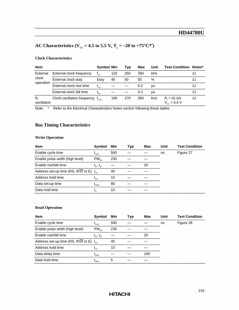
HD44780U
219
AC Characteristics (VCC = 4.5 to 5.5 V, Ta = –20 to +75°C*3)
Clock Characteristics
Item Symbol Min Typ Max Unit Test Condition Notes*
External External clock frequency fcp 125 250 350 kHz 11clock External clock duty Duty 45 50 55 % 11operation
External clock rise time trcp — — 0.2 µs 11
External clock fall time tfcp — — 0.2 µs 11
Rf
oscillationClock oscillation frequency fOSC 190 270 350 kHz Rf = 91 kΩ
VCC = 5.0 V12
Note: * Refer to the Electrical Characteristics Notes section following these tables.
Bus Timing Characteristics
Write Operation
Item Symbol Min Typ Max Unit Test Condition
Enable cycle time tcycE 500 — — ns Figure 27
Enable pulse width (high level) PWEH 230 — —
Enable rise/fall time tEr, tEf — — 20
Address set-up time (RS, R/: to E) tAS 40 — —
Address hold time tAH 10 — —
Data set-up time tDSW 80 — —
Data hold time tH 10 — —
Read Operation
Item Symbol Min Typ Max Unit Test Condition
Enable cycle time tcycE 500 — — ns Figure 28
Enable pulse width (high level) PWEH 230 — —
Enable rise/fall time tEr, tEf — — 20
Address set-up time (RS, R/: to E) tAS 40 — —
Address hold time tAH 10 — —
Data delay time tDDR — — 160
Data hold time tDHR 5 — —
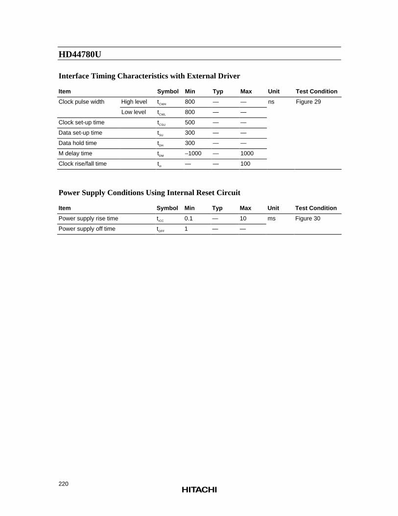
HD44780U
220
Interface Timing Characteristics with External Driver
Item Symbol Min Typ Max Unit Test Condition
Clock pulse width High level tCWH 800 — — ns Figure 29
Low level tCWL 800 — —
Clock set-up time tCSU 500 — —
Data set-up time tSU 300 — —
Data hold time tDH 300 — —
M delay time tDM –1000 — 1000
Clock rise/fall time tct — — 100
Power Supply Conditions Using Internal Reset Circuit
Item Symbol Min Typ Max Unit Test Condition
Power supply rise time trCC 0.1 — 10 ms Figure 30
Power supply off time tOFF 1 — —
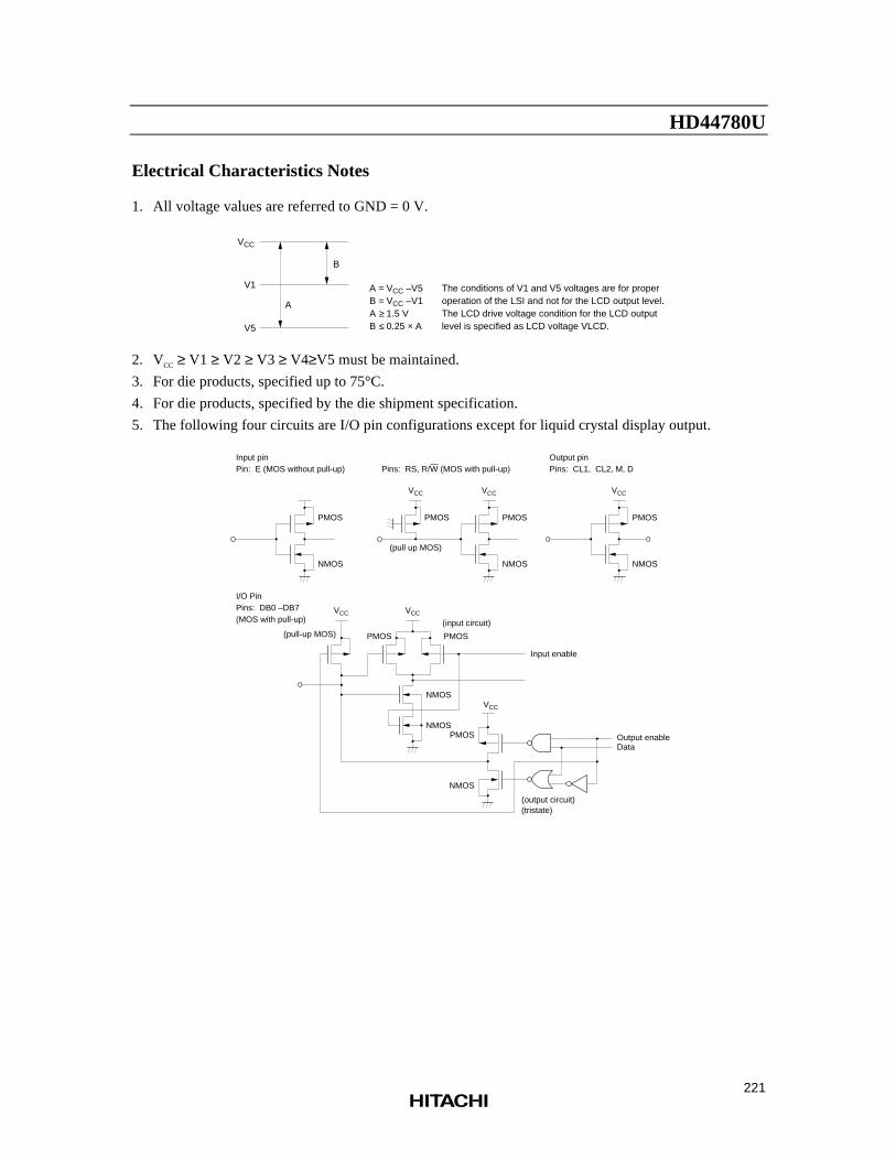
HD44780U
221
Electrical Characteristics Notes
1. All voltage values are referred to GND = 0 V.
VCC
A
B
A 1.5 V B 0.25 × A
≥ ≤
The conditions of V1 and V5 voltages are for proper operation of the LSI and not for the LCD output level. The LCD drive voltage condition for the LCD output level is specified as LCD voltage VLCD.
A = B =
VCC –V5 VCC –V1
V1
V5
2. VCC ≥ V1 ≥ V2 ≥ V3 ≥ V4≥V5 must be maintained.
3. For die products, specified up to 75°C.
4. For die products, specified by the die shipment specification.
5. The following four circuits are I/O pin configurations except for liquid crystal display output.
PMOS
NMOS
VCC VCC
PMOS
NMOS
(pull up MOS)
PMOS
VCC
PMOS
NMOS
VCC
NMOS
NMOS
VCC
PMOS
NMOS
(output circuit) (tristate)
Output enable Data
(pull-up MOS)
I/O Pin Pins: DB0 –DB7 (MOS with pull-up)
Input pin Pin: E (MOS without pull-up)
Pins: RS, R/W (MOS with pull-up)
Output pin Pins: CL1, CL2, M, D
VCC
(input circuit)
PMOSPMOS
Input enable
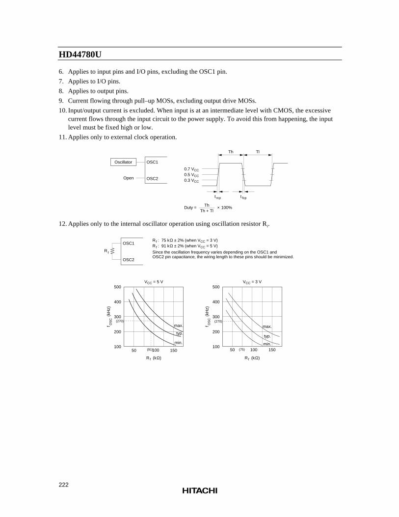
HD44780U
222
6. Applies to input pins and I/O pins, excluding the OSC1 pin.
7. Applies to I/O pins.
8. Applies to output pins.
9. Current flowing through pull–up MOSs, excluding output drive MOSs.
10. Input/output current is excluded. When input is at an intermediate level with CMOS, the excessivecurrent flows through the input circuit to the power supply. To avoid this from happening, the inputlevel must be fixed high or low.
11. Applies only to external clock operation.
Oscillator OSC1
OSC2
0.7 VCC 0.5 VCC 0.3 VCC
Th Tl
t rcp t fcp
Duty = 100%Th Th + Tl
×
Open
12. Applies only to the internal oscillator operation using oscillation resistor Rf.
OSC1
OSC2
Rf
R : R :
f
f
75 k ± 2% (when VCC = 3 V) 91 k ± 2% (when VCC = 5 V)Ω
500
400
300
200
10050 100 150(91)
R (k )f Ω
f
(k
Hz)
OS
C
VCC = 5 V500
400
300
200
10050 100 150
R (k )f Ω
f
(k
Hz)
OS
C
VCC = 3 V
typ.
Since the oscillation frequency varies depending on the OSC1 and OSC2 pin capacitance, the wiring length to these pins should be minimized.
(270) (270)
Ω
(75)
typ.
max.
min.
max.
min.
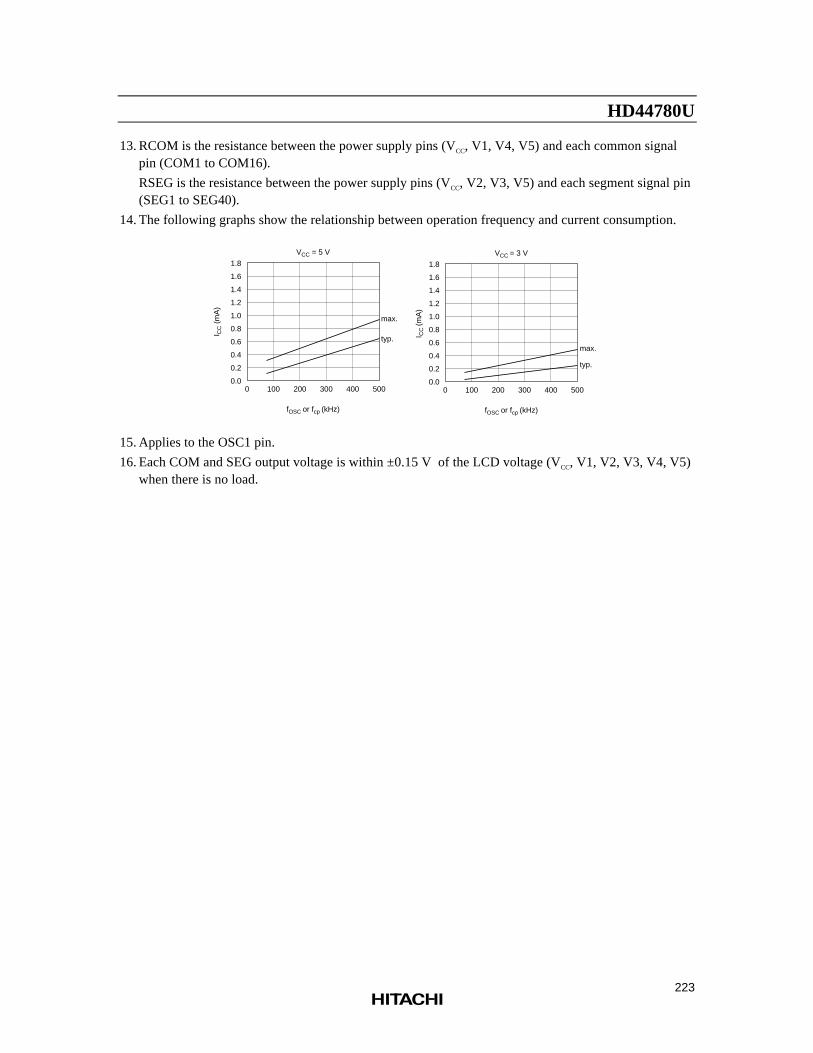
HD44780U
223
13. RCOM is the resistance between the power supply pins (VCC, V1, V4, V5) and each common signalpin (COM1 to COM16).
RSEG is the resistance between the power supply pins (VCC, V2, V3, V5) and each segment signal pin(SEG1 to SEG40).
14. The following graphs show the relationship between operation frequency and current consumption.
1.8
1.6
1.4
1.2
1.0
0.8
0.6
0.4
0.2
0.0
1.8
1.6
1.4
1.2
1.0
0.8
0.6
0.4
0.2
0.00 100 200 300 400 500
VCC = 5 V
0 100 200 300 400 500
VCC = 3 V
fOSC or fcp (kHz) fOSC or fcp (kHz)
I CC (
mA
)
I CC
(mA
)
max.
typ.max.
typ.
15. Applies to the OSC1 pin.
16. Each COM and SEG output voltage is within ±0.15 V of the LCD voltage (VCC, V1, V2, V3, V4, V5)when there is no load.
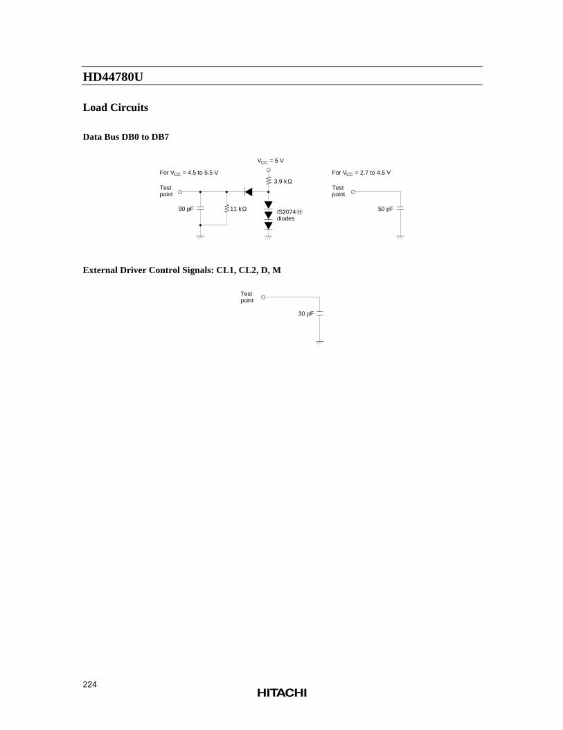
HD44780U
224
Load Circuits
Data Bus DB0 to DB7
For V = 4.5 to 5.5 VCC
Testpoint
90 pF 11 kΩ
V = 5 VCC
3.9 kΩ
IS2074diodes
H
For V = 2.7 to 4.5 VCC
Testpoint
50 pF
External Driver Control Signals: CL1, CL2, D, M
Test point
30 pF
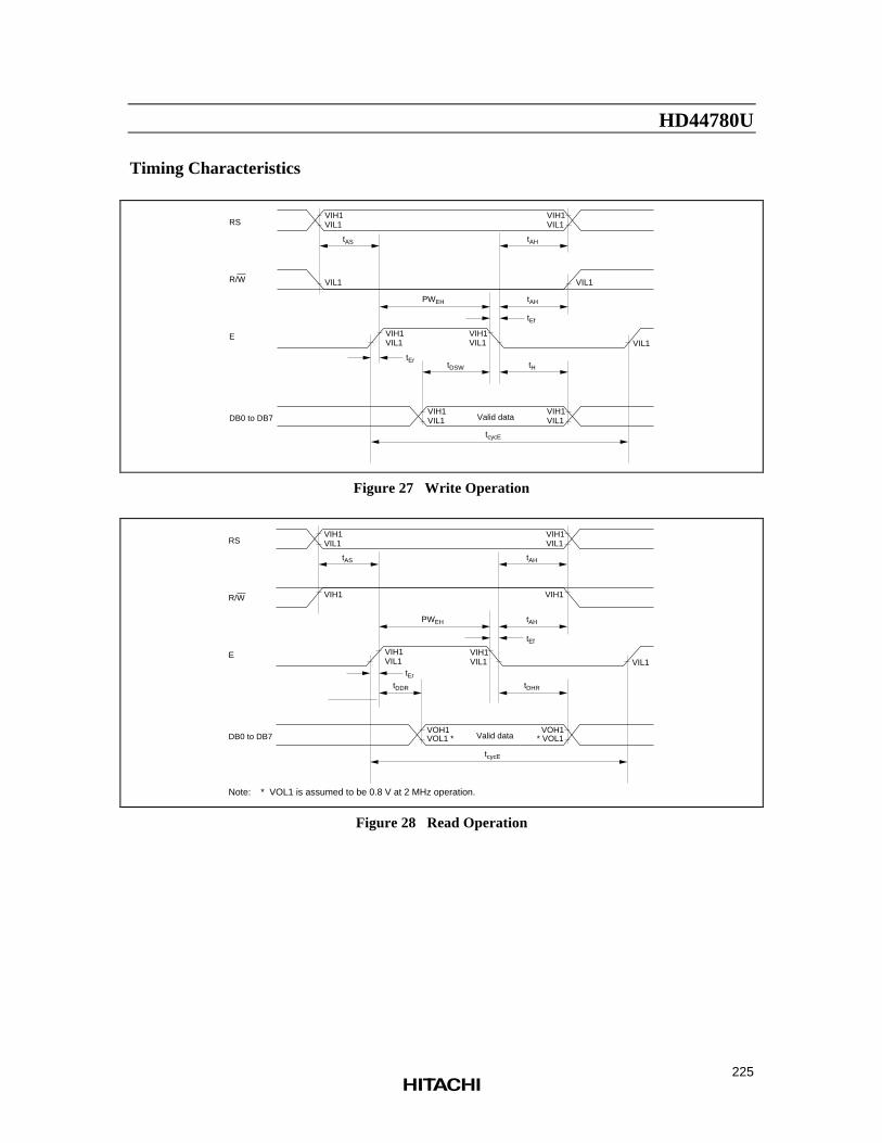
HD44780U
225
Timing Characteristics
RS
R/W
E
DB0 to DB7
VIH1 VIL1
VIH1 VIL1
tAS tAH
VIL1 VIL1
tAHPWEH
tEf
VIH1 VIL1
VIH1 VIL1
tErtDSW tH
VIH1 VIL1
VIH1 VIL1
tcycE
VIL1
Valid data
Figure 27 Write Operation
RS
R/W
E
DB0 to DB7
VIH1 VIL1
VIH1 VIL1
tAS tAH
VIH1 VIH1
tAHPWEH
tEf
VIH1 VIL1
VIH1 VIL1
tDDR tDHR
tEr
VIL1
VOH1 VOL1 *
VOH1 * VOL1Valid data
tcycE
Note: * VOL1 is assumed to be 0.8 V at 2 MHz operation.
Figure 28 Read Operation
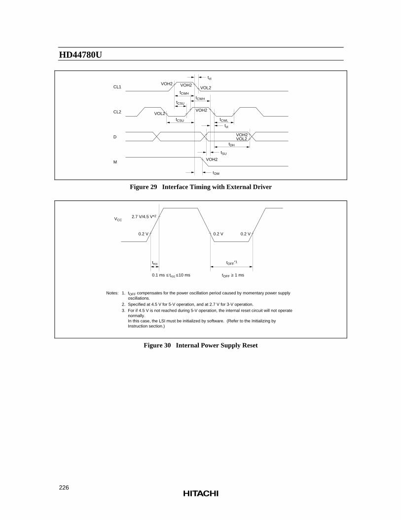
HD44780U
226
CL1
CL2
D
M
VOH2 VOH2VOL2
tct
tCWH
tCWH
tCSU
VOH2
tCSU tCWL
tct
tDH
tSU
VOH2
tDM
VOH2 VOL2
VOL2
Figure 29 Interface Timing with External Driver
VCC
0.2 V
2.7 V/4.5 V*2
0.2 V 0.2 V
trcc tOFF*1
0.1 ms trcc 10 ms≤ ≤ tOFF 1 ms≥
Notes: 1. 2. 3.
tOFF compensates for the power oscillation period caused by momentary power supply oscillations. Specified at 4.5 V for 5-V operation, and at 2.7 V for 3-V operation. For if 4.5 V is not reached during 5-V operation, the internal reset circuit will not operate normally. In this case, the LSI must be initialized by software. (Refer to the Initializing by Instruction section.)
Figure 30 Internal Power Supply Reset
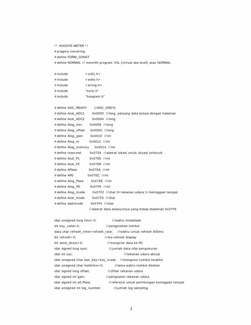
1
/* HOOGTE METER */
#pragma romstring
#define FORM_CONST
#define NORMAL // memilih program VSL (virtual sea level) atau NORMAL
#include <cc51.h>
#include <stdio.h>
#include <string.h>
#include "extio.h"
#include "hoogtem.h"
#define ADC_READY (!ADC_DRDY)
#define Acal_ADC1 0x0000 //long, panjang data sesuai dengan halaman
#define Acal_ADC2 0x0004 //long
#define Alog_intv 0x0008 //long
#define Alog_offset 0x000C //long
#define Alog_gain 0x0010 //int
#define Alog_nr 0x0012 //int
#define Alog_memory 0x0014 //int
#define reserved 0x07E4 //alamat lokasi untuk situasi terburuk
#define Acal_P1 0x07E6 //int
#define Acal_P2 0x07E8 //int
#define APsea 0x07EA //int
#define AP0 0x07EC //int
#define Alog_Psea 0x07EE //int
#define Alog_P0 0x07F0 //int
#define Alog_mode 0x07F2 //char 0=tekanan udara 1=ketinggian tempat
#define Acal_mode 0x07F3 //char
#define Aaltimode 0x07F4 //char
//alamat data selanjutnya yang bebas dialamati 0x07F5
idat unsigned long time=0; //waktu inisialisasi
bit key_valid=0; //pengecekan tombol
data char refresh_time=refresh_rate; //waktu untuk refresh 400ms
bit refresh=0; //me-refresh display
bit send_direct=0; //mengirim data ke PC
idat signed long sum; //jumlah data nilai pengukuran
idat int out; //tekanan udara aktual
idat unsigned char last_key=key_mask; //mengunci tombol terakhir
idat unsigned char holdtime=0; //lama waktu tombol ditekan
idat signed long offset; //offset tekanan udara
idat signed int gain; //penguatan tekanan udara
idat signed int p0,Psea; //referensi untuk perhitungan ketinggian tempat
idat unsigned int log_number; //jumlah log sampling
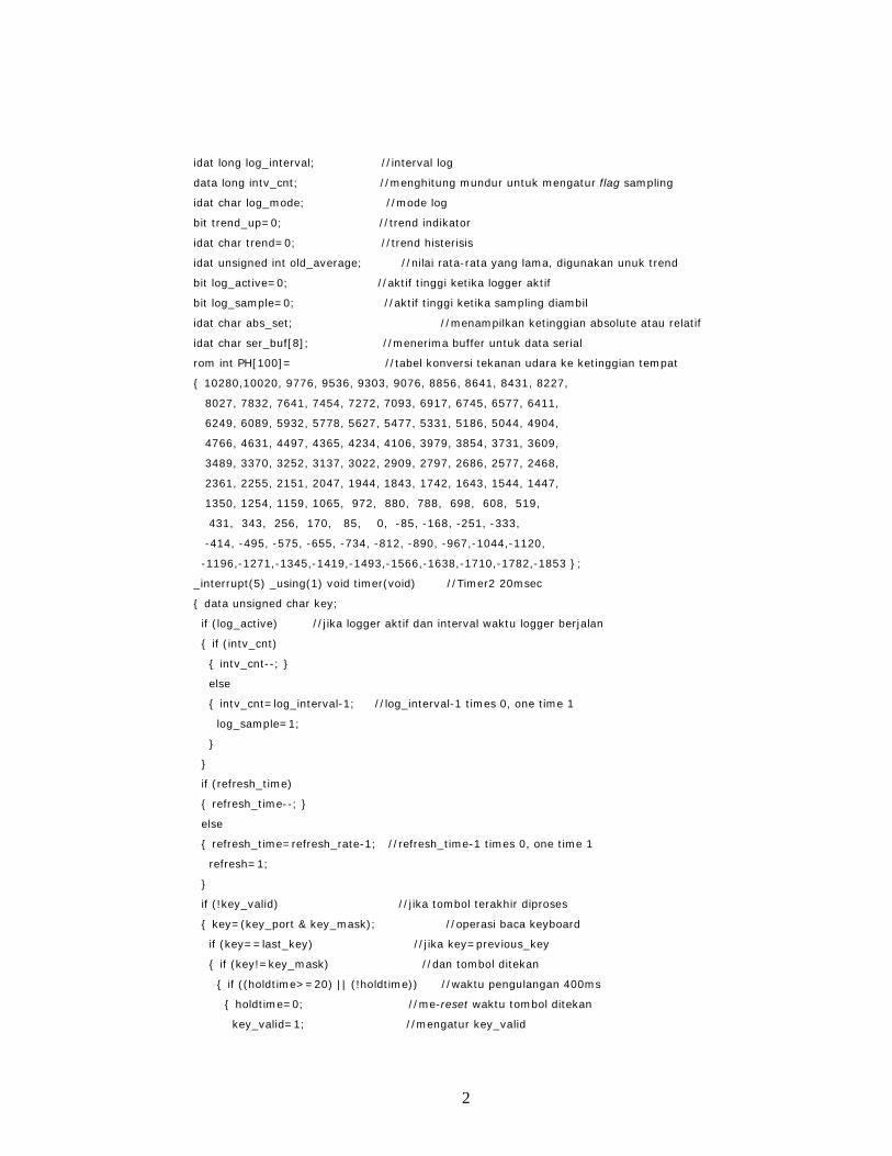
2
idat long log_interval; //interval log
data long intv_cnt; //menghitung mundur untuk mengatur flag sampling
idat char log_mode; //mode log
bit trend_up=0; //trend indikator
idat char trend=0; //trend histerisis
idat unsigned int old_average; //nilai rata-rata yang lama, digunakan unuk trend
bit log_active=0; //aktif tinggi ketika logger aktif
bit log_sample=0; //aktif tinggi ketika sampling diambil
idat char abs_set; //menampilkan ketinggian absolute atau relatif
idat char ser_buf[8]; //menerima buffer untuk data serial
rom int PH[100]= //tabel konversi tekanan udara ke ketinggian tempat
10280,10020, 9776, 9536, 9303, 9076, 8856, 8641, 8431, 8227,
8027, 7832, 7641, 7454, 7272, 7093, 6917, 6745, 6577, 6411,
6249, 6089, 5932, 5778, 5627, 5477, 5331, 5186, 5044, 4904,
4766, 4631, 4497, 4365, 4234, 4106, 3979, 3854, 3731, 3609,
3489, 3370, 3252, 3137, 3022, 2909, 2797, 2686, 2577, 2468,
2361, 2255, 2151, 2047, 1944, 1843, 1742, 1643, 1544, 1447,
1350, 1254, 1159, 1065, 972, 880, 788, 698, 608, 519,
431, 343, 256, 170, 85, 0, -85, -168, -251, -333,
-414, -495, -575, -655, -734, -812, -890, -967,-1044,-1120,
-1196,-1271,-1345,-1419,-1493,-1566,-1638,-1710,-1782,-1853 ;
_interrupt(5) _using(1) void timer(void) //Timer2 20msec
data unsigned char key;
if (log_active) //jika logger aktif dan interval waktu logger berjalan
if (intv_cnt)
intv_cnt--;
else
intv_cnt=log_interval-1; //log_interval-1 times 0, one time 1
log_sample=1;
if (refresh_time)
refresh_time--;
else
refresh_time=refresh_rate-1; //refresh_time-1 times 0, one time 1
refresh=1;
if (!key_valid) //jika tombol terakhir diproses
key=(key_port & key_mask); //operasi baca keyboard
if (key==last_key) //jika key=previous_key
if (key!=key_mask) //dan tombol ditekan
if ((holdtime>=20) || (!holdtime)) //waktu pengulangan 400ms
holdtime=0; //me-reset waktu tombol ditekan
key_valid=1; //mengatur key_valid
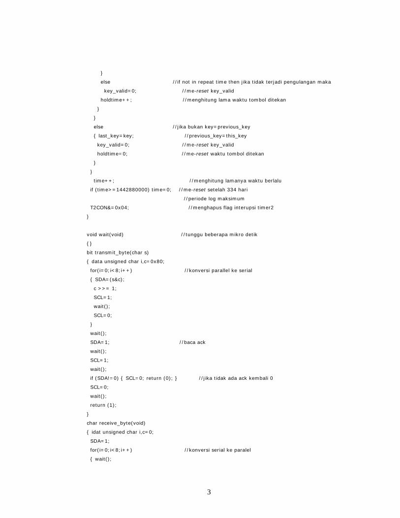
3
else //if not in repeat time then jika tidak terjadi pengulangan maka
key_valid=0; //me-reset key_valid
holdtime++; //menghitung lama waktu tombol ditekan
else //jika bukan key=previous_key
last_key=key; //previous_key=this_key
key_valid=0; //me-reset key_valid
holdtime=0; //me-reset waktu tombol ditekan
time++; //menghitung lamanya waktu berlalu
if (time>=1442880000) time=0; //me-reset setelah 334 hari
//periode log maksimum
T2CON&=0x04; //menghapus flag interupsi timer2
void wait(void) //tunggu beberapa mikro detik
bit transmit_byte(char s)
data unsigned char i,c=0x80;
for(i=0;i<8;i++) //konversi parallel ke serial
SDA=(s&c);
c >>= 1;
SCL=1;
wait();
SCL=0;
wait();
SDA=1; //baca ack
wait();
SCL=1;
wait();
if (SDA!=0) SCL=0; return (0); //jika tidak ada ack kembali 0
SCL=0;
wait();
return (1);
char receive_byte(void)
idat unsigned char i,c=0;
SDA=1;
for(i=0;i<8;i++) //konversi serial ke paralel
wait();
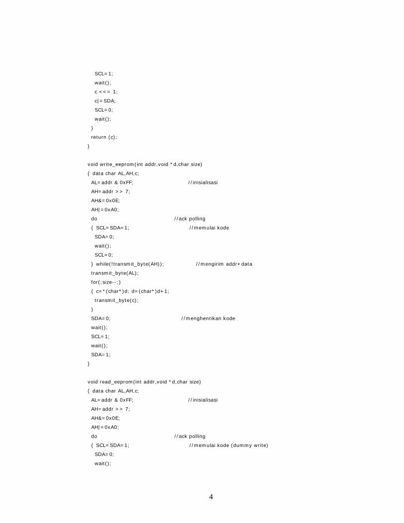
4
SCL=1;
wait();
c <<= 1;
c|=SDA;
SCL=0;
wait();
return (c);
void write_eeprom(int addr,void *d,char size)
data char AL,AH,c;
AL=addr & 0xFF; //inisialisasi
AH=addr >> 7;
AH&=0x0E;
AH|=0xA0;
do //ack polling
SCL=SDA=1; //memulai kode
SDA=0;
wait();
SCL=0;
while(!transmit_byte(AH)); //mengirim addr+data
transmit_byte(AL);
for(;size--;)
c=*(char*)d; d=(char*)d+1;
transmit_byte(c);
SDA=0; //menghentikan kode
wait();
SCL=1;
wait();
SDA=1;
void read_eeprom(int addr,void *d,char size)
data char AL,AH,c;
AL=addr & 0xFF; //inisialisasi
AH=addr >> 7;
AH&=0x0E;
AH|=0xA0;
do //ack polling
SCL=SDA=1; //memulai kode (dummy write)
SDA=0;
wait();
5
SCL=0;
while (!transmit_byte(AH)); //memulai pengiriman addr (dummy write)
transmit_byte(AL);
AH++; //inisialisasi (read)
SCL=1;
wait();
SDA=1; //memulai kode
wait();
SDA=0;
wait();
SCL=0;
wait();
transmit_byte(AH); //baca perintah
for(;size;size--)
c=receive_byte();
*(char*)d=c; d=(char*)d+1;
while(SDA!=1);
if((size-1)>0) SDA=0; //jika tidak ada byte teakhir yang dibaca kemudian kirim ack
else SDA=1; //yang lain tidak kirim ack
wait();
SCL=1;
wait();
SCL=0;
wait();
SDA=0; //menghentikan kode
wait();
SCL=1;
wait();
SDA=1;
void space(char n)
while(n--)
fprintf(LCD_out," ");
void calc_offset_gain(void)
idat char i=0,cal_mode;
idat signed long new_offset,h;
idat int cal_P1,cal_P2;
idat long cal_ADC1,cal_ADC2;
read_eeprom(Acal_mode,&cal_mode,sizeof(cal_mode));
if ((cal_mode==1) || (cal_mode==2)) //jika 1 atau 2 poin kalibrasi
6
read_eeprom(Acal_P1,&cal_P1,sizeof(cal_P1));
read_eeprom(Acal_P2,&cal_P2,sizeof(cal_P2));
read_eeprom(Acal_ADC1,&cal_ADC1,sizeof(cal_ADC1));
read_eeprom(Acal_ADC2,&cal_ADC2,sizeof(cal_ADC2));
if (cal_mode==1)
gain=default_gain; //penguatan sebanyak 1000 kali
else
gain=(1000*((long)cal_P1-(long)cal_P2))/((long)cal_ADC1-(long)cal_ADC2); //1000 kali
penguatan
new_offset=1000 * (long)cal_P1;
h=(long)gain * (long)cal_ADC1;
offset=new_offset-h; //1000 kali offset
else //jika bukan 1 atau 2 poin kalibrasi
write_eeprom(Acal_mode,&i,sizeof(i)); //gunakan nilai default
gain=default_gain; //penguatan 1000 kali
offset=default_offset; //1000 kali offset
void WRITE_LOGGER(void)
idat unsigned int average=sum/samples;
//tulis rata-rata ke EEPROM
write_eeprom(Alog_memory+(log_number*2),&average,sizeof(average));
log_sample=0; //reset sample flag me-reset flag sampling
if (++log_number==log_size) //batas memori tercapai
log_active=0; //mengatur logger untuk off
write_eeprom(Alog_nr,&log_number,sizeof(log_number));
//tulis nomor penyimpanan ke EEPROM
void goto_L1(void)
fputc(DP_HOME,LCD_set); //mulai ke baris 1 penampil
void goto_L2(void)
fputc(DP_LINE_2,LCD_set); //mulai ke baris 2 penampil
void ADCAverage(void)
sum*=(samples-1);
sum/=samples;
sum+=(unsigned int) fgetc(ADC); //dapat data tekanan udara terbaru
while (ADC_READY); //me-reset ADC_READY
if ((time%180000)==0) _ioinit(ADC); //mengkalibrasi ADC setiap jam
out=(((gain*sum)/samples)+offset+500)/1000;
7
// 500 sebagai offset untuk digit terakhir
void calc_trend(void)
idat unsigned int average;
if (!(time%1500)) //jika 30 detik berlalu kemudian hitung trend
average=sum/samples;
if (average>old_average) //jika actual_average > old_average
if (trend<2) trend++; //minimum 1 menit sebelum trend
else //trend harus diganti
if (trend>-2) trend--;
old_average=average; //old_average = actual_average
if (trend==2) trend_up=1; //mengatur trend yang baru
else if (trend==-2) trend_up=0;
void proces_command(char command)
idat char i,byte;
idat int nr;
idat unsigned int log_memory;
bit update_eeprom=0;
if (command==27) //jika tombol esc
ser_buf[0]='\0'; //hapus buffer
else //jika bukan tombol esc dan
if (command!=13) //jika bukan tombol enter
i=strlen(ser_buf); //tambah char ke buffer
if (i<7)
ser_buf[i++]=command;
ser_buf[i]='\0';
else //if enter key jika tombol enter
switch (ser_buf[0])
case 'l' : //jika "l max" maka kirim jumlah maksimum logger
if ((ser_buf[i=2]=='m') &&
(ser_buf[++i]=='a') &&
(ser_buf[++i]=='x'))
fprintf(SER_COMM,"%d",log_number);
//if "l nrxxx" then send logger value with number xxx
if ((ser_buf[i=2]=='n') &&
(ser_buf[++i]=='r'))
nr=ser_buf[++i]-48; nr*=100; //membangkitkan jumlah
8
byte=ser_buf[++i]-48; nr+=byte*10;
nr+=ser_buf[++i]-48;
fprintf(SER_COMM,"nr=%d ",nr);
read_eeprom(Alog_memory+(nr*2),&log_memory,sizeof(log_memory));
//mencari data
fprintf(SER_COMM,"%u",log_memory);
break;
ser_buf[0]='\0'; //menghapus buffer
long P_to_H(int p) //konversi tekanan udara ke ketinggian tempat
idat long h;
idat int dh,prc;
idat long factor;
idat char index;
factor=(long) p*10000; //P/Psea
factor/=(long) Psea;
factor-=2500; //tabel offset
index=factor/100;
dh=PH[index+1]-PH[index];
prc=factor%100;
h=(long) prc*dh;
h+=(long) PH[index]*100;
return (h);
void calc_time(long t,char *h,char *m, char *s)
//menghitung jam, menit, dan detik dari pencacah waktu
idat long x1;
x1=t%4320000;
*h=x1/180000;
x1=x1%180000;
*m=x1/3000;
*s=(x1%3000)/50;
void main(void)
idat unsigned char key=func_key;
idat char choice=1;
idat long height;
bit refresh_all=1;
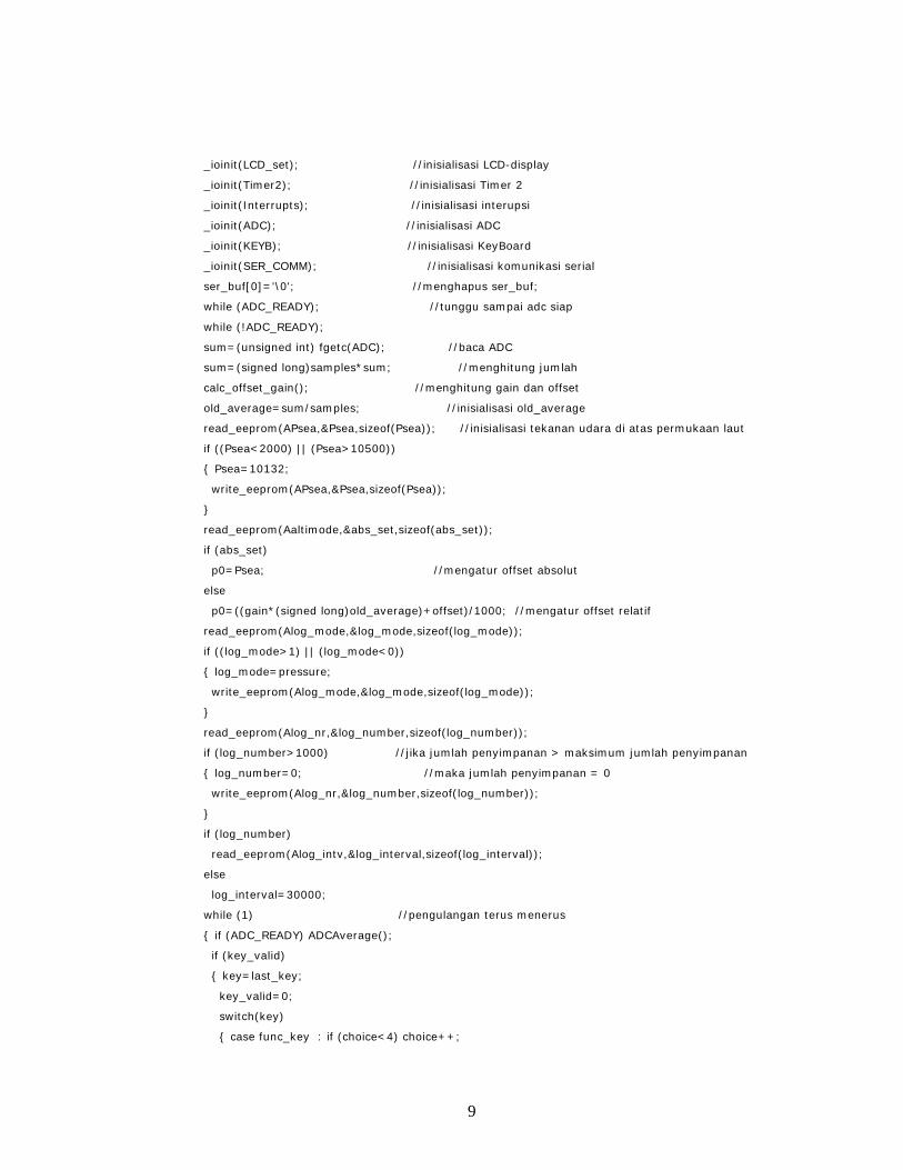
9
_ioinit(LCD_set); //inisialisasi LCD-display
_ioinit(Timer2); //inisialisasi Timer 2
_ioinit(Interrupts); //inisialisasi interupsi
_ioinit(ADC); //inisialisasi ADC
_ioinit(KEYB); //inisialisasi KeyBoard
_ioinit(SER_COMM); //inisialisasi komunikasi serial
ser_buf[0]='\0'; //menghapus ser_buf;
while (ADC_READY); //tunggu sampai adc siap
while (!ADC_READY);
sum=(unsigned int) fgetc(ADC); //baca ADC
sum=(signed long)samples*sum; //menghitung jumlah
calc_offset_gain(); //menghitung gain dan offset
old_average=sum/samples; //inisialisasi old_average
read_eeprom(APsea,&Psea,sizeof(Psea)); //inisialisasi tekanan udara di atas permukaan laut
if ((Psea<2000) || (Psea>10500))
Psea=10132;
write_eeprom(APsea,&Psea,sizeof(Psea));
read_eeprom(Aaltimode,&abs_set,sizeof(abs_set));
if (abs_set)
p0=Psea; //mengatur offset absolut
else
p0=((gain*(signed long)old_average)+offset)/1000; //mengatur offset relatif
read_eeprom(Alog_mode,&log_mode,sizeof(log_mode));
if ((log_mode>1) || (log_mode<0))
log_mode=pressure;
write_eeprom(Alog_mode,&log_mode,sizeof(log_mode));
read_eeprom(Alog_nr,&log_number,sizeof(log_number));
if (log_number>1000) //jika jumlah penyimpanan > maksimum jumlah penyimpanan
log_number=0; //maka jumlah penyimpanan = 0
write_eeprom(Alog_nr,&log_number,sizeof(log_number));
if (log_number)
read_eeprom(Alog_intv,&log_interval,sizeof(log_interval));
else
log_interval=30000;
while (1) //pengulangan terus menerus
if (ADC_READY) ADCAverage();
if (key_valid)
key=last_key;
key_valid=0;
switch(key)
case func_key : if (choice<4) choice++;
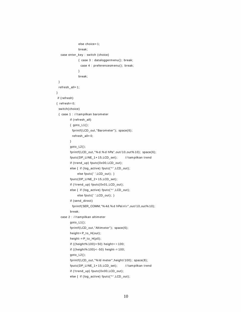
10
else choice=1;
break;
case enter_key : switch (choice)
case 3 : dataloggermenu(); break;
case 4 : preferencesmenu(); break;
break;
refresh_all=1;
if (refresh)
refresh=0;
switch(choice)
case 1 : //tampilkan barometer
if (refresh_all)
goto_L1();
fprintf(LCD_out,"Barometer"); space(6);
refresh_all=0;
goto_L2();
fprintf(LCD_out,"%d.%d hPa",out/10,out%10); space(6);
fputc(DP_LINE_1+15,LCD_set); //tampilkan trend
if (trend_up) fputc(0x00,LCD_out);
else if (log_active) fputc('*',LCD_out);
else fputc(' ',LCD_out);
fputc(DP_LINE_2+15,LCD_set);
if (!trend_up) fputc(0x01,LCD_out);
else if (log_active) fputc('*',LCD_out);
else fputc(' ',LCD_out);
if (send_direct)
fprintf(SER_COMM,"%4d.%d hPa\n\r",out/10,out%10);
break;
case 2 : //tampilkan altimeter
goto_L1();
fprintf(LCD_out,"Altimeter"); space(6);
height=P_to_H(out);
height-=P_to_H(p0);
if ((height%100)>50) height+=100;
if ((height%100)<-50) height-=100;
goto_L2();
fprintf(LCD_out,"%ld meter",height/100); space(8);
fputc(DP_LINE_1+15,LCD_set); //tampilkan trend
if (!trend_up) fputc(0x00,LCD_out);
else if (log_active) fputc('*',LCD_out);
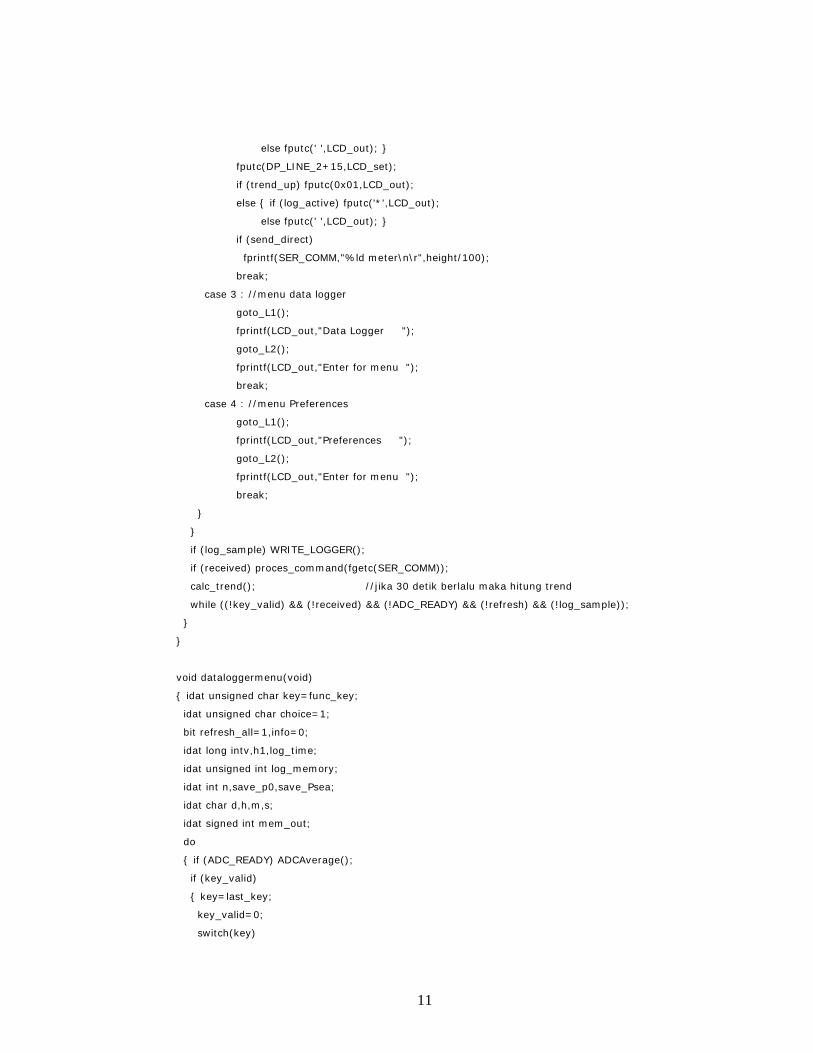
11
else fputc(' ',LCD_out);
fputc(DP_LINE_2+15,LCD_set);
if (trend_up) fputc(0x01,LCD_out);
else if (log_active) fputc('*',LCD_out);
else fputc(' ',LCD_out);
if (send_direct)
fprintf(SER_COMM,"%ld meter\n\r",height/100);
break;
case 3 : //menu data logger
goto_L1();
fprintf(LCD_out,"Data Logger ");
goto_L2();
fprintf(LCD_out,"Enter for menu ");
break;
case 4 : //menu Preferences
goto_L1();
fprintf(LCD_out,"Preferences ");
goto_L2();
fprintf(LCD_out,"Enter for menu ");
break;
if (log_sample) WRITE_LOGGER();
if (received) proces_command(fgetc(SER_COMM));
calc_trend(); //jika 30 detik berlalu maka hitung trend
while ((!key_valid) && (!received) && (!ADC_READY) && (!refresh) && (!log_sample));
void dataloggermenu(void)
idat unsigned char key=func_key;
idat unsigned char choice=1;
bit refresh_all=1,info=0;
idat long intv,h1,log_time;
idat unsigned int log_memory;
idat int n,save_p0,save_Psea;
idat char d,h,m,s;
idat signed int mem_out;
do
if (ADC_READY) ADCAverage();
if (key_valid)
key=last_key;
key_valid=0;
switch(key)
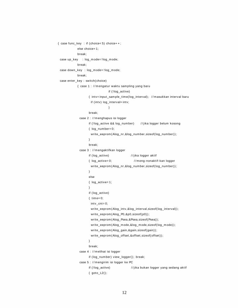
12
case func_key : if (choice<5) choice++;
else choice=1;
break;
case up_key : log_mode=!log_mode;
break;
case down_key : log_mode=!log_mode;
break;
case enter_key : switch(choice)
case 1 : //mengatur waktu sampling yang baru
if (!log_active)
intv=input_sample_time(log_interval); //masukkan interval baru
if (intv) log_interval=intv;
break;
case 2 : //menghapus isi logger
if (!log_active && log_number) //jika logger belum kosong
log_number=0;
write_eeprom(Alog_nr,&log_number,sizeof(log_number));
break;
case 3 : //mengaktifkan logger
if (log_active) //jika logger aktif
log_active=0; //meng-nonaktif-kan logger
write_eeprom(Alog_nr,&log_number,sizeof(log_number));
else
log_active=1;
if (log_active)
time=0;
intv_cnt=0;
write_eeprom(Alog_intv,&log_interval,sizeof(log_interval));
write_eeprom(Alog_P0,&p0,sizeof(p0));
write_eeprom(Alog_Psea,&Psea,sizeof(Psea));
write_eeprom(Alog_mode,&log_mode,sizeof(log_mode));
write_eeprom(Alog_gain,&gain,sizeof(gain));
write_eeprom(Alog_offset,&offset,sizeof(offset));
break;
case 4 : //melihat isi logger
if (log_number) view_logger(); break;
case 5 : //mengirim isi logger ke PC
if (!log_active) //jika bukan logger yang sedang aktif
goto_L2();
13
fprintf(LCD_out,"Sending to PC ");
read_eeprom(Alog_intv,&intv,sizeof(intv));
save_p0=p0; read_eeprom(Alog_P0,&p0,sizeof(p0));
save_Psea=Psea; read_eeprom(Alog_Psea,&Psea,sizeof(Psea));
log_time=0;
for(n=0;n<log_number;n++)
d=log_time/4320000; //hitung hari,
calc_time(log_time,&h,&m,&s); //jam, menit, detik
read_eeprom(Alog_memory+(n*2),&log_memory,sizeof(log_memory)); //cari data
h1=gain*(signed long)log_memory; h1=h1+offset+500; //hitung
tekanan udara
mem_out=h1/1000;
fprintf(SER_COMM,"day:%3d %02d:%02d:%02d ",d,h,m,s);
switch(log_mode)
case pressure : fprintf(SER_COMM,"%4d.%d
hPa\n\r",mem_out/10,mem_out%10); break;
case altitude : h1=P_to_H(mem_out);
h1-=P_to_H(p0);
if ((h1%100)>50) h1+=100;
if ((h1%100)<-50) h1-=100;
fprintf(SER_COMM,"%ld m\n\r",h1/100);
break;
log_time+=intv;
p0=save_p0;
Psea=save_Psea;
break;
break;
if (refresh)
refresh=0;
switch(choice)
case 1 : //menampilkan waktu sampling
goto_L1();
fprintf(LCD_out,"Sample Time ");
goto_L2();
if (!log_active) fprintf(LCD_out,"Enter to SET ");
else fprintf(LCD_out,"Logger active ");
break;
14
case 2 : //menghapus logger
goto_L1();
fprintf(LCD_out,"Clear datalogger");
goto_L2();
if (!log_active && log_number)
fprintf(LCD_out,"Enter to CLEAR ");
else
space(16);
break;
case 3 : //meng-nonaktif-kan logger
goto_L1();
switch(log_mode)
case pressure : fprintf(LCD_out,"Pres."); break;
case altitude : fprintf(LCD_out,"Alti."); break;
fprintf(LCD_out," logger ");
if (log_active) fprintf(LCD_out,"ON ");
else fprintf(LCD_out,"OFF");
goto_L2();
fprintf(LCD_out,"Enter to switch ");
break;
case 4 : //melihat isi logger
goto_L1();
switch(log_mode)
case pressure : fprintf(LCD_out,"Pressure"); break;
case altitude : fprintf(LCD_out,"Altitude"); break;
fprintf(LCD_out," logger ");
goto_L2();
if (log_number) fprintf(LCD_out,"Enter to view ");
else fprintf(LCD_out,"Logger empty ");
break;
case 5 : //mengirim isi logger ke PC
goto_L1();
switch(log_mode)
case pressure : fprintf(LCD_out,"Pressure"); break;
case altitude : fprintf(LCD_out,"Altitude"); break;
fprintf(LCD_out," logger ");
goto_L2();
if (!log_active)
if (log_number) fprintf(LCD_out,"Enter to send ");
else fprintf(LCD_out,"Logger empty ");
15
else fprintf(LCD_out,"Logger active ");
break;
if (log_sample) WRITE_LOGGER();
if (received) proces_command(fgetc(SER_COMM));
calc_trend(); //jika 30 menit berlalu maka hitung trend
while ((!key_valid) && (!received) && (!ADC_READY) && (!refresh) && (!log_sample));
while (key!=esc_key);
key_valid=0;
void view_logger(void)
idat unsigned char key=func_key;
idat int n=0,save_p0,save_Psea;
idat long log_time,log_intv;
idat unsigned int log_memory;
idat char d,h,m,s;
idat signed int mem_out;
bit refresh_all=1;
read_eeprom(Alog_intv,&log_intv,sizeof(log_intv));
save_p0=p0;
read_eeprom(Alog_P0,&p0,sizeof(p0));
save_Psea=Psea;
read_eeprom(Alog_Psea,&Psea,sizeof(Psea));
do
if (ADC_READY) ADCAverage();
if (key_valid)
key=last_key;
key_valid=0;
switch(key)
case up_key : if (n<(log_number-1)) n++; else n=0; break;
case down_key : if (n>0) n--; else n=(log_number-1); break;
refresh_all=1;
if (refresh)
refresh=0;
if (refresh_all)
refresh_all=0;
goto_L1();
log_time=log_intv*n; //menghitung waktu setiap sampling
d=log_time/4320000;
16
calc_time(log_time,&h,&m,&s);
fprintf(LCD_out,"day:%3d %02d:%02d:%02d",d,h,m,s);
goto_L2();
read_eeprom(Alog_memory+(n*2),&log_memory,sizeof(log_memory)); //waktu log
sekarang digunakan untuk variabel sementara, hanya untuk menyimpan RAM
//mem_out digunakan sebagai variabel sementara
read_eeprom(Alog_gain,&mem_out,sizeof(mem_out));
read_eeprom(Alog_offset,&log_time,sizeof(log_time));
log_time+=mem_out*(signed long)log_memory; log_time+=500;
//mulai sekarang mem_out berisi tekanan udara
mem_out=log_time/1000;
switch(log_mode)
case pressure : fprintf(LCD_out,"%4d.%d hPa",mem_out/10,mem_out%10); space(6);
break;
case altitude : log_time=P_to_H(mem_out);
log_time-=P_to_H(p0);
if ((log_time%100)>50) log_time+=100;
if ((log_time%100)<-50) log_time-=100;
fprintf(LCD_out,"%ld m",log_time/100); space(13);
break;
if (log_sample) WRITE_LOGGER();
if (received) proces_command(fgetc(SER_COMM));
calc_trend(); //jika 30 detik berlalu maka hitung trend
while ((!key_valid) && (!received) && (!ADC_READY) && (!refresh) && (!log_sample));
while (key!=esc_key);
key_valid=0;
p0=save_p0;
Psea=save_Psea;
long input_sample_time(long interval)
idat unsigned char key=func_key;
idat unsigned char digit=0;
bit cursor=0;
bit refresh_all=1;
idat char h,m,s;
do
if (ADC_READY) ADCAverage();
if (key_valid)
key=last_key;
key_valid=0;
switch(key)
17
case func_key : if (digit<6) digit++; else digit=0;
if (digit==1) digit=2;
if (digit==4) digit=5;
break;
case up_key : switch(digit)
case 0 : interval+=180000; break;
case 2 : interval+=30000; break;
case 3 : interval+=3000; break;
case 5 : interval+=500; break;
case 6 : interval+=50; break;
if (interval>1440000) interval=1440000;
break;
case down_key : switch(digit)
case 0 : interval-=180000; break;
case 2 : interval-=30000; break;
case 3 : interval-=3000; break;
case 5 : interval-=500; break;
case 6 : interval-=50; break;
if (interval<500) interval=500;
break;
case enter_key : fputc(DP_CURSOR_OFF,LCD_set); //switch cursor off
return (interval);
refresh_all=1;
if (refresh)
refresh=0;
cursor=!cursor;
if (cursor) fputc(DP_CURSOR_ON,LCD_set); //cursor on
else fputc(DP_CURSOR_OFF,LCD_set); //cursor off
if (refresh_all)
refresh_all=0;
goto_L1();
fprintf(LCD_out,"Interval"); space(8);
goto_L2();
calc_time(interval,&h,&m,&s);
fprintf(LCD_out,"%01d:%02d:%02d",h,m,s); space(9);
fputc(DP_LINE_2+digit,LCD_set);
if (log_sample) WRITE_LOGGER();
if (received) proces_command(fgetc(SER_COMM));
18
calc_trend(); //interval 30 detik untuk trend
while ((!key_valid) && (!received) && (!ADC_READY) && (!refresh) && (!log_sample));
while (key!=esc_key);
key_valid=0;
fputc(DP_CURSOR_OFF,LCD_set); //switch cursor off
return (0);
void preferencesmenu(void)
idat unsigned char key=func_key;
idat char choice=1;
idat signed int new_P,cal_P1,cal_P2;
idat signed long average;
idat unsigned char new_mode,cal_mode;
bit sea_pressure=(Psea==10132);
bit cal1_OK=0,cal2_OK=0;
#ifdef NORMAL
idat long hh;
idat signed int h_in,h,Pout,Poutfactor;
bit equal;
#endif
do
if (ADC_READY) ADCAverage();
if (key_valid)
key=last_key;
key_valid=0;
switch(key)
case func_key : if (choice<7) choice++; else choice=1;
break;
case enter_key : new_P=((gain*average)+offset)/1000;
read_eeprom(Acal_mode,&cal_mode,sizeof(cal_mode));
switch(choice)
case 1 : abs_set=set_alti_mode(abs_set);
if (abs_set) p0=Psea;
else p0=new_P;
break;
#ifdef NORMAL
case 2 : hh=P_to_H(out);
hh-=P_to_H(Psea);
h_in=(int)(hh/100); //mengkonversi dari cm ke m
h_in=input_new_value(h_in,0);
if(h_in>-2001)
Psea=10132;
19
equal=0;
Pout=7500;
Poutfactor=2425;
while(Poutfactor && !equal)
hh=P_to_H(Pout);
h=(int)(hh/100);
if(h_in>h)
Pout-=Poutfactor;
else
if(h_in<h)
Pout+=Poutfactor;
else
equal=1;
Poutfactor/=2;
//mulai sekarang hh digunakan sebagai Pn
hh=(long)Pout*10000;
hh/=(long)Psea;
if (hh<2600) hh=2600; //0,26 < Pn < 1,22
if (hh>12200) hh=12200;
Psea=(int)(((long)out*10000)/hh);
if (Psea<0) Psea=32767; //nilai maks untuk signed int
write_eeprom(APsea,&Psea,sizeof(Psea));
if (abs_set) p0=Psea;
sea_pressure=0;
break;
#endif
#ifdef VSL
case 2 : new_P=Psea;
new_P=input_new_value(new_P,1);
if (new_P)
Psea=new_P;
write_eeprom(APsea,&Psea,sizeof(Psea));
if (abs_set) p0=Psea;
sea_pressure=0;
break;
#endif
case 3 : if (!sea_pressure)
Psea=10132;
write_eeprom(APsea,&Psea,sizeof(Psea));
20
sea_pressure=1;
if (abs_set) p0=Psea;
break;
case 4 : send_direct=!send_direct; break;
case 5 : if (cal1_OK)
new_P=input_new_value(new_P,1);
if (new_P)
if (cal_mode==0) //tidak ada kalibrasi sebelumnya
new_mode=1;
write_eeprom(Acal_mode,&new_mode,sizeof(new_mode));
write_eeprom(Acal_P1,&new_P,sizeof(new_P));
average=sum/samples;
write_eeprom(Acal_ADC1,&average,sizeof(average));
calc_offset_gain();
break;
case 6 : if (cal2_OK)
new_P=input_new_value(new_P,1);
if (new_P)
if (cal_mode==1) //previous mode=1
new_mode=2;
write_eeprom(Acal_mode,&new_mode,sizeof(new_mode));
write_eeprom(Acal_P2,&new_P,sizeof(new_P));
average=sum/samples;
write_eeprom(Acal_ADC2,&average,sizeof(average));
calc_offset_gain();
break;
case 7 : new_mode=0; //default mode
write_eeprom(Acal_mode,&new_mode,sizeof(new_mode));
calc_offset_gain();
break;
break;
if (refresh)
refresh=0;
average=sum/samples;
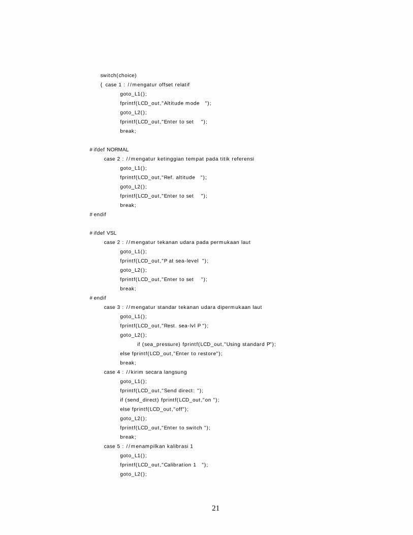
21
switch(choice)
case 1 : //mengatur offset relatif
goto_L1();
fprintf(LCD_out,"Altitude mode ");
goto_L2();
fprintf(LCD_out,"Enter to set ");
break;
#ifdef NORMAL
case 2 : //mengatur ketinggian tempat pada titik referensi
goto_L1();
fprintf(LCD_out,"Ref. altitude ");
goto_L2();
fprintf(LCD_out,"Enter to set ");
break;
#endif
#ifdef VSL
case 2 : //mengatur tekanan udara pada permukaan laut
goto_L1();
fprintf(LCD_out,"P at sea-level ");
goto_L2();
fprintf(LCD_out,"Enter to set ");
break;
#endif
case 3 : //mengatur standar tekanan udara dipermukaan laut
goto_L1();
fprintf(LCD_out,"Rest. sea-lvl P ");
goto_L2();
if (sea_pressure) fprintf(LCD_out,"Using standard P");
else fprintf(LCD_out,"Enter to restore");
break;
case 4 : //kirim secara langsung
goto_L1();
fprintf(LCD_out,"Send direct: ");
if (send_direct) fprintf(LCD_out,"on ");
else fprintf(LCD_out,"off");
goto_L2();
fprintf(LCD_out,"Enter to switch ");
break;
case 5 : //menampilkan kalibrasi 1
goto_L1();
fprintf(LCD_out,"Calibration 1 ");
goto_L2();
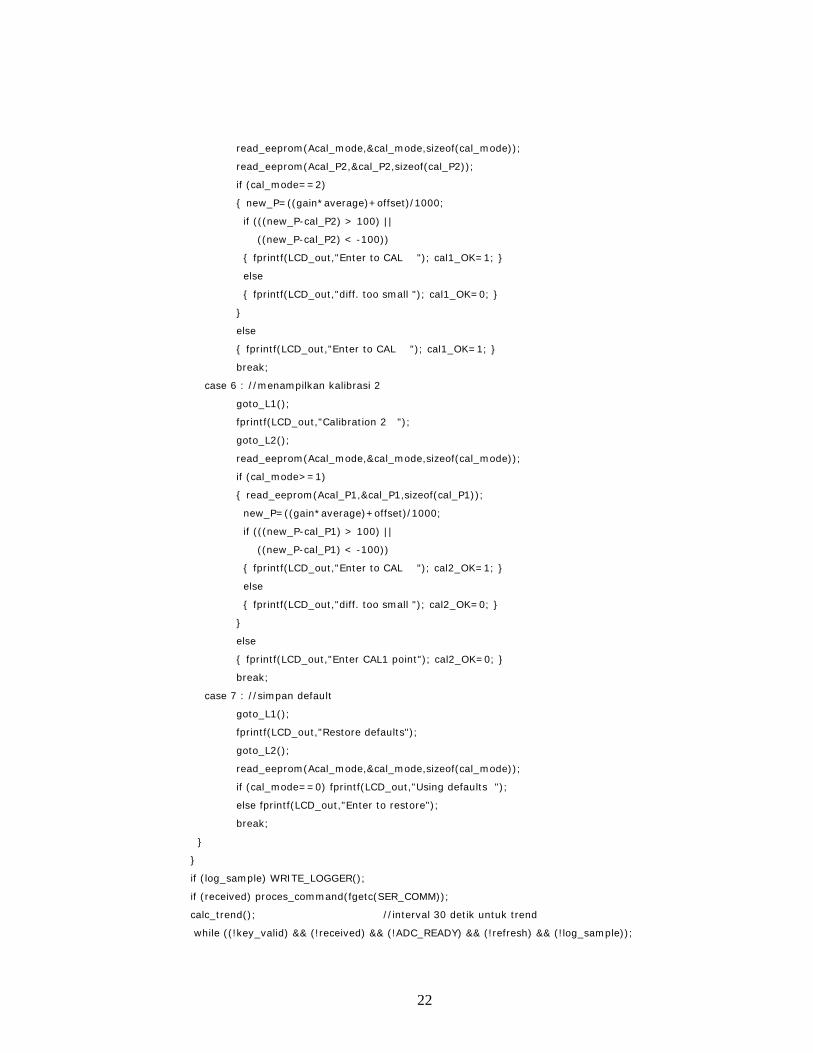
22
read_eeprom(Acal_mode,&cal_mode,sizeof(cal_mode));
read_eeprom(Acal_P2,&cal_P2,sizeof(cal_P2));
if (cal_mode==2)
new_P=((gain*average)+offset)/1000;
if (((new_P-cal_P2) > 100) ||
((new_P-cal_P2) < -100))
fprintf(LCD_out,"Enter to CAL "); cal1_OK=1;
else
fprintf(LCD_out,"diff. too small "); cal1_OK=0;
else
fprintf(LCD_out,"Enter to CAL "); cal1_OK=1;
break;
case 6 : //menampilkan kalibrasi 2
goto_L1();
fprintf(LCD_out,"Calibration 2 ");
goto_L2();
read_eeprom(Acal_mode,&cal_mode,sizeof(cal_mode));
if (cal_mode>=1)
read_eeprom(Acal_P1,&cal_P1,sizeof(cal_P1));
new_P=((gain*average)+offset)/1000;
if (((new_P-cal_P1) > 100) ||
((new_P-cal_P1) < -100))
fprintf(LCD_out,"Enter to CAL "); cal2_OK=1;
else
fprintf(LCD_out,"diff. too small "); cal2_OK=0;
else
fprintf(LCD_out,"Enter CAL1 point"); cal2_OK=0;
break;
case 7 : //simpan default
goto_L1();
fprintf(LCD_out,"Restore defaults");
goto_L2();
read_eeprom(Acal_mode,&cal_mode,sizeof(cal_mode));
if (cal_mode==0) fprintf(LCD_out,"Using defaults ");
else fprintf(LCD_out,"Enter to restore");
break;
if (log_sample) WRITE_LOGGER();
if (received) proces_command(fgetc(SER_COMM));
calc_trend(); //interval 30 detik untuk trend
while ((!key_valid) && (!received) && (!ADC_READY) && (!refresh) && (!log_sample));
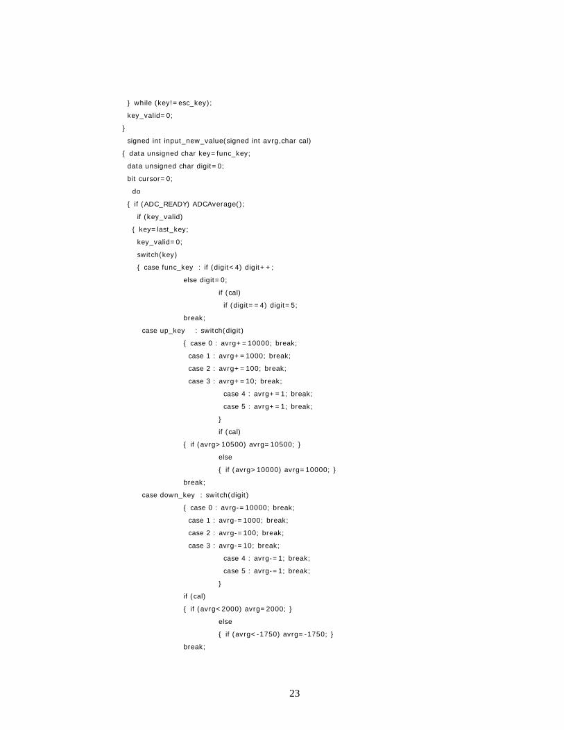
23
while (key!=esc_key);
key_valid=0;
signed int input_new_value(signed int avrg,char cal)
data unsigned char key=func_key;
data unsigned char digit=0;
bit cursor=0;
do
if (ADC_READY) ADCAverage();
if (key_valid)
key=last_key;
key_valid=0;
switch(key)
case func_key : if (digit<4) digit++;
else digit=0;
if (cal)
if (digit==4) digit=5;
break;
case up_key : switch(digit)
case 0 : avrg+=10000; break;
case 1 : avrg+=1000; break;
case 2 : avrg+=100; break;
case 3 : avrg+=10; break;
case 4 : avrg+=1; break;
case 5 : avrg+=1; break;
if (cal)
if (avrg>10500) avrg=10500;
else
if (avrg>10000) avrg=10000;
break;
case down_key : switch(digit)
case 0 : avrg-=10000; break;
case 1 : avrg-=1000; break;
case 2 : avrg-=100; break;
case 3 : avrg-=10; break;
case 4 : avrg-=1; break;
case 5 : avrg-=1; break;
if (cal)
if (avrg<2000) avrg=2000;
else
if (avrg<-1750) avrg=-1750;
break;
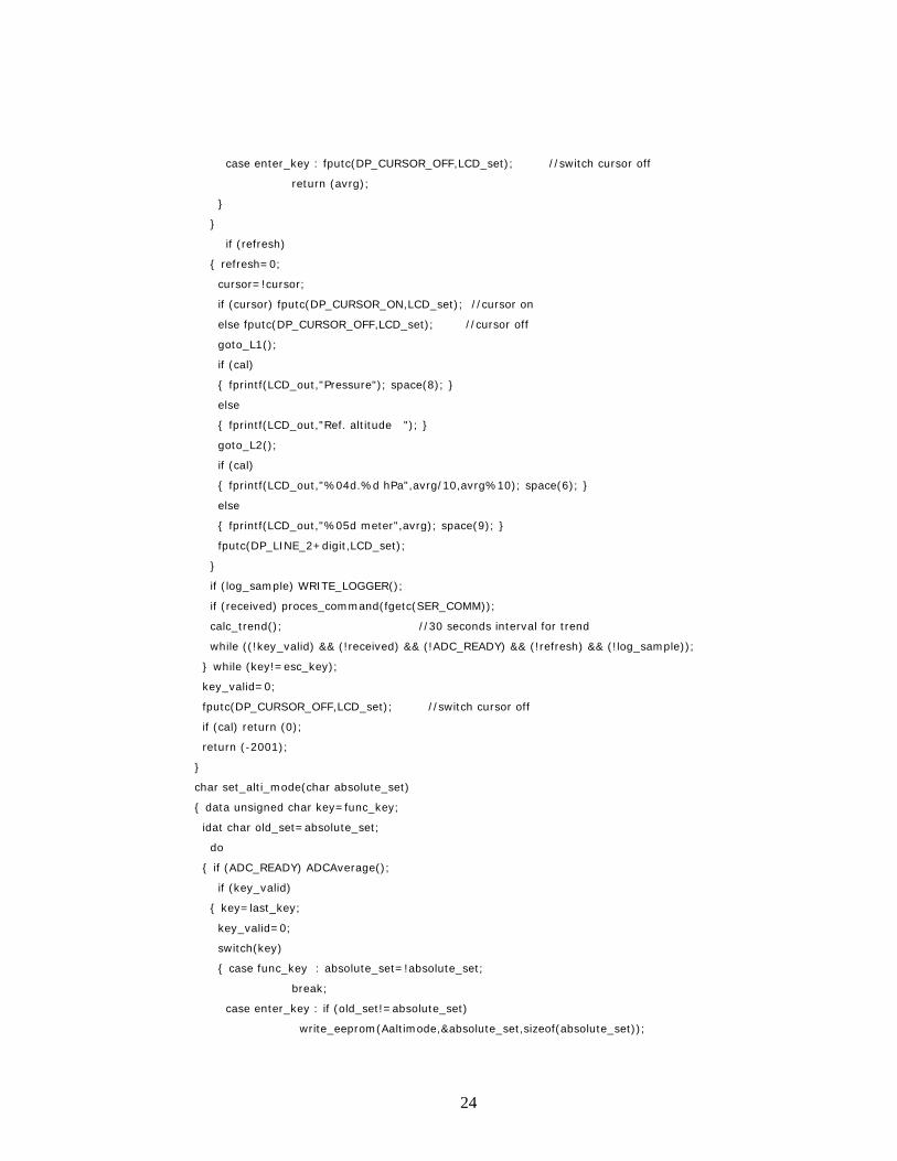
24
case enter_key : fputc(DP_CURSOR_OFF,LCD_set); //switch cursor off
return (avrg);
if (refresh)
refresh=0;
cursor=!cursor;
if (cursor) fputc(DP_CURSOR_ON,LCD_set); //cursor on
else fputc(DP_CURSOR_OFF,LCD_set); //cursor off
goto_L1();
if (cal)
fprintf(LCD_out,"Pressure"); space(8);
else
fprintf(LCD_out,"Ref. altitude ");
goto_L2();
if (cal)
fprintf(LCD_out,"%04d.%d hPa",avrg/10,avrg%10); space(6);
else
fprintf(LCD_out,"%05d meter",avrg); space(9);
fputc(DP_LINE_2+digit,LCD_set);
if (log_sample) WRITE_LOGGER();
if (received) proces_command(fgetc(SER_COMM));
calc_trend(); //30 seconds interval for trend
while ((!key_valid) && (!received) && (!ADC_READY) && (!refresh) && (!log_sample));
while (key!=esc_key);
key_valid=0;
fputc(DP_CURSOR_OFF,LCD_set); //switch cursor off
if (cal) return (0);
return (-2001);
char set_alti_mode(char absolute_set)
data unsigned char key=func_key;
idat char old_set=absolute_set;
do
if (ADC_READY) ADCAverage();
if (key_valid)
key=last_key;
key_valid=0;
switch(key)
case func_key : absolute_set=!absolute_set;
break;
case enter_key : if (old_set!=absolute_set)
write_eeprom(Aaltimode,&absolute_set,sizeof(absolute_set));
25
return (absolute_set);
if (refresh)
refresh=0;
goto_L1();
fprintf(LCD_out,"Altitude mode ");
goto_L2();
if (absolute_set) fprintf(LCD_out,"absolute");
else fprintf(LCD_out,"relative");
fprintf(LCD_out," alt. ");
if (log_sample) WRITE_LOGGER();
if (received) proces_command(fgetc(SER_COMM));
calc_trend(); //interval 30 detik untuk trend
while ((!key_valid) && (!received) && (!ADC_READY) && (!refresh) && (!log_sample));
while (key!=esc_key);
key_valid=0;
return (old_set);
1
#pragma romstring #define FORM_CONST #include <cc51.h> #include <stdio.h> #include "extio.h" rom char char1[]=0x04,0x0E,0x1F,0x04,0x04,0x04,0x04,0x00; //panah ke atas rom char char2[]=0x04,0x04,0x04,0x04,0x1F,0x0E,0x04,0x00; //panah ke bawah void load_chars(void) data char i; for(i=0;i<=7;i++) fputc(0x40+i,LCD_set); fputc(char1[i],LCD_out); fputc(0x48+i,LCD_set); fputc(char2[i],LCD_out); void _ioinit(FILE *f) //init LCD #define LCD P0 #define LCD_RS P2_0 #define LCD_RW P2_1 #define LCD_E P2_2 #define LCD_BUSY P0_7 #define DP_2_LINES 0x38 #define DP_ON 0x0d #define DP_CLEAR 0x01 #define DP_ENTRY 0x03 #define DP_INIT 0x30 #define CNTMAX 0x3a98 //15000 x 1us if (f==LCD_set) int data counter; char data i; for (i=0;i<3;i++) counter=CNTMAX; while (--counter>0); //tunggu selama 15 detik fputc(DP_INIT,LCD_set); //inisialisasi LCD sebanyak 3 kali fputc(DP_2_LINES,LCD_set); fputc(DP_ON,LCD_set); fputc(DP_CLEAR,LCD_set); fputc(DP_ENTRY,LCD_set); fputc(DP_CURSOR_OFF,LCD_set); load_chars(); // inisialisasi timer1 sebagai generator laju data dan inisialissi rs232 //9600 Baud, 1 startbit, 8 databits, 1 stopbit if (f==SER_COMM) //Timer 1 TMOD=0x20; //timer mode 2 TCON=0x40; //mulai timer TL1=0xFD; //inisialisasi nilai TH1=0xFD; //isi nilai secara otomatis //RS232 PCON=0x00; //SMOD=0 laju data single SCON=0x50; //serial mode 1, penerimaan diaktifkan TI=1; //inisialisasi nilai dari flag pengirim //inisialisasi Timer2 if (f==Timer2) //timer2 20ms TH2=0xB8; //inisialisasi nilai TL2=0x00;
2
RCAP2H=0xB8; //nilai timer HIGH byte RCAP2L=0x00; //nilai timer LOW byte T2MOD=0x00; //counter naik/turun diaktifkan T2CON=0x04; //mulai timer //inisialisasi Interupsi if (f==Interrupts) SPCR&=0x3F; //interupsi SPI diaktifkan IE=0x00; //mengaktifkan semua interupsi EA=1; //interupsi diperbolehkan ET2=1; //meng-enale-kan interupsi timer 2 TCON&=0x55; // menghapuskan semua flag interupsi TF2=EXF2=0; //menghapus flag interupsi timer 2 IP=0; //semua interupsi prioritas rendah PT2=1; //interupsi timer 2 prioritas tinggi //inisialisasi KeyBoard #define key P2 #define mask 0xf8 if (f==KEYB) key=mask; //mengatur port sebagai masukan //inisialisasi ADC #define ADC_CLK P1_1 #define ADC_DI P1_3 #define ADC_DO P1_2 #define ADC_DRDY P1_4 #define ADC_RESET P1_0 #define ADC_SET_WR 0x10 // mengatur register komunikasi untuk operasi tulis
ke register setup #define ADC_SETUP 0x66 //mengatur register setup #define ADC_SET_RD 0x38 // mengatur register komunikasi untuk operasi baca
ke register data /* ADC settings: ============= penguatan: 1x kalibrasi: self-calibration clk: 2.4576 MHz filter: 50Hz B/U: unipolair buffer: on FSYNC: off */ if (f==ADC) void _ADC_WRITE(char DO); int _ADC_READ(void); ADC_RESET=0; ADC_RESET=1; //untuk me-reset ADC ADC_DRDY=1; //diatur sebagai masukan _ADC_WRITE(ADC_SET_WR); _ADC_WRITE(ADC_SETUP); int _KEY_READ() key&=mask; return(key); void _ADC_WRITE(char DO) char i; for (i=0;i<=7;i++) ADC_CLK=0; ADC_DO=((DO & 0x80)!=0);
3
DO<<=1; ADC_CLK=1; int _ADC_READ(void) char i; int DI=0; ADC_DI=1; //diatur sebagai masukan _ADC_WRITE(ADC_SET_RD); for (i=0;i<=15;i++) ADC_CLK=0; DI<<=1; ADC_CLK=1; DI+=ADC_DI; return(DI); #define received RI #define char_in SBUF char _RS232_READ(void) if (received) received=0; //menghapus flag interupsi return(char_in); int _ioread(FILE *f) if (f==KEYB) return(_KEY_READ()); if (f==ADC) return(_ADC_READ()); if (f==SER_COMM) return(_RS232_READ()); int _iowrite(int c, FILE *f) #define char_out SBUF #define transmitted TI //jalur keluaran rs232 if (f==SER_COMM) while(!transmitted); transmitted=0; char_out=c; return(c); //jalur keluaran LCD if (f==LCD_out || f==LCD_set) LCD_RS=(f==LCD_out); //jika LCD_out kemudian instruksi data yang lain LCD_RW=0; LCD_E=0; LCD=c; //tulis data ke LCD LCD_E=1; LCD_E=0; LCD_BUSY=1; //mengatur LCD_BUSY sebagai masukan LCD_RS=0; LCD_RW=1; //mengatur RS dan RW ke operasi baca BUSY LCD_E=1; while(LCD_BUSY==1); //tunggu sampai LCD siap LCD_E=0; return(c);


![Barometer [2006]](https://img.pdfslide.tips/doc/110x75/577d35011a28ab3a6b8f584c/barometer-2006.jpg)