Embed Size (px)
Citation preview

An
A
nalys
A Thesis S
DepartNATION
sis and
Fe
Submitted
M
VLSI D
tment of ENAL INST
रा टरी
d App
eedth
in PartialAward
Master
Design &
Sauvagy(Roll N
ElectroniTITUTE
टरीय परौ योिODI
plicat
rough
l Fulfillmed of the De
of Tech
in
& Embeby
ya RanjaNo. 210E
ics & ComOF TEC
िगकी सISHA, IN
2012
tion o
h Log
ent of the Regree of
hnology
edded S
an SahooEC2304)
mmunicatHNOLOG
थान, राउरNDIA
of Im
gic
Requireme
y
Systems
o
tion EnginGY, ROU
रकला
mprov
ents for th
s
neering URKELA
ed
he

An
A
nalys
A Thesis S
DepartNATION
sis and
Fe
Submitted
M
VLSI D
Pro
tment of ENAL INST
रा टरी
d App
eedth
in PartialAward
Master
Design &
Sauvagy(Roll N
Under
of. Kama
ElectroniTITUTE
टरीय परौ योिODI
plicat
rough
l Fulfillmed of the De
of Techin
& Embeby
ya RanjaNo. 210E
r the Supeof
alakanta
ics & ComOF TEC
िगकी सISHA, IN
2012
tion o
h Log
ent of the Regree of
hnology
edded S
an SahooEC2304)
ervision
a Mahap
mmunicatHNOLOG
थान, राउरNDIA
of Im
gic
Requireme
y
Systems
o
atra
tion EnginGY, ROU
रकला
mprov
ents for th
s
neering URKELA
ed
he

CERTIFICATE
This is to certify that the thesis entitled “Analysis and Application of
Improved Feedthrough Logic” submitted by Mr. Sauvagya Ranjan Sahoo in partial
fulfillment of the requirements for the award of Master of Technology Degree in
Electronics and Communication Engineering with specialization in “VLSI Design and
Embedded Systems” during the session 2010-2012 at National Institute of Technology,
Rourkela is an authentic work carried out by him under my supervision and guidance.
To the best of my knowledge, the matter embodied in the thesis has not
been submitted to any other University/Institute for the award of any Degree or
Diploma.
Department of Electronics and Communication Engineering National Institute of Technology Rourkela-769008
Prof. Kamalakanta Mahapatra
Department of Electronics & Communication Engineering
National Institute of Technology, Rourkela
Date:
Place:

Acknowledgements
This project is by far the most significant accomplishment in my life and it would
have been impossible without the people who supported me and believed in me. I would like
to extend my gratitude and my sincere thanks to my honorable, esteemed supervisor Prof.
KamalaKanta Mahapatra, Department of Electronics & Communication Engineering. He
is not only a great professor with deep vision but also most importantly a kind person. I
sincerely thank for his exemplary guidance and encouragement. His trust and support
inspired me in the most important moments of making right decisions and I feel proud of
working under his supervision.
I am very much thankful to our Head of the Department, Prof. Sukadev Meher, for
providing us with best facilities in the department and his timely suggestions. I am very much
thankful to all my Professors Prof. D. P. Acharya, Prof. A. K. Swain, Prof. P. K. Tiwari,
and Prof. N. Islam for providing me their valuable suggestions during my thesis work and
for providing a solid background for my studies. They have been great sources of inspiration
to me and I thank them from the bottom of my heart.
I would like to show my gratitude to all my friends and especially to research scholars
Kanhu Charan Bbhuyan, Preetisudha meher, Vijay Sharma, Jagananth Mohanty,
Srinivas sharma, George Tom, Umakanta Nanda, Pallav Majhi, Venketesh and my
friends for all the thoughtful and mind stimulating discussions we had, which prompted us to
think beyond the obvious. I’ve enjoyed their companionship so much during my stay at NIT,
Rourkela. I would like to thank all those who made my stay in Rourkela an unforgettable and
rewarding experience.
I would like to thank my parents who taught me the value of hard work by their own
example. They rendered me enormous support being apart during the whole tenure of my stay
in NIT Rourkela. At last but above all, I owe this work to my much revered Lord for giving
me such a chance to work among these scholastic people and scholastic environment.
Sauvagya Ranjan sahoo

i
Abstract
Continuous technology scaling and increased frequency of operation of VLSI circuits
leads to increase in power density which raises thermal management problem. Therefore
design of low power VLSI circuit technique is a challenging task without sacrificing its
performance. This thesis presents the design of a low power dynamic circuit using a new
CMOS domino logic family called feedthrough (FTL) logic. Dynamic logic circuits are more
significant because of its faster speed and lesser transistor requirement as compared to static
CMOS logic circuits. The need for faster circuits compels designers to use FTL as compared
static and domino CMOS logic and the requirement of output inverter for cascading of
various logic blocks in domino logic are eliminated in the proposed design. The proposed
circuit for low power (LP-FTL) improves dynamic power consumption as compared to the
existing FTL and to further improve its speed we propose another circuit (HS-FTL). This
logic family improves speed at the cost of dynamic power consumption and area. Proposed
modified FTL circuit families provide better PDP as compared to the existing FTL.
Simulation results of both the proposed circuit using 0.18 µm, 1.8 V CMOS process
technology indicate that the LP-FTL structure reduces the dynamic power approximately by
35% and the HS-FTL structure achieves a speed up- 1.3 for 10-stage of inverters and 8-bit
ripple carry adder in comparison to existing FTL logic.
ii
Furthermore, we present various circuit design techniques to improve noise tolerance
of the proposed FTL logic families. Noise in deep submicron technology limits the reliability
and performance of ICs. The ANTE (average noise threshold energy) metric is used for the
analysis of noise tolerance of proposed FTL. A 2-input NAND and NOR gate is designed by
the proposed technique. Simulation results for a 2-input NAND gate at 0.18-µm, 1.8 V
CMOS process technology show that the proposed noise tolerant circuit achieves 1.79X
ANTE improvement along with the reduction in leakage power.
Continuous scaling of technology towards the nanometer range significantly increases
leakage current level and the effect of noise. This research can be further extended for
performance optimization in terms of power, speed, area and noise immunity.

iii
Contents
Abstract ................................................................................................................................ i
LIST OF FIGURES ............................................................................................................. vi
LIST OF TABLES ............................................................................................................. viii
CHAPTER 1
INTRODUCTION ........................................................................................................... 1
1.1 Introduction ................................................................................................................. 2
1.2 Literature Review ........................................................................................................ 3
1.2.1 Scaling ............................................................................................................. 3
1.2.2 Power .............................................................................................................. 4
1.2.2.1 Static power dissipation ............................................................................... 4
1.2.2.2 Dynamic power dissipation .......................................................................... 5
1.2.3 Propagation delay ............................................................................................ 6
1.2.4 Different Logic Styles ...................................................................................... 7
1.2.4.1 Static CMOS ................................................................................................ 7
1.2.4.2 Dynamic CMOS ........................................................................................... 9
1.2.4.3 Domino CMOS .......................................................................................... 12
1.2.4.4 Feedthrough Logic (FTL) ........................................................................... 13
1.3 Objective ................................................................................................................... 16
1.4 Thesis Organization ................................................................................................... 16

iv
CHAPTER 2
PROPOSED IMPROVED FTL .................................................................................... 17
2.1 Introduction ............................................................................................................... 18
2.2 LP-FTL Structure ...................................................................................................... 19
2.3 Performance analysis of LP-FTL ............................................................................... 20
2.3.1 Long chain of inverter .................................................................................... 21
2.3.2 8-bit Ripple Carry Adder................................................................................ 24
2.3.3 LFSR ............................................................................................................. 26
2.3.3.1 Operation of D-latch ................................................................................... 27
2.3.3.2 Simulation Results of LFSR ....................................................................... 28
2.4 HS-FTL Structure ...................................................................................................... 29
2.5 Performance analysis of HS-FTL ............................................................................... 30
CHAPTER 3
DESIGN OF 8-BIT RCA ............................................................................................... 32
3.1 Introduction ............................................................................................................... 33
3.2 8-bit RCA Design and Analysis ................................................................................. 35
3.2.1 Layout ........................................................................................................... 35
3.2.2 Creating I/O pins ............................................................................................ 37
3.2.3 DRC .............................................................................................................. 37
3.2.4 LVS ............................................................................................................... 37
3.2.5 Post Layout Simulation .................................................................................. 38
3.2.6 GDSII ............................................................................................................ 40

v
CHAPTER 4
NOISE ANALYSIS........................................................................................................ 41
4.1 Introduction ............................................................................................................... 42
4.2 Noise Sources ............................................................................................................ 43
4.2.1 Type of Noise ................................................................................................ 43
4.3 Logic Failure Due to Noise ........................................................................................ 44
4.4 Noise Tolerant Circuit Techniques ............................................................................. 45
4.4.1 Transistor stacking technique ......................................................................... 46
4.4.2 Triple Transistor technique ............................................................................ 47
4.5 Simulation Results and comparison............................................................................ 48
4.5.1 Noise Immunity Curve ................................................................................... 48
4.5.2 Noise injection Circuit ................................................................................... 48
4.5.3 ANTE ............................................................................................................ 49
4.5.4 Noise tolerance analysis for Inverter .............................................................. 50
4.5.5 Noise tolerance analysis for NAND2 ............................................................. 51
4.5.6 Noise tolerance analysis for NOR2 ................................................................ 52
CHAPTER 5
CONCLUSIONS & FUTURE RESEARCH ................................................................ 53
5.1 Conclusions ............................................................................................................... 54
5.2 Future Research ......................................................................................................... 54
REFERENCES ................................................................................................................... 55

vi
LIST OF FIGURES
Figure1.1Switching and short-circuit current elements in static CMOS ................................. 5
Figure1. 2 (a) CMOS logic gates as a combination of PUN and PDN (b) CMOS inverter ...... 7
Figure1. 3 Basic Structure of a Dynamic CMOS ................................................................... 9
Figure1. 4 (a) cascade of dynamic CMOS inverter .............................................................. 11
Figure1. 5 Domino CMOS Logic ........................................................................................ 12
Figure1. 6 (a) Basic structure of FTL [15]. (b) Inverter using FTL. ...................................... 14
Figure1.7 (a) Long chain of inverters using FTL (10-Stages) (b) plot of output voltages from
1st stage (N1) to 10
th stage (N10). ........................................................................................ 14
Figure 2.1 (a) Proposed modified low power FTL structure (LP-FTL) (b) LP-FTL inverter. 19
Figure 2.2 Variation in power, delay and area w.r.t. number of stacked PMOS .................... 20
Figure 2.3 Long Chain of LP-FTL inverter .......................................................................... 21
Figure 2.4 Plot of the output voltages from 1st stage (N1) to 10
th stage (N10) of inverters. (a)
For FTL (b) For LP-FTL ..................................................................................................... 21
Figure 2.5 (a) Layout of FTL inverter (10-stage) (b) av_extracted view ............................... 22
Figure 2. 6 (a) Layout of LP-FTL inverter (10-stage) (b) av_extracted view ........................ 22
Figure 2. 7 Ripple Carry Adder for LP-FTL structure (a) carry cell (b) sum cell .................. 24
Figure 2. 8 Effect of load capacitance on propagation delay ................................................ 25
Figure 2. 9 LFSR using LP-FTL flip-flop ............................................................................ 26
Figure 2. 10 Positive edge triggered D flip-flop ................................................................... 26
Figure 2. 11 D-latch using LP-FTL ..................................................................................... 27
Figure 2. 12 Output wave form at the X1, X2, X3, X4 of LFSR and total power ................. 28
Figure 2. 13 (a) Proposed modified HS-FTL. (b) HS-FTL inverter ..................................... 29
Figure 2. 14 Plot of the output voltages from 1st stage (N1) to 10th stage (N10) of inverter in
HS-FTL .............................................................................................................................. 30
Figure 3.1 Analog IC design Flow ....................................................................................... 34
Figure 3.2 Layout of LP-FTL Full Adder ............................................................................ 35
Figure 3.3 Layout of 8-bit Ripple Carry Adder .................................................................... 36
Figure 3.4 DRC run window ............................................................................................... 37
Figure 3.5 LVS run window ................................................................................................ 37
Figure 3.6 av_extracted view of 8-bit Ripple Carry Adder ................................................... 38
Figure 3.7 configure window of 8-bit RCA for av_extracted view ....................................... 39
Figure 3.8 GDS II window .................................................................................................. 40

vii
Figure 4.1 Noise at the Input of LP-FTL Inverter ................................................................ 44
Figure 4.2(a) Stacked Transistor inverter (b) Stacked Transistor NAND2 ............................ 46
Figure 4. 3(a) Triple transistor NAND2 (b) Triple transistor NOR2 ..................................... 47
Figure 4.4 (a)Noise immunity curve [22] (b) NIC [17] ........................................................ 48
Figure 4.5 Noise immunity curves for inverter .................................................................... 50
Figure 4.6 Noise immunity curves for NAND2 ................................................................... 51
Figure 4. 7Noise immunity curves for NOR2 ...................................................................... 52
viii
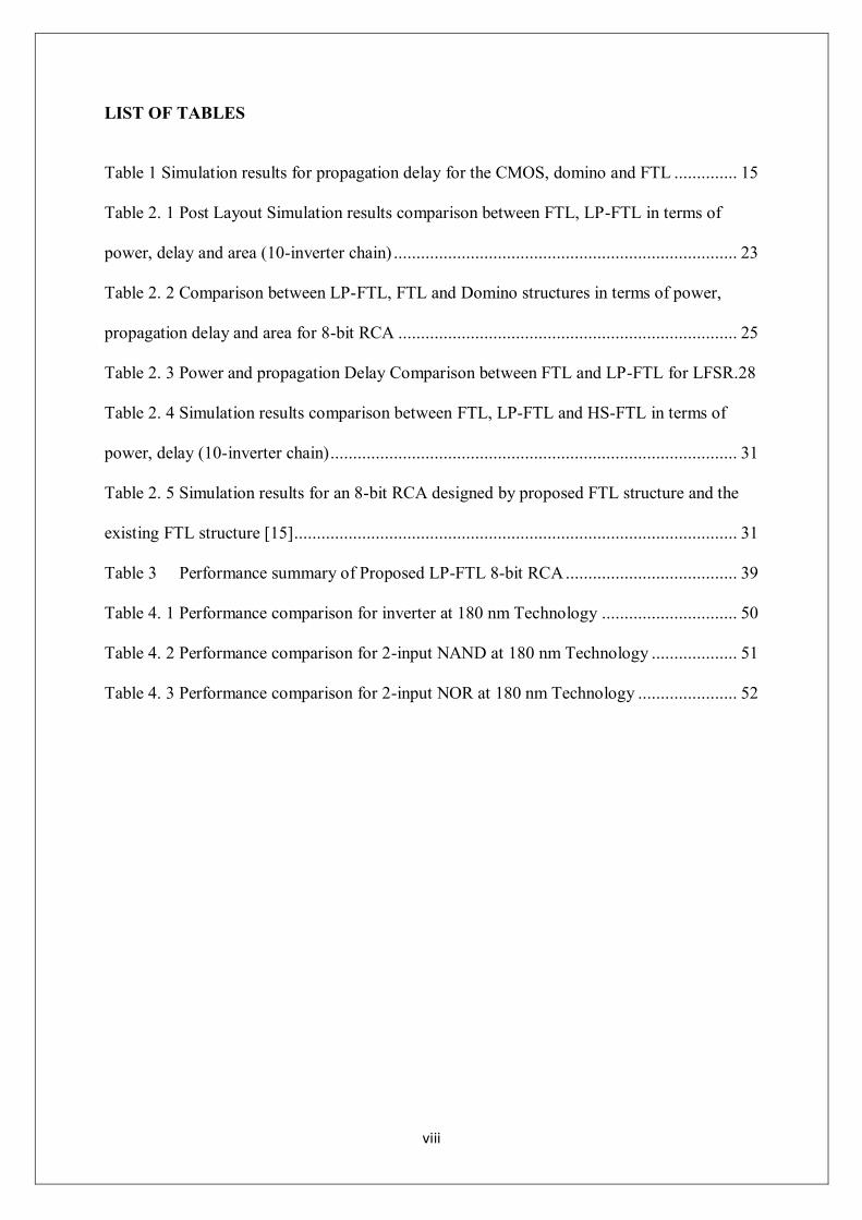
LIST OF TABLES
Table 1 Simulation results for propagation delay for the CMOS, domino and FTL .............. 15
Table 2. 1 Post Layout Simulation results comparison between FTL, LP-FTL in terms of
power, delay and area (10-inverter chain) ............................................................................ 23
Table 2. 2 Comparison between LP-FTL, FTL and Domino structures in terms of power,
propagation delay and area for 8-bit RCA ........................................................................... 25
Table 2. 3 Power and propagation Delay Comparison between FTL and LP-FTL for LFSR.28
Table 2. 4 Simulation results comparison between FTL, LP-FTL and HS-FTL in terms of
power, delay (10-inverter chain) .......................................................................................... 31
Table 2. 5 Simulation results for an 8-bit RCA designed by proposed FTL structure and the
existing FTL structure [15] .................................................................................................. 31
Table 3 Performance summary of Proposed LP-FTL 8-bit RCA ...................................... 39
Table 4. 1 Performance comparison for inverter at 180 nm Technology .............................. 50
Table 4. 2 Performance comparison for 2-input NAND at 180 nm Technology ................... 51
Table 4. 3 Performance comparison for 2-input NOR at 180 nm Technology ...................... 52

Page 1
CHAPTER 1
INTRODUCTION
.

Chapter 1 Introduction
Page 2
1.1 Introduction
The invention of transistor brought about a giant technology leap in microelectronics.
With the advent of transistor and the arrival of IC’s, power dissipation is a lesser concern.
Greater emphasis is placed on performance and size. To continue to improve the performance
of circuits and to integrate more functions into chip, feature size reduces significantly. As a
result, the magnitude of power per unit area (power density) has kept growing and the
problem of heat removal and cooling getting worse. In the last few years we have seen that
the emerging battery powered portable applications like pocket calculator, hearing aids,
implantable pacemakers should consume less power for longer life. Consequently, ever since
then power reduction has become one of the most critical factors in the evolution of
technology. Even with the scaling of supply voltages power dissipation has not reduced
significantly because more number of functionality is embedded in a single chip. An
alternative to solve this problem could mean accepting either the large cost for cooling
subsystem. Ineffective cooling degrades reliability. As a result today it is widely accepted
that power efficiency is another important design criteria along with area and performance.
So the power consumption should be minimized at each abstraction level and at each phase of
the design process.

Chapter 1 Introduction
Page 3
1.2 Literature Review
Reducing the power consumption of CMOS integrated circuits along with improving
its performance has been a topic of great interest in recent years. The various design
techniques proposed in the last two decades trade power for performance. This is achieved
through a mix of dynamic and static circuit styles [1], use of dual threshold voltage transistors
[2] and dual supply voltages [3]. For many applications, speed improvement is achieved at
the expense of power. The dynamic design in [3] uses high supply voltage for logic
evaluation and low supply voltage for clocking dynamic logic. The adder designed in [4] uses
architectural technique to reduce the short circuit current; the research work in [5] uses two
dynamic gates between three static gates. Looking at the aspects of scaling, power dissipation
an exhaustive literature survey has made
1.2.1 Scaling
CMOS technology is the dominant one in today’s IC because of its high speed, low
power and high packaging density. With continuous technology scaling i.e. reduction in
feature size leads to high packaging density but it leads to increase in current density as well
as power density. The large increase in current or power density causes serious reliability
problems for the scaled transistors like oxide breakdown, hot carrier injection [6, 7, 8, 9].
This increase in power density can be reduced by supply voltage (VDD) scaling because of the
quadratic relationship between power and VDD, but the rate of supply voltage scaling is not as
fast as rate at which device dimensions are scaled because of various physical limitations like
built in junction potential or silicon band gap which can’t be scaled further.
Continuous scaling of CMOS technology makes noise becomes an equal important
metrics like power, performance and area. To maintain performance with the scaling of
supply voltage threshold voltage is also scaled down, resulting in reduction of noise margin.
In current CMOS technology with reduced spacing between interconnect and higher

Chapter 1 Introduction
Page 4
operating frequency makes capacitive and inductive coupling [10] to increase significantly
resulting in severe side effects on signal integrity.
1.2.2 Power
Ideally, in CMOS circuits the output node is either connected to VDD or GND. Due to
absence of direct path between VDD and GND CMOS circuits dissipates zero static power.
But practically MOS transistor never acts as perfect switch. There is always leakage current
which leads to static power dissipation. The various sources of power dissipation [11, 12] in
CMOS are,
Static Power Dissipation
Dynamic power Dissipation
The total power in a static CMOS is given by [11]
)1.1(CircuitShortSwitchingStaticTotal PPPP
1.2.2.1 Static power dissipation (PStatic)
It is the power dissipated when there is no switching activity within the circuit.
Ideally, CMOS circuit dissipates no static power, since there is no direct path from VDD to
GND. But practically MOS transistor never acts as perfect switch. There is always leakage
current which flows when the input(s) to and the outputs of a gate are not changing, leads to
static power dissipation. But as the supply voltage is being scaled down to reduce dynamic
power, low VTH transistors are used to maintain performance. Reduction in VTH of transistor
leads to greater leakage current [11].
The static power dissipation is given by
P Static = VDD * I leakage (1.2)

Chapter 1 Introduction
Page 5
Figure1.1Switching and short-circuit current elements in static CMOS
1.2.2.2 Dynamic power dissipation
It is the dominant portion of power dissipation which occurs due to transition at gate
outputs. It consist two components of power dissipation
(i) Switching Power dissipation (Pswitching)
As the nodes in a digital CMOS circuit transition back and forth between the two
logic levels, the capacitance associated with the nodes gets charged and discharged. The
power dissipated during this process is called as switching power and it is the major source of
power dissipation in CMOS circuits.
For a static CMOS circuit with N switching nodes operating at clock frequency f clk,
the switching power is given by [13]
)3.1(1
clkswingDDi
N
iSwitching fVVCP
Where αi is the switching activity at node i
VDD is the supply voltage
Vswing Voltage swing at node i
αi Ci is the effective switch capacitance per cycle at node i
VDD
PUN
In 1
Node i
PDN
In 1
In N
In N
In 2
In 2
Ci
Charging
current
discharging
current
ISC

Chapter 1 Introduction
Page 6
(ii) Short Circuit Power Dissipation (Pshort-circuit)
This is due to short circuit current (ISC) which flows directly from VDD to GND when
both PMOS and NMOS transistor are on. When the input to the gate stable at either logic
level only PMOS or NMOS transistors are ON. Hence no short circuit current flows. But
when output of a gate switches in response to change in inputs, both PMOS and NMOS
transistors are conducts simultaneously for a short interval of time. This interval of time
depends upon rise or fall time of input signal and causes short circuit power dissipation.
PShort-circuit = VDD * ISC (1.4)
1.2.3 Propagation delay
The dependency of propagation delay on circuit parameter is given by [14]
)5.1()(
THDD
DDLd
VVk
VCT
Where α is the velocity saturation index varies between 1and 2
K depends upon W/L
From equation 1.3 and 1.5, the power dissipation and propagation delay both depends
upon the supply voltage (VDD). The scaling of supply voltage causes the reduction in power
whereas the propagation delay significantly increases. So for each design depending upon its
application there exist a tradeoff between power and delay. Hence various logic styles are
used to construct logic gates depending upon its application in terms of power, speed and
area.

Chapter 1 Introduction
Page 7
1.2.4 Different Logic Styles
1.2.4.1 Static CMOS
Static CMOS circuits consists a pull up network (PUN) and a pull down network
(PDN) as in Figure 1.2 (a). The PUN block consist PMOS transistors which pull up the
output node (OUT) to VDD and the PDN block consists NMOS transistors which pull down
the OUT node to GND. At any instant of time either the pull up or pull down block is on so
that the node OUT is always at VDD or GND. The size of PMOS devices is made larger than
the NMOS devices because the mobility of PMOS is lower than the NMOS. The structure of
a CMOS inverter is shown in Figure 1.2 (b). It consist a PMOS and NMOS transistor in
series. The operation of the circuit is as follows; when A is HIGH (VDD) TN is ON and TP is
OFF. A direct path exists from node Y to ground, resulting in a steady state value of 0V.
When A is LOW (0 V) TP is ON and TN is OFF, resulting in a steady voltage of VDD at node
Y.
Figure1. 2 (a) CMOS logic gates as a combination of PUN and PDN (b) CMOS inverter
VDD
PUN
In 1
OUT (In 1, In 2 … In N)
PDN
In 1
In N
In N
In 2
In 2
TN
A
TP
VDD
CL
Y= A’
(a) (b)

Chapter 1 Introduction
Page 8
Advantages
1. Since the voltage swing at node OUT is equal to the supply voltage i.e. VDD or GND.
This results in high noise margin
2. The output is independent of device sizes results in non-ratio logic.
3. High input impedance leads to high fan-out.
4. Low output impedance leads to less sensitive to noise and disturbance.
5. The absence of direct path between VDD and GND leads to zero static power
consumption.
6. Switching threshold is equals to VDD/2 leads to more robust.
Limitation
1. When the input makes transition from HIGH to LOW or vice versa both PMOS and
NMOS transistors are ON for a short interval of time leads to short circuit current.
2. A fan-in of N requires 2N devices results in larger device area.

Chapter 1 Introduction
Page 9
1.2.4.2 Dynamic CMOS
The basic structure of a dynamic logic gate is shown in Figure 1.3. The PDN network
consist only NMOS transistors as in static CMOS. It requires an additional clock input (CLK)
and uses a sequence of precharge and evaluation phase.
Figure1. 3 Basic Structure of a Dynamic CMOS
Precharge phase:
When CLK=0, the node OUT is precharged to VDD through TP .the PDN is disabled because
TE is OFF.
Evaluation phase:
When CLK=1, TP is OFF and TE is ON. The node OUT conditionally discharges based upon
input value to the PDN. During evaluation phase, the only possible path from node OUT to
supply rail is GND. The node OUT can only discharge in evaluation phase and charges to
VDD during precharge phase.
TE
CLK TP
CL
VDD
In 1
OUT (In 1
, In 2
… In N
)
PDN I
n N
In 2
CLK

Chapter 1 Introduction
Page 10
Advantages
1. Number of transistor reduces from 2N as in static CMOS to N+2, hence reduction in
device area.
2. Logic function is implemented only by the NMOS transistors, hence faster.
3. Non-ratio logic.
4. Switching point is threshold voltage of NMOS transistors in the evaluation phase.
5. Only consumes dynamic power.
Limitations
1. Low noise margin due to reduction in switching threshold.
2. Output is in high impedance state if PDN is turned off during evaluation phase.
3. It suffers from charge leakage, charge sharing.
The major limitation of dynamic CMOS circuit is the cascading of dynamic gates,
illustrated by two cascaded inverter as shown in Figure1.4 (a). During precharge phase the
output of both the inverters i.e. OUT1 and OUT2 precharged to VDD. When the IN makes 0
to1 transition as shown in Figure 1.4 (b), OUT1 starts to discharge on the rising edge of CLK.
The node OUT2 should remain at VDD as IN=1, but due to finite propagation delay for the
input to discharge node OUT1 to GND, node OUT2 also starts discharging as long as OUT1 is
above switching threshold (VTN) of TN2. So there exists a conducting path from node OUT2 to
GND, results in loss of previously stored charge. This conducting path from OUT2 to GND is
disabled when voltage at node OUT1 reaches VTN, makes TN2 turns off and leaves node OUT2
at an incorrect voltage level which cannot be recovered.

Chapter 1 Introduction
Page 11
Figure1. 4 (a) cascade of dynamic CMOS inverter
This cascading problem can be overcome by setting the voltage at the input to next
stage at logic 0 during precharge phase. By doing this all transistors in the PDN are turned off
after precharge and no inadvertent discharging of stored charge takes place. This can be
achieved by using Domino Logic.
TE
CLK
TP
VDD
IN
TE
TP
VDD
CLK
CLK
OUT1
OUT1
OUT2
OUT2
CLK
IN
t
VTn
ΔV
CLK
TN1
TN2
(a) (b)

Chapter 1 Introduction
Page 12
1.2.4.3 Domino CMOS
The domino logic structure is similar to that of dynamic logic along with a static
CMOS inverter is used to avoid cascading problem as shown in Figure 1.5. During precharge
phase (CLK=0), the output of dynamic logic is charges to VDD and the output of inverter is
become zero. During evaluation phase (CLK=1), the node OUT makes only transition from 0
to 1. Since in the precharge phase the node OUT discharges to logic 0, hence the false
evaluation is avoided during cascading of various domino blocks.
As it uses static inverter only non-inverting logic can be realized and it increases
propagation delay.
Figure1. 5 Domino CMOS Logic
The above 3- discussed logic styles provide low power consumption but these
structures suffer from reduction in speed. To overcome this limitation a new logic style called
as feedthrough logic (FTL) in [15] is used.
TE
CLK T
P
CL
VDD
In 1
OUT (In 1
, In 2
… In N
)
PDN I
n N
In 2
CLK
Chapter 1 Introduction
Page 13
1.2.4.4 Feedthrough Logic (FTL)
To improve the performance of CMOS logic circuits in terms of speed and power
further a new logic family called feedthrough logic (FTL) was proposed in [15]. The FTL
concept was successfully used for the design of low power and high performance arithmetic
circuits [16]. This logic works on domino concept along with the important feature that gates
begin evaluation even before all their inputs are valid. This leads to faster evaluation in
computational blocks. The problems associated with domino logic [6] such as charge sharing,
need for output inverters are completely eliminated by FTL, thus reduces chip area, delay and
performance.
FTL logic in [15] shows high design flexibility; it can be used in domino like
cascaded stages, differential style and pipelined with fast dynamic latch. FTL was
successfully employed by the authors for integrated circuits in GaAs technology in [16].
It is also a type of dynamic logic. The basic structure of FTL is shown in Figure 1.6
(a). It consist a NMOS reset transistor TR for resetting the output node (OUT) to low logic
level, a pull up PMOS load transistor TP and a PDN. TP and TR controlled by the clock signal
CLK.
The basic operating principle of FTL was presented in [15] and is briefed here. When
CLK goes HIGH, (reset phase) TR is turned on and the output node (OUT) pulled to ground
through TR. During evaluation phase i.e. when CLK goes LOW, TR is turned off, and the
voltage at node OUT rises initially then it becomes logic HIGH (i.e. VOH = VDD) or LOW
(VOL) depending upon inputs to the PDN block. If the PDN block evaluates to HIGH then
node OUT pulled up towards VDD otherwise it will pulled down to VOL. So when CLK goes
from HIGH to LOW, node OUT makes partial transition from VTH to either VOH or VOL
depending upon inputs to PDN.

Chapter 1 Introduction
Page 14
Figure1. 6 (a) Basic structure of FTL [15]. (b) Inverter using FT
Figure1.7 (a) Long chain of inverters using FTL (10-Stages) (b) plot of output
voltages from 1st stage (N1) to 10
th stage (N10)
A long chain of inverter designed by using FTL is shown in Figure 1.7 (a). When CLK
goes HIGH the voltage at all the output nodes i.e. N1, N2 ….N10 pulled to ground through TR
at each stage as shown in Figure 1.7 (b). During evaluation phase i.e. when CLK goes LOW,
TR is turned off, and the voltage at output node (N1, N2….N10) initially rises to VTH then it
conditionally evaluates to either logic HIGH (VOH) or LOW (VOL) depending upon input to
the TN at each stage. Since the transition at output node occurs only from VTH to either VOH or
VOL as shown in Figure 1.7 (b). As a result both low-to-high and high-to-low propagation
delay reduces.
TR
TP
A
TR
CLK
TP
VDD
In 1
OUT (In 1
, In 2
… In N
)
PDN I
n N
In 2
CLK CLK
TN
CLK
Y= A’
VDD
(a) (b)
Time
VTH
Ou
t
N1
N2
N10
N9 CLK
VOL
TP
TN
V
IN
N1
V
CLK
CL C
L
N2
TR
TP
TN T
R
VOH
(a) (b)
Chapter 1 Introduction
Page 15
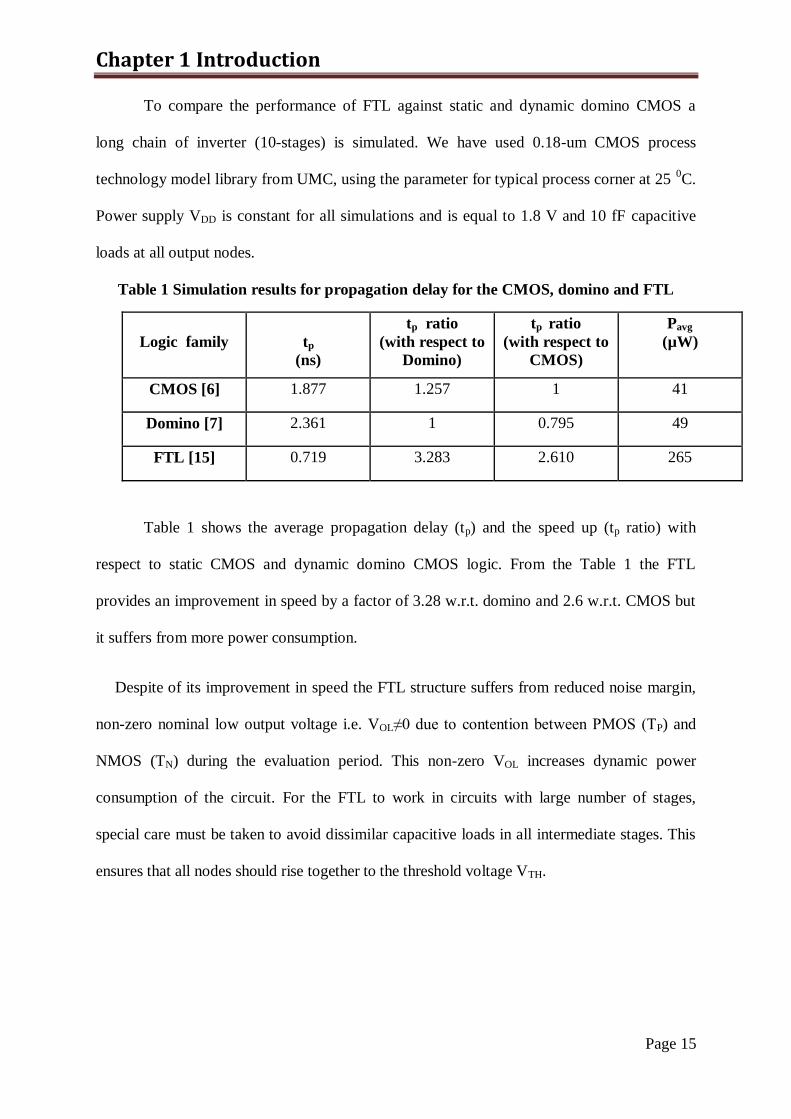
To compare the performance of FTL against static and dynamic domino CMOS a
long chain of inverter (10-stages) is simulated. We have used 0.18-um CMOS process
technology model library from UMC, using the parameter for typical process corner at 25 0C.
Power supply VDD is constant for all simulations and is equal to 1.8 V and 10 fF capacitive
loads at all output nodes.
Table 1 Simulation results for propagation delay for the CMOS, domino and FTL
Logic family
tp
(ns)
tp ratio
(with respect to
Domino)
tp ratio
(with respect to
CMOS)
Pavg
(µW)
CMOS [6] 1.877 1.257 1 41
Domino [7] 2.361 1 0.795 49
FTL [15] 0.719 3.283 2.610 265
Table 1 shows the average propagation delay (tp) and the speed up (tp ratio) with
respect to static CMOS and dynamic domino CMOS logic. From the Table 1 the FTL
provides an improvement in speed by a factor of 3.28 w.r.t. domino and 2.6 w.r.t. CMOS but
it suffers from more power consumption.
Despite of its improvement in speed the FTL structure suffers from reduced noise margin,
non-zero nominal low output voltage i.e. VOL≠0 due to contention between PMOS (TP) and
NMOS (TN) during the evaluation period. This non-zero VOL increases dynamic power
consumption of the circuit. For the FTL to work in circuits with large number of stages,
special care must be taken to avoid dissimilar capacitive loads in all intermediate stages. This
ensures that all nodes should rise together to the threshold voltage VTH.

Chapter 1 Introduction
Page 16
1.3 Objective
Recent technology scaling and use of various logic family provides techniques to
achieve power consumption at the cost of performance. The objective of this research work is
to design an improved circuit using FTL that can provide further improvement in average
power consumption, performance, noise margin and area overhead.
1.4 Thesis Organization
This thesis is organized in such a way as to properly layout the detail investigation
and results of the research work.
The literature review and objective are presented in chapter 1 with a summary of
thesis organization.
Chapter 2 provides the detail analysis of improved FTL by using various cascaded
combinational and sequential logic circuits. The performance of improved FTL is compared
with existing logic family and this chapter is concluded with simulation results.
In Chapter 3 the improved FTL is used to design 8-bit Ripple Carry Adder (RCA).
This chapter is concluded with post-layout simulation and performance summary.
Chapter 4 starts with a background theory review of various noise sources and it
impacts on digital circuits and different noise tolerance circuits are used to improve noise
immunity of proposed FTL.
Conclusions and future research are presented in chapter 5.

Page 17
CHAPTER 2
PROPOSED
IMPROVED FTL

Chapter 2 Proposed Improved FTL
Page 18
2.1 Introduction
The non-zero VOL of FTL in [15] increases the average power consumption of a
circuit. This chapter describes two new circuit structures for FTL i.e. LP-FTL (low power)
and HS-FTL (high speed) which are used to improve the average power consumption and
performance of existing FTL respectively. The LP-FTL structure improves power
consumption by using an additional PMOS transistor by sacrificing speed and area overhead.
The HS-FTL structure improves the performance at the cost of power consumption by using a
NMOS transistor which precharge the output node to the threshold voltage during reset
phase. Both the proposed improved FTL provides reduction in PDP as compared to the
existing FTL. Finally we design a long chain of inverter (10-stage) and an 8-bit ripple carry
adder by using both the structures to meet the desired power and performance. To show the
validity of existing FTL we further design a LFSR using LP-FTL structure.

Chapter 2 Proposed Improved FTL
Page 19
2.2 LP-FTL Structure
The average power consumption of the FTL structure is improved by the modified
circuit shown in Figure 2.1 (a). This circuit reduces VOL by inserting one additional PMOS
transistor TP2 in series with TP1. The insertion of additional PMOS reduces the source voltage
of TP2 below VDD. The operation of this circuit is similar to that of FTL in [15]. When CLK
goes HIGH, (reset phase) output node (OUT) is pulled to ground through TR. When CLK
goes LOW, (evaluation phase) TR is turned off and the node OUT conditionally evaluates to
logic HIGH (VOH) or LOW (VOL) depending upon inputs to the PDN. If the PDN evaluates to
HIGH then node OUT pulled up towards VOH=VDD through TP1 and TP2. If the PDN block
evaluates to LOW, then node OUT is pulled down to VOL. Since TP1 and TP2 are in series the
voltage at the source of TP2 is less than VDD. So due to ratio logic the output node pulled to
logic low voltage i.e. VOL which is less than the VOL of existing FTL structure in [15]. This
reduction in VOL causes significant reduction in dynamic power consumption but due to the
insertion of additional PMOS transistor TP2 propagation delay of this structure increases. The
inverter designed by the LP-FTL structure is shown in Figure 2.1 (b).
Figure 2.1 (a) Proposed modified low power FTL structure (LP-FTL) (b) LP-FTL
inverter
VDD
CLK
TR A
TR
CLK
TP1
VDD
In 1
OUT (In 1, In 2 … In N)
PDN I
n N
In 2
TN
CLK
Y= A’
TP2
TP1
TP2
CLK
(a) (b)

Chapter 2 Proposed Improved FTL
Page 20
Figure 2.2 Variation in power, delay and area w.r.t. number of stacked PMOS
The variation in Pavg , tp and area w.r.t increase in number of stacked PMOS is shown
in Figure 2.2. From the Figure 2.2 the LP-FTL structure i.e. FTL with 1-stacked PMOS
provides 46.66% reduction in average power consumption, but this LP-FTL structure suffers
from 11.8% reduction in speed and area overhead of nearly 25% w.r.t. FTL in [15]. With
increase in number of stacked PMOS transistors the average power consumption further
reduces along with increase in propagation delay and area overhead.
2.3 Performance analysis of LP-FTL The performance analysis of the LP-FTL structure is carried out by designing various
cascaded combinational and sequential logic circuits. We have designed a long chain of
inverter (10-stage), 8-bit RCA and a LFSR by using LP-FTL structure. We have used 0.18-
um CMOS process technology model library from UMC, using the parameter for typical
process corner at 25 0C. Power supply VDD is constant for all simulations and is equal to
1.8V. Circuits are simulated in HSPICE simulator.
0
10
20
30
40
50
60
70
80
90
FTL FTL with 1-stacked PMOS
FTL with 2-stacked PMOS
Pavg (µW)
tp(ps)
Area (µm²)
Chapter 2 Proposed Improved FTL
Page 21
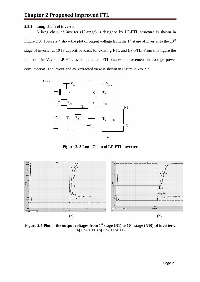
2.3.1 Long chain of inverter
A long chain of inverter (10-stage) is designed by LP-FTL structure is shown in
Figure 2.3. Figure 2.4 show the plot of output voltage from the 1st stage of inverter to the 10
th
stage of inverter at 10 fF capacitive loads for existing FTL and LP-FTL. From this figure the
reduction in VOL of LP-FTL as compared to FTL causes improvement in average power
consumption. The layout and av_extracted view is shown in Figure 2.5 to 2.7.
Figure 2. 3 Long Chain of LP-FTL inverter
Figure 2.4 Plot of the output voltages from 1st stage (N1) to 10
th stage (N10) of inverters.
(a) For FTL (b) For LP-FTL
TP2
TN
VDD
IN
N1
VDD
CLK
CL C
L
N2
TR
TP2
TN T
R
TP1
TP1
(a) (b)

Chapter 2 Proposed Improved FTL
Page 22
(a)
(b)
Figure 2.5 (a) Layout of FTL inverter (10-stage) (b) av_extracted view
(a)
(b)
Figure 2. 6 (a) Layout of LP-FTL inverter (10-stage) (b) av_extracted view

Chapter 2 Proposed Improved FTL
Page 23
Table 2.1 shows the average power (Pavg), average values of propagation delays (tp),
and power delay product (PDP) comparison of LP-FTL and the existing FTL in [15] for 10 fF
capacitive loads at 100 MHz. The LP-FTL structure provides reduction in power
consumption due to reduction in VOL. The power consumption by LP-FTL structure is 42.8%
less than that of existing FTL and it provides an area overhead of 24.4%.
Table 2. 1 Post Layout Simulation results comparison between FTL, LP-FTL in terms
of power, delay and area (10-inverter chain)
Logic
Family
Pavg
(µW)
tp
(ns)
Area
(µm²)
PDP
(µW*ns)
FTL [15] 271 800 221 216
LP-FTL 155 950 275 147
Chapter 2 Proposed Improved FTL
Page 24
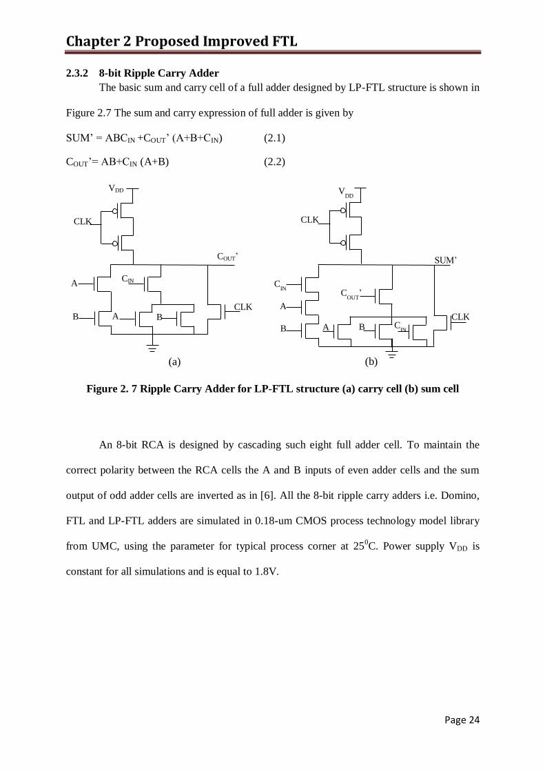
2.3.2 8-bit Ripple Carry Adder
The basic sum and carry cell of a full adder designed by LP-FTL structure is shown in
Figure 2.7 The sum and carry expression of full adder is given by
SUM’ = ABCIN +COUT’ (A+B+CIN) (2.1)
COUT’= AB+CIN (A+B) (2.2)
Figure 2. 7 Ripple Carry Adder for LP-FTL structure (a) carry cell (b) sum cell
An 8-bit RCA is designed by cascading such eight full adder cell. To maintain the
correct polarity between the RCA cells the A and B inputs of even adder cells and the sum
output of odd adder cells are inverted as in [6]. All the 8-bit ripple carry adders i.e. Domino,
FTL and LP-FTL adders are simulated in 0.18-um CMOS process technology model library
from UMC, using the parameter for typical process corner at 250C. Power supply VDD is
constant for all simulations and is equal to 1.8V.
VDD
VDD
CLK
CLK
SUM’
CLK
CLK
A
B
A
B
B
CIN C
IN
A
CIN
COUT’
COUT
’
A
B
(a) (b)
Chapter 2 Proposed Improved FTL
Page 25
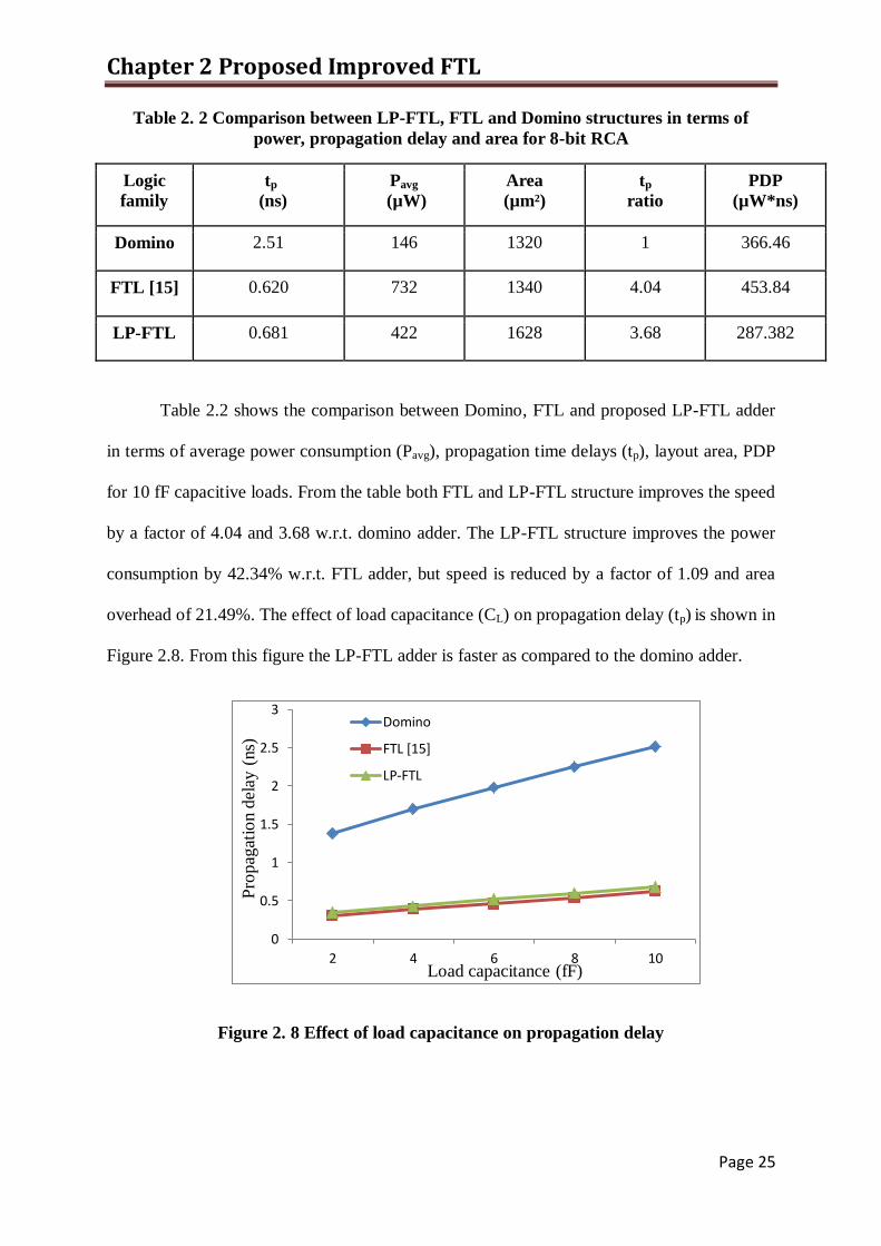
Table 2. 2 Comparison between LP-FTL, FTL and Domino structures in terms of
power, propagation delay and area for 8-bit RCA
Logic
family
tp
(ns)
Pavg
(µW)
Area
(µm²)
tp
ratio
PDP
(µW*ns)
Domino 2.51 146 1320 1 366.46
FTL [15] 0.620 732 1340 4.04 453.84
LP-FTL 0.681 422 1628 3.68 287.382
Table 2.2 shows the comparison between Domino, FTL and proposed LP-FTL adder
in terms of average power consumption (Pavg), propagation time delays (tp), layout area, PDP
for 10 fF capacitive loads. From the table both FTL and LP-FTL structure improves the speed
by a factor of 4.04 and 3.68 w.r.t. domino adder. The LP-FTL structure improves the power
consumption by 42.34% w.r.t. FTL adder, but speed is reduced by a factor of 1.09 and area
overhead of 21.49%. The effect of load capacitance (CL) on propagation delay (tp) is shown in
Figure 2.8. From this figure the LP-FTL adder is faster as compared to the domino adder.
Figure 2. 8 Effect of load capacitance on propagation delay
0
0.5
1
1.5
2
2.5
3
2 4 6 8 10
Domino
FTL [15]
LP-FTL
Load capacitance (fF)
Pro
pag
atio
n d
elay
(ns)

Chapter 2 Proposed Improved FTL
Page 26
2.3.3 LFSR
In order to explain the usefulness of proposed LP-FTL in pipelined circuit, we
designed a LFSR circuit as shown in Figure 2.9. The LP-FTL flip-flop shown in Figure 2.10 is
constructed from two cascaded LP-FTL latch controlled by the CLK and CLK’. The structure
of LP-FTL latch is shown in Figure 2.11. The XNOR-gate is also designed by using proposed
LP-FTL structure controlled by CLK.
Figure 2. 9 LFSR using LP-FTL flip-flop
Figure 2. 10 Positive edge triggered D flip-flop
X4
CLK CLK’ CLK CLK’ CLK CLK’ L
P-F
TL
flip-flo
p
D X1 Q
D Q
D Q
X2 X3
CLK
LP
-FT
L flip
-flop
LP
-FT
L flip
-flop
X4
LP-FTL flip-flop
D0 Q0 D1 Q1
CLK CLK
Q1’ Q0’
D Q
CLK
LP-FTL
Latch
CLK’
LP-FTL Latch

Chapter 2 Proposed Improved FTL
Page 27
Figure 2. 11 D-latch using LP-FTL
2.3.3.1 Operation of D-latch
The circuit diagram of D-latch by using LP-FTL structure is shown in Figure 2.11. The
operation of D-latch as follows. During the reset phase i.e. when CLK =1, TR turned on, both
the output node Q and Q’ holds their last state. During evaluation phase i.e. when CLK =0 TR
turned off, depending upon D value Q and Q’ are updated.
Suppose when CLK=0 and D=1,
(i) if in the last state Q=0 and Q’=1, then node Q charged to VDD through TP3 and TP4, since
now D=1 and Q=1, hence the transistor TN1 and TN5 are turned on as a result node Q’ will
evaluates to a logic low i.e. VOL.
Two cascaded FTL latch forms a positive edge triggered D-flip flop as shown in Figure
2.10. When CLK=0, the 1st LP-FTL latch is evaluated at the same time 2
nd LP-FTL latch holds
the last state. The input D is latched at the output of 1st FTL- latch. When CLK goes from 0 to
1, the 2nd
FTL latch is in evaluation phase the previously latched D value comes at the output
of 2nd
LP-FTL latch.
CLK
Q
D D’
Q’
VDD
VDD
Q’
Q
TP1
TP3
TP2
TP4
TR CLK
TN1
TN2
TN3
T
N4
TN5
TN6
CLK

Chapter 2 Proposed Improved FTL
Page 28
2.3.3.2 Simulation Results of LFSR
The average power consumption and propagation delay of LFSR is shown in Table
2.3. The proposed LP-FTL structure consumes less dynamic power as compared to existing
FTL. The waveforms at X1, X2, X3, X4 after every clock pulse is shown in Figure 2.12. The
transient power is also shown in Figure 2.12.
Table 2. 3 Power and propagation Delay Comparison between FTL and LP-FTL for
LFSR
Logic
family
Pavg
(µW)
tp
(ns)
FTL 349 5.167
Proposed
LP-FTL
196 5.290
Figure 2. 12 Output wave form at the X1, X2, X3, X4 of LFSR and total power

Chapter 2 Proposed Improved FTL
Page 29
2.4 HS-FTL Structure In order to improve the speed of proposed LP-FTL structure the reset transistor TR is
connected to VDD/2 as shown in Figre2.13 (a). The operation of this circuit is as follows,
when CLK =1, the output node (OUT) will charges to the threshold voltage VTH. During
evaluation phase according to input value the output node only makes partial transition from
VTH to VOH or VOL. Since during evaluation phase the output node (OUT) only makes partial
transitions, this improves propagation delay. An inverter designed by using HS-FTL is shown
in Figure 2.13 (b).
Figure 2. 13 (a) Proposed modified HS-FTL. (b) HS-FTL inverter
TP
VDD
A
CLK TP
VDD
In 1 OUT (In 1, In 2 … In N)
PDN I
n N
In 2
CLK
TR
TN
CLK
Y= A’
VDD/2
CLK
TR
VDD
/2
(a) (b)
Chapter 2 Proposed Improved FTL
Page 30
2.5 Performance analysis of HS-FTL The performance analysis of the HS-FTL structure is carried out by designing various
cascaded combinational circuits. We have designed a long chain of inverter (10-stage), 8-bit
RCA by using HS-FTL structure. We have used 0.18-um CMOS process technology model
library from UMC, using the parameter for typical process corner at 25 0C. Power supply VDD
is constant for all simulations and is equal to 1.8V. Circuits are simulated in HSPICE
simulator.
Figure 2. 14 Plot of the output voltages from 1st stage (N1) to 10th stage (N10) of
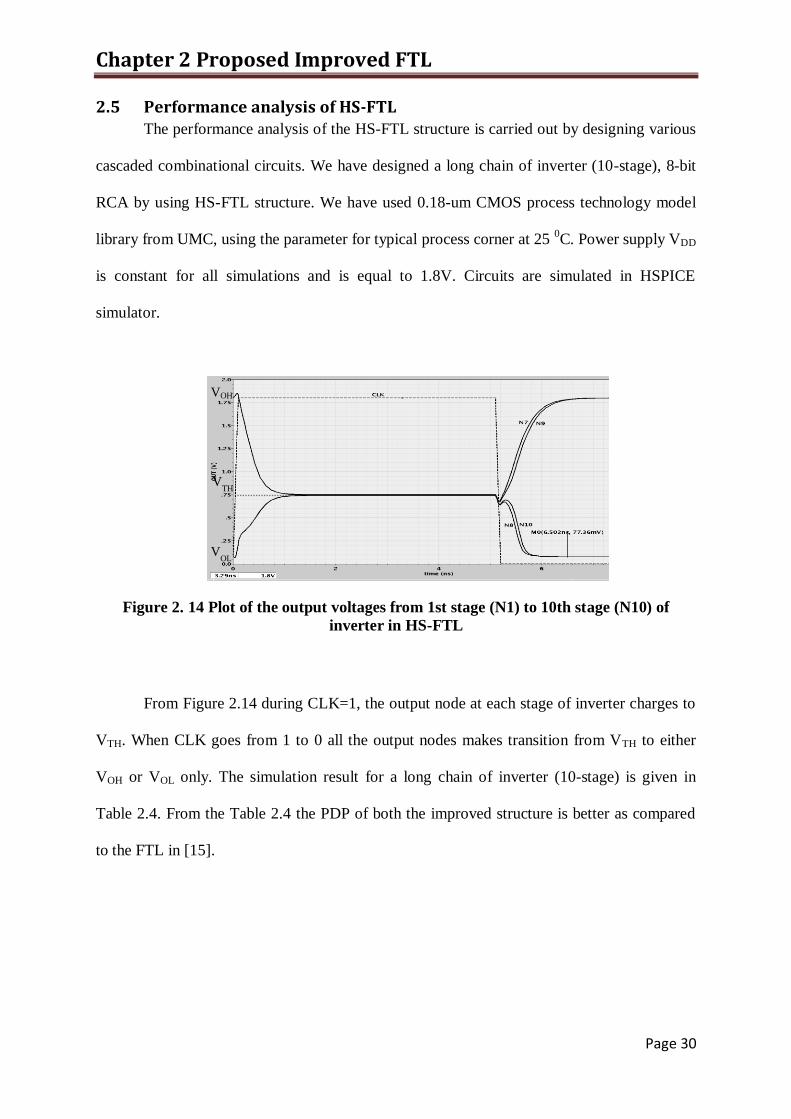
inverter in HS-FTL
From Figure 2.14 during CLK=1, the output node at each stage of inverter charges to
VTH. When CLK goes from 1 to 0 all the output nodes makes transition from VTH to either
VOH or VOL only. The simulation result for a long chain of inverter (10-stage) is given in
Table 2.4. From the Table 2.4 the PDP of both the improved structure is better as compared
to the FTL in [15].
VOH
VOL
VTH

Chapter 2 Proposed Improved FTL
Page 31
Table 2. 4 Simulation results comparison between FTL, LP-FTL and HS-FTL in terms
of power, delay (10-inverter chain)
Logic family Pavg
(µW)
tp
(ns)
PDP
(µW*ns)
FTL in [15] 270 0.725 195.75
Proposed LP-FTL 152 0.830 126.16
Proposed HS-FTL 290 0.538 156.02
Table 2. 5 Simulation results for an 8-bit RCA designed by proposed FTL structure and
the existing FTL structure [15]
Logic family Pavg
(µW)
tp
(ns)
PDP
(µW*ns)
FTL in [15] 732 0.620 453.84
LP-FTL 422 0.681 287.382
HS-FTL 735 0.430 316.05
Table 2.5 shows average power consumption, propagation delay time (tp), and power delay
product (PDP) of existing FTL structure in [15], LP-FTL and HS-FTL structure. The
proposed HS-FTL structure achieves a speed up factor of 1.58 with respect to LP-FTL
structure and 1.44 with respect to existing FTL structure. The power delay product of both
the proposed structures are better as compared to the existing FTL structure. The PDP
improves due to reduction of power in LP-FTL and reduction of average propagation delay in
HS-FTL structure.

Page 32
CHAPTER 3
DESIGN OF 8-BIT
RCA
Chapter 3 RCA Design
Page 33
3.1 Introduction
The basic design flow of an analog IC design, together with Cadence tool is shown in
Figure 3.1. A schematic view of circuit is created first by using Cadence composer schematic
editor. Then the circuit is simulated using cadence analog design environment. Different
simulators like spectre or Hspice are used. Then layout of schematic is created by using
Virtuoso Layout Editor.
The resulting layout is then subjected to Design Rule Check (DRC), which is some
geometric rules dependent on the technology. Electrical rule check (ERC) is then performed
for electrical errors like shorts. Then the layout compared with circuit schematic by
performing Layout Versus Schematic (LVS) check, to ensure that the intended functionally is
implemented.
Finally, a net list including parasitic resistance and capacitance extracted. The
simulation of this spice netlist is called as post Layout Simulation. Once the functionality of
layout is verified the final layout is converted to certain standard file formats like GDSII
depending upon foundry.

Chapter 3 RCA Design
Page 34
Figure 3.1 Analog IC design Flow
Specification
Schematic Entry
Simulation
DRC Check
LVS Check
Functional Check
Timing Check
Power Analysis
GDS II
Fabrication
Cadence Tool
Circuit Level
Design
Layout
Post-layout
Simulation
Composer
Spectre
Virtuoso
Spectre

Chapter 3 RCA Design
Page 35
3.2 8-bit RCA Design and Analysis
The schematic of 8-bit RCA by using LP-FTL structure and pre-layout simulation
results are discussed in chapter 2. In this section the layout issues and performance analysis
of 8-bit RCA is done by using 0.18-um CMOS process technology library from UMC.
3.2.1 Layout
The layout of a 1-bit full adder cell is given in Figure 3.2 designed by the sum and
carry cell discussed in chapter 2. The placing of transistors is critical in getting the most
compact design. Also, it is important to make sure that all important nodes should accessible
for routing. After the placing of transistors, the next step is to make the necessary routing
connections. The 8-bit RCA designed by using eight such cells in cascade. The layout of 8-bit
RCA is shown in Figure 3.3.
Figure 3.2 Layout of LP-FTL Full Adder

Chapter 3 RCA Design
Page 36
Figure 3.3 Layout of 8-bit Ripple Carry Adder

Chapter 3 RCA Design
Page 37
3.2.2 Creating I/O pins
After completion of layout the input and output pins which are present in schematic
are added to layout along with VDD and GND.
3.2.3 DRC
DRC is used to check all process-specific design rules. There are process specific
design rules which describe how closely the layers can be placed together. These rules
provide the minimum requirement to avoid failure of circuit due to fabrication fault. If the
layout is done perfectly then it shows no DRC error as in Figure 3.4.
Figure 3.4 DRC run window
3.2.4 LVS
The comparison between layout and schematic is performed by LVS check. If all the
connections and components in schematic and layout are matched properly, then this LVS
run shows that the schematic and layout matched, as shown in Figure 3.5.
Figure 3.5 LVS run window

Chapter 3 RCA Design
Page 38
3.2.5 Post Layout Simulation
The parasitic resistance and capacitance of layout is extracted by performing RCX
extraction, which is called as av_extracted view. The av_extracted view of 8-bit RCA is
shown in Figure 3.6. After generation of av_extracted view post-layout simulation is
performed. A configure window as shown in Figure 3.7 is generated to do post-layout
simulation. The power and timing analysis of post layout simulation is given in Table 3.
Figure 3.6 av_extracted view of 8-bit Ripple Carry Adder

Chapter 3 RCA Design
Page 39
Figure 3.7 configure window of 8-bit RCA for av_extracted view
Table 3 Performance summary of Proposed LP-FTL 8-bit RCA
Sl.no. Parameter Values
1 Supply Voltages 1.8 V
2 Average Power 436 µW
3 Propagation Delay 450 ps
4 Area 1628 µm²
5 Technology 0.18 µm CMOS
6 Technology Library UMC

Chapter 3 RCA Design
Page 40
3.2.6 GDSII
The GDS II window is shown is shown in Figure 3.8. The final layout can be further
instanced in icfb environment along with pad rings to export final GDS II file for fabrication.
Figure 3.8 GDS II window

Page 41
CHAPTER 4
NOISE ANALYSIS

Chapter 4 Noise analysis
Page 42
4.1 Introduction
Noise is defined as a pulse or glitch that appears at the inputs of dynamic gates and
discharges the dynamic nodes [17]. Continuous scaling of CMOS technology and increase in
circuit complexity are making the role of noise in deep submicron digital circuits more
important [18]. The main reason for its importance is,
(i) Scaling of threshold voltages
(ii) Increasing interconnect densities
(iii) High frequency of operation
Noise is used to designate any phenomenon that causes voltage at non switching node
to deviate from its nominal value [19]. Noise has always been an issue for analog circuits.
One of the reasons behind the popularity of digital systems as compared to analog system
was their inherent noise immunity. Noise immunity in digital dynamic circuits is becoming a
major issue with the progress of advanced VLSI technology. Furthermore, with the
continuous scaling of CMOS technologies, signal integrity and noise issue have become a
metric of comparable importance to power, performance and area. Static CMOS circuits can
achieve highest noise margin because at steady state output nodes are always connected to
either VDD or GND, but this is not possible in dynamic circuits due to possibilities floating
nodes which makes dynamic circuit more susceptible to noise. If a dynamic node stores its
value relatively for a long time, noise current can discharge the capacitor responsible for
holding logic level at dynamic node leading to functional failure. Therefore, the analysis of
effect of noise in dynamic circuits is very important.

Chapter 4 Noise analysis
Page 43
4.2 Noise Sources
The various sources of noise in deep submicron regions are crosstalk noise due to
capacitive coupling between neighboring inter-connects, small variation in nominal supply
voltage values, leakage current and fluctuations in device parameters due to process variation
[20]. Among the various sources of noise, the sub-threshold leakage current is the most
critical because it exponentially increases with continuous scaling of MOS transistor
dimension [11]. Due to technology scaling the supply voltage is scaled down in each new
technology; at the same time threshold voltage VTH of transistor is also scaled down to
achieve high performance that leads to continuous increase in sub-threshold leakage current
[11]. The leakage current is also increased due to continuous reduction in gate oxide
thickness. Therefore, the design of efficient noise tolerant circuit is an important issue in
present day VLSI design.
4.2.1 Type of Noise
(a) Power supply noise: It refers to noise appearing on the on-chip power and ground
distribution network produced by the current demand of the switching circuits.
(b) Circuit noise: It includes noise propagates onto an evaluation node from the driving
gate or charge sharing effects onto the output of driving gates.
(c) Coupling or Crosstalk noise: It refers to noise appearing as a result of capacitive or
inductive coupling between interconnects or as a result of poor impedance matching
between the device and interconnect. The effect of crosstalk noise becomes
increasingly significant with the growing interconnect aspect ratio[17], that lead to the
larger fraction of the wire capacitance being due to lateral coupling capacitance

Chapter 4 Noise analysis
Page 44
4.3 Logic Failure Due to Noise
The improved LP-FTL structure described in chapter-2 is less noise tolerant because
the switching threshold which is only depends upon transistors in the PDN block. The noise
tolerance of LP-FTL can be improved by increasing the threshold voltage of transistor in
PDN. Let a noise pulse of amplitude VN and width TN appears at the gate of TN1 as shown in
Figure 4.1. During evaluation phase, when VN exceeds the VTH of TN1, it causes TN1 to ON for
a short interval of time causing a glitch at the output node. This glitch at the output node can
be avoided by raising the threshold voltage of TN1.
Figure 4.1 Noise at the Input of LP-FTL Inverter
In this chapter several design techniques are described to improve the noise tolerant of
LP-FTL. All the noise tolerance circuit is based upon raising the source voltage of PDN
[21].We have designed inverter, 2-input NAND and 2-input NOR gate whose noise tolerant
is better as compared to logic gates designed by LP- FTL structure. The noise robustness of
the LP-FTL is analyzed by using ANTE metric.
CLK=0
TR
TN1
CLK=0 T
P1
TP2
VDD
TN
VN
Noise
OUT

Chapter 4 Noise analysis
Page 45
4.4 Noise Tolerant Circuit Techniques
All the noise tolerant circuit techniques are based on the principle of increasing the
threshold voltage of transistors in the PDN. The increase in threshold voltage of NMOS
transistors leads to reduction in sub-threshold leakage current [11]. Sub-threshold leakage
current (I subth) is the drain to source leakage current when transistor is OFF and is given by
[11]
)1.4(1
'01
T
DSDSVSVthVGSV
T v
V
vm
subth eeAI
Where
T
th
v
v
T
eff
ox eeVL
WCA
8.12'
0
VTH0 = Zero bias Threshold Voltage
VT = KT/q is the thermal Voltage
η = DIBL coefficient
Cox = Gate oxide Thickness
µ0 = Zero bias mobility
m = subthreshold swing coefficient

Chapter 4 Noise analysis
Page 46
4.4.1 Transistor stacking technique
In stacked technique a single NMOS transistor is replaced by one or more series
connected NMOS transistor. The stacked transistor reduces the sub-threshold leakage
current as follows,
(i) It increases the source potential (VS) of TN1, as a result its gate to source voltage (VGS)
reduces that leads to reduction in sub-threshold leakage current (I subth).
(ii) Due to increase in VS causes VTH of TN1 to increase as a result sub-threshold leakage
current also reduces.
(iii) Due to reduction in VS, VDS reduces as a result VTH increases which leads to reduction
in sub-threshold leakage.
In Figure 4.2 (a) the stacked transistor TS is used in series with TN1. Similarly for the
2-input NAND gate shown in Figure 4.2 (b) the two stacked transistor TS1 and TS2 are in
series with TN1 and TN2 respectively These stacked transistor increases VTH of TN1 and TN2 as
a result noise tolerance increases as compared to LP-FTL.
Figure 4.2 (a) Stacked Transistor inverter (b) Stacked Transistor NAND2
VDD
A
Y= A’
TS
TN1
TR
CLK
TP2
CLK
TP1
A
Y= (AB)’
B
TR
TN1
TN2
TS2
TS1
CLK
VDD
TP1
TP2
CLK
(a) (b)

Chapter 4 Noise analysis
Page 47
4.4.2 Triple Transistor technique
A 2-input NAND and NOR gate designed by this technique is shown in Figure 4.3. In
this technique one additional PMOS transistor is used along with stacked transistor. The
PMOS transistors (TP3) further increases the source voltage of TN1 along with the stacked
transistor (TS1). Similarly the threshold voltage of TN2 is increased by TP4 and TS2 In this
technique the reduction in sub-threshold leakage current is more as compared to stacked
transistor technique; as a result this circuit is more noise tolerant as compared to stacked
technique.
Figure 4. 3(a) Triple transistor NAND2 (b) Triple transistor NOR2
TN2
TS2
CLK
TP2
Y= (A+B)’
TR
VDD
A
Y= (AB)’
B
TR
TN1
TN2
TS2
TS1
CLK
TP1
TP2
CLK
A
CLK
TP1
VDD
TN1
TS1
TP3
TP3
TP4
TP4
B

Chapter 4 Noise analysis
Page 48
4.5 Simulation Results and comparison
The noise robustness of various noise tolerant techniques is analyzed by using ANTE
(average noise threshold energy) metric in [22]. ANTE is defined as the average input noise
energy that the circuit can tolerate..
4.5.1 Noise Immunity Curve
Noise immunity curves represent the robustness of dynamic logic circuits. This noise
immunity curve [22] is the locus of noise amplitude (VN) and width (TN) combinations that
cause the output of a logic gates switch as shown in Figure 4.4 (a). All the points on and
above this curve represents the noise pulses that will change the output of logic gate from its
desired value. The circuit with noise immunity curve given by Cimm2 is more robust than one
with Cimm1.
4.5.2 Noise injection Circuit (NIC)
For measuring the noise immunity of various noise tolerant circuits noise pulses are
injected to the input logic gates. Generally NIC circuit [17] is used to inject noise pules of
desired amplitude (VN) and width (TN) at the input of various logic gates as shown in Figure
4.4 (b). NIC are distributed throughout the chip to inject noise pulses. The NIC circuit is
used to produce a glitch at the output of a gate by staggering its inputs in time. The noise-
pulse width (TN) produced by NIC is controlled by VC and the amplitude of noise pulse (VN)
is controlled by the supply voltage of final inverter VDD, n. so by varying VC and VDD, n
various amount of noise can be injected at the input of logic gates.

Chapter 4 Noise analysis
Page 49
Figure 4.4 (a)Noise immunity curve [22] (b) NIC [17]
4.5.3 ANTE
Noise pulses with high amplitude and long duration causes un-recoverable logic error
in FTL. The noise tolerant is analyzed by using ANTE metric. ANTE is defined as the
average input noise energy that the circuit can tolerate. The pulse energy is defined as energy
dissipated in a 1Ω resistor subject to a voltage wave form of amplitude VN and TN.
)2.4()(2
NN TVEANTE
Where E () denotes the expectation operator.
VDD, n
VC
Error Free
Noise Pulse Width TN
(s)
Nois
e A
mpli
tude
VN
(
V)
Cimm1
Cimm2

Chapter 4 Noise analysis
Page 50
4.5.4 Noise tolerance analysis for Inverter
Figure 4.5 shows the noise immunity curves for inverter designed by LP-FTL and
stacked transistor technique for various VN and TN using 0.18-um CMOS process technology
model library from UMC, using the parameter for typical process corner at 250
C. Since the
stacked transistor reduces the sub-threshold leakage current, the inverter designed by stacked
transistor technique is more robust than LP-FTL. Table 4.1 shows the leakage power and
ANTE comparison for the inverter. The stacked transistor technique improves the ANTE by
1.54X.
Figure 4.5 Noise immunity curves for inverter
Table 4. 1 Performance comparison for inverter at 180 nm Technology
Techniques P leakage
(pW)
tp
(ps)
ANTE
(v2*ns)
LP-FTL 261 80 0.298
Stacked
Transistor
147 83 0.460
0
0.2
0.4
0.6
0.8
1
1.2
0.1 0.2 0.4 0.6 0.8 1
LP-FTLStacked LP-FTL
Noise Pulse Width (ns)
N
ois
e P
uls
e A
mp
litu
de
(V)

Chapter 4 Noise analysis
Page 51
4.5.5 Noise tolerance analysis for NAND2
The noise immunity curves for a 2-input NAND gate designed by LP-FTL structure,
stacked transistor and triple transistor technique is shown in Figure 4.6 for VDD=1.8V. These
curves are obtained by applying the noise pulses to the input of NAND gate generated from
NIC. The noise pulse width (TN) is kept fixed while the noise amplitude is increased until the
output node of NAND gate changes its logic state. This process is repeated for various TN
values. From Figure 4.6 we observe that the NAND gate designed by triple Transistor
technique is more robust compared to the original LP-FTL structure.
Figure 4.6 Noise immunity curves for NAND2
Table 4. 2 Performance comparison for 2-input NAND at 180 nm Technology
0
0.5
1
1.5
2
0.1 0.2 0.4 0.6 0.8 1
LP-FTLStacked LP-FTLTriple Transistor LP-FTL
Noise Pulse Width (ns)
N
ois
e P
uls
e A
mp
litu
de
(V)
Techniques ANTE
(v2*ns)
P leakage
(pW)
Delay
tp (ns)
ANTE/Delay
LP-FTL 0.439 147 0.083 5.289
Stacked
Transistor
0.593 136 0.085 6.976
Triple
Transistor
0.787 126 0.078 10.089

Chapter 4 Noise analysis
Page 52
Table 4.2 shows the performance comparison for a 2-input NAND gate. From the
table, it is observed that the triple transistor technique is improves ANTE by 1.79X over LP-
FTL structure and 1.32X over stacked transistor. The triple transistor technique reduces the
leakage power 14% as compared to the LP-FTL structure.
4.5.6 Noise tolerance analysis for NOR2
The noise immunity curves are shown in Figure 4.7. The performance analysis is
given in Table 4.3. From this table ANTE is improved by 2X w.r.t LP-FTL along with
reduction in leakage power.
Figure 4. 7Noise immunity curves for NOR2
Table 4. 3 Performance comparison for 2-input NOR at 180 nm Technology
0
0.2
0.4
0.6
0.8
1
1.2
1.4
0.1 0.2 0.4 0.6 0.8 1
LP-FTL
Triple Transistor Technique
Noise pulse Width (ns)
No
ise
Puls
e A
mpli
tude
(V)
Techniques ANTE
(v2*ns)
P leakage
(pW)
LP-FTL 0.258 147
Triple Transistor 0.521 126

Page 53
CHAPTER 5
CONCLUSIONS
&
FUTURE RESEARCH

Chapter 5 Conclusions
Page 54
5.1 Conclusions This thesis provides performance analysis of two improved FTL i.e. LP-FTL and HS-
FTL as discussed in chapter 2. Both these FTL structure provides improvement in speed as
compared domino CMOS. The RCA designed by LP-FTL structure is 3.68 times faster than
domino and reduces the average power consumption by 42% as compared to existing FTL.
This LP-FTL structure suffers from area overhead and increases in propagation delay as
compared to existing FTL. In order to improve propagation delay further, HS-FTL structure
is proposed. This HS-FTL structure improves speed without area overhead. Both these
improved FTL structure provides less PDP as compared to existing FTL.
The proposed noise tolerant techniques improves the noise immunity of LP-FTL and
demonstrated through various logic gates. We have used NAND2 and NOR2 logic gates to
study the noise tolerance analysis of LP-FTL. The various noise tolerance techniques like
stacked transistor and triple transistor techniques improves noise tolerant of LP-FTL structure
by 1.2X and 1.7X respectively.
5.2 Future Research This research can be further extended for performance optimization in terms of
power, speed, area and noise immunity.

Page 55
REFERENCES
[1] S .Mathew, M. Anders, R. Krishnamurthy, S. Borkar, “A 4 GHz 130 nm address
generation unit with 32-bit sparse-tree adder core,” IEEE VLSI Circuits Symp. ,
Honolulu, pp. 126-127, jun 2002.
[2] S. vangal, Y. Hoskote, D. Somasekhar, V. Erraguntla, J. Howard, G. Ruhl, V.
Veeramachaneni, D. Finan, S. Mathew, and N. Borkar, “A 5-GHz floating point multiply-
accumulator in 90-nm dual VT CMOS,” in Proc. IEEE Int. Solid-State Circuits Conf.,
San Francisco, pp. 334–335, Feb.2003.
[3] R.K. Krishnamurthy, S. Hsu, M. Anders, B. Bloechel, B. Chatterjee, M. Sachdev, S.
Borkar, “Dual Supply voltage clocking for 5GHz 130nm integer execution core,”
proceedings of IEEE VLSI Circuits Symposium, Honolulu, pp. 128-129Jun. 2002.
[4] Y.jiang, A. Al-sheraidah, Y. Wang, E.sha, J. Chung, A novel multiplexer based low-
power full adder, IEEE Trans. Circuits Syst.-II,vol. 52, pp. 345-348, 2004.
[5] S .Mathew, M. Anders, R. Krishnamurthy, S. Borkar, “A 4 GHz 130 nm address
generation unit with 32-bit sparse-tree adder core,” IEEE J. Solid State Circuits Vol.38
(5), pp. 689-695,2003.
[6] J.M. Rabaey, A. Chandrakasan, B. Nikolic, ‘Digital Integrated Circuits: A Design
perspective’ 2e Prentice-Hall, Upper saddle River, NJ, 2002.
[7] S. M. Kang, Y. Leblebici, ‘CMOS Digital Integrated Circuits: Analysis & Design’,
TATA McGraw- Hill Publication, 3e, 2003.
[8] N. Weste, K. Eshraghian, ‘Principles of CMOS VLSI Design, A systems perspective’,
Addision Wesley MA, 1988.
[9] J. P. Uyemura, ‘CMOS logic circuit design’, Kluwer Academic.

Page 56
[10] A.Devgan, “Efficient couple noise estimation for on-chip interconnects”, ICCAD97,
pp. 147-151,1997.
[11] K.S. Yeo, K. Roy, ‘Low- Voltage, Low-Power VLSI Subsystems’.
[12] K. Roy, S. Prasad, ‘Low-Power CMOS VLSI Circuit design’, A willey Interscience
Publication,2000.
[13] A.P. Chandrakasan and R.W. Broderson, ‘Low Power Digital CMOS Design,’
Kluwer Academic,1995.
[14] Mohamed I.Elmarsy and Abdellatif Bellaouar, “Low-Power digital VLSI Design
Circuits and Systems”, Kluwer Academic, 1995.
[15] V. Navarro-Botello, J. A. Montiel-Nelson, and S. Nooshabadi, “ Analysis of high
performance fast feedthrough logic families in CMOS,” IEEE Trans. Cir. & syst. II, vol.
54, no. 6, pp. 489-493, Jun. 2007.
[16] S. Nooshabadi and J. A. Montiel-Nelson, “Fast feedthrough logic: A high
performance logic family for GaAs,” IEEE Trans. Circuit Syst. I, Reg. Paper, vol. 51, no.
11, pp. 2189-2203, Nov.2004.
[17] G. Balamurugan and N. R. shanbhag, “The twin-transistor noise tolerant dynamic
circuit technique,” IEEE J. Solid-State Circuits, vol. 36, no. 2, pp. 273-280, Feb. 2001.
[18] K. L. shepard and V. Narayanan, “Noise in deep submicron digital design,” in Proc.
ICCAD, pp. 524-531,1996.
[19] K. L. shepard, “Design methodologies for noise in digital integrated circuits,” in Proc.
DAC’, pp. 94-99,1998.
[20] C. Murthy, “Process variation effects on circuitperformance: TCAD simulation of
256-Mbit technology,” IEEE Trans, Computer-Aided Designof integrated Circuits, vol.
16, pp. 1383-1389, Nov.1997.

Page 57
[21] I-Chyn Wey, Y-Gang Chen and An-Yeu Wu, “Design and analysis of Isolated Noise-
Tolerant Technique in Dynamic CMOS Citcuits,” IEEE Trans.on VLSI sys.,vol.16,
no.12, pp. 1708-1712, Dec.2008
[22] L. Wang and N. Shanbhag, “An energy-efficient noise-tolerant dynamic circuit
design,” IEEE Trans. Cir. & syst. II, vol. 47, pp. 1300-1306, Nov. 2000.


![Fabrikasi Dan Karakterisasi Pandu Gelombang Planar … · implantation, dan ion exchange (pertukaran ion)[4]. Dalam teknik pertukaran ion, ion dari substrat dipertukarkan dengan ion](https://img.pdfslide.tips/doc/110x75/5b3f54c07f8b9a2f138bf310/fabrikasi-dan-karakterisasi-pandu-gelombang-planar-implantation-dan-ion-exchange.jpg)