Embed Size (px)
Citation preview
High speed, Low dropout, ±1% High output accuracy
CMOS Voltage Regulator with Dual output
VRD Series
Rev. E13-01
Analog Semiconductor IC
.......... Future of the analog world AnaSem
AnaSem
(IMPORTANT: Please check the last page for Genuine Product Labeling)
Website: www.anasemi.com Tel: +852-3590-8442 Email: [email protected]
安纳森安纳森安纳森安纳森
AnaSem 1
AnaSem
Rev. E13-01
Products Data Sheet
Analog Semiconductor IC
.......... Future of the analog world www.anasemi.com [email protected]
High speed, Low dropout, ±1% High output accuracy Dual CMOS Voltage Regulator
VRD Series
GENERAL DESCRIPTIONS
The VRD series are dual positive voltage regulators with high speed, low voltage dropout and high accuracy output achieved by low current consumption. Because each regulator is completely separated, the crosstalk between each regulator can be reduced. The output voltage is guaranteed within ±1% within the given temperature range by Vref controlling the temperature characteristic. It corresponds to the low ESR capacitor as an output stabilization capacitor. The charged ESR capacitor can be discharged with an internal switch by making the CE=VSS, as a result the VOUT quickly returns to the VSS level. To make the current capacity of the output transistor not exceeded, the over-current protection circuit is built in.
FEATURES
Output voltage range ······································································· Operating voltage range ·································································· High accuracy output voltage ··························································· Maximum output current ·································································· Dropout voltage ················································································ Low current consumption ·································································· High ripple rejection ························································································· Low ESR capacitor ························································································· Operating temperature range ·································································· Built-in over-current protector ································································ CL high-speed auto-discharge Built-in On/Off circuit Small package ·························································································
APPLICATIONS
Battery powered devices Cellular phone Digital / Video cameras
HALOGEN
RoHS COMPLIANCE
Portable games Handheld instruments
0.8V~5.0V (selectable with a step of 0.05V) 1.6V~6.0V ±1% (Vout=1.95V~ 5.0V) / ±20mV (Vout=0.8V~1.9V) 250mA / Channel Typ.90mV (output=3.0V, IOUT=100mA) Typ. 25µA / Channel Typ. 75dB at 1KHz 1.0 µF ceramic capacitor –40°C ~ +85°C Limit current : 300mA SOT-26 (2.9×2.8×1.1mm), LLP-6 (1.8×2.0×0.6mm)
AnaSem
2 .......... Future of the analog world www.anasemi.com [email protected]
Rev. E13-01 VRD Series
High speed, Low dropout, ±1% High output accuracy Dual CMOS Voltage Regulator
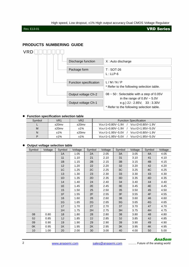
PRODUCTS NUMBERING GUIDE
Function specification selection table Symbol VR1 VR2 Function Specification
L ±20mv ±20mv VOUT1=0.80V~1.9V / VOUT2=0.80V~1.9V M ±20mv ±1% VOUT1=0.80V~1.9V / VOUT2=1.95V~5.0V N ±1% ±20mv VOUT1=1.95V~5.0V / VOUT2=0.80V~1.9V P ±1% ±1% VOUT1=1.95V~5.0V / VOUT2=1.95V~5.0V
Output voltage selection table
Symbol Voltage Symbol Voltage Symbol Voltage Symbol Voltage Symbol Voltage 1A 1.05 2A 2.05 3A 3.05 4A 4.05 11 1.10 21 2.10 31 3.10 41 4.10 1B 1.15 2B 2.15 3B 3.15 4B 4.15 12 1.20 22 2.20 32 3.20 42 4.20 1C 1.25 2C 2.25 3C 3.25 4C 4.25 13 1.30 23 2.30 33 3.30 43 4.30 1D 1.35 2D 2.35 3D 3.35 4D 4.35 14 1.40 24 2.40 34 3.40 44 4.40 1E 1.45 2E 2.45 3E 3.45 4E 4.45 15 1.50 25 2.50 35 3.50 45 4.50 1F 1.55 2F 2.55 3F 3.55 4F 4.55 16 1.60 26 2.60 36 3.60 46 4.60 1G 1.65 2G 2.65 3G 3.65 4G 4.65 17 1.70 27 2.70 37 3.70 47 4.70 1H 1.75 2H 2.75 3H 3.75 4H 4.75
08 0.80 18 1.80 28 2.80 38 3.80 48 4.80 0J 0.85 1J 1.85 2J 2.85 3J 3.85 4J 4.85 09 0.90 19 1.90 29 2.90 39 3.90 49 4.90 0K 0.95 1K 1.95 2K 2.95 3K 3.95 4K 4.95 10 1.00 20 2.00 30 3.00 40 4.00 50 5.00
VRD
Output voltage Ch-1
Discharge function
T : SOT-26 L : LLP-6
Package form
L / M / N / P * Refer to the following selection table.
Function specification
X : Auto discharge
08 ~ 50 : Selectable with a step of 0.05V in the range of 0.8V ~ 5.0V
e.g.) 2J : 2.85V, 33 : 3.30V * Refer to the following selection table.
Output voltage Ch-2
AnaSem
3 .......... Future of the analog world www.anasemi.com [email protected]
Rev. E13-01 VRD Series
High speed, Low dropout, ±1% High output accuracy Dual CMOS Voltage Regulator
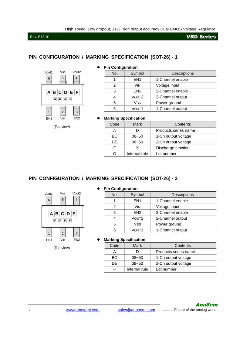
PIN CONFIGURATION / MARKING SPECIFICATION (SOT-26) - 1
PIN CONFIGURATION / MARKING SPECIFICATION (SOT-26) - 2
Pin Configuration No. Symbol Descriptions
1 EN1 1-Channel enable
2 VIN Voltage input
3 EN2 2-Channel enable
4 VOUT2 2-Channel output
5 VSS Power ground
6 VOUT1 1-Channel output
Marking Specification
Code Mark Contents
A D Products series name
BC 08~50 1-Ch output voltage
DE 08~50 2-Ch output voltage
F X Discharge function
G Internal rule Lot number
(Top view)
Vout1
Vin
Vss Vout2
EN2
1 2 3
4 6 5
EN1
A G G G G
B C D E F
Pin Configuration No. Symbol Descriptions
1 EN1 1-Channel enable
2 VIN Voltage input
3 EN2 2-Channel enable
4 VOUT2 2-Channel output
5 VSS Power ground
6 VOUT1 1-Channel output
Marking Specification
Code Mark Contents
A D Products series name
BC 08~50 1-Ch output voltage
DE 08~50 2-Ch output voltage
F Internal rule Lot number
(Top view)
Vout1
Vin
Vss Vout2
EN2
1 2 3
4 6 5
EN1
A F F F F
B C D E
AnaSem
4 .......... Future of the analog world www.anasemi.com [email protected]
Rev. E13-01 VRD Series
High speed, Low dropout, ±1% High output accuracy Dual CMOS Voltage Regulator
PIN CONFIGURATION / MARKING SPECIFICATION (LLP-6)
Marking Specification Code Mark Contents
A D Products series name
BC 08~50 1-Ch output voltage
DE 08~50 2-Ch output voltage
F X Discharge function
G Internal rule Lot number
Pin Configuration No. Symbol Descriptions
1 EN2 2-Channel enable
2 VIN Voltage input
3 EN1 1-Channel enable
4 VSS Power ground
5 VOUT1 1-Channel output
6 VOUT2 2-Channel output
EN1 EN2 Vin
Vout1 Vss Vout2
1 2 3
4 5 6
(Top view)
A
G G G
B C
D E F G
AnaSem
5 .......... Future of the analog world www.anasemi.com [email protected]
Rev. E13-01 VRD Series
High speed, Low dropout, ±1% High output accuracy Dual CMOS Voltage Regulator
BLOCK DIAGRAM
ABSOLUTE MAXIMUM RATINGS
Note :
※1) Power dissipation depends on conditions of mounting on boards. PCB dimension is 50mm×50mm×1.6mm.
TYPICAL APPLICATION CIRCUITS
Items Symbol Ratings Unit
Input voltage range VIN –0.3 ~ +7.0 V
Output current IOUT 500 mA
Output voltage range VOUT VSS –0.3 ~ VIN +0.3 V
Power dissipation ※1) SOT-26 PD 600 mW
LLP-6 PD 1000 mW
Operating temperature range TOPR –40 ~ +85 °C
Storage temperature range TSTG –55 ~ +125 °C
VIN
Vss
+
_
VOUT1
Voltage Reference
Over-current Protector
EN1
+
_ Voltage Reference
Over-current Protector
EN2
VOUT2
CL1 = 1µF
VOUT1
VIN VSS
CIN = 1µF
VOUT2
CL2 = 1µF
EN2
EN1
AnaSem
6 .......... Future of the analog world www.anasemi.com [email protected]
Rev. E13-01 VRD Series
High speed, Low dropout, ±1% High output accuracy Dual CMOS Voltage Regulator
ELECTRICAL CHARACTERISTICS
Items Symbol Conditions Min. Typ. Max. Unit Test circuit
Output voltage VOUT
VOUT+1.0V≦VIN≦6.0V
IOUT=30mA
Ta=–40°C ~ +85°C
VOUT≧1.95V VOUT ×0.99
VOUT VOUT ×1.01
V
1
VOUT≦1.90V –20 - +20 mV
Output current IOUT VIN≧VOUT+1.0V
0.9V≦VOUT≦1.15V - 250 - mA
1
1.2V≦VOUT≦1.65V - 250 - mA
1.7V≦VOUT≦2.25V - 250 - mA
2.3V≦VOUT≦2.85V - 250 - mA
2.9V≦VOUT≦3.45V - 250 - mA
3.5V≦VOUT≦4.05V - 250 - mA
4.0V≦VOUT≦5.00V - 250 - mA
Dropout voltage VDROP IOUT=100mA
0.9V≦VOUT≦1.15V - 580 910 mV
1
1.2V≦VOUT≦1.65V - 210 340 mV
1.7V≦VOUT≦2.25V - 130 205 mV
2.3V≦VOUT≦2.85V - 100 150 mV
2.9V≦VOUT≦3.45V - 90 137 mV
3.5V≦VOUT≦4.05V - 85 125 mV
4.1V≦VOUT≦5.00V - 80 115 mV
(Ta=25°C unless otherwise specified)
AnaSem
7 .......... Future of the analog world www.anasemi.com [email protected]
Rev. E13-01 VRD Series
High speed, Low dropout, ±1% High output accuracy Dual CMOS Voltage Regulator
ELECTRICAL CHARACTERISTICS (CONTINUED)
Items Symbol Conditions Min. Typ. Max. Unit Test circuit
Current consumption IDD VIN=VOUT+1.0V, VOUT=Open, IOUT=0mA - 50 80 µA 2
Standby current ISTB EN=VSS - 0.01 0.1 µA 2
Input voltage VIN 1.6 - 6.0 V 1
Load regulation ∆VOUT VIN=VOUT+1.0V, IOUT=0.1mA ~100mA - 10 40 mV 1
Line regulation ∆VOUT / ∆VIN•VOUT VOUT+1.0V≦VIN≦6.0V, IOUT=30mA - 0.01 0.1 %/V 1
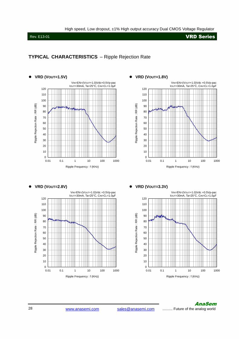
Ripple rejection Rr VIN=VOUT+1.0V, f=1KHz, ∆VRIP=0.5VP-P, IOUT=30mA - 75 - dB 3
Limit current ILIMIT EN=VIN 300 - - mA 1
Short circuit current ISHORT VIN=VOUT+1.0V, VOUT=0V - 40 - mA 1
Output voltage temperature coefficient
∆VOUT / ∆Ta•VOUT
VEN=VIN, IOUT=300mA Ta=–40°C ~ +85°C ±20 ppm
/°C 1
EN high level voltage VENH 1.2 - 6.0 V 1
EN low level voltage VENL - - 0.3 V 1
EN high level current IENH VEN= VIN –0.1 - 0.1 µA 1
EN low level current IENL VEN= VSS –0.1 - 0.1 µA 1
CL auto-discharge resistance RDIS VIN=6.0V, VOUT=4.0V, VEN= VSS - 160 - Ω 1
(Ta=25°C unless otherwise specified)
AnaSem
8 .......... Future of the analog world www.anasemi.com [email protected]
Rev. E13-01 VRD Series
High speed, Low dropout, ±1% High output accuracy Dual CMOS Voltage Regulator
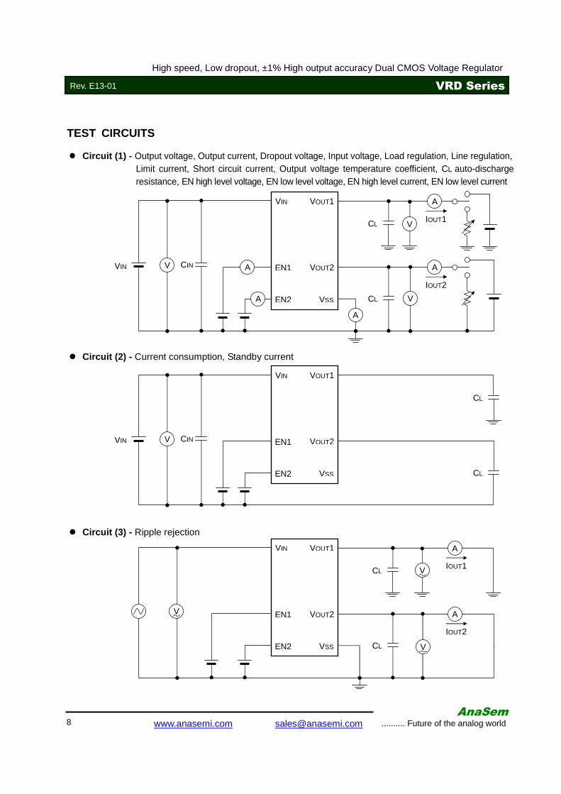
TEST CIRCUITS
Circuit (1) - Output voltage, Output current, Dropout voltage, Input voltage, Load regulation, Line regulation, Limit current, Short circuit current, Output voltage temperature coefficient, CL auto-discharge resistance, EN high level voltage, EN low level voltage, EN high level current, EN low level current
Circuit (2) - Current consumption, Standby current
Circuit (3) - Ripple rejection
VSS
VOUT1
EN1 VIN CIN A
CL V
VIN
VOUT2
EN2
A
V
A
A
IOUT2
A
CL IOUT1 V
VSS
VOUT1
EN1 VIN CIN
CL
VIN
VOUT2
EN2
V
CL
VSS
VOUT1
EN1 A
CL
VIN
VOUT2
EN2
IOUT2
A
CL IOUT1
V
V
V
AnaSem
9 .......... Future of the analog world www.anasemi.com [email protected]
Rev. E13-01 VRD Series
High speed, Low dropout, ±1% High output accuracy Dual CMOS Voltage Regulator
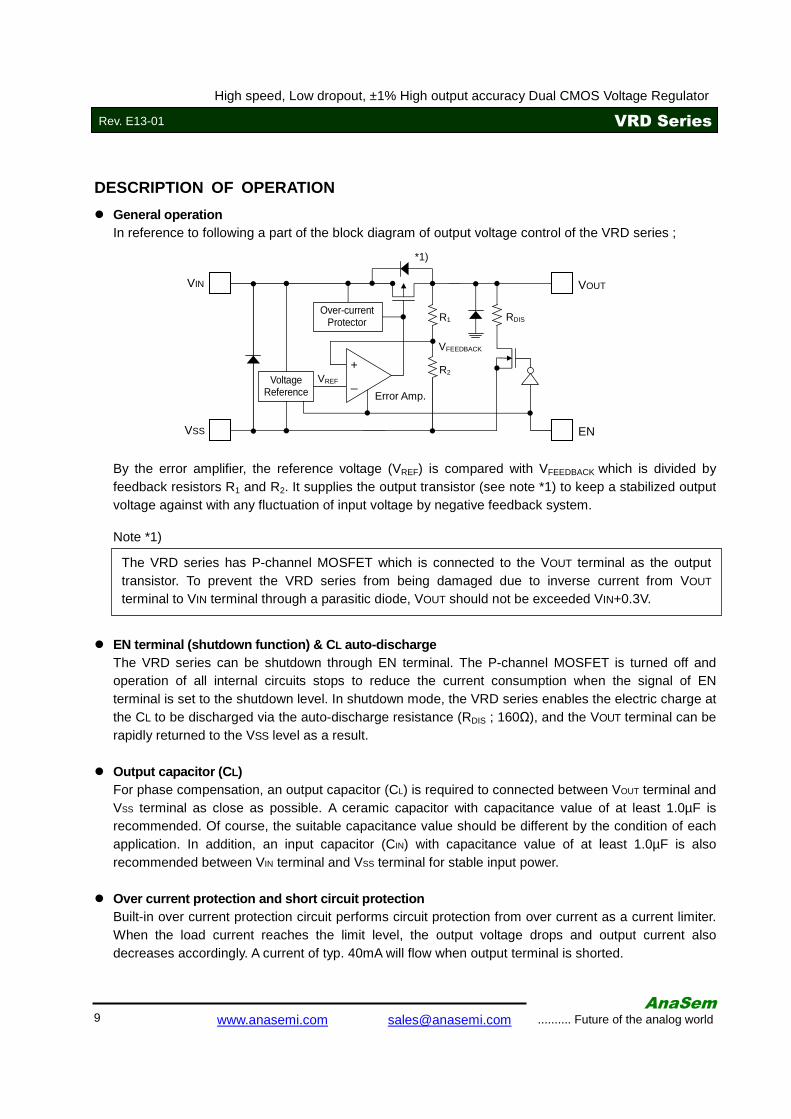
DESCRIPTION OF OPERATION
General operation In reference to following a part of the block diagram of output voltage control of the VRD series ;
By the error amplifier, the reference voltage (VREF) is compared with VFEEDBACK which is divided by feedback resistors R1 and R2. It supplies the output transistor (see note *1) to keep a stabilized output voltage against with any fluctuation of input voltage by negative feedback system. Note *1)
EN terminal (shutdown function) & CL auto-discharge The VRD series can be shutdown through EN terminal. The P-channel MOSFET is turned off and operation of all internal circuits stops to reduce the current consumption when the signal of EN terminal is set to the shutdown level. In shutdown mode, the VRD series enables the electric charge at the CL to be discharged via the auto-discharge resistance (RDIS ; 160Ω), and the VOUT terminal can be rapidly returned to the VSS level as a result.
Output capacitor (CL) For phase compensation, an output capacitor (CL) is required to connected between VOUT terminal and VSS terminal as close as possible. A ceramic capacitor with capacitance value of at least 1.0µF is recommended. Of course, the suitable capacitance value should be different by the condition of each application. In addition, an input capacitor (CIN) with capacitance value of at least 1.0µF is also recommended between VIN terminal and VSS terminal for stable input power.
Over current protection and short circuit protection
Built-in over current protection circuit performs circuit protection from over current as a current limiter. When the load current reaches the limit level, the output voltage drops and output current also decreases accordingly. A current of typ. 40mA will flow when output terminal is shorted.
VIN
VSS
+
_
VOUT
Voltage Reference
Over-current Protector
EN
VREF
Error Amp.
R2
R1
VFEEDBACK
*1)
The VRD series has P-channel MOSFET which is connected to the VOUT terminal as the output transistor. To prevent the VRD series from being damaged due to inverse current from VOUT terminal to VIN terminal through a parasitic diode, VOUT should not be exceeded VIN+0.3V.
RDIS
AnaSem
10 .......... Future of the analog world www.anasemi.com [email protected]
Rev. E13-01 VRD Series
High speed, Low dropout, ±1% High output accuracy Dual CMOS Voltage Regulator
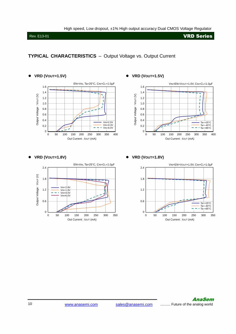
TYPICAL CHARACTERISTICS – Output Voltage vs. Output Current
VRD (VOUT=1.8V) VRD (VOUT=1.8V)
2.4
1.8
1.2
0.6
0 50 150 200 250 300 0
Out Current : IOUT (mA)
100 350 50 150 200 250 300 0
Out Current : IOUT (mA)
100 350
Ta=+25°C Ta=–40°C Ta=+85°C
VRD (VOUT=1.5V)
EN=VIN, Ta=25°C, CIN=CL=1.0µF
VRD (VOUT=1.5V)
VIN=EN=VOUT+1.0V, CIN=CL=1.0µF
Out
put V
olta
ge :
VO
UT (
V)
1.6
1.2
0.8
0.4
0
0.2
0.6
1.0
1.4
50 150 200 250 300 0
Out Current : IOUT (mA)
100 350 400 50 150 200 250 300 0
Out Current : IOUT (mA)
100 350 400
VIN=2.8V VIN=1.9V VIN=4.0V VIN=6.0V
Ta=+25°C Ta=–40°C Ta=+85°C
VIN=2.5V VIN=4.3V VIN=6.0V
Out
put V
olta
ge :
VO
UT (
V)
1.6
1.2
0.8
0.4
0
0.2
0.6
1.0
1.4
Out
put V
olta
ge :
VO
UT (
V)
2.4
1.8
1.2
0.6
0
EN=VIN, Ta=25°C, CIN=CL=1.0µF VIN=EN=VOUT+1.0V, CIN=CL=1.0µF
AnaSem
11 .......... Future of the analog world www.anasemi.com [email protected]
Rev. E13-01 VRD Series
High speed, Low dropout, ±1% High output accuracy Dual CMOS Voltage Regulator
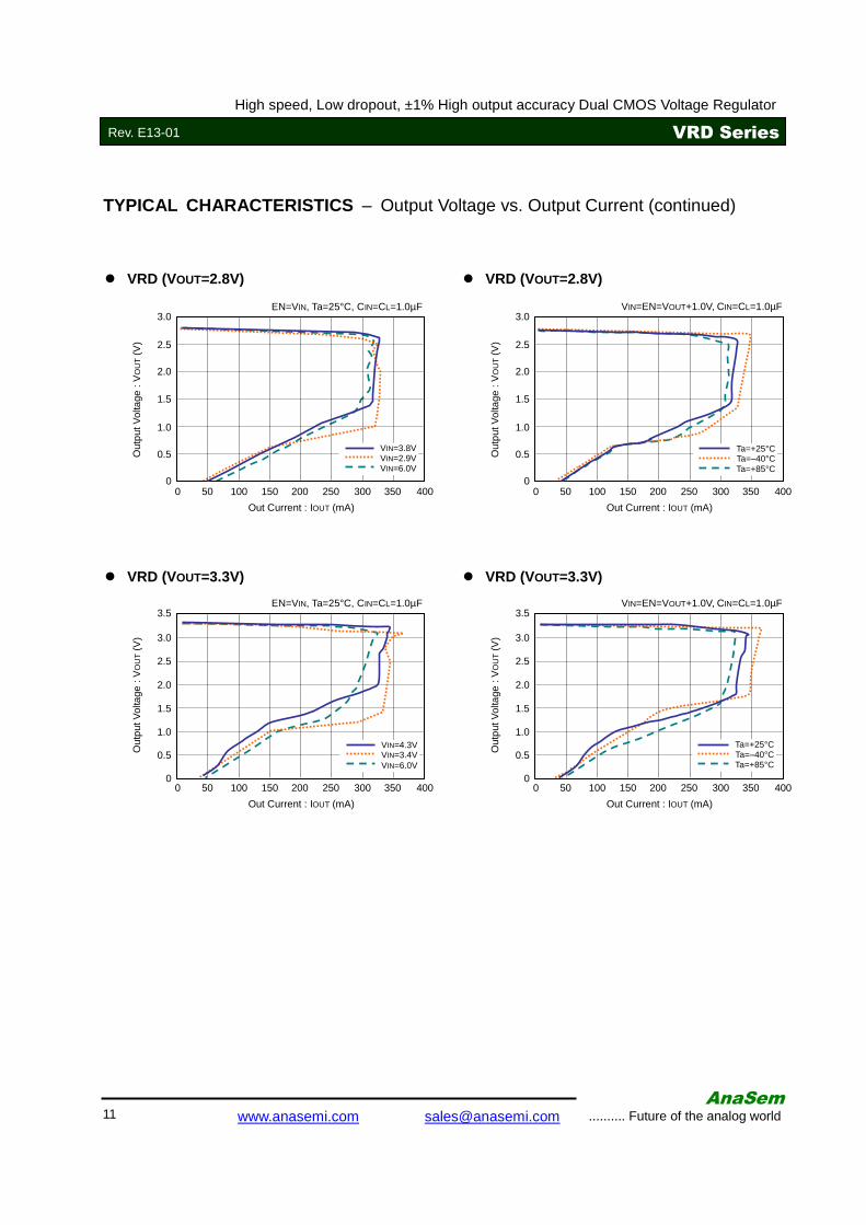
TYPICAL CHARACTERISTICS – Output Voltage vs. Output Current (continued)
VRD (VOUT=2.8V) VRD (VOUT=2.8V)
2.5
2.0
1.0
0
0.5
1.5
3.0
50 150 200 250 300 0
Out Current : IOUT (mA)
100 350 400 50 150 200 250 300 0
Out Current : IOUT (mA)
100 350 400
VIN=3.8V VIN=2.9V VIN=6.0V
VRD (VOUT=3.3V)
50 150 200 250 300 0
Out Current : IOUT (mA)
100 350 400
2.5
2.0
1.0
0
0.5
1.5
3.5
3.0
VRD (VOUT=3.3V)
50 150 200 250 300 0
Out Current : IOUT (mA)
100 350 400
VIN=4.3V VIN=3.4V VIN=6.0V
Ta=+25°C Ta=–40°C Ta=+85°C
Ta=+25°C Ta=–40°C Ta=+85°C
Out
put V
olta
ge :
VO
UT (
V) 2.5
2.0
1.0
0
0.5
1.5
3.0
Out
put V
olta
ge :
VO
UT (
V)
Out
put V
olta
ge :
VO
UT (
V)
2.5
2.0
1.0
0
0.5
1.5
3.5
3.0
Out
put V
olta
ge :
VO
UT (
V)
EN=VIN, Ta=25°C, CIN=CL=1.0µF VIN=EN=VOUT+1.0V, CIN=CL=1.0µF
EN=VIN, Ta=25°C, CIN=CL=1.0µF VIN=EN=VOUT+1.0V, CIN=CL=1.0µF
AnaSem
12 .......... Future of the analog world www.anasemi.com [email protected]
Rev. E13-01 VRD Series
High speed, Low dropout, ±1% High output accuracy Dual CMOS Voltage Regulator
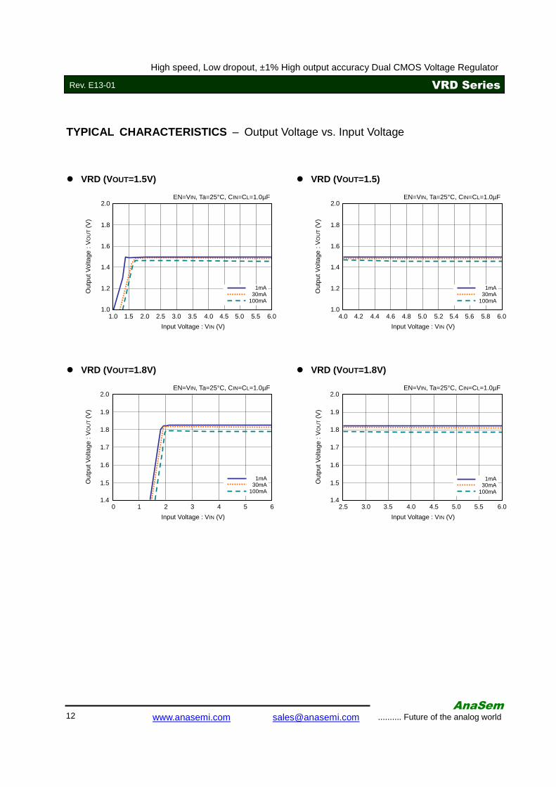
TYPICAL CHARACTERISTICS – Output Voltage vs. Input Voltage
VRD (VOUT=1.8V)
2 3 4 6 0
Input Voltage : VIN (V)
1.9
1.8
1.6
1.4
1.5
1.7
2.0
1 5
VRD (VOUT=1.8V)
3.5 4.0 5.0 6.0 2.5
Input Voltage : VIN (V)
3.0 5.5 4.5
1mA 30mA
100mA
VRD (VOUT=1.5V)
Out
put V
olta
ge :
VO
UT (
V)
2.5 3.5 4.5 6.0 1.0
Input Voltage : VIN (V)
1.8
1.4
1.0
1.2
1.6
2.0
1.5 5.0
VRD (VOUT=1.5)
1mA 30mA
100mA
2.0 3.0 4.0 5.5 4.6 5.0 5.4 6.0 4.0
Input Voltage : VIN (V)
4.2 5.6
1mA 30mA
100mA
4.4 4.8 5.2 5.8
1mA 30mA
100mA
Out
put V
olta
ge :
VO
UT (
V)
1.8
1.4
1.0
1.2
1.6
2.0
Out
put V
olta
ge :
VO
UT (
V) 1.9
1.8
1.6
1.4
1.5
1.7
2.0
Out
put V
olta
ge :
VO
UT (
V)
EN=VIN, Ta=25°C, CIN=CL=1.0µF EN=VIN, Ta=25°C, CIN=CL=1.0µF
EN=VIN, Ta=25°C, CIN=CL=1.0µF EN=VIN, Ta=25°C, CIN=CL=1.0µF
AnaSem
13 .......... Future of the analog world www.anasemi.com [email protected]
Rev. E13-01 VRD Series
High speed, Low dropout, ±1% High output accuracy Dual CMOS Voltage Regulator
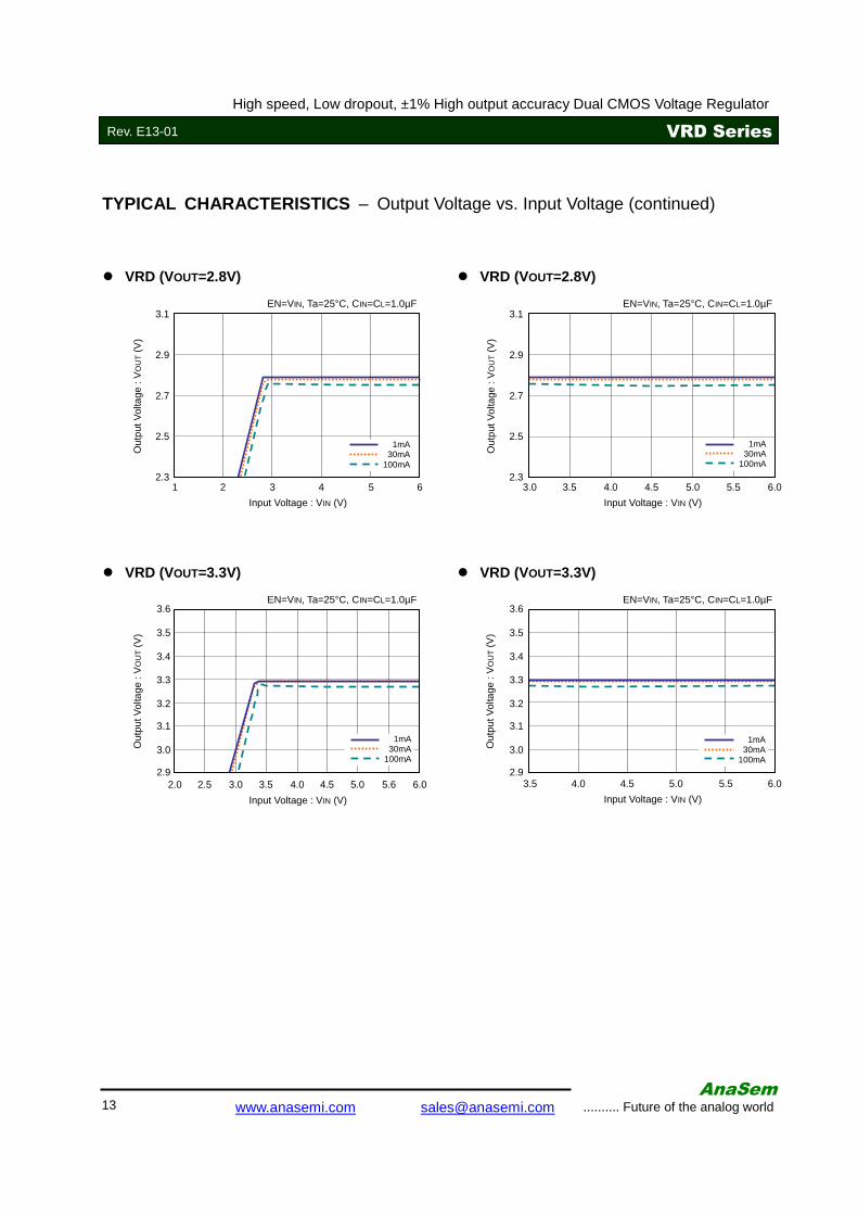
TYPICAL CHARACTERISTICS – Output Voltage vs. Input Voltage (continued)
VRD (VOUT=2.8V)
Out
put V
olta
ge :
VO
UT (
V)
3 4 6 1
Input Voltage : VIN (V)
2 5
VRD (VOUT=2.8V)
4.0 4.5 5.0 6.0 3.0
Input Voltage : VIN (V)
3.5 5.5
2.7
2.3
2.5
3.1
2.9
VRD (VOUT=3.3V)
3.5 4.5 6.0 2.0
Input Voltage : VIN (V)
3.0 5.6
VRD (VOUT=3.3V)
4.0 4.5 5.0 6.0
Input Voltage : VIN (V)
3.5 5.5
3.3
2.9
3.1
3.6
3.5
3.0
3.2
3.4
2.5 4.0 5.0
1mA 30mA
100mA
1mA 30mA
100mA
1mA 30mA
100mA
1mA 30mA
100mA
Out
put V
olta
ge :
VO
UT (
V)
2.7
2.3
2.5
3.1
2.9
Out
put V
olta
ge :
VO
UT (
V)
3.3
2.9
3.1
3.6
3.5
3.0
3.2
3.4
Out
put V
olta
ge :
VO
UT (
V)
EN=VIN, Ta=25°C, CIN=CL=1.0µF EN=VIN, Ta=25°C, CIN=CL=1.0µF
EN=VIN, Ta=25°C, CIN=CL=1.0µF EN=VIN, Ta=25°C, CIN=CL=1.0µF
AnaSem
14 .......... Future of the analog world www.anasemi.com [email protected]
Rev. E13-01 VRD Series
High speed, Low dropout, ±1% High output accuracy Dual CMOS Voltage Regulator
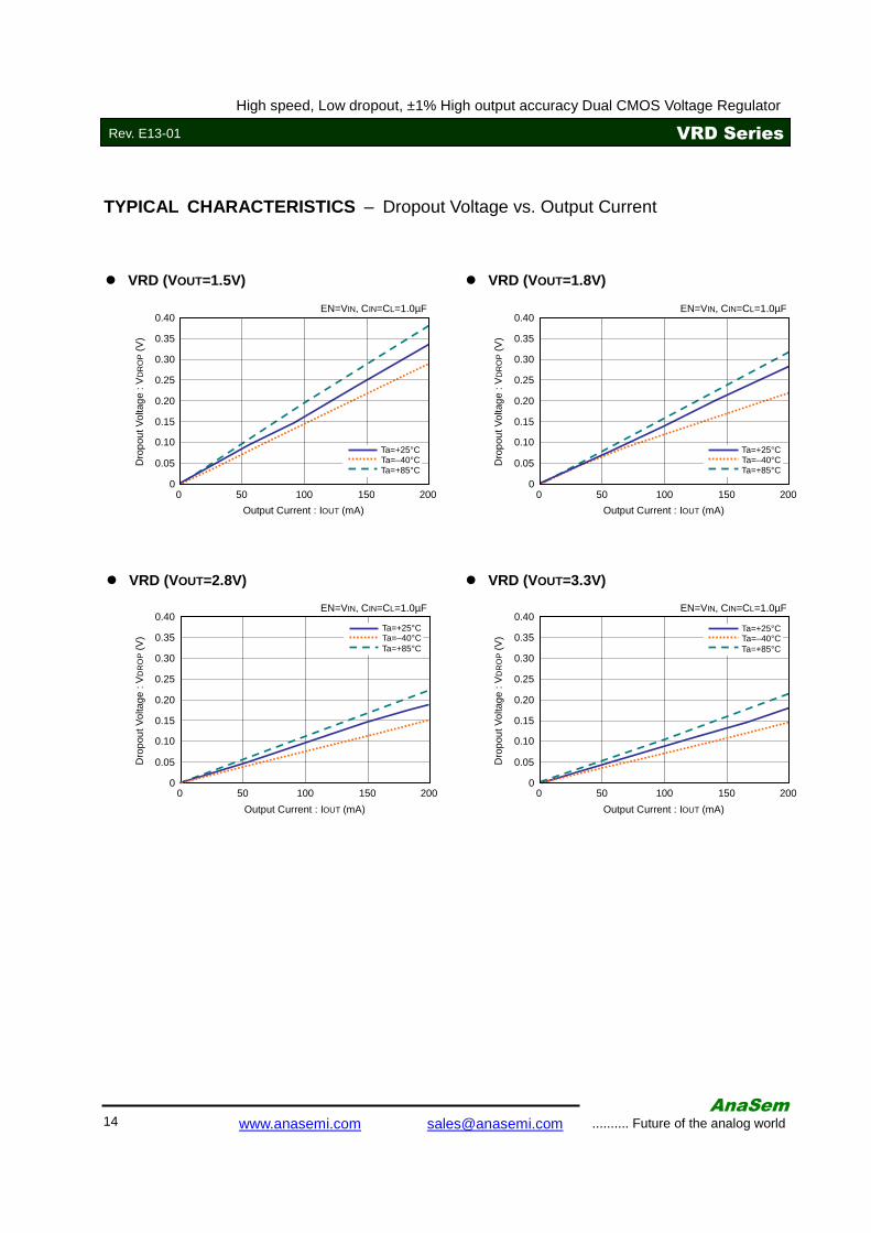
TYPICAL CHARACTERISTICS – Dropout Voltage vs. Output Current
Dro
pout
Vol
tage
: V
DR
OP (
V)
50 100 150 200 0
VRD (VOUT=1.5V)
Output Current : IOUT (mA)
EN=VIN, CIN=CL=1.0µF
50 100 150 200 0
VRD (VOUT=2.8V)
Output Current : IOUT (mA)
50 100 150 200 0
VRD (VOUT=3.3V)
Output Current : IOUT (mA)
50 100 150 200 0
VRD (VOUT=1.8V)
Output Current : IOUT (mA)
Ta=+25°C Ta=–40°C Ta=+85°C
Ta=+25°C Ta=–40°C Ta=+85°C
Ta=+25°C Ta=–40°C Ta=+85°C
Ta=+25°C Ta=–40°C Ta=+85°C
0.40
0.30
0.20
0
0.05
0.15
0.25
0.35
0.10
Dro
pout
Vol
tage
: V
DR
OP (
V)
0.40
0.30
0.20
0
0.05
0.15
0.25
0.35
0.10
Dro
pout
Vol
tage
: V
DR
OP (
V)
0.40
0.30
0.20
0
0.05
0.15
0.25
0.35
0.10
Dro
pout
Vol
tage
: V
DR
OP (
V)
0.40
0.30
0.20
0
0.05
0.15
0.25
0.35
0.10
EN=VIN, CIN=CL=1.0µF
EN=VIN, CIN=CL=1.0µF EN=VIN, CIN=CL=1.0µF
AnaSem
15 .......... Future of the analog world www.anasemi.com [email protected]
Rev. E13-01 VRD Series
High speed, Low dropout, ±1% High output accuracy Dual CMOS Voltage Regulator
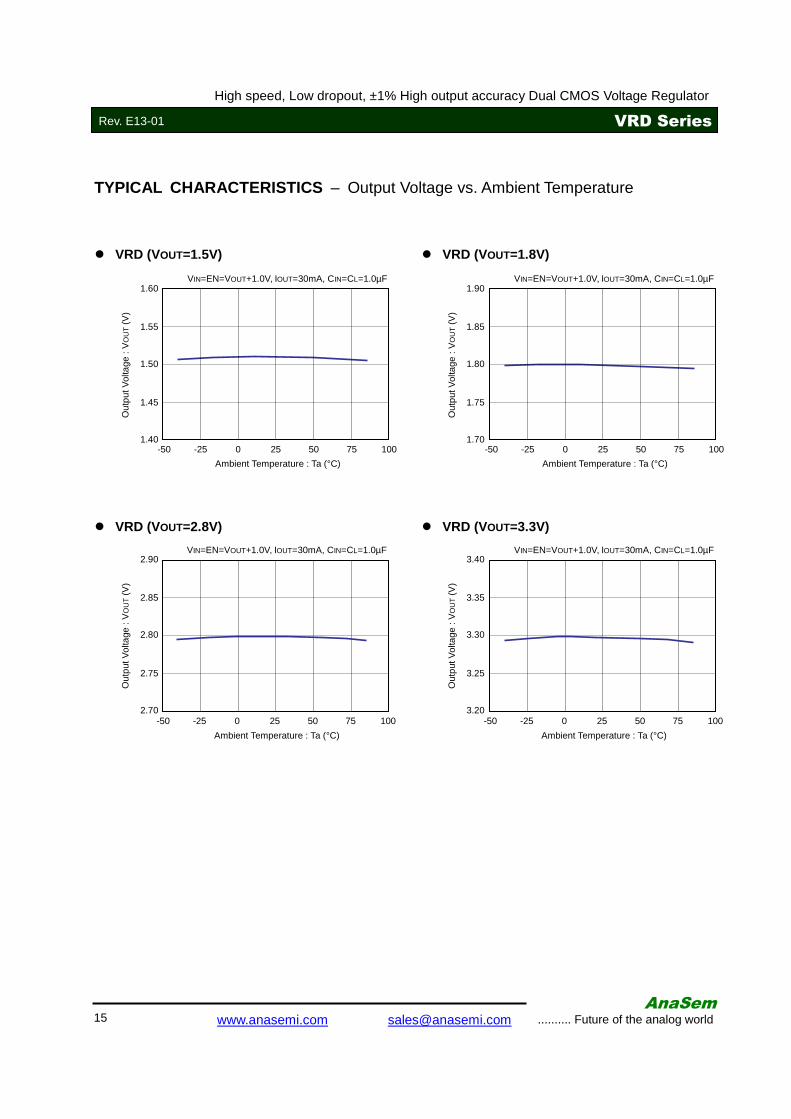
TYPICAL CHARACTERISTICS – Output Voltage vs. Ambient Temperature
Out
put V
olta
ge :
VO
UT (
V)
1.60
1.55
1.50
1.45
1.40 -25 25 50 75 100 -50
VRD (VOUT=1.5V)
Ambient Temperature : Ta (°C)
VIN=EN=VOUT+1.0V, IOUT=30mA, CIN=CL=1.0µF
0
-25 25 50 75 100 -50
VRD (VOUT=2.8V)
Ambient Temperature : Ta (°C)
VIN=EN=VOUT+1.0V, IOUT=30mA, CIN=CL=1.0µF
0 -25 25 50 75 100 -50
VRD (VOUT=3.3V)
Ambient Temperature : Ta (°C)
VIN=EN=VOUT+1.0V, IOUT=30mA, CIN=CL=1.0µF
0
-25 25 50 75 100 -50
VRD (VOUT=1.8V)
Ambient Temperature : Ta (°C)
VIN=EN=VOUT+1.0V, IOUT=30mA, CIN=CL=1.0µF
0 O
utpu
t Vol
tage
: V
OU
T (
V)
1.90
1.85
1.80
1.75
1.70
Out
put V
olta
ge :
VO
UT (
V)
2.90
2.85
2.80
2.75
2.70
Out
put V
olta
ge :
VO
UT (
V)
3.40
3.35
3.30
3.25
3.20
AnaSem
16 .......... Future of the analog world www.anasemi.com [email protected]
Rev. E13-01 VRD Series
High speed, Low dropout, ±1% High output accuracy Dual CMOS Voltage Regulator
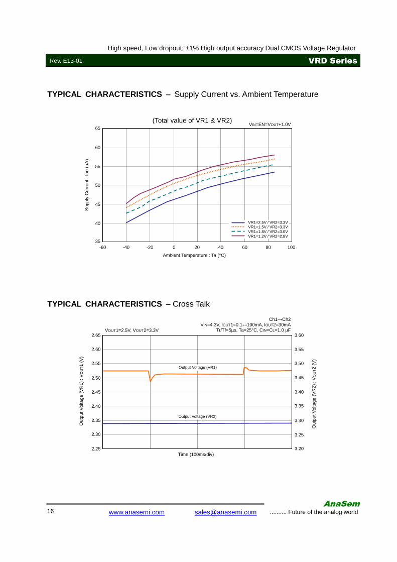
TYPICAL CHARACTERISTICS – Supply Current vs. Ambient Temperature
TYPICAL CHARACTERISTICS – Cross Talk
VIN=EN=VOUT+1.0V
Sup
ply
Cur
rent
: ID
D (
µA
)
65
60
45
35
50
-20 20 40 80 100 -60
Ambient Temperature : Ta (°C)
0 -40 60
55
40
VOUT1=2.5V, VOUT2=3.3V
Ch1→Ch2 VIN=4.3V, IOUT1=0.1↔100mA, IOUT2=30mA
Tr/Tf=5µs, Ta=25°C, CIN=CL=1.0 µF
Out
put V
olta
ge (
VR
2) :
VO
UT2
(V)
2.55
2.50
2.35
2.25
2.30
2.45
2.40
Time (100ms/div)
2.60
2.65
Output Voltage (VR1)
Output Voltage (VR2)
3.55
3.50
3.35
3.25
3.30
3.45
3.40
3.60
3.20
Out
put V
olta
ge (
VR
1) :
VO
UT1
(V)
VR1=2.5V / VR2=3.3V VR1=1.5V / VR2=3.3V VR1=1.8V / VR2=3.0V VR1=1.2V / VR2=2.8V
(Total value of VR1 & VR2)
AnaSem
17 .......... Future of the analog world www.anasemi.com [email protected]
Rev. E13-01 VRD Series
High speed, Low dropout, ±1% High output accuracy Dual CMOS Voltage Regulator
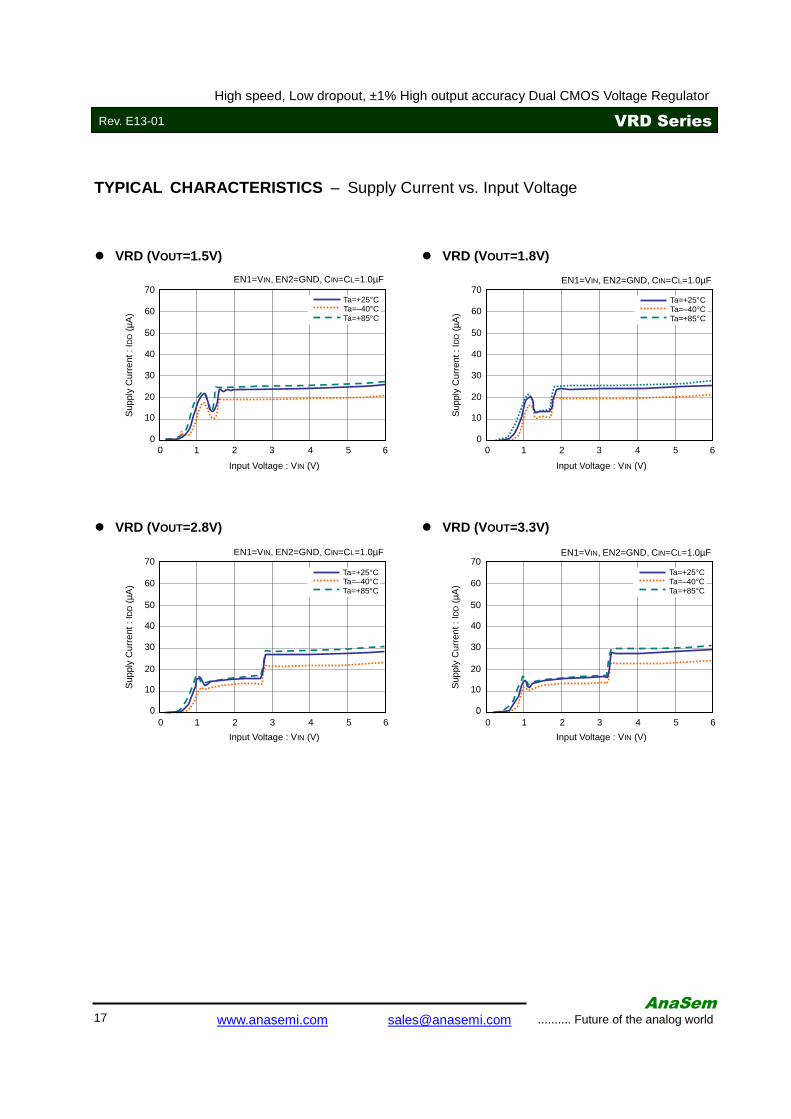
TYPICAL CHARACTERISTICS – Supply Current vs. Input Voltage
VRD (VOUT=1.5V)
EN1=VIN, EN2=GND, CIN=CL=1.0µF
Sup
ply
Cur
rent
: ID
D (
µA
)
1 2 4 5 6 0
Input Voltage : VIN (V)
3
VRD (VOUT=2.8V)
EN1=VIN, EN2=GND, CIN=CL=1.0µF
1 2 4 5 6 0
Input Voltage : VIN (V)
3
VRD (VOUT=3.3V)
EN1=VIN, EN2=GND, CIN=CL=1.0µF
1 2 4 5 6 0
Input Voltage : VIN (V)
3
60
50
20
0
10
40
70
30
VRD (VOUT=1.8V)
EN1=VIN, EN2=GND, CIN=CL=1.0µF
1 2 4 5 6 0
Input Voltage : VIN (V)
3
Ta=+25°C Ta=–40°C Ta=+85°C
Ta=+25°C Ta=–40°C Ta=+85°C
Ta=+25°C Ta=–40°C Ta=+85°C
Ta=+25°C Ta=–40°C Ta=+85°C
Sup
ply
Cur
rent
: ID
D (
µA
) 60
50
20
0
10
40
70
30
Sup
ply
Cur
rent
: ID
D (
µA
) 60
50
20
0
10
40
70
30
Sup
ply
Cur
rent
: ID
D (
µA
) 60
50
20
0
10
40
70
30
AnaSem
18 .......... Future of the analog world www.anasemi.com [email protected]
Rev. E13-01 VRD Series
High speed, Low dropout, ±1% High output accuracy Dual CMOS Voltage Regulator
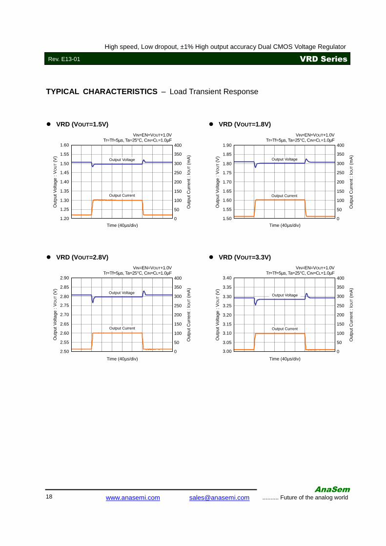
TYPICAL CHARACTERISTICS – Load Transient Response
VRD (VOUT=3.3V)
Time (40µs/div)
3.35
3.25
3.10
3.00
3.05
3.20
3.40
3.15
3.30
VRD (VOUT=1.5V)
VRD (VOUT=2.8V)
Time (40µs/div)
2.85
2.75
2.60
2.50
2.55
2.70
2.90
2.65
2.80
VRD (VOUT=1.8V)
Out
put V
olta
ge :
VO
UT (
V)
Time (40µs/div)
1.85
1.75
1.60
1.50
1.55
1.70
1.90
1.65
1.80
Out
put V
olta
ge :
VO
UT (
V)
Time (40µs/div)
Out
put C
urre
nt :
IOU
T (
mA
) 1.55
1.45
1.30
1.20
1.25
1.40
1.60
1.35
1.50
250
200
100
0
50
150
300
350
400
Out
put C
urre
nt :
IOU
T (
mA
)
250
200
100
0
50
150
300
350
400
Out
put V
olta
ge :
VO
UT (
V)
Out
put C
urre
nt :
I OU
T (
mA
)
250
200
100
0
50
150
300
350
400
Out
put V
olta
ge :
VO
UT (
V)
Out
put C
urre
nt :
IOU
T (
mA
)
250
200
100
0
50
150
300
350
400
Output Voltage
Output Current
Output Voltage
Output Current
Output Voltage
Output Current
Output Voltage
Output Current
VIN=EN=VOUT+1.0V Tr=Tf=5µs, Ta=25°C, CIN=CL=1.0µF
VIN=EN=VOUT+1.0V Tr=Tf=5µs, Ta=25°C, CIN=CL=1.0µF
VIN=EN=VOUT+1.0V Tr=Tf=5µs, Ta=25°C, CIN=CL=1.0µF
VIN=EN=VOUT+1.0V Tr=Tf=5µs, Ta=25°C, CIN=CL=1.0µF
AnaSem
19 .......... Future of the analog world www.anasemi.com [email protected]
Rev. E13-01 VRD Series
High speed, Low dropout, ±1% High output accuracy Dual CMOS Voltage Regulator
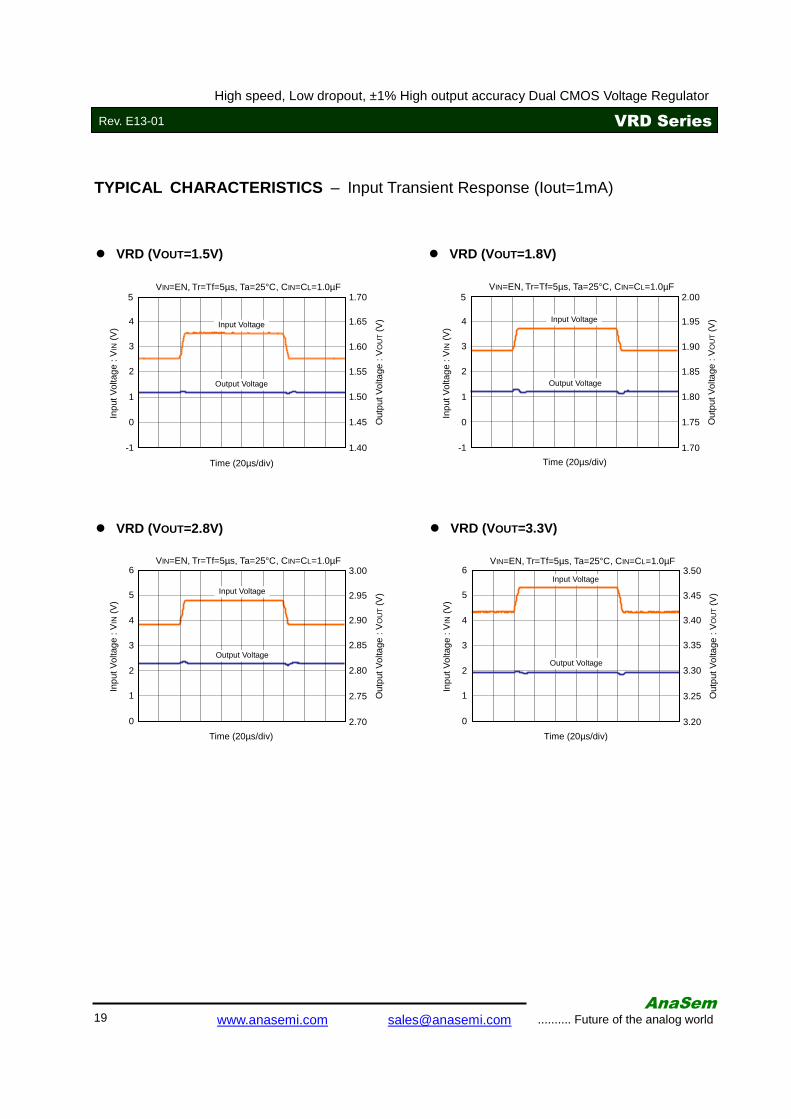
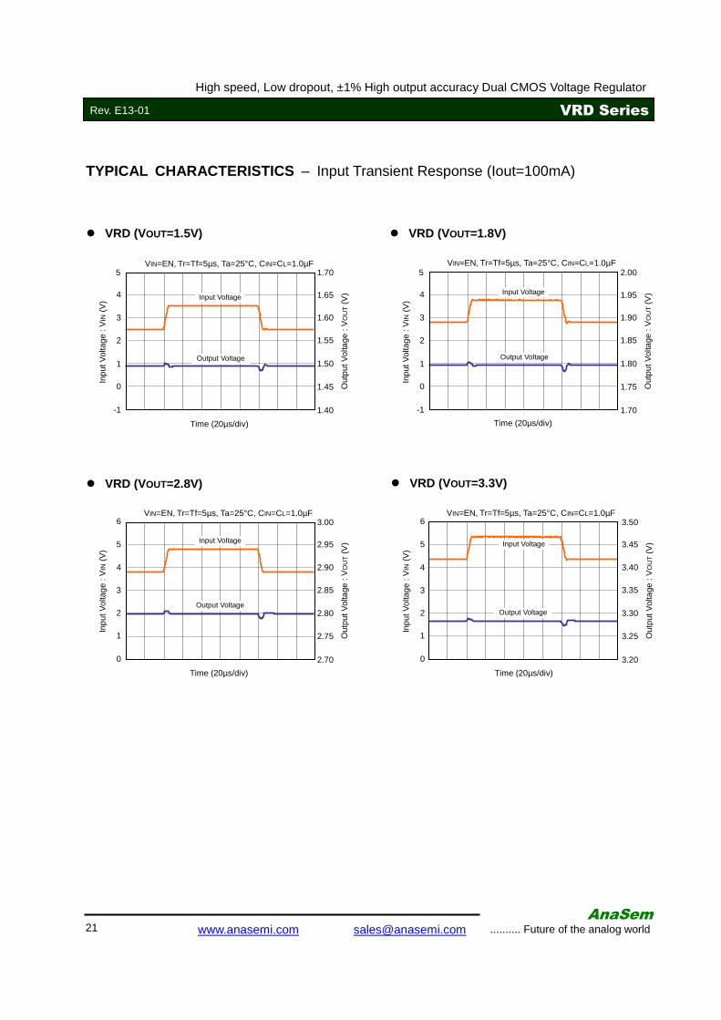
TYPICAL CHARACTERISTICS – Input Transient Response (Iout=1mA)
VRD (VOUT=1.5V)
VIN=EN, Tr=Tf=5µs, Ta=25°C, CIN=CL=1.0µF
Inpu
t Vol
tage
: V
IN (
V)
4
3
1
-1
0
2
5
Time (20µs/div)
1.65
1.60
1.50
1.40
1.45
1.55
1.70
Out
put V
olta
ge :
VO
UT (
V)
VRD (VOUT=1.8V)
VIN=EN, Tr=Tf=5µs, Ta=25°C, CIN=CL=1.0µF
Time (20µs/div)
VRD (VOUT=2.8V)
VIN=EN, Tr=Tf=5µs, Ta=25°C, CIN=CL=1.0µF
5
4
2
0
1
3
6
Time (20µs/div)
VRD (VOUT=3.3V)
VIN=EN, Tr=Tf=5µs, Ta=25°C, CIN=CL=1.0µF
Time (20µs/div)
Inpu
t Vol
tage
: V
IN (
V)
4
3
1
-1
0
2
5
1.95
1.90
1.80
1.70
1.75
1.85
2.00
Out
put V
olta
ge :
VO
UT (
V)
Inpu
t Vol
tage
: V
IN (
V)
2.95
2.90
2.80
2.70
2.75
2.85
3.00
Out
put V
olta
ge :
VO
UT (
V) 5
4
2
0
1
3
6
Inpu
t Vol
tage
: V
IN (
V)
3.45
3.40
3.30
3.20
3.25
3.35
3.50
Out
put V
olta
ge :
VO
UT (
V)
Input Voltage
Output Voltage
Input Voltage
Output Voltage
Input Voltage
Output Voltage
Input Voltage
Output Voltage

AnaSem
20 .......... Future of the analog world www.anasemi.com [email protected]
Rev. E13-01 VRD Series
High speed, Low dropout, ±1% High output accuracy Dual CMOS Voltage Regulator
TYPICAL CHARACTERISTICS – Input Transient Response (Iout=30mA)
VRD (VOUT=1.5V)
VIN=EN, Tr=Tf=5µs, Ta=25°C, CIN=CL=1.0µF
Inpu
t Vol
tage
: V
IN (
V)
4
3
1
-1
0
2
5
Time (20µs/div)
1.65
1.60
1.50
1.40
1.45
1.55
1.70
Out
put V
olta
ge :
VO
UT (
V)
VRD (VOUT=1.8V)
VIN=EN, Tr=Tf=5µs, Ta=25°C, CIN=CL=1.0µF
Time (20µs/div)
VRD (VOUT=2.8V)
VIN=EN, Tr=Tf=5µs, Ta=25°C, CIN=CL=1.0µF
5
4
2
0
1
3
6
Time (20µs/div)
VRD (VOUT=3.3V)
VIN=EN, Tr=Tf=5µs, Ta=25°C, CIN=CL=1.0µF
Time (20µs/div)
Inpu
t Vol
tage
: V
IN (
V)
4
3
1
-1
0
2
5
1.95
1.90
1.80
1.70
1.85
2.00
Out
put V
olta
ge :
VO
UT (
V)
Inpu
t Vol
tage
: V
IN (
V)
2.95
2.90
2.80
2.70
2.75
2.85
3.00
Out
put V
olta
ge :
VO
UT (
V) 5
4
2
0
1
3
6
Inpu
t Vol
tage
: V
IN (
V)
3.45
3.40
3.30
3.20
3.25
3.35
3.50
Out
put V
olta
ge :
VO
UT (
V) Input Voltage
Output Voltage
Input Voltage
Output Voltage
Input Voltage
Output Voltage
Input Voltage
Output Voltage
1.75
AnaSem
21 .......... Future of the analog world www.anasemi.com [email protected]
Rev. E13-01 VRD Series
High speed, Low dropout, ±1% High output accuracy Dual CMOS Voltage Regulator
TYPICAL CHARACTERISTICS – Input Transient Response (Iout=100mA)
VRD (VOUT=1.5V)
VIN=EN, Tr=Tf=5µs, Ta=25°C, CIN=CL=1.0µF
Inpu
t Vol
tage
: V
IN (
V)
4
3
1
-1
0
2
5
Time (20µs/div)
1.65
1.60
1.50
1.40
1.45
1.55
1.70
Out
put V
olta
ge :
VO
UT (
V)
VRD (VOUT=1.8V)
VIN=EN, Tr=Tf=5µs, Ta=25°C, CIN=CL=1.0µF
Time (20µs/div)
VRD (VOUT=2.8V)
VIN=EN, Tr=Tf=5µs, Ta=25°C, CIN=CL=1.0µF
5
4
2
0
1
3
6
Time (20µs/div)
VRD (VOUT=3.3V)
VIN=EN, Tr=Tf=5µs, Ta=25°C, CIN=CL=1.0µF
Time (20µs/div)
Inpu
t Vol
tage
: V
IN (
V)
4
3
1
-1
0
2
5
1.95
1.90
1.80
1.70
1.75
1.85
2.00
Out
put V
olta
ge :
VO
UT (
V)
Inpu
t Vol
tage
: V
IN (
V)
2.95
2.90
2.80
2.70
2.75
2.85
3.00
Out
put V
olta
ge :
VO
UT (
V) 5
4
2
0
1
3
6
Inpu
t Vol
tage
: V
IN (
V)
3.45
3.40
3.30
3.20
3.25
3.35
3.50
Out
put V
olta
ge :
VO
UT (
V) Input Voltage
Output Voltage
Input Voltage
Output Voltage
Input Voltage
Output Voltage
Input Voltage
Output Voltage
AnaSem
22 .......... Future of the analog world www.anasemi.com [email protected]
Rev. E13-01 VRD Series
High speed, Low dropout, ±1% High output accuracy Dual CMOS Voltage Regulator
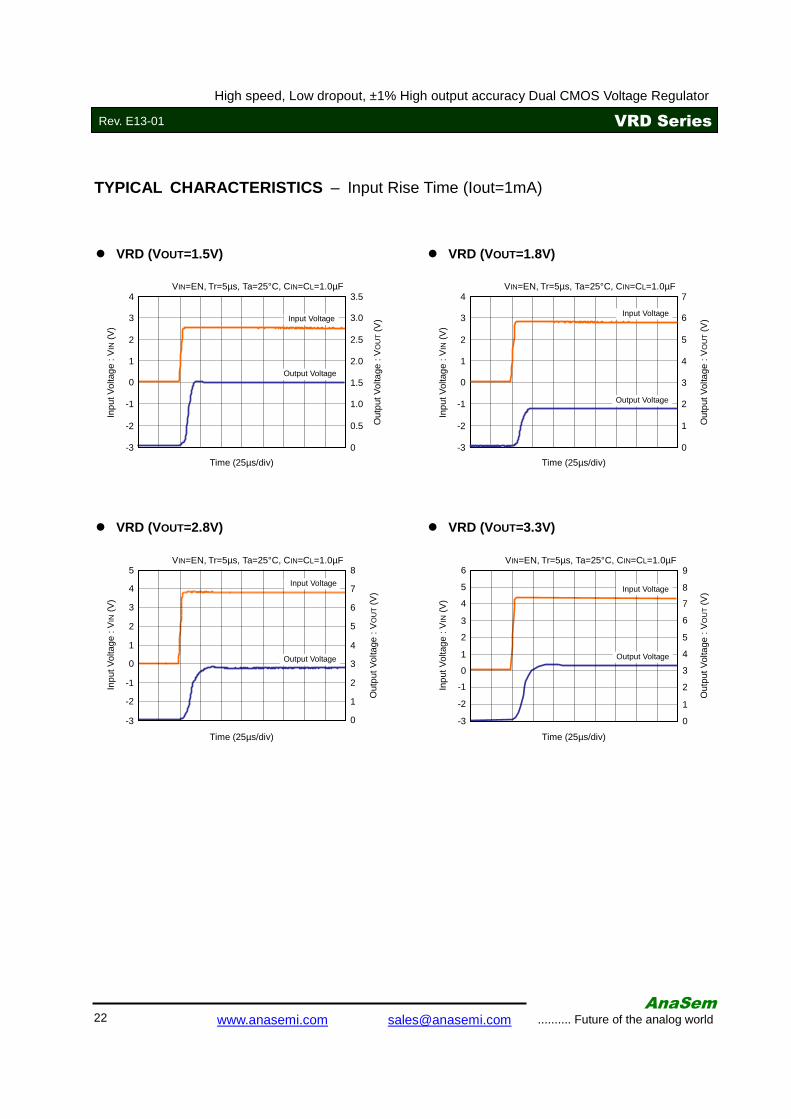
TYPICAL CHARACTERISTICS – Input Rise Time (Iout=1mA)
VRD (VOUT=1.5V)
VIN=EN, Tr=5µs, Ta=25°C, CIN=CL=1.0µF
Inpu
t Vol
tage
: V
IN (
V)
Out
put V
olta
ge :
VO
UT (
V)
4
3
-1
-3
-2
2
1
0
3.5
3.0
1.0
0
0.5
2.5
2.0
1.5
Time (25µs/div)
VRD (VOUT=1.8V)
Time (25µs/div)
VRD (VOUT=2.8V)
Out
put V
olta
ge :
VO
UT (
V)
Time (25µs/div)
VRD (VOUT=3.3V)
Time (25µs/div)
5
3
-1
-3
-2
2
1
0
4
8
6
2
0
1
5
4
3
7
6
3
-1
-3
-2
2
1
0
4
5
6
2
0
1
5
4
3
7
8
9
Inpu
t Vol
tage
: V
IN (
V)
4
3
-1
-3
-2
2
1
0
Out
put V
olta
ge :
VO
UT (
V)
7
6
2
0
1
5
4
3
Inpu
t Vol
tage
: V
IN (
V)
Inpu
t Vol
tage
: V
IN (
V)
Out
put V
olta
ge :
VO
UT (
V)
Input Voltage
Output Voltage
Input Voltage
Output Voltage
Input Voltage
Output Voltage
Input Voltage
Output Voltage
VIN=EN, Tr=5µs, Ta=25°C, CIN=CL=1.0µF
VIN=EN, Tr=5µs, Ta=25°C, CIN=CL=1.0µF VIN=EN, Tr=5µs, Ta=25°C, CIN=CL=1.0µF
AnaSem
23 .......... Future of the analog world www.anasemi.com [email protected]
Rev. E13-01 VRD Series
High speed, Low dropout, ±1% High output accuracy Dual CMOS Voltage Regulator
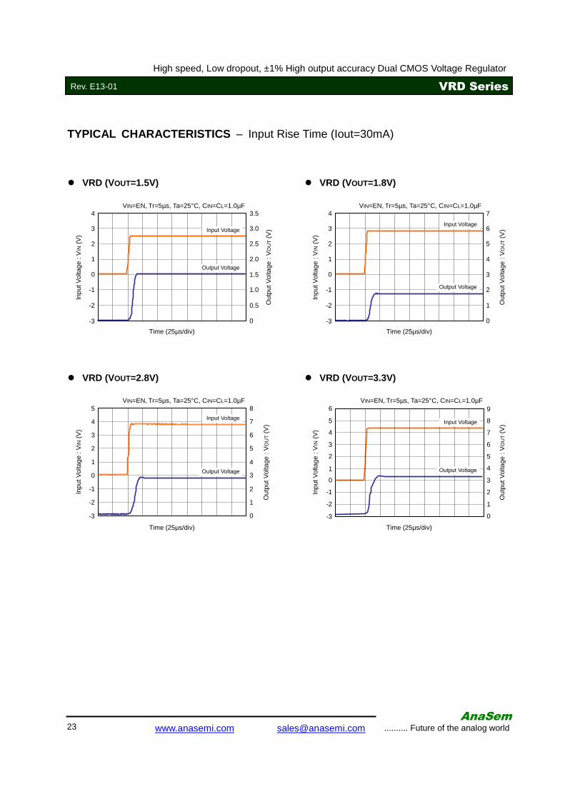
TYPICAL CHARACTERISTICS – Input Rise Time (Iout=30mA)
VRD (VOUT=1.5V)
Inpu
t Vol
tage
: V
IN (
V)
Out
put V
olta
ge :
VO
UT (
V)
4
3
-1
-3
-2
2
1
0
3.5
3.0
1.0
0
0.5
2.5
2.0
1.5
Time (25µs/div)
VRD (VOUT=1.8V)
Time (25µs/div)
VRD (VOUT=2.8V)
Out
put V
olta
ge :
VO
UT (
V)
Time (25µs/div)
VRD (VOUT=3.3V)
Time (25µs/div)
5
3
-1
-3
-2
2
1
0
4
8
6
2
0
1
5
4
3
7
6
3
-1
-3
-2
2
1
0
4
5
6
2
0
1
5
4
3
7
8
9
Inpu
t Vol
tage
: V
IN (
V)
4
3
-1
-3
-2
2
1
0
Out
put V
olta
ge :
VO
UT (
V)
7
6
2
0
1
5
4
3
Inpu
t Vol
tage
: V
IN (
V)
Inpu
t Vol
tage
: V
IN (
V)
Out
put V
olta
ge :
VO
UT (
V)
Input Voltage
Output Voltage
Input Voltage
Output Voltage
Input Voltage
Output Voltage
Input Voltage
Output Voltage
VIN=EN, Tr=5µs, Ta=25°C, CIN=CL=1.0µF VIN=EN, Tr=5µs, Ta=25°C, CIN=CL=1.0µF
VIN=EN, Tr=5µs, Ta=25°C, CIN=CL=1.0µF VIN=EN, Tr=5µs, Ta=25°C, CIN=CL=1.0µF
AnaSem
24 .......... Future of the analog world www.anasemi.com [email protected]
Rev. E13-01 VRD Series
High speed, Low dropout, ±1% High output accuracy Dual CMOS Voltage Regulator
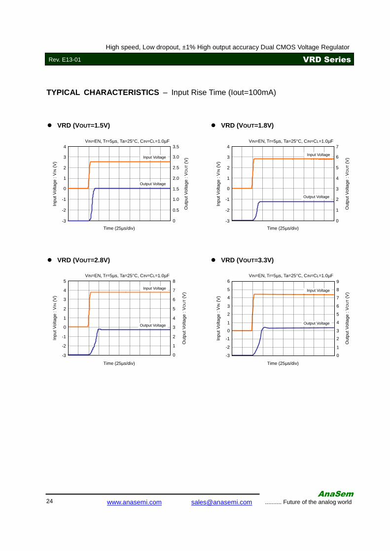
TYPICAL CHARACTERISTICS – Input Rise Time (Iout=100mA)
VRD (VOUT=1.5V)
Inpu
t Vol
tage
: V
IN (
V)
Out
put V
olta
ge :
VO
UT (
V)
4
3
-1
-3
-2
2
1
0
3.5
3.0
1.0
0
0.5
2.5
2.0
1.5
Time (25µs/div)
VRD (VOUT=1.8V)
Time (25µs/div)
VRD (VOUT=2.8V)
Out
put V
olta
ge :
VO
UT (
V)
Time (25µs/div)
VRD (VOUT=3.3V)
Time (25µs/div)
5
3
-1
-3
-2
2
1
0
4
8
6
2
0
1
5
4
3
7
6
3
-1
-3
-2
2
1
0
4
5
6
2
0
1
5
4
3
7
8
9
Inpu
t Vol
tage
: V
IN (
V)
4
3
-1
-3
-2
2
1
0
Out
put V
olta
ge :
VO
UT (
V)
7
6
2
0
1
5
4
3
Inpu
t Vol
tage
: V
IN (
V)
Inpu
t Vol
tage
: V
IN (
V)
Out
put V
olta
ge :
VO
UT (
V)
Input Voltage
Output Voltage
Input Voltage
Output Voltage
Input Voltage
Output Voltage
Input Voltage
Output Voltage
VIN=EN, Tr=5µs, Ta=25°C, CIN=CL=1.0µF VIN=EN, Tr=5µs, Ta=25°C, CIN=CL=1.0µF
VIN=EN, Tr=5µs, Ta=25°C, CIN=CL=1.0µF VIN=EN, Tr=5µs, Ta=25°C, CIN=CL=1.0µF
AnaSem
25 .......... Future of the analog world www.anasemi.com [email protected]
Rev. E13-01 VRD Series
High speed, Low dropout, ±1% High output accuracy Dual CMOS Voltage Regulator
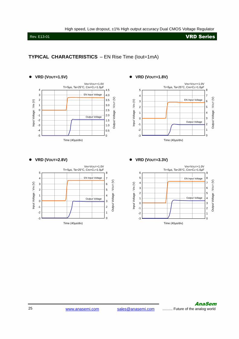
TYPICAL CHARACTERISTICS – EN Rise Time (Iout=1mA)
VRD (VOUT=1.5V)
Inpu
t Vol
tage
: V
IN (
V)
Out
put V
olta
ge :
VO
UT (
V)
Time (40µs/div)
VRD (VOUT=1.8V)
Time (40µs/div)
VRD (VOUT=2.8V)
Out
put V
olta
ge :
VO
UT (
V)
Time (40µs/div)
VRD (VOUT=3.3V)
Time (40µs/div)
5
3
-1
-3
-2
2
1
0
4
8
6
2
0
1
5
4
3
7
6
3
-1
-3
-2
2
1
0
4
5
6
2
0
1
5
4
3
7
8
9
Inpu
t Vol
tage
: V
IN (
V)
Inpu
t Vol
tage
: V
IN (
V)
Out
put V
olta
ge :
VO
UT (
V)
EN Input Voltage
Output Voltage
EN Input Voltage
Output Voltage
Output Voltage Output Voltage
5
3
-1
-3
-2
2
1
0
4
Inpu
t Vol
tage
: V
IN (
V)
Out
put V
olta
ge :
VO
UT (
V)
8
6
2
0
1
5
4
3
7
4
1
-3
-5
-4
0
-1
-2
2
3
3.0
1.0
0
0.5
2.5
2.0
1.5
3.5
4.0
4.5
EN Input Voltage EN Input Voltage
VIN=VOUT+1.0V Tr=5µs, Ta=25°C, CIN=CL=1.0µF
VIN=VOUT+1.0V Tr=5µs, Ta=25°C, CIN=CL=1.0µF
VIN=VOUT+1.0V Tr=5µs, Ta=25°C, CIN=CL=1.0µF
VIN=VOUT+1.0V Tr=5µs, Ta=25°C, CIN=CL=1.0µF
AnaSem
26 .......... Future of the analog world www.anasemi.com [email protected]
Rev. E13-01 VRD Series
High speed, Low dropout, ±1% High output accuracy Dual CMOS Voltage Regulator
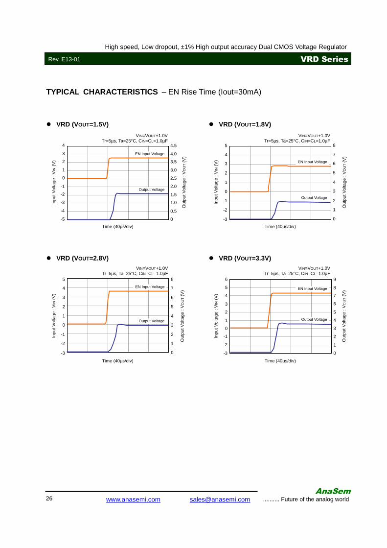
TYPICAL CHARACTERISTICS – EN Rise Time (Iout=30mA)
VRD (VOUT=1.5V)
VIN=VOUT+1.0V Tr=5µs, Ta=25°C, CIN=CL=1.0µF
Inpu
t Vol
tage
: V
IN (
V)
Out
put V
olta
ge :
VO
UT (
V)
Time (40µs/div)
VRD (VOUT=1.8V)
Time (40µs/div)
VRD (VOUT=2.8V)
Out
put V
olta
ge :
VO
UT (
V)
Time (40µs/div)
VRD (VOUT=3.3V)
Time (40µs/div)
5
3
-1
-3
-2
2
1
0
4
8
6
2
0
1
5
4
3
7
6
3
-1
-3
-2
2
1
0
4
5
6
2
0
1
5
4
3
7
8
9
Inpu
t Vol
tage
: V
IN (
V)
Inpu
t Vol
tage
: V
IN (
V)
Out
put V
olta
ge :
VO
UT (
V)
EN Input Voltage
Output Voltage
EN Input Voltage
Output Voltage
Output Voltage Output Voltage
5
3
-1
-3
-2
2
1
0
4
Inpu
t Vol
tage
: V
IN (
V)
Out
put V
olta
ge :
VO
UT (
V)
8
6
2
0
1
5
4
3
7
4
1
-3
-5
-4
0
-1
-2
2
3
3.0
1.0
0
0.5
2.5
2.0
1.5
3.5
4.0
4.5
EN Input Voltage EN Input Voltage
VIN=VOUT+1.0V Tr=5µs, Ta=25°C, CIN=CL=1.0µF
VIN=VOUT+1.0V Tr=5µs, Ta=25°C, CIN=CL=1.0µF
VIN=VOUT+1.0V Tr=5µs, Ta=25°C, CIN=CL=1.0µF
AnaSem
27 .......... Future of the analog world www.anasemi.com [email protected]
Rev. E13-01 VRD Series
High speed, Low dropout, ±1% High output accuracy Dual CMOS Voltage Regulator
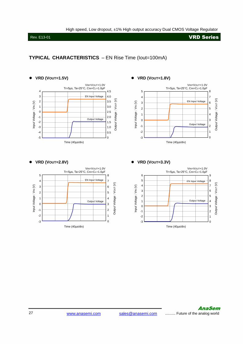
TYPICAL CHARACTERISTICS – EN Rise Time (Iout=100mA)
VRD (VOUT=1.5V)
Inpu
t Vol
tage
: V
IN (
V)
Out
put V
olta
ge :
VO
UT (
V)
Time (40µs/div)
VRD (VOUT=1.8V)
Time (40µs/div)
VRD (VOUT=2.8V)
Out
put V
olta
ge :
VO
UT (
V)
Time (40µs/div)
VRD (VOUT=3.3V)
Time (40µs/div)
5
3
-1
-3
-2
2
1
0
4
8
6
2
0
1
5
4
3
7
6
3
-1
-3
-2
2
1
0
4
5
6
2
0
1
5
4
3
7
8
9
Inpu
t Vol
tage
: V
IN (
V)
Inpu
t Vol
tage
: V
IN (
V)
Out
put V
olta
ge :
VO
UT (
V)
EN Input Voltage
Output Voltage
EN Input Voltage
Output Voltage
Output Voltage Output Voltage
5
3
-1
-3
-2
2
1
0
4
Inpu
t Vol
tage
: V
IN (
V)
Out
put V
olta
ge :
VO
UT (
V)
8
6
2
0
1
5
4
3
7
4
1
-3
-5
-4
0
-1
-2
2
3
3.0
1.0
0
0.5
2.5
2.0
1.5
3.5
4.0
4.5
EN Input Voltage EN Input Voltage
VIN=VOUT+1.0V Tr=5µs, Ta=25°C, CIN=CL=1.0µF
VIN=VOUT+1.0V Tr=5µs, Ta=25°C, CIN=CL=1.0µF
VIN=VOUT+1.0V Tr=5µs, Ta=25°C, CIN=CL=1.0µF
VIN=VOUT+1.0V Tr=5µs, Ta=25°C, CIN=CL=1.0µF
AnaSem
28 .......... Future of the analog world www.anasemi.com [email protected]
Rev. E13-01 VRD Series
High speed, Low dropout, ±1% High output accuracy Dual CMOS Voltage Regulator
TYPICAL CHARACTERISTICS – Ripple Rejection Rate
VRD (VOUT=1.5V)
Rip
ple
Rej
ectio
n R
ate
: RR
(dB
)
0.01
Ripple Frequency : f (KHz)
VIN=EN=(VOUT+1.0)Vdc+0.5Vp-pac IOUT=30mA, Ta=25°C, CIN=CL=1.0µF
0.1 1 10 100 1000
VRD (VOUT=1.8V)
Rip
ple
Rej
ectio
n R
ate
: RR
(dB
)
0.01
Ripple Frequency : f (KHz)
VIN=EN=(VOUT+1.0)Vdc +0.5Vp-pac IOUT=30mA, Ta=25°C, CIN=CL=1.0µF
0.1 1 10 100 1000
VRD (VOUT=2.8V)
Rip
ple
Rej
ectio
n R
ate
: RR
(dB
)
0.01
Ripple Frequency : f (KHz)
VIN=EN=(VOUT+1.0)Vdc +0.5Vp-pac IOUT=30mA, Ta=25°C, CIN=CL=1.0µF
0.1 1 10 100 1000
120
110
100
90
80
70
60
50
40
30
20
10
0
120
110
100
90
80
70
60
50
40
30
20
10
0
120
110
100
90
80
70
60
50
40
30
20
10
0
VRD (VOUT=3.3V)
Rip
ple
Rej
ectio
n R
ate
: RR
(dB
)
0.01
Ripple Frequency : f (KHz)
VIN=EN=(VOUT+1.0)Vdc +0.5Vp-pac IOUT=30mA, Ta=25°C, CIN=CL=1.0µF
0.1 1 10 100 1000
120
110
100
90
80
70
60
50
40
30
20
10
0
AnaSem
29 .......... Future of the analog world www.anasemi.com [email protected]
Rev. E13-01 VRD Series
High speed, Low dropout, ±1% High output accuracy Dual CMOS Voltage Regulator
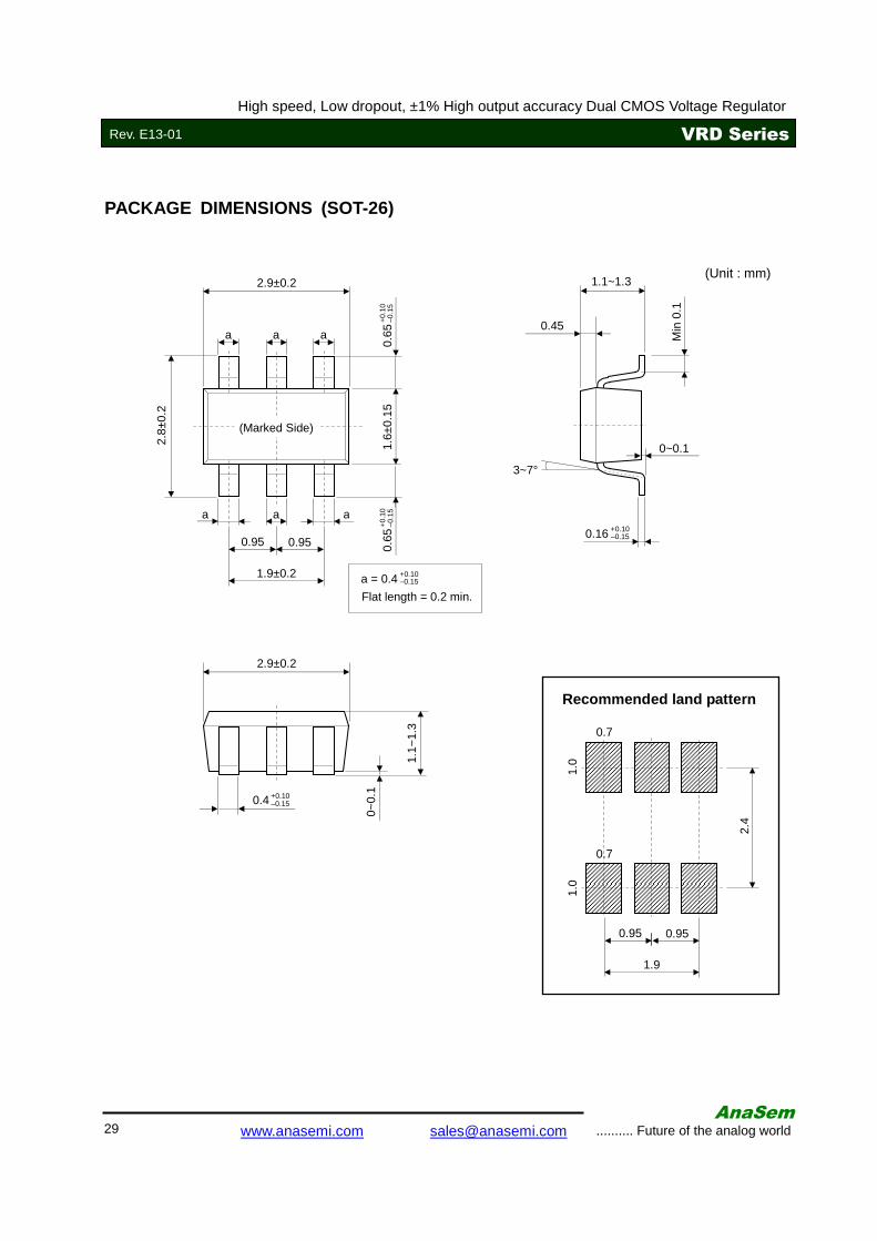
PACKAGE DIMENSIONS (SOT-26)
Recommended land pattern
2.4
1.0
0.7
1.9
0.95 0.95
1.0
0.7
2.9±0.2
1.9±0.2
0.95 0.95
a
0.65
+0.
10
–0.1
5 0.
65 +
0.10
–0
.15
(Marked Side)
a = 0.4 +0.10 –0.15
a
a a a
Flat length = 0.2 min.
a
1.6±
0.15
2.8±
0.2
(Unit : mm)
1.1~
1.3
0~0.
1
2.9±0.2
0.4 +0.10 –0.15
3~7°
0.16 +0.10 –0.15
Min
0.1
0~0.1
1.1~1.3
0.45
AnaSem
30 .......... Future of the analog world www.anasemi.com [email protected]
Rev. E13-01 VRD Series
High speed, Low dropout, ±1% High output accuracy Dual CMOS Voltage Regulator
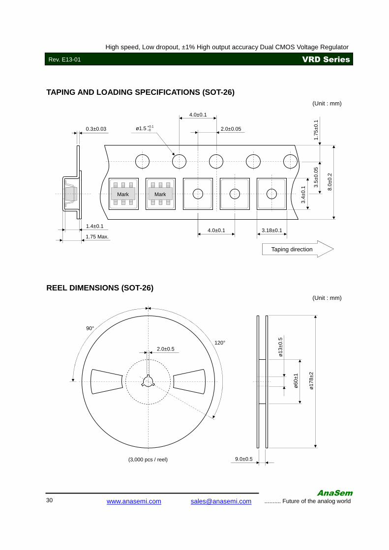
TAPING AND LOADING SPECIFICATIONS (SOT-26)
REEL DIMENSIONS (SOT-26)
(Unit : mm)
ø13
±0.5
ø
60±1
ø
178±
2
90°
120°
2.0±0.5
9.0±0.5 (3,000 pcs / reel)
(Unit : mm)
Taping direction
4.0±0.1
2.0±0.05
4.0±0.1
ø1.5 +0.1 –0
3.18±0.1
3.4±
0.1 3.
5±0.
05
1.75
±0.1
8.0±
0.2
1.75 Max.
0.3±0.03
Taping direction
1.4±0.1
Mark Mark
AnaSem
31 .......... Future of the analog world www.anasemi.com [email protected]
Rev. E13-01 VRD Series
High speed, Low dropout, ±1% High output accuracy Dual CMOS Voltage Regulator
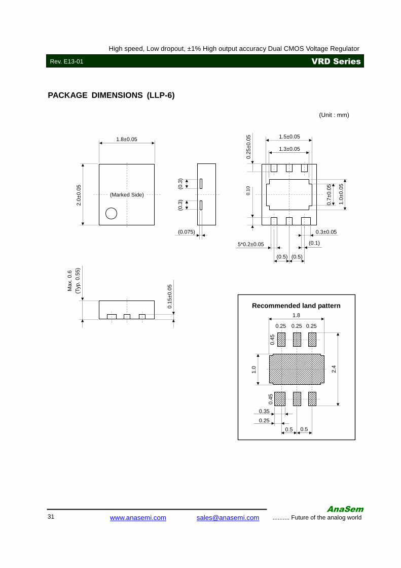
PACKAGE DIMENSIONS (LLP-6)
(Unit : mm)
1.8±0.05
2.0±
0.05
(Marked Side)
1.5±0.05
0.7±
0.05
5*0.2±0.05
0.3±0.05
0.25
±0.0
5
Max
. 0.6
(Typ
. 0.5
5)
(0.1)
Recommended land pattern
2.4
0.45
0.25
0.5 0.5
0.25 0.25
0.45
0.35
1.0
1.8
0.25
0.15
±0.0
5
(0.5) (0.5)
1.3±0.05
1.0±
0.05
(0.3
) (0
.3)
(0.075)
0.10
AnaSem
32 .......... Future of the analog world www.anasemi.com [email protected]
Rev. E13-01 VRD Series
High speed, Low dropout, ±1% High output accuracy Dual CMOS Voltage Regulator
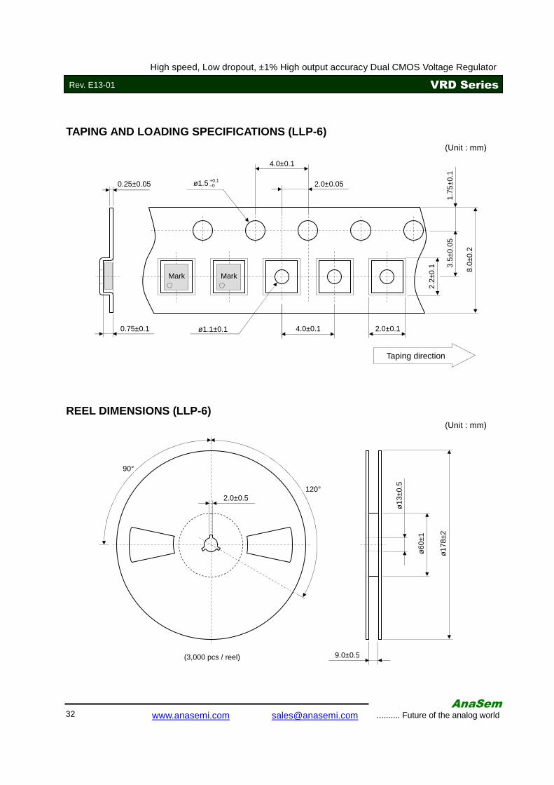
TAPING AND LOADING SPECIFICATIONS (LLP-6)
REEL DIMENSIONS (LLP-6)
(Unit : mm)
ø13
±0.5
ø
60±1
ø
178±
2
90°
120°
2.0±0.5
9.0±0.5 (3,000 pcs / reel)
(Unit : mm)
4.0±0.1
2.0±0.05
4.0±0.1
ø1.5 +0.1 –0
ø1.1±0.1 2.0±0.1
2.2±
0.1 3.
5±0.
05
1.75
±0.1
8.0±
0.2
0.75±0.1
0.25±0.05
Taping direction
Mark Mark
AnaSem
AnaSem
AnaSem may change the products described in this data sheet, or may discontinue production or services without any notice in order to supply the best products through improve the design and performance. Customers are recommended to obtain the latest data or information before placing orders in order to make sure the data or information required is the newest. It is necessary for customers to fully understand the products described in this data sheet and to use it in accordance with its specifications. The products described in this data sheet are not intended to use for the apparatus which have influence on human lives due to the failure or malfunction of the products. AnaSem Corp. is not responsible for any support to customer’s application, product design, software performance, patent infringement or service. AnaSem Corp. does not disclose or imply a guarantee or description about being licensed based on patents, copy-rights, circuit location license, or other intellectual properties associated with the devices or combinations in which the products or service of AnaSem Corp. are used or can be used, or which cover the methods. Customers should not export, directly or indirectly, any products without obtaining required licenses and approvals in advance from appropriate government agencies.
www.anasemi.com [email protected]
AnaSem
2 .......... Future of the analog world
www.anasemi.com [email protected]
Rev. E13-01 VRD Series
High speed, Low dropout, ±1% High output accuracy Dual CMOS Voltage Regulator
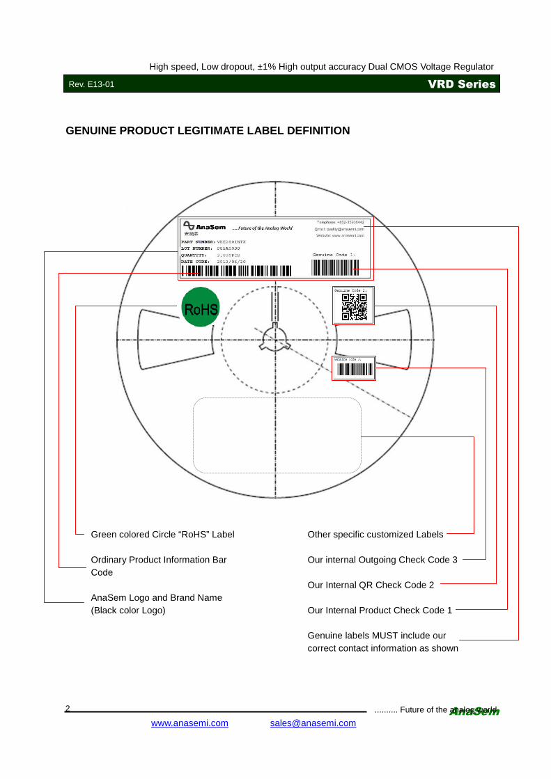
GENUINE PRODUCT LEGITIMATE LABEL DEFINITION
Green colored Circle “RoHS” Label Other specific customized Labels Ordinary Product Information Bar Our internal Outgoing Check Code 3 Code Our Internal QR Check Code 2 AnaSem Logo and Brand Name (Black color Logo) Our Internal Product Check Code 1 Genuine labels MUST include our
correct contact information as shown