Embed Size (px)
Citation preview

Company Logo
December 8 2015
1
Annual Meeting
Arizona State University Raja Ayyanar
January 17-19-2017
Company Logo
2
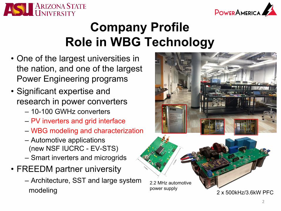
Company Profile Role in WBG Technology
• One of the largest universities in the nation, and one of the largest Power Engineering programs
• Significant expertise and research in power converters
– 10-100 GWHz converters – PV inverters and grid interface – WBG modeling and characterization – Automotive applications (new NSF IUCRC - EV-STS)
– Smart inverters and microgrids
• FREEDM partner university – Architecture, SST and large system modeling
2 x 500kHz/3.6kW PFC
2.2 MHz automotive power supply
Company Logo
3
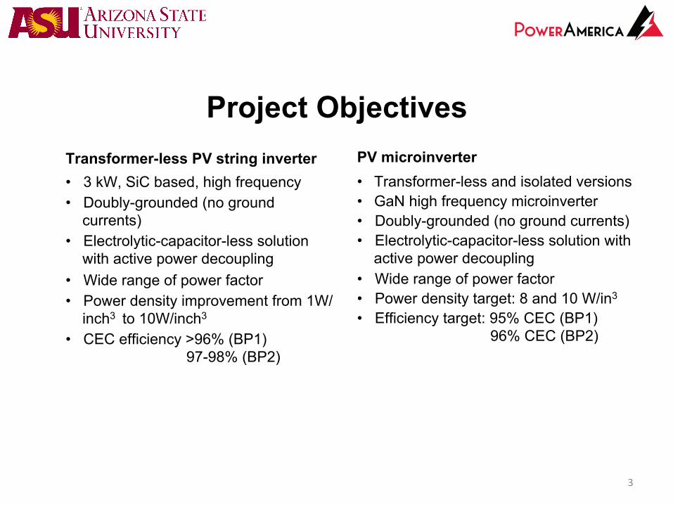
Project Objectives Transformer-less PV string inverter • 3 kW, SiC based, high frequency • Doubly-grounded (no ground
currents) • Electrolytic-capacitor-less solution
with active power decoupling • Wide range of power factor • Power density improvement from 1W/
inch3 to 10W/inch3 • CEC efficiency >96% (BP1)
97-98% (BP2)
PV microinverter • Transformer-less and isolated versions • GaN high frequency microinverter • Doubly-grounded (no ground currents) • Electrolytic-capacitor-less solution with
active power decoupling • Wide range of power factor • Power density target: 8 and 10 W/in3 • Efficiency target: 95% CEC (BP1)
96% CEC (BP2)

Company Logo
Accomplishments and Outcomes
4
Company Logo
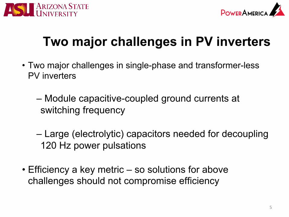
Two major challenges in PV inverters
5
• Two major challenges in single-phase and transformer-less PV inverters
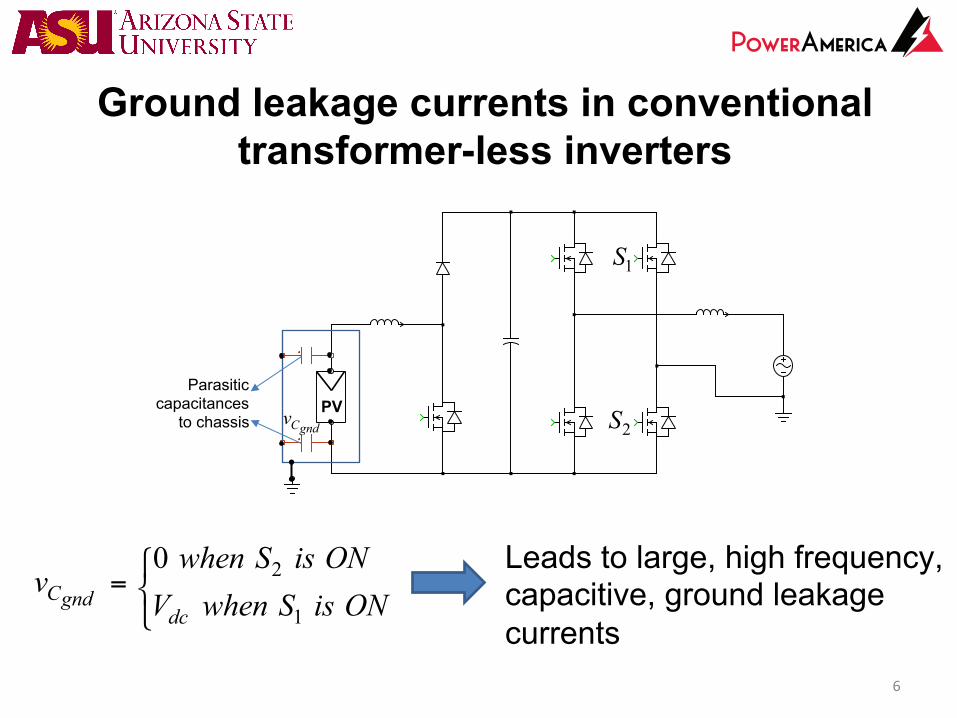
– Module capacitive-coupled ground currents at switching frequency
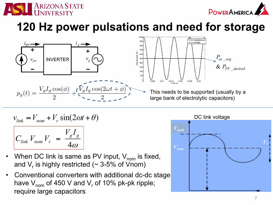
– Large (electrolytic) capacitors needed for decoupling 120 Hz power pulsations
• Efficiency a key metric – so solutions for above challenges should not compromise efficiency
Company Logo
Ground leakage currents in conventional transformer-less inverters
6
2
1
0Cgnd
dc
when S is ONv
V when S is ON⎧
= ⎨⎩
1S
2S
Leads to large, high frequency, capacitive, ground leakage currents
PV Cgndv
Parasitic capacitances
to chassis
Company Logo
120 Hz power pulsations and need for storage
7
_
_&ac avg
PV desired
P
P
This needs to be supported (usually by a large bank of electrolytic capacitors)
DC link voltage
Vpeak
Vnom Vr
sin(2 )link nom rv V V tω θ≈ + +
4g g
link nom r
V IC V V
ω=
• When DC link is same as PV input, Vnom is fixed, and Vr is highly restricted (~ 3-5% of Vnom)
• Conventional converters with additional dc-dc stage have Vnom of 450 V and Vr of 10% pk-pk ripple; require large capacitors
Company Logo
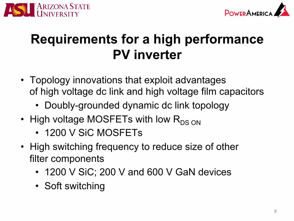
Requirements for a high performance PV inverter
• Topology innovations that exploit advantages of high voltage dc link and high voltage film capacitors
• Doubly-grounded dynamic dc link topology • High voltage MOSFETs with low RDS ON
• 1200 V SiC MOSFETs • High switching frequency to reduce size of other
filter components • 1200 V SiC; 200 V and 600 V GaN devices • Soft switching
8
Company Logo
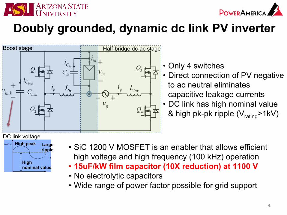
Doubly grounded, dynamic dc link PV inverter
9
gv
1Q
2Q
3Q
4Q
gi invLbLlinkv linkClinkCi
bL
ini
invinCiinC
bi
DC link voltage High peak
High nominal value
Large ripple
• Only 4 switches • Direct connection of PV negative
to ac neutral eliminates capacitive leakage currents
• DC link has high nominal value & high pk-pk ripple (Vrating>1kV)
• SiC 1200 V MOSFET is an enabler that allows efficient high voltage and high frequency (100 kHz) operation
• 15uF/kW film capacitor (10X reduction) at 1100 V • No electrolytic capacitors • Wide range of power factor possible for grid support
Boost stage Half-bridge dc-ac stage
Company Logo
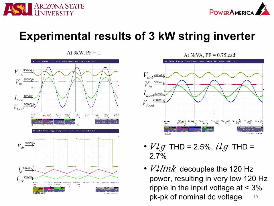
Experimental results of 3 kW string inverter
10
linkV
inV
loadI
loadV
• 𝑉↓𝑔 THD = 2.5%, 𝑖↓𝑔 THD = 2.7%
• 𝑉↓𝑙𝑖𝑛𝑘 decouples the 120 Hz power, resulting in very low 120 Hz ripple in the input voltage at < 3% pk-pk of nominal dc voltage
At 3kW, PF = 1
linkVinVloadIloadV
At 3kVA, PF = 0.75lead
350V/div
350V/div
10A/div
100V/div
350V/div
350V/div
20A/div
200V/div
dsv
biinvi
200V/div
20A/div
20A/div
Company Logo
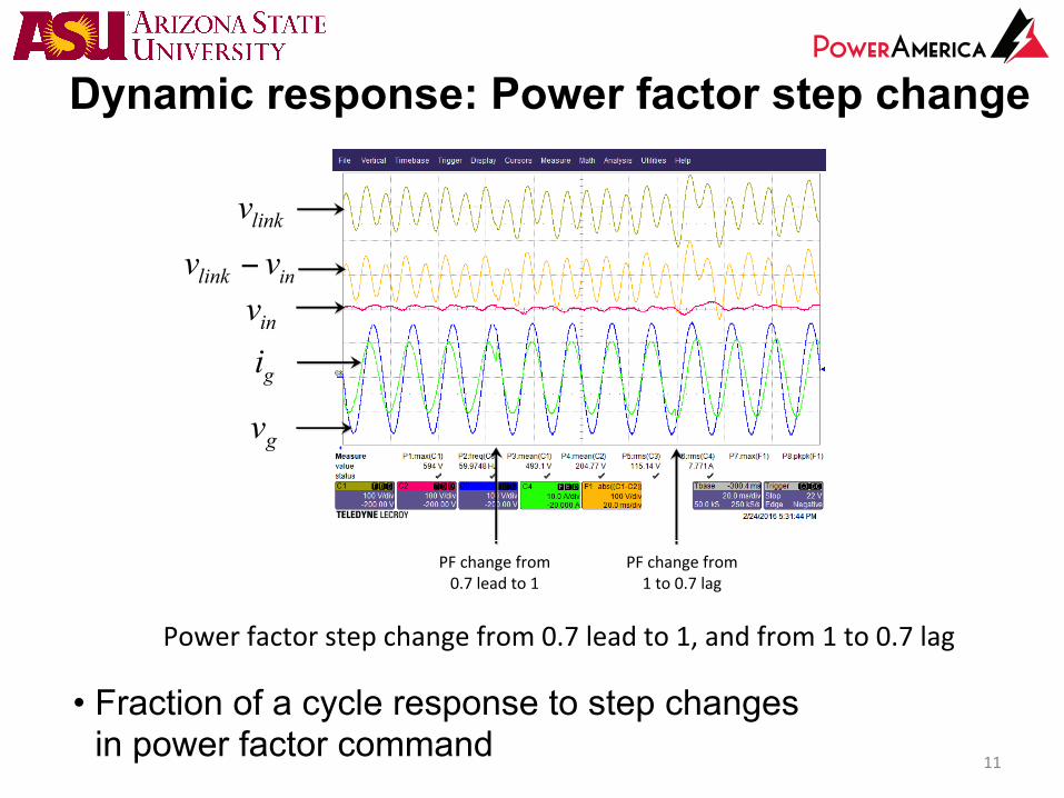
Dynamic response: Power factor step change
11
• Fraction of a cycle response to step changes in power factor command
linkv
inv
gi
gv
inlinkv v−
PF change from 0.7 lead to 1
PF change from 1 to 0.7 lag
Power factor step change from 0.7 lead to 1, and from 1 to 0.7 lag
Company Logo
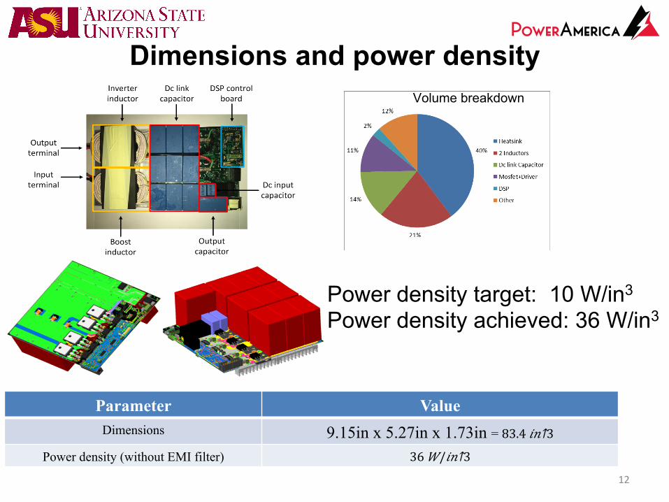
Dimensions and power density
12
Parameter Value Dimensions 9.15in x 5.27in x 1.73in = 83.4 𝑖𝑛↑3
Power density (without EMI filter) 36 𝑊/𝑖𝑛↑3
Volume breakdown
Power density target: 10 W/in3 Power density achieved: 36 W/in3
Company Logo
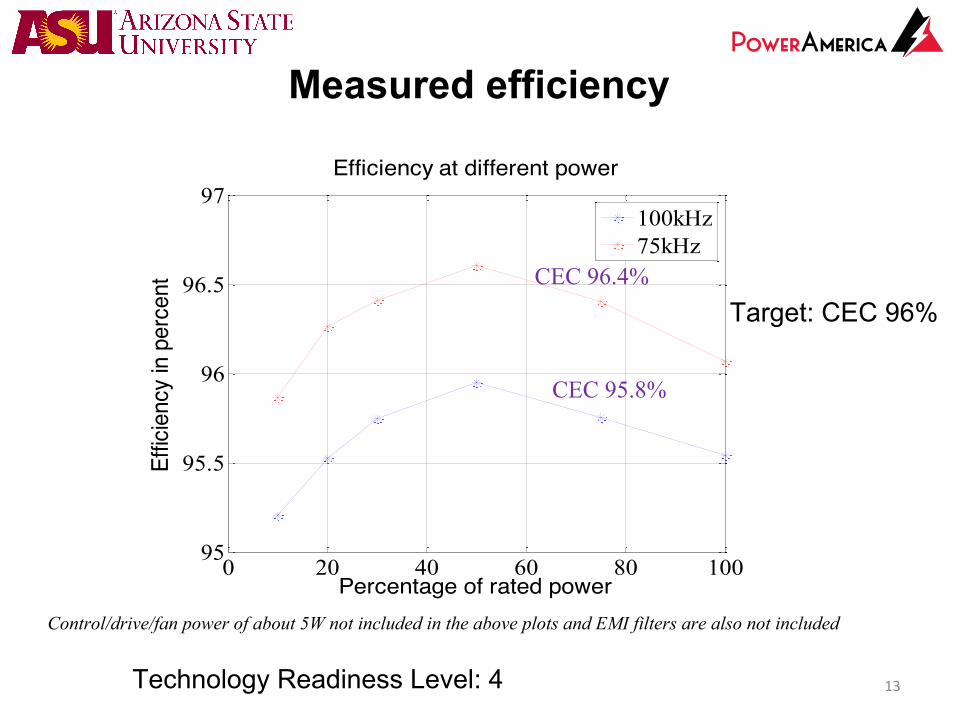
Measured efficiency
13
0 20 40 60 80 10095
95.5
96
96.5
97Efficiency at different power
Percentage of rated power
Effic
iency
in p
erce
nt
100kHz75kHz
Control/drive/fan power of about 5W not included in the above plots and EMI filters are also not included
CEC 96.4%
CEC 95.8%
Target: CEC 96%
Technology Readiness Level: 4
Company Logo
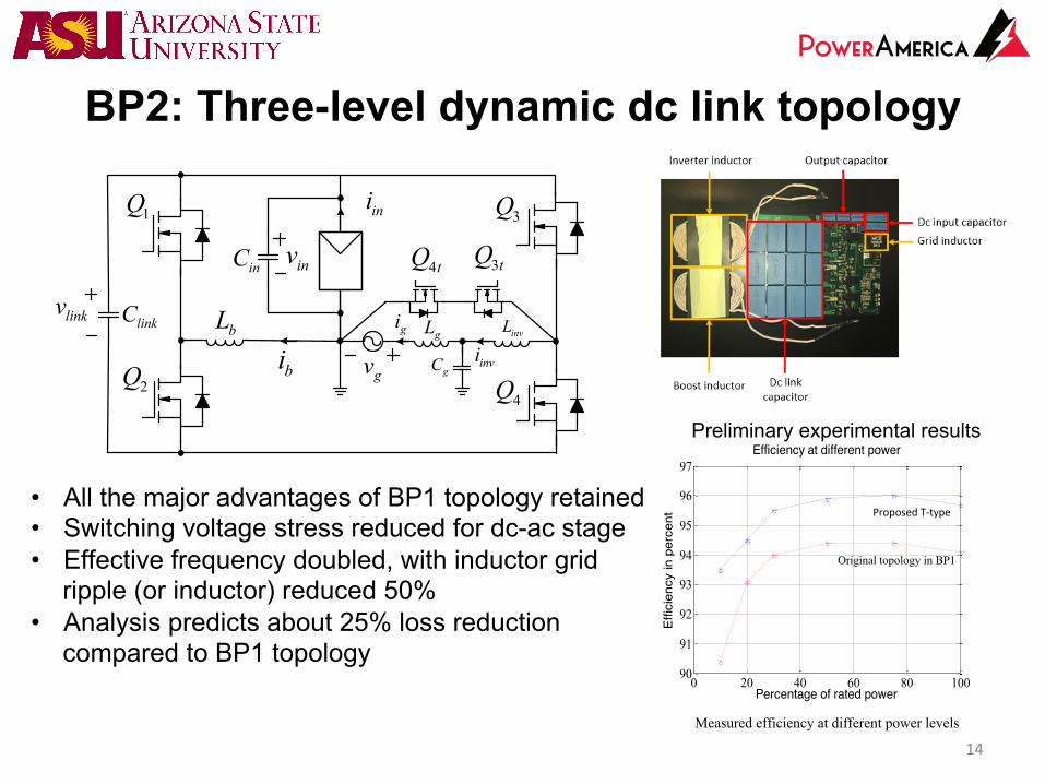
BP2: Three-level dynamic dc link topology
14
invL
invi
ini
linkClinkvbL
bi
3tQ4tQ
3Q
4Q
1Q
2Q
gi
gv
inC inv
gL
gC
• All the major advantages of BP1 topology retained • Switching voltage stress reduced for dc-ac stage • Effective frequency doubled, with inductor grid
ripple (or inductor) reduced 50% • Analysis predicts about 25% loss reduction
compared to BP1 topology
Measured efficiency at different power levels
0 20 40 60 80 10090
91
92
93
94
95
96
97Efficiency at different power
Percentage of rated power
Effic
ienc
y in
per
cent Proposed T-‐type
Original topology in BP1
Preliminary experimental results
Company Logo
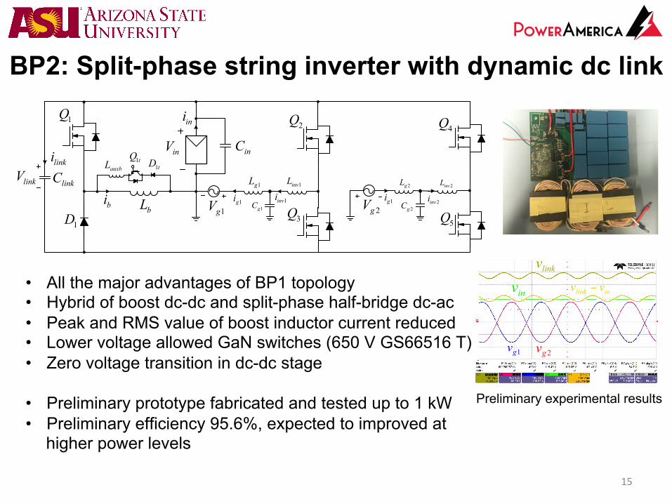
BP2: Split-phase string inverter with dynamic dc link
15
1gV 2gV
4Q
5Q
2Q
3Q
ini
1D
1Q
linki
linkClinkV
bi bL
auxbL 1tQ1tD
inV inC
1gi1invL
1invi1gL
1gC1gi
2invL
2invi2gL
2gC
• All the major advantages of BP1 topology • Hybrid of boost dc-dc and split-phase half-bridge dc-ac • Peak and RMS value of boost inductor current reduced • Lower voltage allowed GaN switches (650 V GS66516 T) • Zero voltage transition in dc-dc stage
• Preliminary prototype fabricated and tested up to 1 kW • Preliminary efficiency 95.6%, expected to improved at
higher power levels
linkv
1gv 2gv
inv inlink vv −
Preliminary experimental results
Company Logo
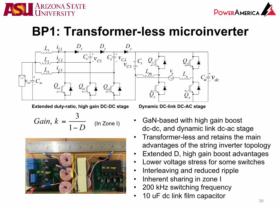
BP1: Transformer-less microinverter
16
Extended duty-ratio, high gain DC-DC stage Dynamic DC-link DC-AC stage
• GaN-based with high gain boost dc-dc, and dynamic link dc-ac stage
• Transformer-less and retains the main advantages of the string inverter topology
• Extended D, high gain boost advantages • Lower voltage stress for some switches • Interleaving and reduced ripple • Inherent sharing in zone I • 200 kHz switching frequency • 10 uF dc link film capacitor
3,1
Gain kD
=−
(In Zone I)
Company Logo
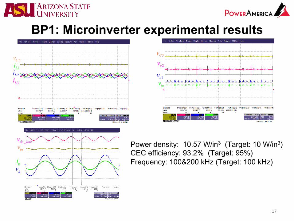
BP1: Microinverter experimental results
17
Input side interleaved inductor currents Voltage waveforms at input, output, and intermediate boost stages
Power density: 10.57 W/in3 (Target: 10 W/in3) CEC efficiency: 93.2% (Target: 95%) Frequency: 100&200 kHz (Target: 100 kHz)
3Li
1Li3Cv
2Li2cv
inv1cv
3Cv
_dc linkv
gi
inv
gv
Company Logo
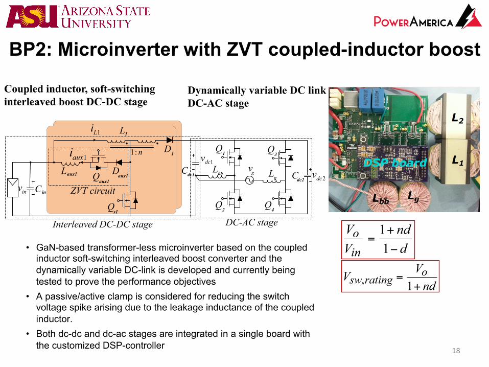
BP2: Microinverter with ZVT coupled-inductor boost
18
Coupled inductor, soft-switching interleaved boost DC-DC stage
Dynamically variable DC link DC-AC stage
Qs1
L1
Qaux1
Laux1
1Li
inv C in
D1
Cdc1
Q1
Q2
Lbb
Q3
Q4
Cdc2Lgvg
1dcv
2dcv
Interleaved DC-DC stage DC-AC stage
1: n1auxi
Daux1
ZVT circuit
• GaN-based transformer-less microinverter based on the coupled inductor soft-switching interleaved boost converter and the dynamically variable DC-link is developed and currently being tested to prove the performance objectives
• A passive/active clamp is considered for reducing the switch voltage spike arising due to the leakage inductance of the coupled inductor.
• Both dc-dc and dc-ac stages are integrated in a single board with the customized DSP-controller
11
oin
V ndV d
+=
−
, 1o
sw ratingVVnd
=+
Company Logo
Publications from BP1 and BP2 work
19
1. J. Roy; R. Ayyanar, "Sensor-less Current Sharing Over Wide Operating Range for Extended-Duty-Ratio Boost Converter," in IEEE Transactions on Power Electronics , vol.PP, no.99, pp.1-1 (Available at IEEE Early Access)
2. Y. Xia; J. Roy; R. Ayyanar, "A capacitance-minimized, doubly grounded transformer-less photovoltaic inverter with inherent active-power decoupling," in IEEE Transactions on Power Electronics , vol.PP, no.99, pp.1-1, doi: 10.1109/TPEL.2016.2606344 (Available at IEEE Early Access)
3. J. Roy; R. Ayyanar, "GaN based high gain non-isolated DC-DC stage of microinverter with extended-duty-ratio boost," in 2016 IEEE Energy Conversion Congress and Exposition (ECCE), presented, Sept 2016.
4. Y. Xia and R. Ayyanar, " Adaptive Dc Link Voltage Control Scheme for Single Phase Inverters with Dynamic Power Decoupling," 2016 IEEE Energy Conversion Congress and Exposition (ECCE), Milwaukee, WI, 2016, pp. 1-6.
5. J. Roy; Y. Xia; R. Ayyanar, "A single phase transformerless string inverter with large voltage swing of half bridge capacitors for active power decoupling," in 2016 IEEE Energy Conversion Congress and Exposition (ECCE), presented, Sept 2016.
6. Y. Xia; J. Roy; R. Ayyanar, " A High Performance T-type Single Phase Double Grounded Transformer-less Photovoltaic Inverter with Active Power Decoupling," 2016 IEEE Energy Conversion Congress and Exposition (ECCE), Milwaukee, WI, 2016, pp. 1-6.
7. Y. Xia and R. Ayyanar, "High performance ZVT with bus clamping modulation technique for single phase full bridge inverters," 2016 IEEE Applied Power Electronics Conference and Exposition (APEC), Long Beach, CA, 2016, pp. 3364-3369.
8. J. Roy, “Wide band-gap devices based solar inverters,” presented in Clean Energy Education and Empowerment (C3E) Women in Clean Energy Symposium, 2016, Stanford University, CA, USA.
9. Y. Xia and R. Ayyanar, "Inductor Feedback ZVT based, Low THD Single Phase Full Bridge Inverter with Hybrid Modulation Technique," 2017 IEEE Applied Power Electronics Conference and Exposition (APEC), March 2017 (accepted and to be presented).
10. Y. Xia; J. Roy; R. Ayyanar, "A GaN based doubly grounded, reduced capacitance transformer-less split phase photovoltaic inverter with active power decoupling," accepted in 2017 IEEE Applied Power Electronics Conference and Exposition (APEC), March 2017 (accepted and to be presented).
11. Y. Xia and R. Ayyanar, "Comprehensive Comparison of THD and Common Mode Leakage Current of Bipolar, Unipolar and Hybrid Modulation Schemes for Single Phase Grid Connected Full Bridge Inverters," 2017 IEEE Applied Power Electronics Conference and Exposition (APEC), March 2017 (accepted and to be presented).
12. J. Roy; Y. Xia and R. Ayyanar, "GaN Based Transformer-less Microinverter with Extended-Duty-Ratio Boost and Doubly Grounded Voltage Swing Inverter," 2017 IEEE Applied Power Electronics Conference and Exposition (APEC), March 2017 (accepted and to be presented).
13. J. Roy; R. Ayyanar, "A single phase transformer-less string inverter with integrated magnetics and active power decoupling," accepted in 2017 IEEE Applied Power Electronics Conference and Exposition (APEC), March 2017 (accepted and to be presented).
Company Logo
20
• Barriers to further maturity • Challenges with high frequency magnetics especially for
the transformer-isolated microinverter • Layout and reliable assembly of some special packages
Pathway to Market • High performance of both the topology and SiC/GaN devices
demonstrated on realistic prototypes • Impact on system level cost reduction through increased efficiency,
smaller filters, heatsinks and enclosures • Patent for original dynamic link topology awarded recently, and a
new patent pending for the topological enhancements, and available for licensing opportunities
Patent awarded: R. Ayyanar, “CIRCUITS AND METHODS FOR PHOTOVOLTAIC INVERTERS,” U.S. Patent 9,413,269, Aug. 2016 Patent pending: R. Ayyanar, Y. Xia, and J. Roy, “POWER CONVERTER CIRCUITRY FOR PHOTOVOLTAIC DEVICES,” Patent pending, Application No. PCT/US16/64930, filed on 12/05/2016
Company Logo
21
• Validation of commercial WBG devices in real applications with operation near rated voltages
• Validation of WBG-enabled performance enhancements in PV applications and risk mitigation
• New topologies that fully exploit WBG characteristics • Training of 4 research students and >100 course students,
and dissemination through short videos
Broader Impact on the WBG Community
• Completion of transformer-less string inverter at 240V and a separate split-phase interface with >30 W/in3 and 97% CEC, and grid support using three-level dynamic link topology and integrated magnetics
• Completion of high performance microinverter with tapped-inductor, zero voltage transition (ZVT) topology at 200 kHz
Future Direction