Embed Size (px)
Citation preview
Institut für Physikalische Elektronik
Institute of Physical Electronics
Universität Stuttgart
Jahresbericht
Annual Report
2003
Institut für Physikalische Elektronik Pfaffenwaldring 47 Redaktion/edited by: D-70569 Stuttgart Hans-Werner SchockTel.: +49-711-685-7141 Uwe Rau Fax: +49-711-685-7143 Fritz Pfisterer http://www.ipe.uni-stuttgart.de Jürgen H. Werner
Institut für Physikalische Elektronik / Institute of Physical Electronics
2
Inhaltsverzeichnis / Table of Contents
1 Vorwort / Preface
4
2 Lehre am ipe / Teaching at the ipe 6
2.1 Vorlesung Bauelemente der Mikroelektronik I ............................................2.2 Vorlesung Festkörperelektronik I ................................................................. 2.3 Vorlesung Optoelectronic Devices and Circuits I (Optoelektronik I) .............2.4 Vorlesung Photovoltaics ..............................................................................2.5 Vorlesung Energiewandlung ........................................................................2.6 Vorlesung Lasers and Light Sources ...........................................................2.7 Vorlesung Thin Film Characterization Methods ............................................2.8 Praktika ........................................................................................................
66788
101011
3 Menschen am ipe / People at the ipe 12
3.1 Verwaltung, Werkstatt und Institutsleitung / Administration, Workshop, and Head of Institute .......................................3.2 Gruppe Silicium / Group Silicon ....................................................................3.3 Gruppe Verbindungshalbleiterschichten / Group Compound Semiconductor Films ......................................................3.4 Gruppe Laserprozesse / Group Laser Processing ........................................3.5 Gruppe CIS Technologie und Oberflächenanalyse / Group CIS Technology and Surface Analysis .............................................. 3.6 Gruppe Bauelementanalyse / Group Device Analysis ..................................
1314
1618
2022
Jahresbericht 2003 / Annual Report 2003
3
4 Wissenschaftliche Beiträge / Scientific Contributions 24
U. RAU: Role of the Cu(In,Ga)Se2 Surface Defect.Layer..........................................J.H. WERNER: Efficiency Limitations of Cu(In,Ga)Se2 Solar Cells.............................T. SCHLENKER: Grain Growth in Thin Cu(In,Ga)Se2 Films..........................................G. HANNA: Film Texture and Grain Boundary Activity in Cu(In,Ga)Se2 Films...........K. ORGASSA: Optical Constants of Cu(In,Ga)Se2 Thin Films......................................G. C. GLÄSER: Analysis of Granular CuInSe2 by Electron Beam Induced Current....P.O. GRABITZ: Mechanical Properties of Flexible Cu(In,Ga)Se2 Solar Cells..............G. BILGER: Cu(In,Ga)Se2 Layers Analyzed by Corrected SIMS Depth Profiles......A. ESTURO-BRETON: Laser-Doping of n+-type Silicon Solar Cell Emitters.................C. BERGE: Monocrystalline Transfer Silicon with 150 mm Diameter.......................M. SCHUBERT: Recent Developments in Integrated Photovoltaics..........................K. TARETTO: Expression for the Current/Voltage Characteristics of pin Solar Cells..G. KRON: The Built-in Voltage and the Fill Factor of Dye Sensitized Solar Cells......
24262830323436384042444648
5 Verzeichnis der Publikationen / List of Publications 50
6 Promotionen 2003 / Ph.D. Theses 2003 53
7 Diplomarbeiten 2003 / Diploma Thesis Projects 2003 54
8 Studienarbeiten 2003 / Major Term Projects 2003 55
9 ipe Kolloquium 2003 56
10 Gäste und ausländische Stipendiaten / Guests 57
11 Wissenschaftliche Geräte und Analysemethoden
/ Scientific Instruments and Methods of Analysis
11.1 Abscheideverfahren / Deposition Methods ................................................11.2 Strukturelle Analyseverfahren / Structural Materials Analysis ....................11.3 Analyse optischer Eigenschaften / Analysis of Optical Properties .............11.4 Analyse elektro-optischer Eigenschaften / Electro-optical Properties ........
59
59 60 61 62
12 Mitarbeiterliste / Staff Members 63
13 Lageplan / Site Plan 66
Institut für Physikalische Elektronik / Institute of Physical Electronics
4
1 Vorwort
Liebe Freunde des ipe,
Sie halten hier den Siebten der Jahresberichte des ipe in Händen;
wir informieren Sie über unsere Arbeit im Jahr 2003. Wer die Berichte in den letzten Jahren aufmerksam verfolgt hat, wird bemerkt haben, dass wir uns immer mehr auf unser Kerngeschäft konzentrierten: Physik und Technologie der Halbleitermaterialien und -bauelemente. Nur so können wir unseren Standard in der immer härteren Konkurrenz um erstklassiges Personal und um Forschungsgelder halten.
Die Stärke des ipe ist es, Grundlagenforschung mit der Anwendung bis hin zur direkten Kooperation mit der Industrie zu verbinden. Unser Drittmittelumsatz von über 2,5 Millionen Euro mit 20% direktem Industrieanteil spricht für sich. Über 35 der derzeit 47 Mitarbeiter/innen (ohne Studenten, ohne Gäste) des ipe werden aus diesen Drittmitteln bezahlt. Dennoch haben im Jahr 2003 am ipe wieder 8 junge Wissenschaftler in einer Zeit von etwa 3 ½ Jahren promoviert.
Im Jahr 2003 haben sich zehn deutsche Universitätsinstitute, die auf dem Gebiet der Photovoltaik forschen, zum Forschungsverbund PV-Uni-Netz zusammen geschlossen. Ziel des Verbundes ist es, die Forschung besser zu koordinieren und nach außen hin besser darzustellen. Zur Zeit fungiere ich selbst als Sprecher dieses Verbundes. Wir werden sehen, ob dieser Zusammenschluss zu einer Stärkung der Photovoltaik-Forschung an deutschen Universitäten führen wird.
Ich bedanke mich an dieser Stelle ganz herzlich bei allen Mitarbeitern des ipe, meinen Kollegen in der Fakultät, meinen Freunden sowie der Leitung und Verwaltung der Universität Stuttgart für die Unterstützung meiner Forschung und Lehre der letzten 7 ½ Jahre.
Stuttgart, Dezember 2003
Jürgen H. Werner
Jahresbericht 2003 / Annual Report 2003
5
1 Preface
Dear friends of the ipe,
You are holding in your hands the seventh Annual Report of the
ipe; we are informing you about our work during the year 2003. Those who have followed our annual reports in the last years will notice that we concentrate more and more on our main expertise: Physics and Technology of Semiconductor Materials and Devices. This is the only way to maintain our high standard in the increasingly harder competition for first class staff and for research funds.
The strength of the ipe lies in combining basic research with applications and direct cooperation with industry. Our annual turnover of more than 2.5 million Euros with a 20% share of direct industry funding speaks for itself. More than 35 persons of our staff at present (a total of 47 persons, students and guests not included) are being paid from research funds. Nevertheless, in 2003 again 8 young scientists completed their PhD-thesis within about 3 ½ years.
In the year 2003, ten German university institutes engaged in photovoltaics research formed the research network PV-Uni-Netz. This network aims at improved research coordination and at a better presentation of research results to the public. At present, I have the honour of being the speaker of this association. We shall see whether this joining together yields a reinforcement of the photovoltaics research at German Universities.
At this place, I would like to express my sincere thanks to the whole ipe staff, to my colleagues of the Faculty, to my friends and to the rector and administration of the Stuttgart University for the support given to my research and teaching work during the last 7 ½ years.
Stuttgart, December 2003
Jürgen H. Werner
Institut für Physikalische Elektronik / Institute of Physical Electronics
6
2 Lehre am ipe / Teaching at the ipe
2.1 Vorlesung Bauelemente der Mikroelektronik Einführung: Diverse Informationen; Geschichte der Halbleiterbauelemente;
Mikroelektronik heute. Leitfähigkeit und Energiebänder: Spezifischer Widerstand; Energiebänder. Silicium – der Werkstoff der Mikroelektronik: Periodensystem der Elemente;
Element Si; Siliciumkristalle; Herstellung von hochreinen Siliciumscheiben; Siliciumdioxid als Schutzschicht für Silicium; Herstellung einer integrierten Schaltung durch Planarprozess; kleinere Strukturen und größere Scheiben (Wafer); Dotieren von Silicium.
Elektronen und Löcher in Halbleitern: Das Loch als Quasiteilchen; Ladung des Loches; Energie von Elektronen und Löchern; effektive Masse m*;
elektrisches Feld ε und Potential ϕ. Ströme in Halbleitern: Leitfähigkeit σ; Ladungsträgerkonzentrationen n, p in den
Bändern; Beweglichkeit; Spezifischer Widerstand; Diffusionströme Jdiff ; Gesamtstrom im Halbleiter.
Nichtgleichgewicht und Injektion: Rekombination und Generation; Quasi-Fermi-Niveaus (QFN oder Imref).
Elektrostatik des pn-Übergangs: Prinzip der pn-Diode; Ladungsträgerkonzentratio-
nen im Gleichgewicht; Diffusionsspannung Vbi ; elektrisches Feld ε, Potential ϕ, Raumladung ρQ ; Kenngrößen des pn-Übergangs.
Ströme im pn-Übergang: Feld- und Diffusionsströme; Kennlinie des idealen pn-Überganges; Kapazität, Kleinsignalwiderstand und Kleinsignalersatzschaltbild des pn-Übergangs; Grenzen der idealen Diodentheorie.
Anhang: Ergänzungen zur Vorlesung: Photonenenergie und Wellenlänge von Strahlung; Messung der Bandlücke Eg ; Temperaturabhängigkeit der Bandlücke; Fermi-Niveaus des extrinsischen Halbleiters bei unbekannter Ladungsträgerkonzentration; Sättigungsgeschwindigkeit vsat ; Einfluss der Dotierung(-shöhe) auf µn , µp ; Einfluss der Temperatur auf µn, µp .
Jahresbericht 2003 / Annual Report 2003
7
2.2 Vorlesung Solid State Electronics
Band Model of Semiconductors: Band gap Eg and conductivity; electron concentration in conduction band.
Free Electrons as Waves: Particle properties of electrons; Davisson and Germer´s experiment (1927); Bragg´s diffraction condition; de Broglie´s hypothesis; small and large particles and solids; condition for observation of wave properties; breakdown of classic wave/particle picture; structure analysis of solids; wave function ψ of de-Broglie waves (particle waves); Schroedinger's equation; free electron revisited in view of Schroedinger equation.
Electrons in Idealized Solids: One-dimensional potential box of size L (particle in a box); electrons in three-dimensional potential well; Fermi-distribution.
Electrons in Real Crystals: Bloch waves; band structure of some important semiconductors; the “Brillouin-Zone”, reciprocal lattice vectors; allowed k-values; states per band; empty and full bands.
Band Structure and Band Model: Band structure of Si, Ge, GaAs; three-dimensional delineation; from band structure E(k) to band model/diagram; metal, semiconductor, isolator; direct and indirect semiconductors; moving electrons; particle momentum pp and pseudo-crystal momentum pk; holes.
Emission of Electrons from Solids: Work function qφA, electron affinity qχ; thermal emission; tunneling, photoemission; current/voltage curve;
A1. Proof of the Richardson-Dushman-Equation.
2.3 Vorlesung Optoelectronic Devices and Circuits Introduction – What is Optoelectronics? Overlap of optoelectronics with classic
areas; optical regime; scheme of an optical communication system; what is light?
Basic Physics: Simple equations: reflectance, absorbance, transmittance; refraction and total internal reflection; reflectance rΦ, transmittance tΦ for Θi = 0.
Thermal Radiation: Black body radiation (Kirchhoff’s radiation law, Planck’s radiation law, Wien’s displacement law, Stefan-Boltzmann law); grey body radiation; selective body radiation of a semiconductor.
Coherence: Definition; length of a wave train; the frequency spectrum of a wave train.
Semiconductor Basics: Energy bands and Fermi function (wave vector k, band structure E(k), limited range of k-values, Brillouin zone, crystal momentum pk, impulse pe, direct and indirect bandgap semiconductors.
Excitation and Recombination Processes in Semiconductors: Introduction – What is luminescence? Absorption of radiation in semiconductors; carrier recombination in semiconductors.
Light Emitting Diodes: Working principle; emitted spectrum of an LED; materials for LEDs (and lasers); emission efficiency of LEDs.
Semiconductor Lasers: Working principle; laser components; ratio of induced (stimulated) to spontaneous emission; gain of a laser (first general laser condition); the resonator; first lasing condition for semiconductor lasers;
Institut für Physikalische Elektronik / Institute of Physical Electronics
8
second lasing condition for a semiconductor laser; heterojunctions, heterostructures; light guiding in semiconductor lasers; stripe contact laser; laser modes; gain in a semiconductor laser; modern semiconductor lasers.
Glass Fibres: Advantages of glass fibers; fiber configurations; step-index-, graded-index- and mono-mode fibers; dispersion and attenuation in glass fibers.
Photodetectors: Introduction, general considerations; properties and specifications of photodetectors; photoconductors; photodiodes; photodiodes with internal gain: avalanche photodiodes (APDs); materials and detector configurations.
2.4 Vorlesung Photovoltaics Energy Data: Energy units and energy content; consumption of Germany (2000);
carbon dioxide creation; mean power for a German. The Solar Spectrum: The sun as a black body; terrestrial solar spectrum. Potential of Solar Radiation: Theoretical potential; technical potential of solar
energy world wide; technical potential of solar energy in Germany. The Principal Functions of Photovoltaic Systems. Generation and Recombination in Semiconductors: Absorption of radiation in
semiconductors; recombination. Basic Semiconductor Equations: Currents in semiconductors; generation and
recombination. pn-Junctions: The pn-junction in thermal equilibrium; pn-junction under applied
bias; the pn-junction solar cell under illumination. Current/Voltage-Curve of Solar Cells: Characteristic values and equivalent circuit of
the ideal solar cell; equivalent circuit and characteristic data of a real solar cell. Maximum Efficiency of Solar Cells: Experimental limits; loss processes; radiative
efficiency limit after Shockley & Queisser. Preparation of Crystalline Silicon: Single crystalline silicon wafers; polycrystalline
silicon wafers. Technology of Crystalline Silicon Solar Cells: Screen printing technology; high
efficiency technology. Amorphous Silicon Solar Cells: Why thin-film solar cells; material properties of
amorphous silicon; Staebler-Wronski effect; structure of an a-Si:H solar cell; preparation of a-Si:H solar cells; module and cell efficiencies; products you can buy.
Cu(In,Ga)Se2 Solar Cells: Material properties of Cu(In,Ga)Se2; structure of ZnO/CdS/Cu(In,Ga)Se2 heterojunction solar cell; variation of the composition of Cu(In,Ga)(S,Se)2 (alloying); preparation of Cu(In,Ga)Se2 solar cells; cell and module efficiencies; new developments.
Jahresbericht 2003 / Annual Report 2003
9
2.5 Vorlesung Energiewandlung
Einführung: Energie: Grundbegriffe; Energiewandlungskette, Energieträger. Kernenergie: Grundlagen: Kernkraftwerke in Deutschland und weltweit,
Atomkerne, Massendefekt, Energiegewinn durch Spaltung und Fusion, Kernumwandlungen; Kontrollierte Kernspaltung: Kettenreaktion und kritische Masse, prompte und verzögerte Neutronen, Aufbau eines Kernreaktors, Energiebilanz, Kritikalität und Reaktivität, Moderatoren, Steuerung der Kettenreaktion.
Thermodynamik: Definitionen: Energie, chemisches Potential, Verbrennung, Heizwert und Brennwert, Entropie, thermodynamische Potentiale;
Zustandsgleichungen: Ideales Gas, reale Gase; Kreisprozesse: Carnot-Prozess, weitere Kreisprozesse; Wärmekraftmaschine/Kraftwärme-maschine; Exergie; Hauptsätze der Thermodynamik; kWh(el) und kWh(therm).
Direkte Nutzung der Sonnenenergie: Der AM-Wert, das Sonnenspektrum, globale, diffuse und direkte Strahlung, Jahresgang der Globalstrahlung in Deutschland, die Sonne als schwarzer Strahler; solarthermische Energiewandlung: Niedertemperaturkollektoren, selektive Absorber, selektive Abdeckung, Kollektorwirkungsgrad; Photovoltaik: Halbleiter und Solarzellen, Lichtabsorption, Kennlinie und Wirkungsgrade, Verluste in realen Solarzellen, Dünnschichtsolarzellen, Entwicklung der Photovoltaik.
Indirekte Nutzung der Sonnenenergie: Wasserkraft: Beitrag zur Stromerzeugung, Leistung eines Wasserkraftwerks, Kraftwerksarten, Turbinenarten; Windenergie: Leistung des Windes, maximaler Wirkungsgrad eines Rotors, Widerstands- und Auftriebsläufer, Bauformen von Windkraftwerken..
Chemische Umsetzung elektrischer Energie: Galvanische Elemente; Primärelemente: Batterietypen, Anwendungen; Akkumulatoren: der Bleiakku und andere Typen; Kondensatoren: Vergleich Batterie/Kondensator, Elektrolyt- und Superkondensator; Energiedichten von Batterien, Akkus und Kondensatoren; Brennstoffzellen: Funktionsprinzip, Typen und Typenvergleich.
Institut für Physikalische Elektronik / Institute of Physical Electronics
10
2.6 Vorlesung Lasers and Light Sources
The Human Eye: Anatomy of the human eye; rerfracting power D of the human
eye; near point, far point; focusing problems; rods, cones; color vision; color deficiency.
Light and Color: Light sensitivity of the human eye; CIE color matching functions^; color coordinates X, Y, Z and color chromaticity coordinates x, y, z; chromaticity diagram; colcor mixing.
Photometry and Colorimetry: Energetic quantities of radiation and irradiation; visual quantities of light and illumination.
Incoherent Light Sources: Black body radiation; gray body radiation; selective body radiation of a semiconductor; emissivity of non-black bodies; incandescent lamps; gas discharge light sources.
Light Emitting Diodes: Working principle; the emitted spectrum of an LED; materials for LEDs (and lasers); emission efficiency of LEDs; organic light emitting diodes (OLEDs).
Lasers: Fundamental processes; occupation probability in thermodynamic equilibrium; microscopic analysis; set-up of a laser; optical resonator; line width; laser types; semiconductor lasers.
Jahresbericht 2003 / Annual Report 2003
11
2.8 Praktika. / Laboratory courses
Grundlagenpraktikum Physikalische Elektronik: im Vorstudium, WS + SS
4 Versuche: Lichtemittierende Dioden (LED), Laserdiode, Farbfernsehtechnik, Photovoltaik mit Netzeinspeisung.
Praktikum Elektrophysik: im Hauptstudium, SS
a) Praktikum Photovoltaik:
7 Versuche: Dünnschichtsolarzellen aus Verbindungshalbleitern, Teil 1: Solarzellenpräparation / Aufdampfanlage; Dünnschichtsolarzellen aus Verbindungshalbleitern, Teil 2: Absorbercharakterisierung / REM mit EDX; Elektrische Charakterisierung von Dünnschichtsolarzellen (CIS), Strom-Spannungs-Kennlinie, Bestimmung der Bandlücke Eg, spektrale Quantenausbeute; Dünnschichtsolarzellen aus amorphem Silicium, Solarzellenpräparation / CVD; Jahresenergieerträge verschiedener PV-Technologien in Europa, η(E)-Messungen an mono-c-Si-, multi-c-Si-, a-Si- und CIS-Zellen, Berechnung der Jahresenergieerträge für die Standard-Europa-Einstrahlungsverteilung; Verschaltung von Zellen zu Modulen, Abschattungsprobleme, Bypass- und Blockierdioden; Inselsystem, Solar Home System, Aufbau und Funktionstest mit SHS-Tester, Simulationsprogramm;
b) Praktikum Mikroelektronik (mit Institut für Mikroelektronik Stuttgart): 9 Versuche: Bauelementesimulation mit Atlas (Silvaco), device-Simulation el.
Parameter; Diffusion / Oxidation; Ionenimplantation / Ionen-Projektionslithographie; Lithographie; Vakuumtechnik / Metallisierung; Materialcharakterisierung / REM / EDX / EBIC; Schaltungssimulation mit SPICE; Elektr. Charakterisierung / IV / CV ..; IC-Lab (digitaler Schaltungsentwurf, Hierarchie, Netzlisten, Verifikation).
Institut für Physikalische Elektronik / Institute of Physical Electronics
12
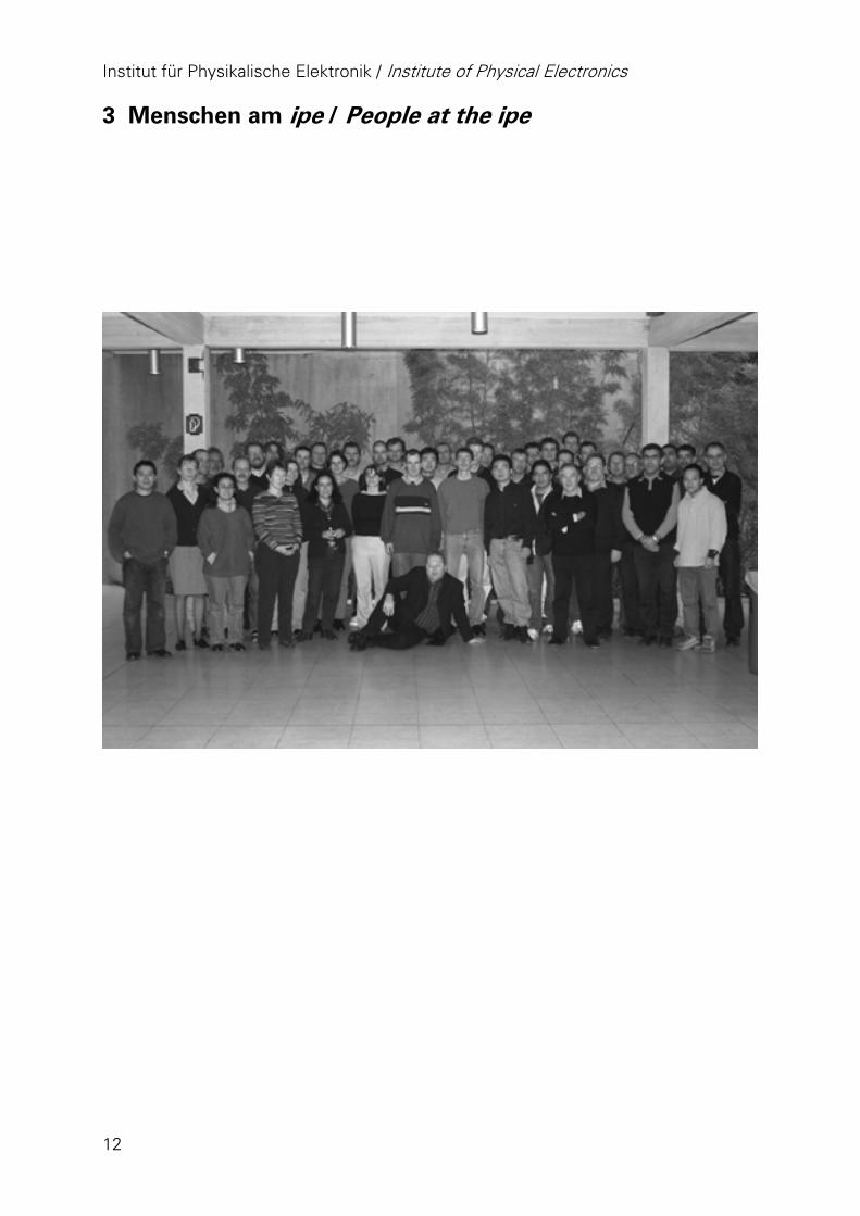
3 Menschen am ipe / People at the ipe
Jahresbericht 2003 / Annual Report 2003
13
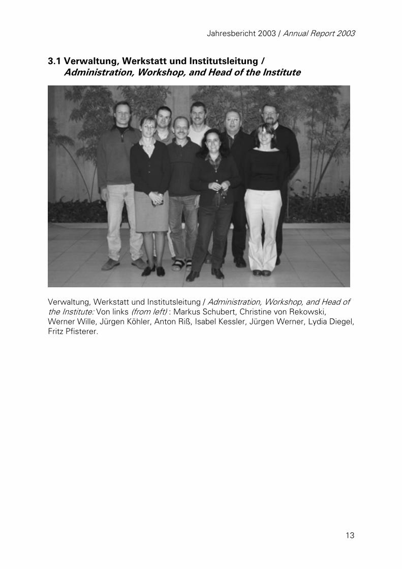
3.1 Verwaltung, Werkstatt und Institutsleitung / Administration, Workshop, and Head of the Institute
Verwaltung, Werkstatt und Institutsleitung / Administration, Workshop, and Head of the Institute: Von links (from left) : Markus Schubert, Christine von Rekowski, Werner Wille, Jürgen Köhler, Anton Riß, Isabel Kessler, Jürgen Werner, Lydia Diegel,Fritz Pfisterer.
Institut für Physikalische Elektronik / Institute of Physical Electronics
14
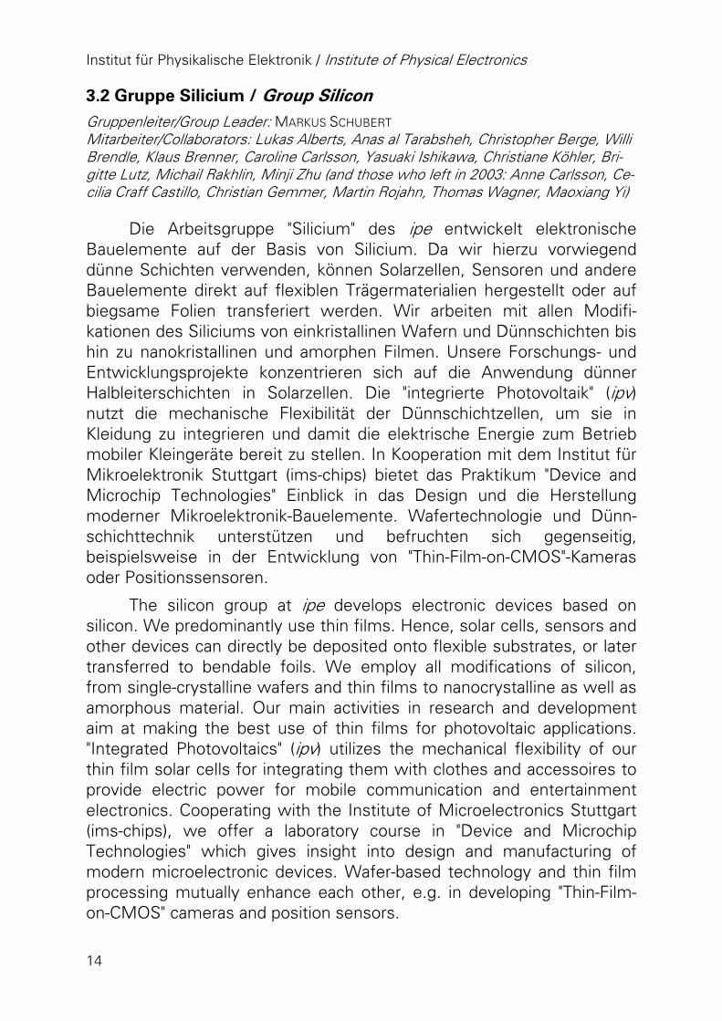
3.2 Gruppe Silicium / Group Silicon
Gruppenleiter/Group Leader: MARKUS SCHUBERT Mitarbeiter/Collaborators: Lukas Alberts, Anas al Tarabsheh, Christopher Berge, Willi Brendle, Klaus Brenner, Caroline Carlsson, Yasuaki Ishikawa, Christiane Köhler, Bri-gitte Lutz, Michail Rakhlin, Minji Zhu (and those who left in 2003: Anne Carlsson, Ce-cilia Craff Castillo, Christian Gemmer, Martin Rojahn, Thomas Wagner, Maoxiang Yi)
Die Arbeitsgruppe "Silicium" des ipe entwickelt elektronische Bauelemente auf der Basis von Silicium. Da wir hierzu vorwiegend dünne Schichten verwenden, können Solarzellen, Sensoren und andere Bauelemente direkt auf flexiblen Trägermaterialien hergestellt oder auf biegsame Folien transferiert werden. Wir arbeiten mit allen Modifi-kationen des Siliciums von einkristallinen Wafern und Dünnschichten bis hin zu nanokristallinen und amorphen Filmen. Unsere Forschungs- und Entwicklungsprojekte konzentrieren sich auf die Anwendung dünner Halbleiterschichten in Solarzellen. Die "integrierte Photovoltaik" (ipv) nutzt die mechanische Flexibilität der Dünnschichtzellen, um sie in Kleidung zu integrieren und damit die elektrische Energie zum Betrieb mobiler Kleingeräte bereit zu stellen. In Kooperation mit dem Institut für Mikroelektronik Stuttgart (ims-chips) bietet das Praktikum "Device and Microchip Technologies" Einblick in das Design und die Herstellung moderner Mikroelektronik-Bauelemente. Wafertechnologie und Dünn-schichttechnik unterstützen und befruchten sich gegenseitig, beispielsweise in der Entwicklung von "Thin-Film-on-CMOS"-Kameras oder Positionssensoren.
The silicon group at ipe develops electronic devices based on silicon. We predominantly use thin films. Hence, solar cells, sensors and other devices can directly be deposited onto flexible substrates, or later transferred to bendable foils. We employ all modifications of silicon, from single-crystalline wafers and thin films to nanocrystalline as well as amorphous material. Our main activities in research and development aim at making the best use of thin films for photovoltaic applications. "Integrated Photovoltaics" (ipv) utilizes the mechanical flexibility of our thin film solar cells for integrating them with clothes and accessoires to provide electric power for mobile communication and entertainment electronics. Cooperating with the Institute of Microelectronics Stuttgart (ims-chips), we offer a laboratory course in "Device and Microchip Technologies" which gives insight into design and manufacturing of modern microelectronic devices. Wafer-based technology and thin film processing mutually enhance each other, e.g. in developing "Thin-Film-on-CMOS" cameras and position sensors.
Jahresbericht 2003 / Annual Report 2003
15
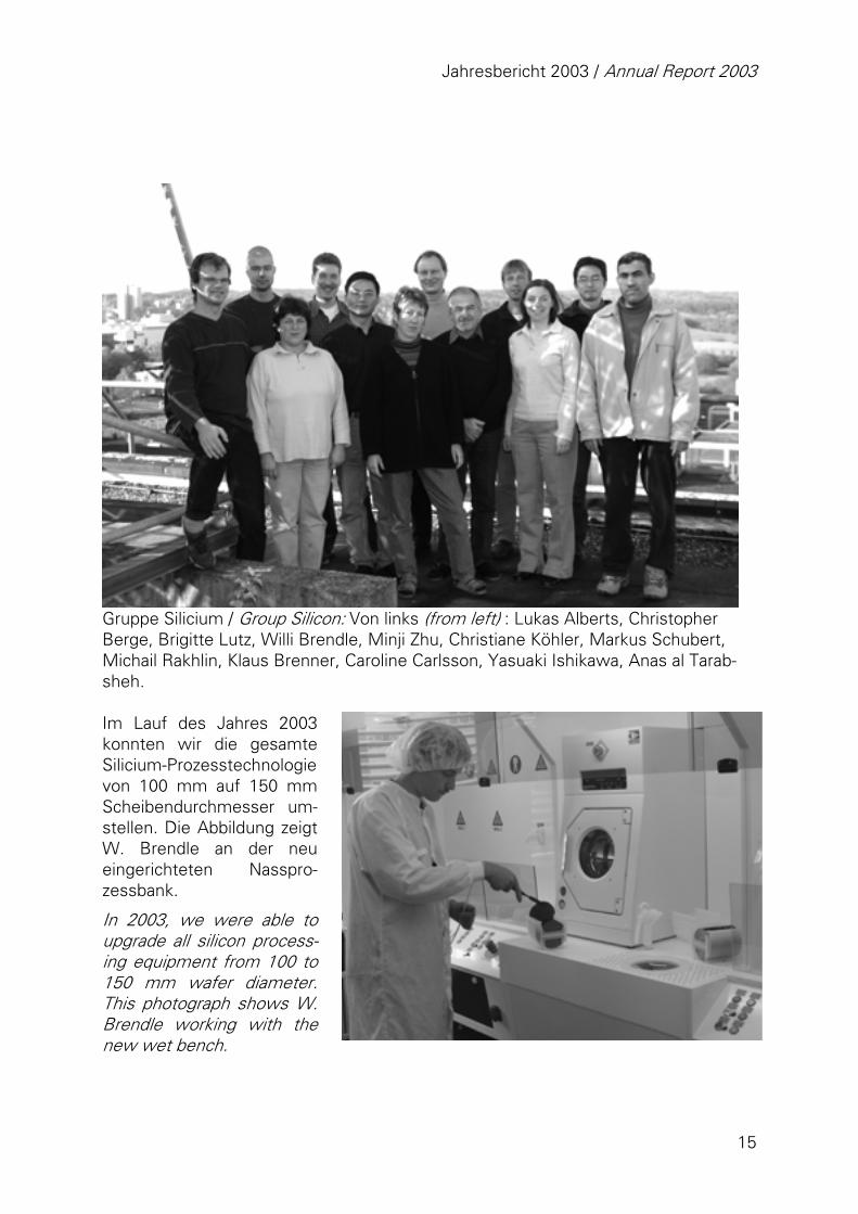
Gruppe Silicium / Group Silicon: Von links (from left) : Lukas Alberts, Christopher Berge, Brigitte Lutz, Willi Brendle, Minji Zhu, Christiane Köhler, Markus Schubert, Michail Rakhlin, Klaus Brenner, Caroline Carlsson, Yasuaki Ishikawa, Anas al Tarab-sheh. Im Lauf des Jahres 2003 konnten wir die gesamte Silicium-Prozesstechnologie von 100 mm auf 150 mm Scheibendurchmesser um-stellen. Die Abbildung zeigt W. Brendle an der neu eingerichteten Nasspro-zessbank.
In 2003, we were able to upgrade all silicon process-ing equipment from 100 to 150 mm wafer diameter. This photograph shows W. Brendle working with the new wet bench.
Institut für Physikalische Elektronik / Institute of Physical Electronics
16
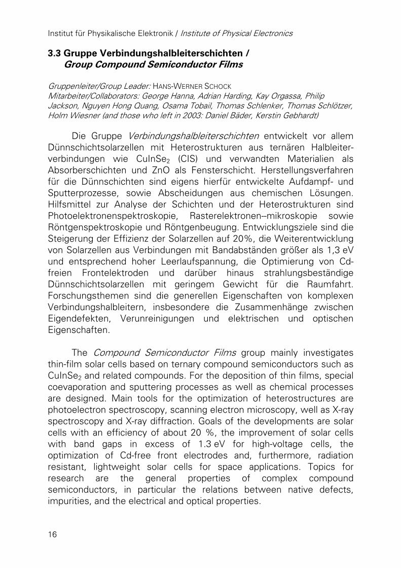
3.3 Gruppe Verbindungshalbleiterschichten / Group Compound Semiconductor Films Gruppenleiter/Group Leader: HANS-WERNER SCHOCK Mitarbeiter/Collaborators: George Hanna, Adrian Harding, Kay Orgassa, Philip Jackson, Nguyen Hong Quang, Osama Tobail, Thomas Schlenker, Thomas Schlötzer, Holm Wiesner (and those who left in 2003: Daniel Bäder, Kerstin Gebhardt)
Die Gruppe Verbindungshalbleiterschichten entwickelt vor allem Dünnschichtsolarzellen mit Heterostrukturen aus ternären Halbleiter-verbindungen wie CuInSe2 (CIS) und verwandten Materialien als Absorberschichten und ZnO als Fensterschicht. Herstellungsverfahren für die Dünnschichten sind eigens hierfür entwickelte Aufdampf- und Sputterprozesse, sowie Abscheidungen aus chemischen Lösungen. Hilfsmittel zur Analyse der Schichten und der Heterostrukturen sind Photoelektronenspektroskopie, Rasterelektronen--mikroskopie sowie Röntgenspektroskopie und Röntgenbeugung. Entwicklungsziele sind die Steigerung der Effizienz der Solarzellen auf 20%, die Weiterentwicklung von Solarzellen aus Verbindungen mit Bandabständen größer als 1,3 eV und entsprechend hoher Leerlaufspannung, die Optimierung von Cd-freien Frontelektroden und darüber hinaus strahlungsbeständige Dünnschichtsolarzellen mit geringem Gewicht für die Raumfahrt. Forschungsthemen sind die generellen Eigenschaften von komplexen Verbindungshalbleitern, insbesondere die Zusammenhänge zwischen Eigendefekten, Verunreinigungen und elektrischen und optischen Eigenschaften.
The Compound Semiconductor Films group mainly investigates
thin-film solar cells based on ternary compound semiconductors such as CuInSe2 and related compounds. For the deposition of thin films, special coevaporation and sputtering processes as well as chemical processes are designed. Main tools for the optimization of heterostructures are photoelectron spectroscopy, scanning electron microscopy, well as X-ray spectroscopy and X-ray diffraction. Goals of the developments are solar cells with an efficiency of about 20 %, the improvement of solar cells with band gaps in excess of 1.3 eV for high-voltage cells, the optimization of Cd-free front electrodes and, furthermore, radiation resistant, lightweight solar cells for space applications. Topics for research are the general properties of complex compound semiconductors, in particular the relations between native defects, impurities, and the electrical and optical properties.
Jahresbericht 2003 / Annual Report 2003
17
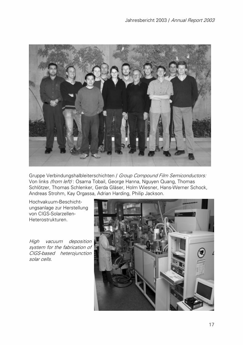
Gruppe Verbindungshalbleiterschichten / Group Compound Film Semiconductors: Von links (from left) : Osama Tobail, George Hanna, Nguyen Quang, Thomas Schlötzer, Thomas Schlenker, Gerda Gläser, Holm Wiesner, Hans-Werner Schock, Andreas Strohm, Kay Orgassa, Adrian Harding, Philip Jackson.
Hochvakuum-Beschicht-ungsanlage zur Herstellung von CIGS-Solarzellen-Heterostrukturen.
High vacuum deposition system for the fabrication of CIGS-based heterojunction solar cells.
Institut für Physikalische Elektronik / Institute of Physical Electronics
18
3.4 Gruppe Laserprozesse / Group Laser Processing
Gruppenleiter/Group Leader: JÜRGEN R. KÖHLER Mitarbeiter/Collaborators: Ainhoa Esturo-Breton (and who left in 2003: Jakob Demir)
Die Gruppe Laserprozesse entwickelt neue Technologien zur Laserprozessierung der am ipe verwendeten einkristallinen und polykristallinen Halbleiter. Hierzu zählen die Strukturierung der Halbleiter, deren Kristallisation und Rekristallisation sowie die Laser-Dotierung zur Herstellung von Emittern und Rückseitenkontakten für einkristalline Silicium-Solarzellen. Im Vordergrund unserer Arbeiten stehen Grundlagenuntersuchungen zur Laserdotierung von einkristallinem Silicium. Entwicklungsziele sind die Erhöhung des Durchsatzes bei der laserunterstützten Emitterdotierung sowie die Steigerung der Wirkungsgrade von 100 mm x 100 mm großen einkristallinen Silicium-Solarzellen auf über 17%.
The laser processing group explores new technologies for laser processing of monocrystalline and polycrystalline semiconductors. Examples are laser structuring, laser annealing, laser crystallization and laser doping of monocrystalline silicon. The main topic of our research work is the investigation of the fundamental processes involved in a pulsed laser doping process for the preparation of n+-doped emitters on monocrystalline silicon wafers. Development goals are the increase of the throughput rate of the laser doping process as well as the increase of the efficiency of 100 mm x 100 mm sized moncrystalline silicon solar cells to more than 17%.
Jahresbericht 2003 / Annual Report 2003
19
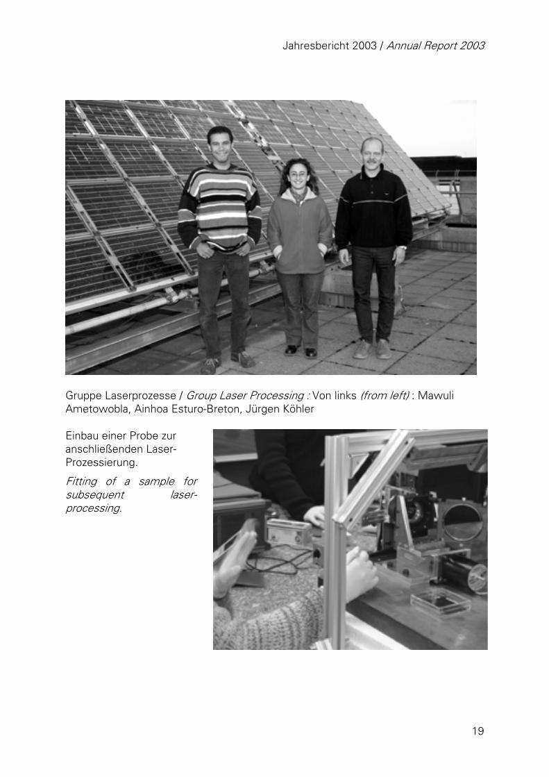
Gruppe Laserprozesse / Group Laser Processing : Von links (from left) : Mawuli Ametowobla, Ainhoa Esturo-Breton, Jürgen Köhler Einbau einer Probe zur anschließenden Laser-Prozessierung.
Fitting of a sample for subsequent laser-processing.
Institut für Physikalische Elektronik / Institute of Physical Electronics
20
3.5 Gruppe CIS-Technologie und Oberflächenanalyse / Group CIS Technology and Surface Analysis Gruppenleiter/Groupleader: GERHARD BILGER Mitarbeiter/Collaborators: Leo Bauer, Lorenz Eisenmann, Peter Grabitz, Denis Kühnle, Viktor Laptev, Martin Wagner (and who left in 2003: Thomas Dolch)
Die bei der Oberflächenanalyse angewandten Methoden sind die Sekundärionen-Massenspektrometrie (SIMS) sowie die Röntgen- und Ultraviolett-Photoelektronen-Spektrometrie (XPS, UPS). Die Analytik unterstützt die Gruppen, die Forschung und Entwicklung an Materialien für die Photovoltaik und Sensorik am ipe betreiben. Nach außen werden diese Analytikmethoden als Dienstleistungen für die Industrie und andere Institute angeboten. Als sehr empfindliche Methode weist SIMS alle Elemente und deren Verbindungen bis in den ppb-Bereich nach. Tiefen- und ortsaufgelöste Analysen zeigen den Verlauf von Element-verteilungen in einer Schichtfolge und/oder deren laterale Verteilung. XPS-Analysen, empfindlich bis in den 0,1 Atom%-Bereich, sind quanti-tativ und geben Auskunft über Bindungszustände der Elemente. Die extrem oberflächensensitive Methode weist noch Oberflächenbe-deckungen von 1/10 einer Monolage nach. Mit UPS wird die Valenzband-struktur von Festkörpern untersucht. Bei der CIS Technologie liegt die Verantwortung für die Durchführung routinemäßiger Schicht-präparationen und den Unterhalt der dafür notwendigen Infrastruktur.
For Surface Analysis the methods applied are Secondary Ion Mass Spectrometry (SIMS) and X-ray- and Ultraviolet-Photoelectron Spectrometry (XPS, UPS). These methods support the work of the groups at the Institute of Physical Electronics involved in research and development of materials for photovoltaics and sensors. Analyses are also offered as a service to other institutes and to industry as well. The method SIMS is very sensitive to the detection of all elements and their compositions with concentrations down to the ppb region. SIMS detects the distribution of elements in layers laterally resolved and/or in their depth. The analysis technique XPS is quantitative down to a concentration of 0.1 atomic % and gives information about the chemical binding state. XPS detects surface coverages down to 1/10 of a monolayer. The method UPS is applied to study the structure of the valence band in solids. CIS Technology includes the routine preparation of CuInSe2 thin films for solar cells and the maintenance of the infrastructure necessary for it.
Jahresbericht 2003 / Annual Report 2003
21
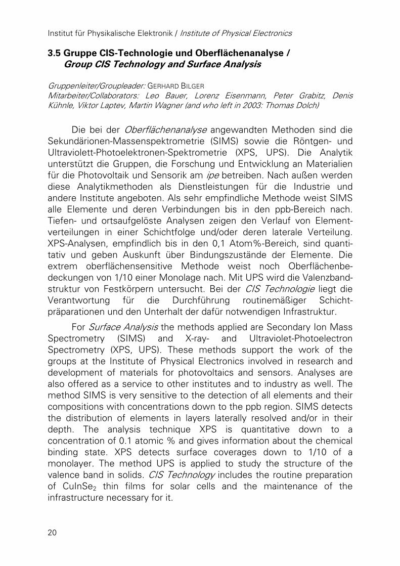
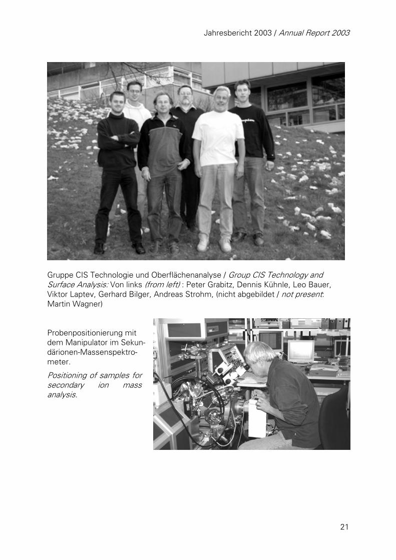
Gruppe CIS Technologie und Oberflächenanalyse / Group CIS Technology and Surface Analysis: Von links (from left) : Peter Grabitz, Dennis Kühnle, Leo Bauer, Viktor Laptev, Gerhard Bilger, Andreas Strohm, (nicht abgebildet / not present: Martin Wagner) Probenpositionierung mit dem Manipulator im Sekun-därionen-Massenspektro-meter.
Positioning of samples for secondary ion mass analysis.
Institut für Physikalische Elektronik / Institute of Physical Electronics
22
3.6 Gruppe Bauelementanalyse / Group Device Analysis Gruppenleiter/Group Leader: UWE RAU Mitarbeiter/Collaborators: Julian Mattheis, Viet Nguyen, Kurt Taretto-Zeyen, Johannes Rostan, Mircea Turcu (and those who left in 2003: Kristin Weinert, Gregor Kron).
Die Gruppe Bauelementanalyse befaßt sich mit der elektrischen und optischen Charakterisierung sowie der numerischen Simulation von Solarzellen basierend auf CdS/Cu(In,Ga)Se2 und a-Si:H/c-Si Heterostrukturen sowie von Farbstoff-Solarzellen auf der Basis von nano-porösem TiO2. Ziel unserer Aktivitäten ist ein grundlegendes Verständnis der Funktionsweise dieser Bauelemente, des Einflusses der Präparationsbedingungen und des Designs des Baulements auf seine Leistungsfähigkeit. Wir benutzen elektrische Analysemethoden wie Strom-Spannungsmessungen, Admittanzspektroskopie und Transienten-Spektroskopie tiefer Störstellen (DLTS). Messungen der internen Quantenausbeute und Photolumineszenz dienen zur Untersuchung der elektro-optischen Eigenschaften der Materialien. Die experimentellen Resultate werden mit quantitativen, numerischen wie analytischen, Modellen verglichen, um ein kohärentes Verständnis der Bauelemente zu erhalten.
The device analysis group is concerned with the electrical and optical characterization and with the numerical simulation of large-area electronic devices such as solar cells based on CdS/Cu(In,Ga)Se2 and a-Si:H/c-Si heterojunctions as well as dye-sensitized solar cells based on nano-porous TiO2. We focus on a fundamental understanding of the working principle of these devices, the influence of preparation conditions and device design on the performance and, finally, on the improvement and optimization. Electrical analysis is performed with the help of current-voltage measurements, admittance spectroscopy, deep level transient spectroscopy (DLTS), and similar methods. Electro-optical analysis comprises measurements of internal quantum efficiency, optical transmittance and reflectance, photoluminescence, etc. The quantitative and coherent interpretation of these experimental results requires detailed modeling and simulation.
Jahresbericht 2003 / Annual Report 2003
23
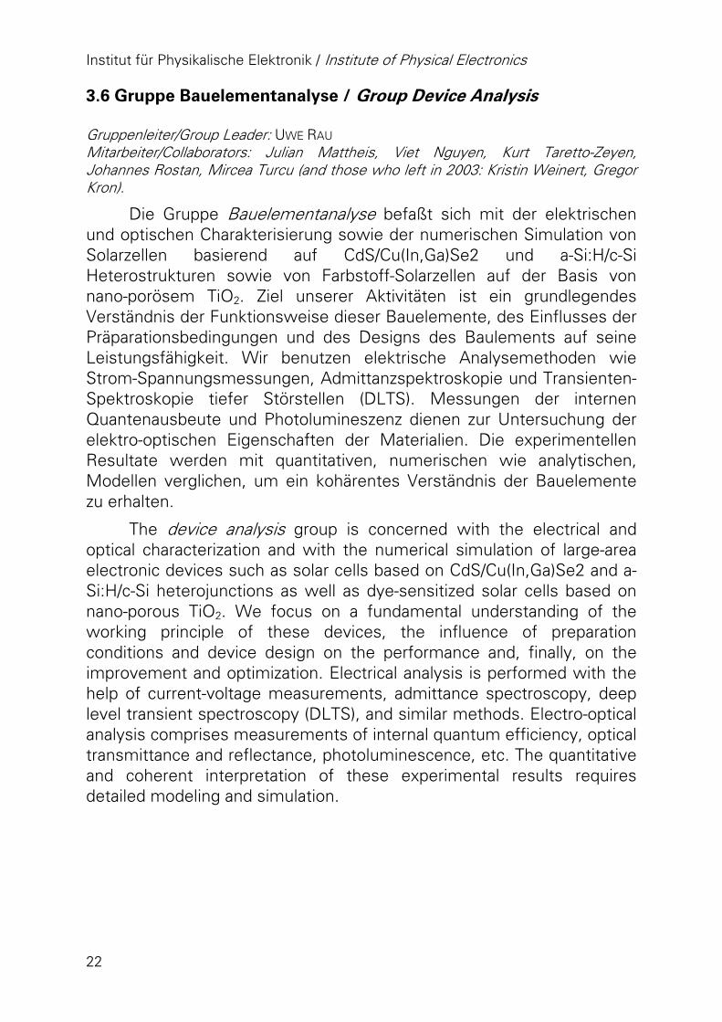
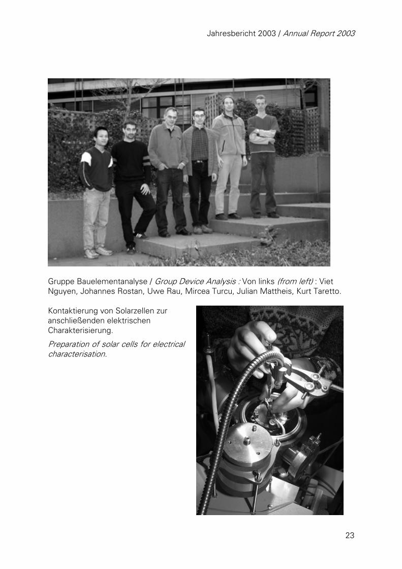
Gruppe Bauelementanalyse / Group Device Analysis : Von links (from left) : Viet Nguyen, Johannes Rostan, Uwe Rau, Mircea Turcu, Julian Mattheis, Kurt Taretto. Kontaktierung von Solarzellen zur anschließenden elektrischen Charakterisierung.
Preparation of solar cells for electrical characterisation.
Institut für Physikalische Elektronik / Institute of Physical Electronics
24
4 Wissenschaftliche Beiträge / Scientific Contributions 4.1 Role of the Cu(In,Ga)Se2 Surface Defect Layer for the
Performance of ZnO/CdS/Cu(In,Ga)(Se,S)2 Solar Cells Author: U. RAU In collaboration with: M. Turcu
The surface properties of Cu(In,Ga)Se2 (CIGS) polycrystalline thin films are especially important as this surface becomes the active interface of the completed ZnO/CdS/CIGS heterojunction solar cells. Especially the question, whether the type inversion of the Cu(In,Ga)Se2 surface defect layer (SDL) of as-grown films [1,2] and of completed heterojunction devices results from an n-type doping of the surface (doping model) or from shallow surface donors that pin the Fermi-level close to the conduction band (pinning model), is still not finally cleared.
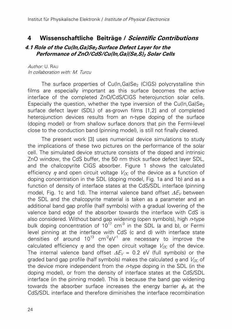
The present work [3] uses numerical device simulations to study the implications of these two pictures on the performance of the solar cell. The simulated device structure consists of the doped and intrinsic ZnO window, the CdS buffer, the 50 nm thick surface defect layer SDL, and the chalcopyrite CIGS absorber. Figure 1 shows the calculated efficiency η and open circuit voltage VOC of the device as a function of doping concentration in the SDL (doping model, Fig. 1a and 1b) and as a function of density of interface states at the CdS/SDL interface (pinning model, Fig. 1c and 1d). The internal valence band offset ∆EV between the SDL and the chalcopyrite material is taken as a parameter and an additional band gap profile (half symbols) with a gradual lowering of the valence band edge of the absorber towards the interface with CdS is also considered. Without band gap widening (open symbols), high n-type bulk doping concentration of 1017 cm-3 in the SDL (a and b), or Fermi level pinning at the interface with CdS (c and d) with interface state densities of around 1013 cm-2eV-1 are necessary to improve the calculated efficiency η and the open circuit voltage VOC of the device. The internal valence band offset ∆EV = 0.2 eV (full symbols) or the graded band gap profile (half symbols) makes the calculated η and VOC of the device more independent from the n-type doping in the SDL (in the doping model), or from the density of interface states at the CdS/SDL interface (in the pinning model). This is because the band gap widening towards the absorber surface increases the energy barrier φb at the CdS/SDL interface and therefore diminishes the interface recombination
Jahresbericht 2003 / Annual Report 2003
25
[4]. The recombination in the space charge region of the absorber becomes thus more prominent, a situation characteristic to devices based on Cu-poor chalcopyrite absorbers. In turn, devices based on absorbers prepared under Cu-rich conditions show relatively low interface barriers and are therefore assumed to be dominated by recombination at the CdS/absorber interface [4,5]. Thus, only such devices without band gap widening need a high n-type doping concentrations in the SDL or Fermi level pinning at the CdS/SDL interface for the minimization of interface recombination. In turn, in high-efficiency Cu-poor devices that posses the SDL with a band gap widening towards the CIGS surface maintain an improved device efficiency and open circuit voltage irrespective of doping concentrations in the SDL or Fermi-level-pinning at the CdS/SDL interface.
12141618
1016 1017
500
600
700
1011 1012 1013
graded
∆EV=0 eV
0.2 eV
(a)
Effic
ienc
y η
[%]
doping conc. [cm-3]
(b)
V OC [m
V]
(c)
interf. st. dens. [cm-2eV-1]
(d)
Figure 1: Calculated efficiency η and open circuit voltage VOC for the n-type SDL (doping model, a and b) and for the SDL with Fermi-level pinning (c and d). An internal valence band offset ∆EV = 0.2 eV (full symbols) or a graded structure (half symbols) makes the parameters, to a first order, independent from the doping concentration in the SDL (within the doping model) or from the density of states at the CdS/SDL interface (within the pinning model). The devices with no internal band offset (open symbols) require high n-type doping or Fermi level pinning.
References:
[1] D. SCHMID, M. RUCKH, F. GRUNWALD, AND H. W. SCHOCK, J. Appl. Phys. 73, 2902 (1993).
[2] M. MORKEL, L. WEINHARDT, B. LOHMÜLLER, C. HESKE, E. UMBACH, W. RIEDL, S. ZWEIGART, AND F. KARG, Appl. Phys. Lett. 79, 4482 (2001).
[3] U. RAU AND M. TURCU, Mat. Res. Soc. Conf. Proc. 763, B8.8 (2003).
[4] M. TURCU AND U. RAU, J. Phys. Chem. Solids 64, 1591 (2003).
[5] M. TURCU, O. PAKMA, AND U. RAU, Appl. Phys. Lett. 80, 2598 (2002).
Institut für Physikalische Elektronik / Institute of Physical Electronics
26
4.2 Efficiency Limitations of Cu(In,Ga)Se2 Solar Cells by Electronic Inhomogeneities
Author: J. H. WERNER In collaboration with: J. Mattheis, U. Rau
World-best solar cells of more than 19 % efficiency and best commercial modules from Cu(In,Ga)Se2 (CIGS) films are fabricated by co-evaporating the constituting elements onto glass substrates. As a result one obtains polycrystalline films of about 2 µm thickness with grain sizes around 0.5 µm. Thus, the films have a high structural disorder due to grain boundaries, dislocations and point defects. In addition, the films are highly compensated and “doped” with Na, O, Cd and other impurities. It is, therefore, evident that such films as well as their interfaces and surfaces must be electronically inhomogeneous. Nevertheless, the modeling of the electronic properties of CIGS solar cells, thus far, has been restricted to models that assume lateral electronic homogeneity.
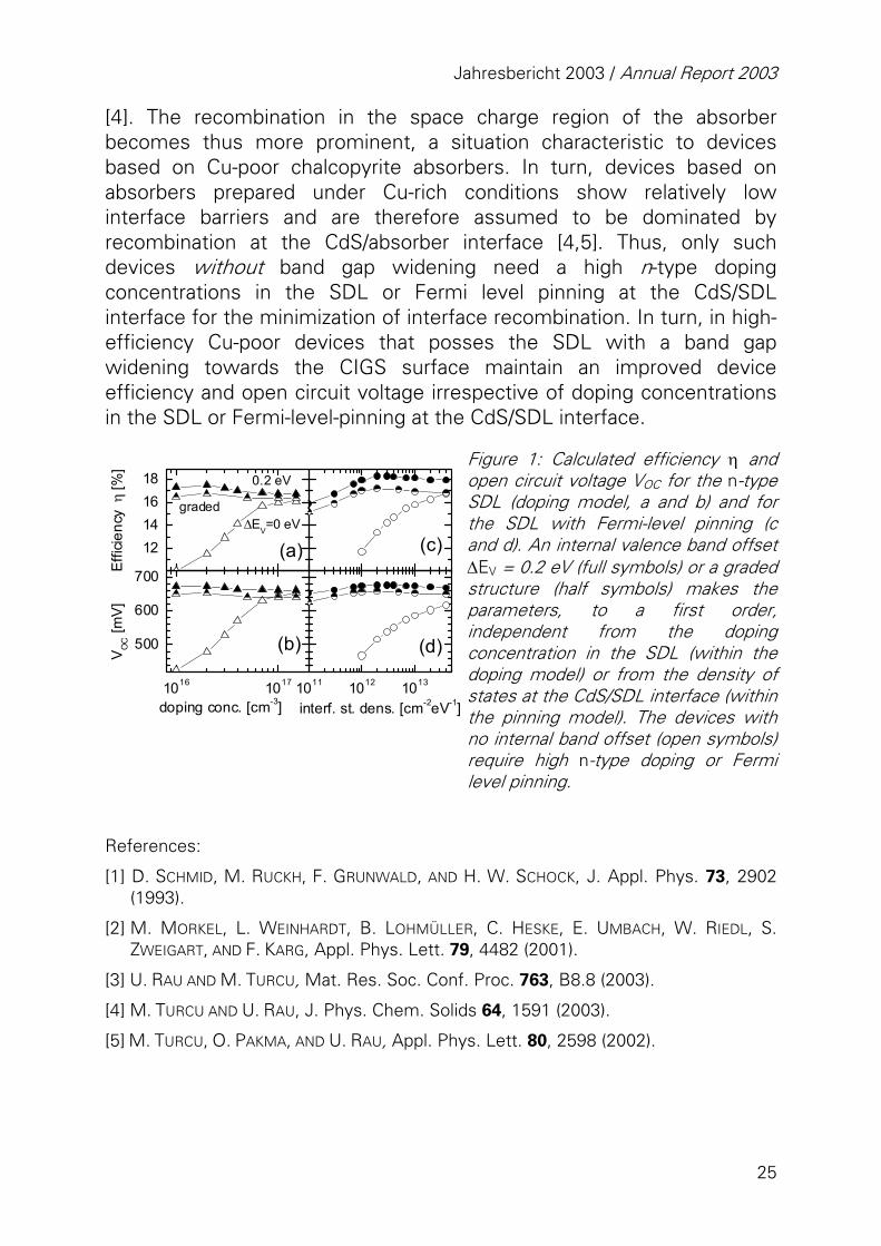
Our research, which is based on earlier models for electronic inhomogeneities at Schottky contacts and silicon grain boundaries [1, 2], showed that the efficiency of the world-best CIGS solar cells is limited by potential fluctuations within the bulk of the polycrystalline CIGS films. Figure 1 shows such potential fluctuations at the conduction and valence band edge. These fluctuations are caused by
i) spatial compositional fluctuations due to variations of the composition, stoichiometry and strain by variations of the Ga/In- and Cu/In-ratio.
ii) electrostatic fluctuations due to the spatial distribution of charges at and within grain boundary planes, dislocations, as well as due to the statistical distribution of bulk defects and of the doping atoms.
Our novel model takes into account both kinds of potential fluctuations [3, 4]. The compositional potential fluctuations are quantified in optical measurements and have a Gaussian standard deviation of 55 meV [3]. If there were only such compositional band gap fluctuations, the present diffusion length of about 3 µm for electrons in CIGS would allow for solar cell efficiencies of about 26 % [4].
Instead of 26 %, the world-best cells reach 18 to19 % efficiency and range thus more than 5 % below the world-best silicon solar cells which
Jahresbericht 2003 / Annual Report 2003
27
make almost 25 %. The reason for the efficiency limitation of CIGS lies in the electrostatic potential fluctuations. Spatially distributed charges at electronic defects give rise to electrostatic fluctuations, resulting in an increased zero bias minority carrier concentration [4]. As a consequence, the saturation current density in the polycrystalline cells is drastically increased and the open circuit voltage is degraded. In addition, electrostatic potential fluctuations cause a diode ideality factor nid > 1. Within our model [4], nid > 1 in the current/voltage curves is a measure for the electronic homogenization of the sample upon the application of either a bias voltage or illumination. From the ideality factor nid = 1.5 we derive Gaussian (zero bias) electrostatic potential fluctuations with a standard deviation of 140 meV. Increasing the efficiency of CIGS cells above 20 % requires a drastic reduction of such electrostatic potential fluctuations.
Figure 1: Potential fluctuations (modelled by Gaussian distributions) in the conduction and valence band result in spatial band gap fluctuations. These band gap fluctuations show up in a lowered efficiency.
References:
[1] J. H. WERNER, Inst. Phys. Conf. Ser. 104, 63 (1989).
[2] J. H. WERNER AND H. H. GÜTTLER, J. Appl. Phys. 69, 1522 (1991); Physica Skripta T39, 258 (1991).
[3] U. RAU AND J. H. WERNER, unpublished.
[4] J. H. WERNER, J. MATTHEIS AND U. RAU, unpublished.
Institut für Physikalische Elektronik / Institute of Physical Electronics
28
4.3 Grain Growth in Thin Cu(In,Ga)Se2 Films Author: T. SCHLENKER In collaboration with: M. Luis Valero, H. W. Schock, J. H. Werner
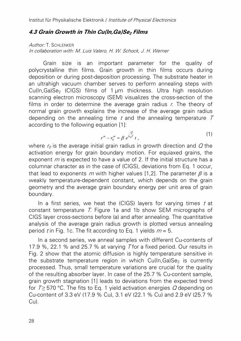
Grain size is an important parameter for the quality of polycrystalline thin films. Grain growth in thin films occurs during deposition or during post-deposition processing. The substrate heater in an ultrahigh vacuum chamber serves to perform annealing steps with Cu(In,Ga)Se2 (CIGS) films of 1 µm thickness. Ultra high resolution scanning electron microscopy (SEM) visualizes the cross-section of the films in order to determine the average grain radius r. The theory of normal grain growth explains the increase of the average grain radius depending on the annealing time t and the annealing temperature T according to the following equation [1]:
(1)
where r0 is the average initial grain radius in growth direction and Q the activation energy for grain boundary motion. For equiaxed grains, the exponent m is expected to have a value of 2. If the initial structure has a columnar character as in the case of (CIGS), deviations from Eq. 1 occur, that lead to exponents m with higher values [1,2]. The parameter β is a weakly temperature-dependent constant, which depends on the grain geometry and the average grain boundary energy per unit area of grain boundary.
In a first series, we heat the (CIGS) layers for varying times t at constant temperature T. Figure 1a and 1b show SEM micrographs of CIGS layer cross-sections before (a) and after annealing. The quantitative analysis of the average grain radius growth is plotted versus annealing period t in Fig. 1c. The fit according to Eq. 1 yields m = 5.
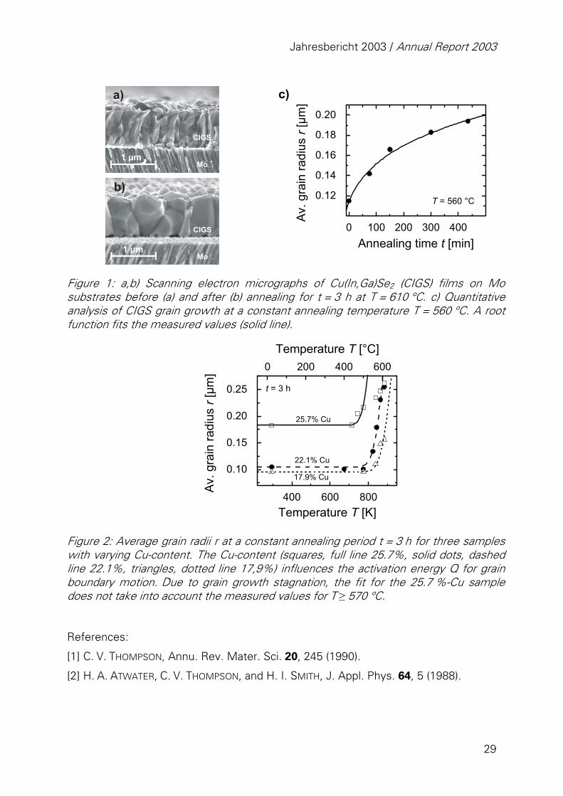
In a second series, we anneal samples with different Cu-contents of 17.9 %, 22.1 % and 25.7 % at varying T for a fixed period. Our results in Fig. 2 show that the atomic diffusion is highly temperature sensitive in the substrate temperature region in which Cu(In,Ga)Se2 is currently processed. Thus, small temperature variations are crucial for the quality of the resulting absorber layer. In case of the 25.7 % Cu-content sample, grain growth stagnation [1] leads to deviations from the expected trend for T ≥ 570 °C. The fits to Eq. 1 yield activation energies Q depending on Cu-content of 3.3 eV (17.9 % Cu), 3.1 eV (22.1 % Cu) and 2.9 eV (25.7 % Cu).
,Bk0 terr T
Qmm
−
=− β
Jahresbericht 2003 / Annual Report 2003
29
400 600 800
0.10
0.15
0.20
0.25 t = 3 h
Temperature T [°C]
Temperature T [K]
Av.
gra
in ra
dius
r [µ
m] 0 200 400 600
17.9% Cu
22.1% Cu
25.7% Cu
Figure 2: Average grain radii r at a constant annealing period t = 3 h for three samples with varying Cu-content. The Cu-content (squares, full line 25.7%, solid dots, dashed line 22.1%, triangles, dotted line 17,9%) influences the activation energy Q for grain boundary motion. Due to grain growth stagnation, the fit for the 25.7 %-Cu sample does not take into account the measured values for T ≥ 570 °C.
References:
[1] C. V. THOMPSON, Annu. Rev. Mater. Sci. 20, 245 (1990).
[2] H. A. ATWATER, C. V. THOMPSON, and H. I. SMITH, J. Appl. Phys. 64, 5 (1988).
1 µm
1 µm
a)
b)
CIGS
Mo
CIGS
Mo
Figure 1: a,b) Scanning electron micrographs of Cu(In,Ga)Se2 (CIGS) films on Mo substrates before (a) and after (b) annealing for t = 3 h at T = 610 °C. c) Quantitative analysis of CIGS grain growth at a constant annealing temperature T = 560 °C. A root function fits the measured values (solid line).
c)
0 100 200 300 400
0.12
0.14
0.16
0.18
0.20
T = 560 °C
Annealing time t [min]
Av.
gra
in ra
dius
r [µ
m]
Institut für Physikalische Elektronik / Institute of Physical Electronics
30
4.4 Influence of Film Texture on Grain Boundary Activity in Cu(In,Ga)Se2 films
Author: G. HANNA In collaboration with: Thilo Glatzel1, S. Sadewasser1, Niels Ott2, H. P. Strunk2, H. W. Schock, U. Rau, J. H. Werner
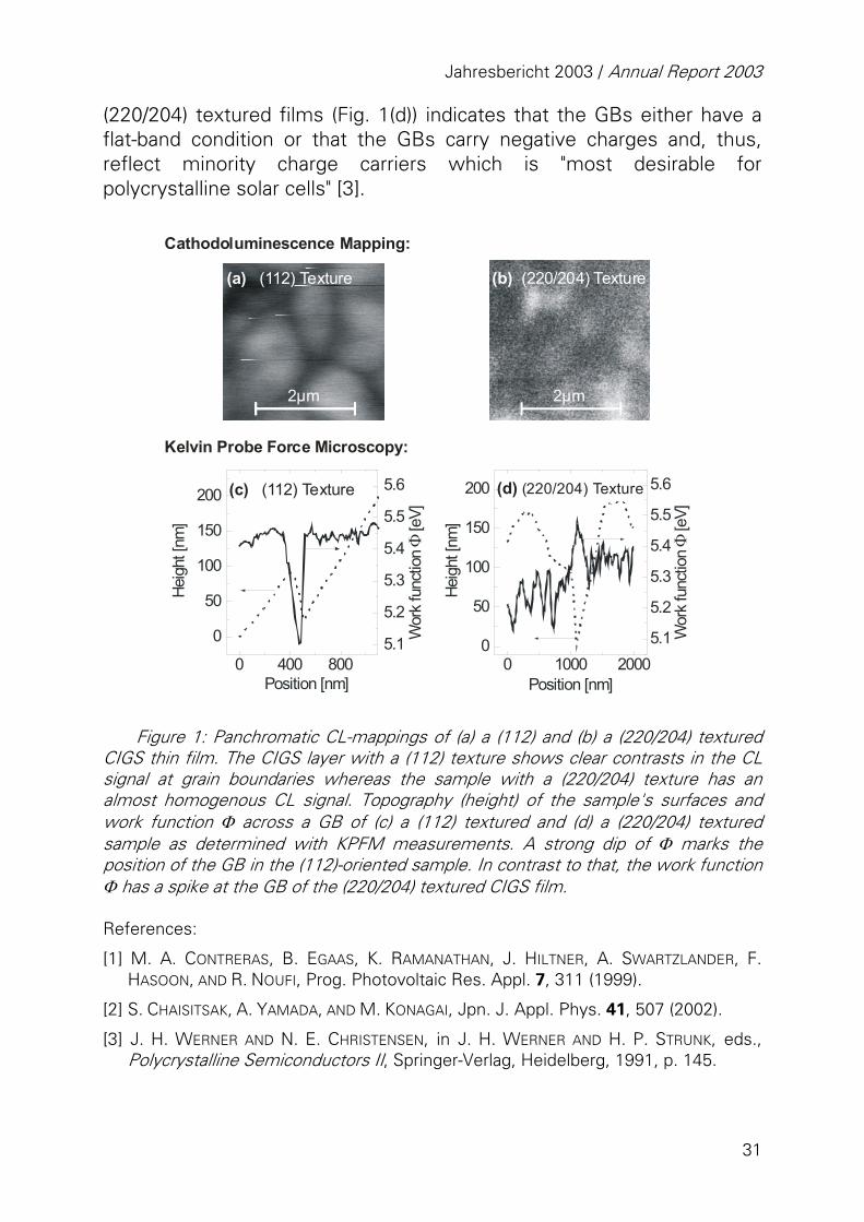
A preferred (220/204) crystallographic orientation (texture) of Cu(In,Ga)Se2 (CIGS) absorber layers most probably is beneficial for the performance of finished CIGS solar cells as compared to (112) textured CIGS layers [1,2]. We study the laterally resolved electronic properties of CIGS thin films with different textures by means of Cathodo-luminescence (CL) mapping, measured in a transmission electron microscope setup, and Kelvin Probe Force Microscopy (KPFM).
Figure 1a, 1b show panchromatic CL-mappings of samples with a (112) and a (220/204) texture. The (220/204) textured sample (Fig. 1b) has a very homogenous lateral CL-intensity whereas the CL mapping of the (112) textured sample (Fig. 1a) exhibits strong contrasts in the CL-signal. Here, the light areas correspond to the grains and the dark areas to the grain boundaries (GBs) of the film. These dark areas indicate an increased non-radiative recombination at the GB of the (112) textured film. Thus, the superior properties of CIGS films with a (220/204) texture as compared to films with a (112) texture are due to a lower electronic activity of the film’s GBs resulting in a lower recombination of minority carriers at the GBs.
The line scans of the work function Φ across GBs in Figs. 1c, 1d yield complementary information about the electronic properties of GBs in (112) or (220/204) textured films. Note, that these scans were measured with KPFM simultaneously with the surface topography. The course of the work function Φ of the (112) textured sample (Fig. 1 (c)) exhibits a dip of more than 300 meV across the GB while at the (220/204) sample (Fig. 1 (d)) Φ shows no comparable dip at the GB but rather has a small spike. The fact that the work function Φ of the (112) textured film (Fig. 1 (c)) is significantly lower at the GB than in the grain indicates that positive charges are present at GBs of such films. Positively charged GBs in polycrystalline p-type semiconductors enhance recombination of charge carriers at GBs and, thus, negatively affect the performance of the finished solar cell [3]. In contrast, the course of Φ of 1 Hahn Meitner Institut, Berlin, Germany 2 Institut für Werkstoffwissenschaften VII, Universität Erlangen-Nürnberg, Germany
Jahresbericht 2003 / Annual Report 2003
31
(220/204) textured films (Fig. 1(d)) indicates that the GBs either have a flat-band condition or that the GBs carry negative charges and, thus, reflect minority charge carriers which is "most desirable for polycrystalline solar cells" [3].
0 400 800
0
50
100
150
200
5.1
5.2
5.3
5.4
5.5
5.6
Heig
ht[n
m]
Position [nm]
Wor
kfu
nctio
nΦ
[eV]
0 1000 20000
50
100
150
200
5.1
5.2
5.3
5.4
5.5
5.6
Heig
ht[n
m]
Position [nm]W
ork
func
tion
Φ[e
V]
2µm
(a) (112) Texture (b) (220/204) Texture
(c) (112) Texture
Kelvin Probe Force Microscopy:
Cathodoluminescence Mapping:
(d) (220/204) Texture
2µm
Figure 1: Panchromatic CL-mappings of (a) a (112) and (b) a (220/204) textured
CIGS thin film. The CIGS layer with a (112) texture shows clear contrasts in the CL signal at grain boundaries whereas the sample with a (220/204) texture has an almost homogenous CL signal. Topography (height) of the sample's surfaces and work function Φ across a GB of (c) a (112) textured and (d) a (220/204) textured sample as determined with KPFM measurements. A strong dip of Φ marks the position of the GB in the (112)-oriented sample. In contrast to that, the work function Φ has a spike at the GB of the (220/204) textured CIGS film. References:
[1] M. A. CONTRERAS, B. EGAAS, K. RAMANATHAN, J. HILTNER, A. SWARTZLANDER, F. HASOON, AND R. NOUFI, Prog. Photovoltaic Res. Appl. 7, 311 (1999).
[2] S. CHAISITSAK, A. YAMADA, AND M. KONAGAI, Jpn. J. Appl. Phys. 41, 507 (2002).
[3] J. H. WERNER AND N. E. CHRISTENSEN, in J. H. WERNER AND H. P. STRUNK, eds., Polycrystalline Semiconductors II, Springer-Verlag, Heidelberg, 1991, p. 145.
Institut für Physikalische Elektronik / Institute of Physical Electronics
32
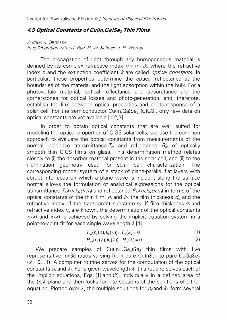
4.5 Optical Constants of Cu(In,Ga)Se2 Thin Films Author: K. ORGASSA In collaboration with: U. Rau, H. W. Schock, J. H. Werner
The propagation of light through any homogeneous material is defined by its complex refractive index ñ = n – ik, where the refractive index n and the extinction coefficient k are called optical constants. In particular, these properties determine the optical reflectance at the boundaries of the material and the light absorption within the bulk. For a photovoltaic material, optical reflectance and absorptance are the cornerstones for optical losses and photo-generation, and, therefore, establish the link between optical properties and photo-response of a solar cell. For the semiconductor Cu(In,Ga)Se2 (CIGS), only few data on optical constants are yet available [1,2,3].
In order to obtain optical constants that are well suited for modeling the optical properties of CIGS solar cells, we use the common approach to evaluate the optical constants from measurements of the normal incidence transmittance Tm and reflectance Rm of optically smooth thin CIGS films on glass. This determination method relates closely to (i) the absorber material present in the solar cell, and (ii) to the illumination geometry used for solar cell characterization. The corresponding model system of a stack of plane-parallel flat layers with abrupt interfaces on which a plane wave is incident along the surface normal allows the formulation of analytical expressions for the optical transmittance Tan(nf,kf,df,ns) and reflectance Ran(nf,kf,df,ns) in terms of the optical constants of the thin film, nf and kf, the film thickness df, and the refractive index of the transparent substrate ns. If film thickness df and refractive index ns are known, the determination of the optical constants nf(λ) and kf(λ) is achieved by solving the implicit equation system in a point-to-point fit for each single wavelength λ [4].
0)())(),(( =− λλλ mffan TknT (1) 0)())(),(( =− λλλ mffan RknR (2)
We prepare samples of Cu(In1-xGax)Se2 thin films with five representative In/Ga ratios varying from pure CuInSe2 to pure CuGaSe2 (x = 0…1). A computer routine serves for the computation of the optical constants nf and kf. For a given wavelength λ, this routine solves each of the implicit equations, Eqs. (1) and (2), individually in a defined area of the (n,k)-plane and then looks for intersections of the solutions of either equation. Plotted over λ, the multiple solutions for nf and kf form several
Jahresbericht 2003 / Annual Report 2003
33
solution branches. The extraction of the true nf and kf dispersion curves necessitates an interpretation of these branches in terms of physical meaningful and implausible solutions. However, owing to the existing knowledge of the optical properties of CIGS (see [2] and references therein), the identification of the correct dispersion curve for nf(λ) - and subsequently for kf(λ) - proves to be unproblematic.
Figure 1 presents the optical constants of Cu(In1-x,Gax)Se2 thin films on glass (solid lines) with relative Ga-contents x as indicated [4]. The error bars for nf and kf indicate the sensitivity of the determination method to the uncertainty ∆df in the input parameter film thickness. The dotted lines present recent data evaluated from bulk material [1,2]. References:
[1] M. I. ALONSO, K. WAKITA, J. PASCUAL, M. GARRIGA, AND N. YAMAMOTO, Phys. Rev. B 63, 075203 (2001)
[2] M. I. ALONSO, M. GARRIGA, C. A. DURANTE RINCÓN, E. HERNÁNDEZ, AND M. LEÓN, Appl. Phys. A 74, 659 (2002).
[3] P. D. PAULSON, R. W. BIRKMIRE, AND W. N. SHAFARMAN, J. Appl. Phys. 94, 879 (2003).
[4] K. ORGASSA, U. RAU, H.-W. SCHOCK, AND J. H. WERNER, to be published in Proc. 3rd World Conf Photovolt. Solar Energy Conversion (Osaka, Japan 2003).
2.5
3.0
3.5
x = 0
refra
ctiv
e in
dex
nf
x = 0
x = 0.2
x = 0.23
x = 0.4
x = 0.51
x = 0.75
x = 0.73
x = 1
x = 1
500 1000 15000.0
0.5
1.0
extin
ctio
n co
effic
ient
kf
500 1000 1500
500 1000 1500
wavelength λ [nm]
500 1000 1500
500 1000 1500
Figure 1: Optical constants of Cu(In1-x,Gax)Se2 with relative Ga-contents x as indicated. Solid lines present thin film data of this contribution [4], dotted lines recent data of bulk material [1,2]. The extinction coefficient kf is significantly lower than that evaluated by spectral ellipsometry of bulk data.
Institut für Physikalische Elektronik / Institute of Physical Electronics
34
4. 6 Qualitative and Quantitative Analysis of Granular CuInSe2 by Electron Beam Induced Current
Author: GERDA C. GLÄSER In collaboration with: U. Rau, H.-W. Schock
Monograin-CuInSe2-solar cells consist of a thick layer of grains embedded in a polymer [1]. The grains with a diameter of about 50µm crystallise from a liquid phase. One of the major problems in measuring and characterising these cells is their heterogeneous nature. Integral measurements are difficult to discuss because of unknown optical and electrical cell properties. Spatially resolving techniques would be most suitable for the investigation of the absorber. One of those techniques is the measurement of electron beam induced currents (EBIC). Micrographs of the EBIC current reveal different response of grains and inhomogeneities within a grain. This is of particular interest because the grains have to be considered as single crystal cells.
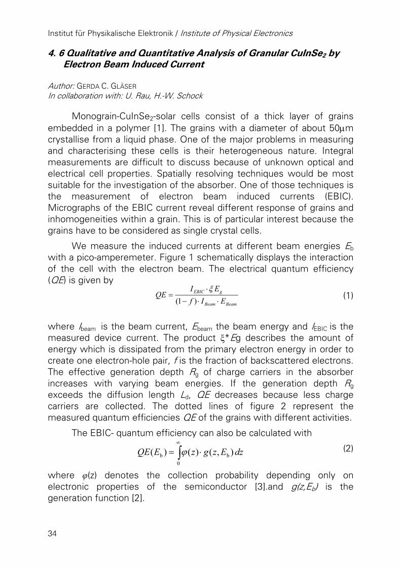
We measure the induced currents at different beam energies Eb with a pico-amperemeter. Figure 1 schematically displays the interaction of the cell with the electron beam. The electrical quantum efficiency (QE) is given by
(1)
where Ibeam is the beam current, Ebeam the beam energy and IEBIC is the measured device current. The product ξ*Eg describes the amount of energy which is dissipated from the primary electron energy in order to create one electron-hole pair, f is the fraction of backscattered electrons. The effective generation depth Rg of charge carriers in the absorber increases with varying beam energies. If the generation depth Rg exceeds the diffusion length Ld, QE decreases because less charge carriers are collected. The dotted lines of figure 2 represent the measured quantum efficiencies QE of the grains with different activities.
The EBIC- quantum efficiency can also be calculated with
(2)
where φ(z) denotes the collection probability depending only on electronic properties of the semiconductor [3].and g(z,Eb) is the generation function [2].
∫∞
⋅=0
bb ),()()( dzEzgzEQE ϕ
BeamBeam
gEBIC
EIfEI
QE⋅⋅−
⋅=
)1(ξ
Jahresbericht 2003 / Annual Report 2003
35
e-
Rgdabs
Ld
window layer
absorber layerEbeam
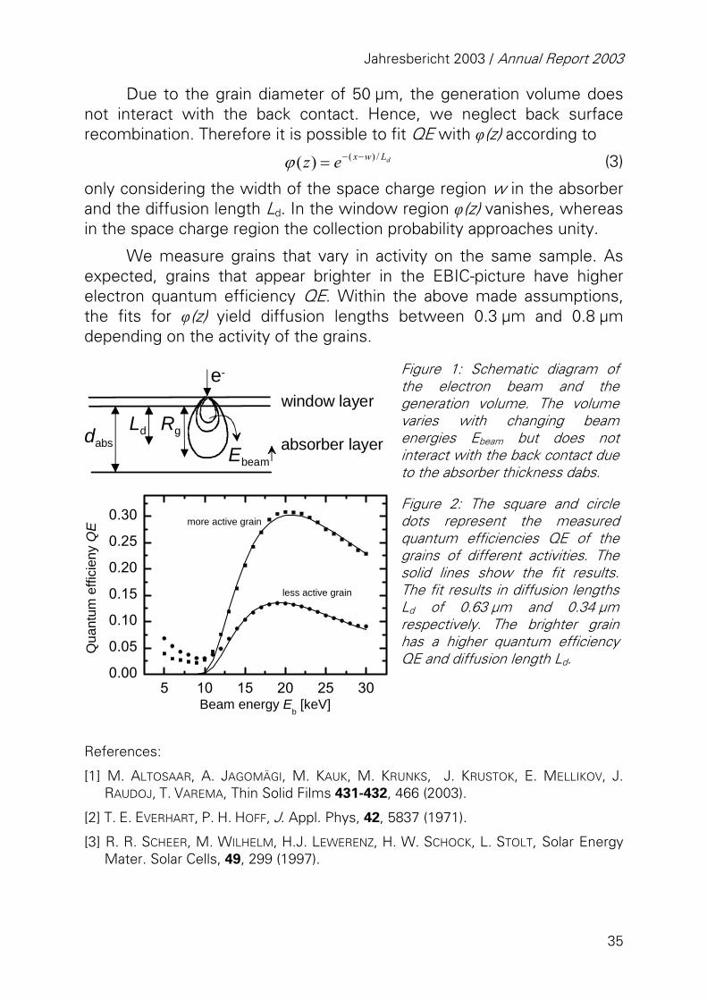
Due to the grain diameter of 50 µm, the generation volume does not interact with the back contact. Hence, we neglect back surface recombination. Therefore it is possible to fit QE with φ(z) according to
(3)
only considering the width of the space charge region w in the absorber and the diffusion length Ld. In the window region φ(z) vanishes, whereas in the space charge region the collection probability approaches unity.
We measure grains that vary in activity on the same sample. As expected, grains that appear brighter in the EBIC-picture have higher electron quantum efficiency QE. Within the above made assumptions, the fits for φ(z) yield diffusion lengths between 0.3 µm and 0.8 µm depending on the activity of the grains.
Figure 1: Schematic diagram of the electron beam and the generation volume. The volume varies with changing beam energies Ebeam but does not interact with the back contact due to the absorber thickness dabs.
Figure 2: The square and circle dots represent the measured quantum efficiencies QE of the grains of different activities. The solid lines show the fit results. The fit results in diffusion lengths Ld of 0.63 µm and 0.34 µm respectively. The brighter grain has a higher quantum efficiency QE and diffusion length Ld.
References:
[1] M. ALTOSAAR, A. JAGOMÄGI, M. KAUK, M. KRUNKS, J. KRUSTOK, E. MELLIKOV, J. RAUDOJ, T. VAREMA, Thin Solid Films 431-432, 466 (2003).
[2] T. E. EVERHART, P. H. HOFF, J. Appl. Phys, 42, 5837 (1971).
[3] R. R. SCHEER, M. WILHELM, H.J. LEWERENZ, H. W. SCHOCK, L. STOLT, Solar Energy Mater. Solar Cells, 49, 299 (1997).
dLwxez /)()( −−=ϕ
5 10 15 20 25 300.00
0.05
0.10
0.15
0.20
0.25
0.30
less active grain
more active grain
Qua
ntum
effi
cien
y Q
E
Beam energy Eb [keV]
Institut für Physikalische Elektronik / Institute of Physical Electronics
36
4.7 Mechanical Properties of Flexible Cu(In,Ga)Se2 Solar Cells Author: P.O. GRABITZ In Collaboration with G. Bilger, S. Enders1
The production of flexible, light-weight solar cells on thin and flexible substrates is one of the future challenges in thin-film solar cell technology. The question is if common solar cell materials, e.g. Cu(In,Ga)Se2 (CIGSe), tolerate the mechanical strain of bending which occurs during preparation and application.
For different bending radii, current voltage (IV)- and quantum efficiency (QE)-measurements were performed. Scanning electron microscope (SEM) and electron beam induced current (EBIC) measurements explain why the efficiencies of convex-bent, i.e. tensile-
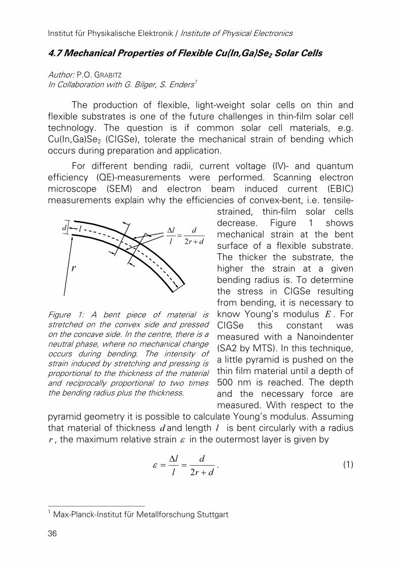
strained, thin-film solar cells decrease. Figure 1 shows mechanical strain at the bent surface of a flexible substrate. The thicker the substrate, the higher the strain at a given bending radius is. To determine the stress in CIGSe resulting from bending, it is necessary to know Young’s modulus E . For CIGSe this constant was measured with a Nanoindenter (SA2 by MTS). In this technique, a little pyramid is pushed on the thin film material until a depth of 500 nm is reached. The depth and the necessary force are measured. With respect to the
pyramid geometry it is possible to calculate Young’s modulus. Assuming that material of thickness d and length l is bent circularly with a radius r , the maximum relative strain ε in the outermost layer is given by
drd
ll
+=
∆=
2ε . (1)
1 Max-Planck-Institut für Metallforschung Stuttgart
drd
ll
+=
∆2
d
r
l
Figure 1: A bent piece of material is stretched on the convex side and pressed on the concave side. In the centre, there is a neutral phase, where no mechanical change occurs during bending. The intensity of strain induced by stretching and pressing is proportional to the thickness of the material and reciprocally proportional to two times the bending radius plus the thickness.
Jahresbericht 2003 / Annual Report 2003
37
The correlation between strain ε and stress σ is given by Hook’s law: σε 1−= E . For the measured IV- and QE-curves it is now possible to
specify stress instead of different bending radii. The experiments yield the following results:
i. Young’s modulus of CIGSe is measured to be 1770 ±=E GPa. This was the first measurement on a CIGSe thin-film material.
ii. In the case of a 5 µm CIGSe layer evaporated on a 200 µm thick metal foil, a bending radius of 25 mm results in %4.0=ε .
iii. Compressive stresses up to 3.0 GPa , which accords to %4.0=ε , cause no significant effects in I/V- and QE-measurements. Further bending causes blistering of the CIGSe layer.
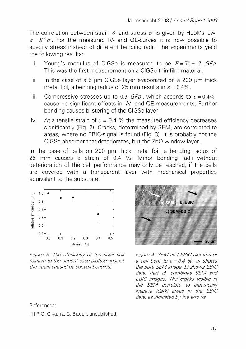
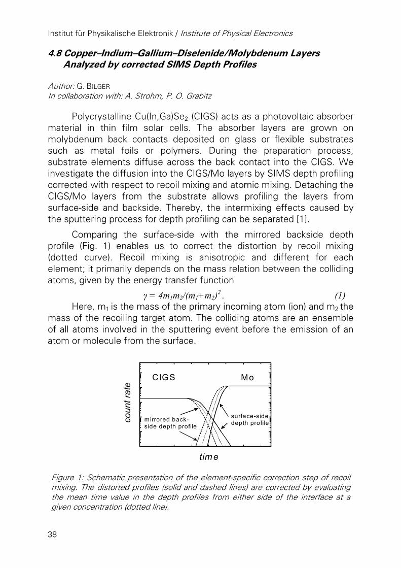
iv. At a tensile strain of ε = 0.4 % the measured efficiency decreases significantly (Fig. 2). Cracks, determined by SEM, are correlated to areas, where no EBIC-signal is found (Fig. 3). It is probably not the CIGSe absorber that deteriorates, but the ZnO window layer.
In the case of cells on 200 µm thick metal foil, a bending radius of 25 mm causes a strain of 0.4 %. Minor bending radii without deterioration of the cell performance may only be reached, if the cells are covered with a transparent layer with mechanical properties equivalent to the substrate.
1.0
0.9
0.8
0.7
0.6
0.5
rel
ativ
e ef
ficie
ncy
η/η
0
0.50.40.30.20.10.0
strain ε [%] 20 µm
a) SEM b) EBIC
c) SEM+EBIC
Figure 3: The efficiency of the solar cell relative to the unbent case plotted against the strain caused by convex bending.
Figure 4: SEM and EBIC pictures of a cell bent to ε = 0.4 %. a) shows the pure SEM image, b) shows EBIC data. Part c), combines SEM and EBIC images. The cracks visible in the SEM correlate to electrically inactive (dark) areas in the EBIC data, as indicated by the arrows
References:
[1] P.O. GRABITZ, G. BILGER, unpublished.
Institut für Physikalische Elektronik / Institute of Physical Electronics
38
4.8 Copper–Indium–Gallium–Diselenide/Molybdenum Layers Analyzed by corrected SIMS Depth Profiles
Author: G. BILGER In collaboration with: A. Strohm, P. O. Grabitz
Polycrystalline Cu(In,Ga)Se2 (CIGS) acts as a photovoltaic absorber material in thin film solar cells. The absorber layers are grown on molybdenum back contacts deposited on glass or flexible substrates such as metal foils or polymers. During the preparation process, substrate elements diffuse across the back contact into the CIGS. We investigate the diffusion into the CIGS/Mo layers by SIMS depth profiling corrected with respect to recoil mixing and atomic mixing. Detaching the CIGS/Mo layers from the substrate allows profiling the layers from surface-side and backside. Thereby, the intermixing effects caused by the sputtering process for depth profiling can be separated [1].
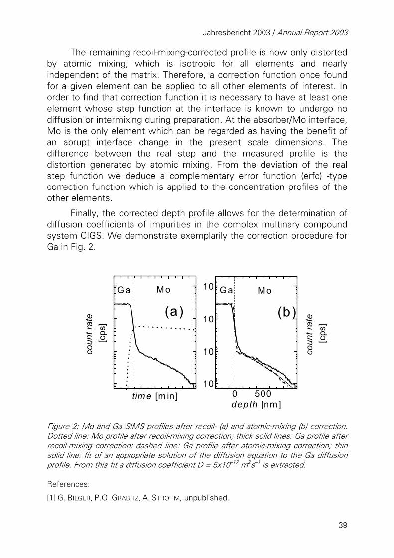
Comparing the surface-side with the mirrored backside depth profile (Fig. 1) enables us to correct the distortion by recoil mixing (dotted curve). Recoil mixing is anisotropic and different for each element; it primarily depends on the mass relation between the colliding atoms, given by the energy transfer function
γ = 4m1m2/(m1+m2)2 . (1) Here, m1 is the mass of the primary incoming atom (ion) and m2 the
mass of the recoiling target atom. The colliding atoms are an ensemble of all atoms involved in the sputtering event before the emission of an atom or molecule from the surface.
coun
t rat
e
time
CIGS Mo
mirrored back- side depth profile
surface-side depth profile
Figure 1: Schematic presentation of the element-specific correction step of recoil mixing. The distorted profiles (solid and dashed lines) are corrected by evaluating the mean time value in the depth profiles from either side of the interface at a given concentration (dotted line).
Jahresbericht 2003 / Annual Report 2003
39
The remaining recoil-mixing-corrected profile is now only distorted by atomic mixing, which is isotropic for all elements and nearly independent of the matrix. Therefore, a correction function once found for a given element can be applied to all other elements of interest. In order to find that correction function it is necessary to have at least one element whose step function at the interface is known to undergo no diffusion or intermixing during preparation. At the absorber/Mo interface, Mo is the only element which can be regarded as having the benefit of an abrupt interface change in the present scale dimensions. The difference between the real step and the measured profile is the distortion generated by atomic mixing. From the deviation of the real step function we deduce a complementary error function (erfc) -type correction function which is applied to the concentration profiles of the other elements.
Finally, the corrected depth profile allows for the determination of diffusion coefficients of impurities in the complex multinary compound system CIGS. We demonstrate exemplarily the correction procedure for Ga in Fig. 2.
104
105
106
107
coun
t rat
e [c
ps]
time [m in]
MoGa
5000
coun
t rat
e [c
ps]
depth [nm]
MoGa
(a) (b)
Figure 2: Mo and Ga SIMS profiles after recoil- (a) and atomic-mixing (b) correction. Dotted line: Mo profile after recoil-mixing correction; thick solid lines: Ga profile after recoil-mixing correction; dashed line: Ga profile after atomic-mixing correction; thin solid line: fit of an appropriate solution of the diffusion equation to the Ga diffusion profile. From this fit a diffusion coefficient D = 5x10–17 m2s–1 is extracted. References:
[1] G. BILGER, P.O. GRABITZ, A. STROHM, unpublished.
Institut für Physikalische Elektronik / Institute of Physical Electronics
40
4.9 Laser-Doping of n+-Type Silicon Solar Cell Emitters Author: A. Esturo-Breton In collaboration with: J. R. Köhler, J. H. Werner
Low-temperature processing of monocrystalline or polycrystalline silicon solar cells has the potential to avoid the production costs of state of the art high-temperature solar cell processing. Such methods do not require expensive equipment and may be competitive, if the throughput can be scaled to a range high enough for in-line processing.
We investigate a pulsed-laser-based doping technique for monocrystalline silicon wafers. Spin-coating of a phosphor-containing doping liquid results in a thin doping layer at the surface of silicon wafers. The focus of a 25 ns pulsed 532 nm frequency doubled Nd:YVO4-laser melts a thin up to 400 nm thick layer of silicon. Phosphor atoms from the doping layer mix with the liquid silicon. Rapid cooling of the melt after the laser pulse induces epitaxial growth of the solidifying phosphorous-doped silicon on the surface of the p-type crystalline silicon wafer.
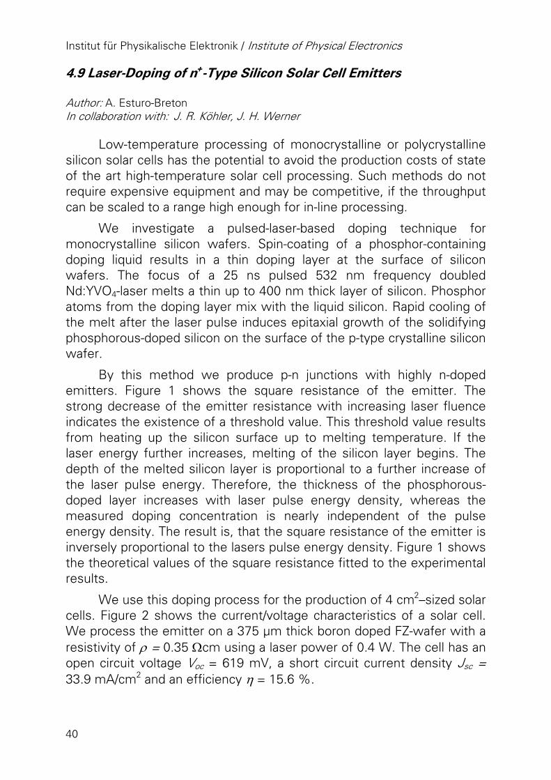
By this method we produce p-n junctions with highly n-doped emitters. Figure 1 shows the square resistance of the emitter. The strong decrease of the emitter resistance with increasing laser fluence indicates the existence of a threshold value. This threshold value results from heating up the silicon surface up to melting temperature. If the laser energy further increases, melting of the silicon layer begins. The depth of the melted silicon layer is proportional to a further increase of the laser pulse energy. Therefore, the thickness of the phosphorous-doped layer increases with laser pulse energy density, whereas the measured doping concentration is nearly independent of the pulse energy density. The result is, that the square resistance of the emitter is inversely proportional to the lasers pulse energy density. Figure 1 shows the theoretical values of the square resistance fitted to the experimental results.
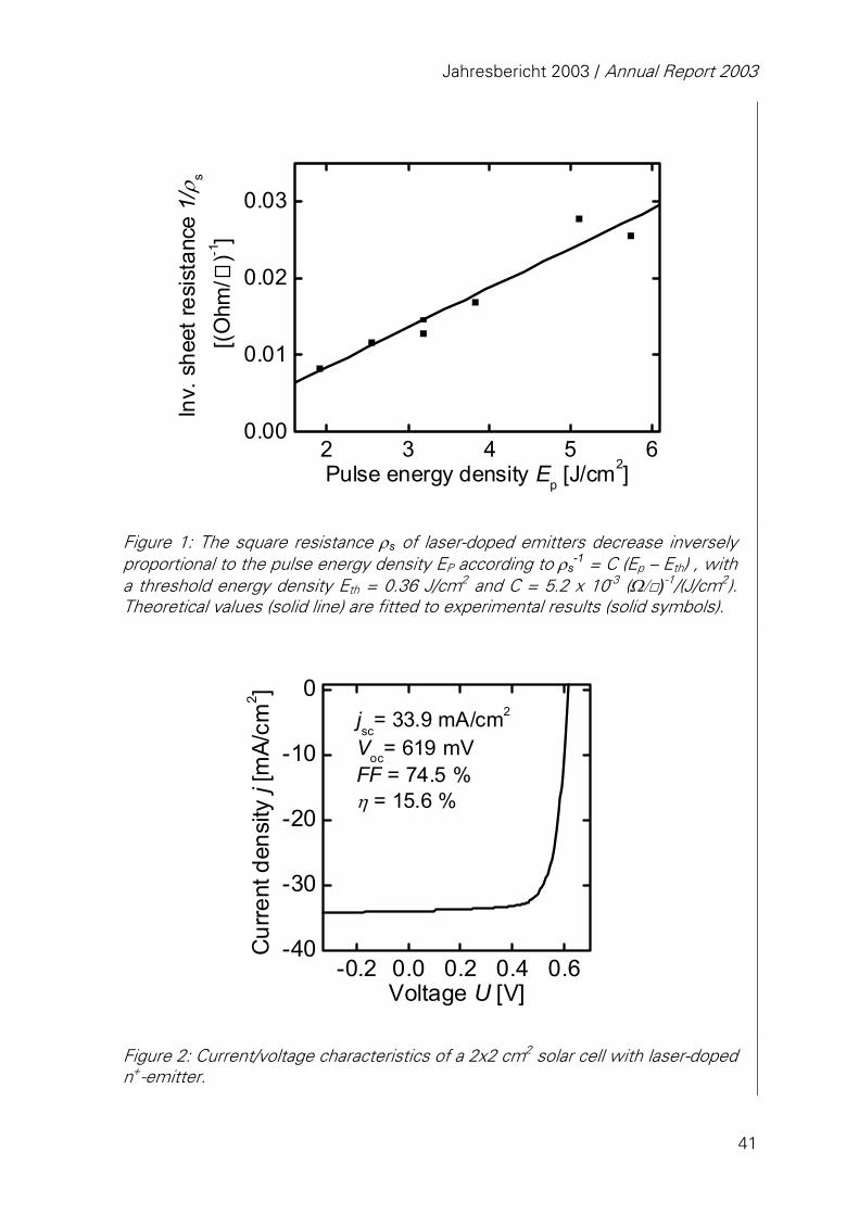
We use this doping process for the production of 4 cm2–sized solar cells. Figure 2 shows the current/voltage characteristics of a solar cell. We process the emitter on a 375 µm thick boron doped FZ-wafer with a resistivity of ρ = 0.35 Ωcm using a laser power of 0.4 W. The cell has an open circuit voltage Voc = 619 mV, a short circuit current density Jsc = 33.9 mA/cm2 and an efficiency η = 15.6 %.
Jahresbericht 2003 / Annual Report 2003
41
2 3 4 5 60.00
0.01
0.02
0.03
Inv.
she
et re
sist
ance
1/ρ
s [(O
hm/
)-1]
Pulse energy density Ep [J/cm2]
Figure 1: The square resistance ρs of laser-doped emitters decrease inversely proportional to the pulse energy density EP according to ρs
-1 = C (Ep – Eth) , with a threshold energy density Eth = 0.36 J/cm2 and C = 5.2 x 10⁻³ (Ω/)-1/(J/cm2). Theoretical values (solid line) are fitted to experimental results (solid symbols).
-0.2 0.0 0.2 0.4 0.6-40
-30
-20
-10
0jsc
= 33.9 mA/cm2
Voc= 619 mVFF = 74.5 %η = 15.6 %
Cur
rent
den
sity
j [m
A/cm
2 ]
Voltage U [V]
Figure 2: Current/voltage characteristics of a 2x2 cm2 solar cell with laser-doped n+-emitter.
Institut für Physikalische Elektronik / Institute of Physical Electronics
42
4.10 Monocrystalline Transfer Silicon with 150 mm Diameter Author: C. BERGE In collaboration with: M. Zhu, M. Schubert, J. H. Werner
The transfer of monocrystalline silicon layers as a way for fabricating thin-film monocrystalline silicon on foreign substrates is one of the key research topics in the silicon group. Last year, we reported the success-ful transfer of such films onto flexible substrates, resulting in a 14.6 % efficient flexible silicon solar cell [1,2], and we still hold the efficiency record for silicon thin-film solar cells [3].
Our transfer process comprises the electrochemical formation of a porous double layer on a silicon substrate, subsequent epitaxial deposition of the silicon device layer on top of the porous substrate surface, device processing by standard wafer technology, and the final transfer of the device layer using the porous layer structure as a “zipper” to detach it from the host wafer.
In 2003, we successfully extended the process from 100 mm wafer technology to 150 mm technology. To enable this upscaling, we developed a new etching system for the formation of the starting porous layer. Figure 1 shows a photograph of this new setup. Apart from the increased substrate size, the system features two more major improvements. The liquid handling is completely automized and microprocessor-controlled, which reduces contamination risk of the etching solution and provides easier handling, and the substrate is fixed inside the system on a vacuum chuck. The latter feature allows complete exposure of the wafer front side to the etching solution, thus the complete front side of the substrate wafer is etched, and enables the transfer of silicon sheets with the complete diameter of 150 mm.
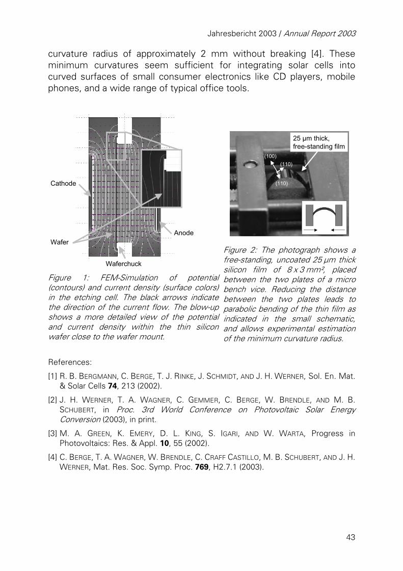
To improve the lateral homogeneity of the porous layers, we performed extensive simulations of the etching current distribution inside the cell using finite element modeling (FEM). Figure 2 shows a calculated two-dimensional potential and current density distribution inside the cell during etching. The numerical simulations correlate well with observations from our experiments and indicate further routes to improve and control the quality of the transfer process.
As one of the aims of our process is the fabrication of flexible solar cells, we investigated the mechanical properties of 25 µm thin silicon sheets that we obtained from our transfer process. Preliminary studies prove that unsupported free standing films can be bent to a minimum
Jahresbericht 2003 / Annual Report 2003
43
curvature radius of approximately 2 mm without breaking [4]. These minimum curvatures seem sufficient for integrating solar cells into curved surfaces of small consumer electronics like CD players, mobile phones, and a wide range of typical office tools.
Figure 1: FEM-Simulation of potential (contours) and current density (surface colors) in the etching cell. The black arrows indicate the direction of the current flow. The blow-up shows a more detailed view of the potential and current density within the thin silicon wafer close to the wafer mount.
25 µm thick, free-standing film
(100)
(110)
(110)
Figure 2: The photograph shows a free-standing, uncoated 25 µm thick silicon film of 8 x 3 mm², placed between the two plates of a micro bench vice. Reducing the distance between the two plates leads to parabolic bending of the thin film as indicated in the small schematic, and allows experimental estimation of the minimum curvature radius.
References:
[1] R. B. BERGMANN, C. BERGE, T. J. RINKE, J. SCHMIDT, AND J. H. WERNER, Sol. En. Mat. & Solar Cells 74, 213 (2002).
[2] J. H. WERNER, T. A. WAGNER, C. GEMMER, C. BERGE, W. BRENDLE, AND M. B. SCHUBERT, in Proc. 3rd World Conference on Photovoltaic Solar Energy Conversion (2003), in print.
[3] M. A. GREEN, K. EMERY, D. L. KING, S. IGARI, AND W. WARTA, Progress in Photovoltaics: Res. & Appl. 10, 55 (2002).
[4] C. BERGE, T. A. WAGNER, W. BRENDLE, C. CRAFF CASTILLO, M. B. SCHUBERT, AND J. H. WERNER, Mat. Res. Soc. Symp. Proc. 769, H2.7.1 (2003).
Anode
Waferchuck
Wafer
Cathode
Institut für Physikalische Elektronik / Institute of Physical Electronics
44
4.11 Recent Developments in Integrated Photovoltaics Author: M. SCHUBERT In collaboration with: C. Gemmer, C. Wagner, J. Krämer, J. H. Werner
Solar cells not only serve for generating electricity at a kW-level on rooftops, but they also enable the mobile use of modern electronic appliances with no need for charging batteries, or carrying heavy and bulky mains-connecting power supplies.
Under the label "integrated photovoltaics - ipv", ipe develops solar cells and small prototype systems for illustrating the potential of such mobile photovoltaic (PV) power supply. One of the prerequisites for such endeavours is to precisely know how much energy the electronic devices (like CD or MP3 players, mobile phones etc.) need, and how much energy they can get from a PV system in practical use. Investigating the performance of different types of solar cells under varying illumination spectra, intensities etc., C. Gemmer gives detailed guidelines for designing ipv systems [1].
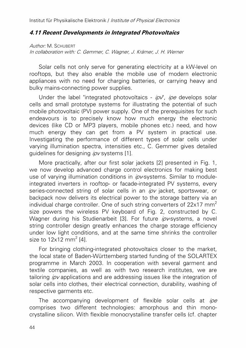
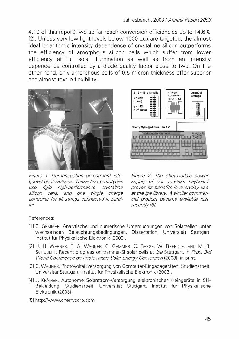
More practically, after our first solar jackets [2] presented in Fig. 1, we now develop advanced charge control electronics for making best use of varying illumination conditions in ipv-systems. Similar to module-integrated inverters in rooftop- or facade-integrated PV systems, every series-connected string of solar cells in an ipv jacket, sportswear, or backpack now delivers its electrical power to the storage battery via an individual charge controller. One of such string converters of 22x17 mm2 size powers the wireless PV keyboard of Fig. 2, constructed by C. Wagner during his Studienarbeit [3]. For future ipv-systems, a novel string controller design greatly enhances the charge storage efficiency under low light conditions, and at the same time shrinks the controller size to 12x12 mm2 [4].
For bringing clothing-integrated photovoltaics closer to the market, the local state of Baden-Württemberg started funding of the SOLARTEX programme in March 2003. In cooperation with several garment and textile companies, as well as with two research institutes, we are tailoring ipv applications and are addressing issues like the integration of solar cells into clothes, their electrical connection, durability, washing of respective garments etc.
The accompanying development of flexible solar cells at ipe comprises two different technologies: amorphous and thin mono-crystalline silicon. With flexible monocrystalline transfer cells (cf. chapter
Jahresbericht 2003 / Annual Report 2003
45
4.10 of this report), we so far reach conversion efficiencies up to 14.6% [2]. Unless very low light levels below 1000 Lux are targeted, the almost ideal logarithmic intensity dependence of crystalline silicon outperforms the efficiency of amorphous silicon cells which suffer from lower efficiency at full solar illumination as well as from an intensity dependence controlled by a diode quality factor close to two. On the other hand, only amorphous cells of 0.5 micron thickness offer superior and almost textile flexibility.
Figure 1: Demonstration of garment inte-grated photovoltaics. These first prototypes use rigid high-performance crystalline silicon cells, and one single charge controller for all strings connected in paral-lel.
Figure 2: The photovoltaic power supply of our wireless keyboard proves its benefits in everyday use at the ipe library. A similar commer-cial product became avaliable just recently [5].
References:
[1] C. GEMMER, Analytische und numerische Untersuchungen von Solarzellen unter wechselnden Beleuchtungsbedingungen, Dissertation, Universität Stuttgart, Institut für Physikalische Elektronik (2003).
[2] J. H. WERNER, T. A. WAGNER, C. GEMMER, C. BERGE, W. BRENDLE, AND M. B. SCHUBERT, Recent progress on transfer-Si solar cells at ipe Stuttgart, in Proc. 3rd World Conference on Photovoltaic Solar Energy Conversion (2003), in print.
[3] C. WAGNER, Photovoltaikversorgung von Computer-Eingabegeräten, Studienarbeit, Universität Stuttgart, Institut für Physikalische Elektronik (2003).
[4] J. KRÄMER, Autonome Solarstrom-Versorgung elektronischer Kleingeräte in Ski-Bekleidung, Studienarbeit, Universität Stuttgart, Institut für Physikalische Elektronik (2003).
[5] http://www.cherrycorp.com
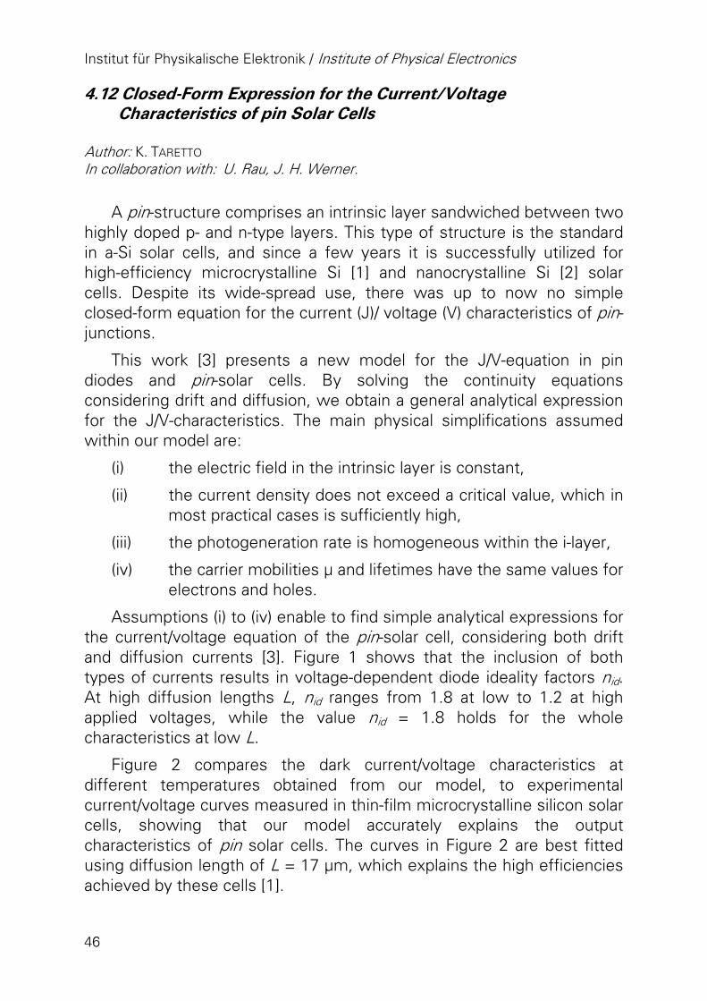
Institut für Physikalische Elektronik / Institute of Physical Electronics
46
4.12 Closed-Form Expression for the Current/Voltage Characteristics of pin Solar Cells
Author: K. TARETTO In collaboration with: U. Rau, J. H. Werner.
A pin-structure comprises an intrinsic layer sandwiched between two highly doped p- and n-type layers. This type of structure is the standard in a-Si solar cells, and since a few years it is successfully utilized for high-efficiency microcrystalline Si [1] and nanocrystalline Si [2] solar cells. Despite its wide-spread use, there was up to now no simple closed-form equation for the current (J)/ voltage (V) characteristics of pin-junctions.
This work [3] presents a new model for the J/V-equation in pin diodes and pin-solar cells. By solving the continuity equations considering drift and diffusion, we obtain a general analytical expression for the J/V-characteristics. The main physical simplifications assumed within our model are:
(i) the electric field in the intrinsic layer is constant,
(ii) the current density does not exceed a critical value, which in most practical cases is sufficiently high,
(iii) the photogeneration rate is homogeneous within the i-layer,
(iv) the carrier mobilities µ and lifetimes have the same values for electrons and holes.
Assumptions (i) to (iv) enable to find simple analytical expressions for the current/voltage equation of the pin-solar cell, considering both drift and diffusion currents [3]. Figure 1 shows that the inclusion of both types of currents results in voltage-dependent diode ideality factors nid. At high diffusion lengths L, nid ranges from 1.8 at low to 1.2 at high applied voltages, while the value nid = 1.8 holds for the whole characteristics at low L.
Figure 2 compares the dark current/voltage characteristics at different temperatures obtained from our model, to experimental current/voltage curves measured in thin-film microcrystalline silicon solar cells, showing that our model accurately explains the output characteristics of pin solar cells. The curves in Figure 2 are best fitted using diffusion length of L = 17 µm, which explains the high efficiencies achieved by these cells [1].
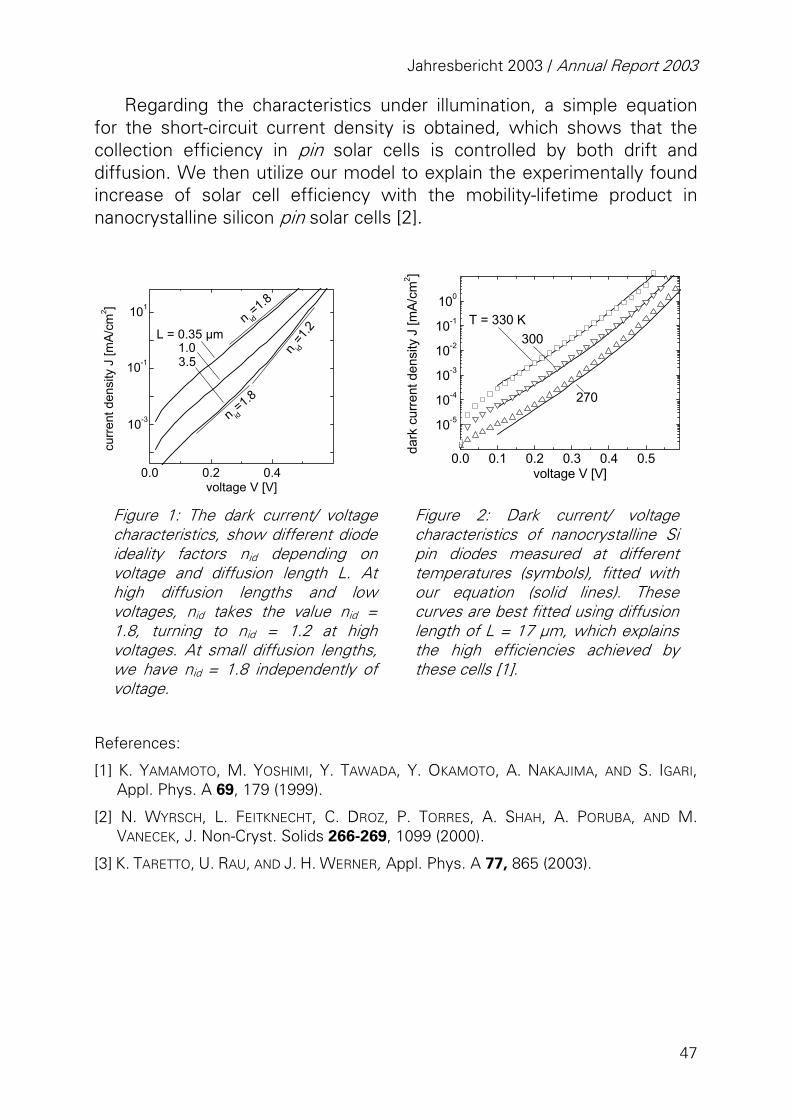
Jahresbericht 2003 / Annual Report 2003
47
Regarding the characteristics under illumination, a simple equation for the short-circuit current density is obtained, which shows that the collection efficiency in pin solar cells is controlled by both drift and diffusion. We then utilize our model to explain the experimentally found increase of solar cell efficiency with the mobility-lifetime product in nanocrystalline silicon pin solar cells [2].
0.0 0.2 0.4
3.5
10-3
10-1
101
n id=1.8
L = 0.35 µmn id
=1.8
1.0 n id=1
.2
curr
ent d
ensi
ty J
[mA
/cm
2 ]
voltage V [V]
0.0 0.1 0.2 0.3 0.4 0.5
10-5
1x10⁻⁴
10-3
1x10⁻²
1x10⁻¹
100
270
300T = 330 K
dark
cur
rent
den
sity
J [m
A/cm
2 ]
voltage V [V]
Figure 1: The dark current/ voltage characteristics, show different diode ideality factors nid depending on voltage and diffusion length L. At high diffusion lengths and low voltages, nid takes the value nid = 1.8, turning to nid = 1.2 at high voltages. At small diffusion lengths, we have nid = 1.8 independently of voltage.
Figure 2: Dark current/ voltage characteristics of nanocrystalline Si pin diodes measured at different temperatures (symbols), fitted with our equation (solid lines). These curves are best fitted using diffusion length of L = 17 µm, which explains the high efficiencies achieved by these cells [1].
References:
[1] K. YAMAMOTO, M. YOSHIMI, Y. TAWADA, Y. OKAMOTO, A. NAKAJIMA, AND S. IGARI, Appl. Phys. A 69, 179 (1999).
[2] N. WYRSCH, L. FEITKNECHT, C. DROZ, P. TORRES, A. SHAH, A. PORUBA, AND M. VANECEK, J. Non-Cryst. Solids 266-269, 1099 (2000).
[3] K. TARETTO, U. RAU, AND J. H. WERNER, Appl. Phys. A 77, 865 (2003).
Institut für Physikalische Elektronik / Institute of Physical Electronics
48
4.13 Influence of the Built-in Voltage on the Fill factor of Dye-Sensitized Solar Cells
Author: G. KRON In collaboration with: M. Duerr1, T. Miteva1, G. Nelles1, A. Yasuda1, K. Taretto, U. Rau, J. H. Werner
Dye-sensitized solar cells (DSSC) [1] are an interesting low-cost alternative to conventional solar cells and, therefore, have attracted considerable interest during the past decade. The basic photovoltaic action of these devices has been studied extensively in the past. After photoexcitation of the dye and ultrafast injection of the excited electrons into the conduction band of the TiO2, the charge carrier transport occurs by diffusion in the nanoporous TiO2 network towards the contacting material. An (equilibrium) built-in voltage Vb
0 evolves close to the interface between the nanoporous TiO2 and the contacting SnO2:F front electrode. However, the importance of this junction potential Vb
0 for the photovoltaic performance of the DSSC is still controversially discussed.
The present work manipulates Vb0 in DSSCs by using different
front contact materials and by investigating the influence of these contact variations on all photovoltaic parameters, i.e., on the complete illuminated current density (J)/voltage (V) characteristics of the devices. By comparing a theoretical model [2] to our experimental results [3], we find that there is no requirement for a charge-separating field in a photovoltaic device, for what concerns the build-up of an open circuit voltage Voc or for a proper charge collection under short circuit conditions. However, a device that is well performing under operation conditions, i.e., that possesses not only Voc and a short circuit current Jsc but also a reasonable fill factor FF, clearly requires a built-in field.
For the preparation of the DSSCs under investigation, we use glass substrates covered with four different conducting materials: the standard SnO2:F as well as Al, Au, and ZnO:Al. The range of work function embraced by these materials stretches from Ew (Al) ≈ 4.3 eV to Ew (Au) ≈ 5.1 eV. Figure 1 shows the measured J/V-characteristics of the four devices under illumination through the semi-transparent Pt-back electrode. Whereas the standard SnO2:F contact yields the best efficiency, mainly because of the high fill factor, the front contact materials with higher Ew and, therefore, lower Vbi
0, i.e. ZnO and Au, lead to a degenerate, S-shaped J/V-characteristics. While we observe huge
1 Sony International (Europe) GmbH, MSL, Stuttgart, Germany
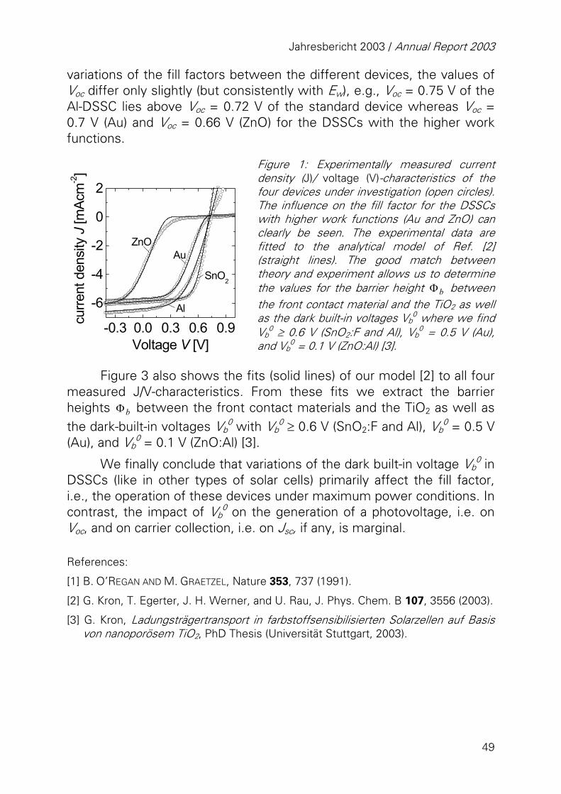
Jahresbericht 2003 / Annual Report 2003
49
variations of the fill factors between the different devices, the values of Voc differ only slightly (but consistently with Ew), e.g., Voc = 0.75 V of the Al-DSSC lies above Voc = 0.72 V of the standard device whereas Voc = 0.7 V (Au) and Voc = 0.66 V (ZnO) for the DSSCs with the higher work functions.
-0.3 0.0 0.3 0.6 0.9
-6
-4
-2
0
2
SnO2
Al
ZnOAu
curre
nt d
ensi
ty J
[mAc
m-2]
Voltage V [V]
Figure 1: Experimentally measured current density (J)/ voltage (V)-characteristics of the four devices under investigation (open circles). The influence on the fill factor for the DSSCs with higher work functions (Au and ZnO) can clearly be seen. The experimental data are fitted to the analytical model of Ref. [2] (straight lines). The good match between theory and experiment allows us to determine the values for the barrier height bΦ between the front contact material and the TiO2 as well as the dark built-in voltages Vb
0 where we find Vb
0 ≥ 0.6 V (SnO2:F and Al), Vb0 = 0.5 V (Au),
and Vb0 = 0.1 V (ZnO:Al) [3].
Figure 3 also shows the fits (solid lines) of our model [2] to all four measured J/V-characteristics. From these fits we extract the barrier heights bΦ between the front contact materials and the TiO2 as well as the dark-built-in voltages Vb
0 with Vb0 ≥ 0.6 V (SnO2:F and Al), Vb
0 = 0.5 V (Au), and Vb
0 = 0.1 V (ZnO:Al) [3].
We finally conclude that variations of the dark built-in voltage Vb0 in
DSSCs (like in other types of solar cells) primarily affect the fill factor, i.e., the operation of these devices under maximum power conditions. In contrast, the impact of Vb
0 on the generation of a photovoltage, i.e. on Voc, and on carrier collection, i.e. on Jsc, if any, is marginal. References:
[1] B. O’REGAN AND M. GRAETZEL, Nature 353, 737 (1991).
[2] G. Kron, T. Egerter, J. H. Werner, and U. Rau, J. Phys. Chem. B 107, 3556 (2003).
[3] G. Kron, Ladungsträgertransport in farbstoffsensibilisierten Solarzellen auf Basis von nanoporösem TiO2, PhD Thesis (Universität Stuttgart, 2003).
Institut für Physikalische Elektronik / Institute of Physical Electronics
50
5. Verzeichnis der Publikationen/ List of Publications (erschienen 11/2002 bis 10/2003 / published 11/2002 to 10/2003)
1 C. BERGE, T. A. WAGNER, W. BRENDLE, C. CRAFF-CASTILLO, M. B. SCHUBERT, AND J. H. WERNER, Flexible Monocrystalline Si Films for Thin Film Devices from Transfer Processes, Mat. Res. Soc. Symp. Proc. 769, H2.7 (2003).
2 G. HANNA, J. MATTHEIS, V. Laptev, Y. Yamamoto, U. Rau, and H. W. Schock, Influence of the Selenium Flux on the Growth Cu(In,Ga)Se2 Thin Films, Thin Solid Films 431-432, 31 (2003).
3 M. IGALSON, M. BODEGARD, L. STOLT, AND A. JASENEK, The 'Defected Layer' and the Mechanism of the Interface-Related Metastable Behavior in the ZnO/CdS/Cu(In,Ga)Se2 Devices, Thin Solid Films 431-432, 153 (2003).
4 A. JASENEK, U. RAU, K. WEINERT, H. W. SCHOCK, AND J. H. WERNER, Illumination-Enhanced Annealing of Electron Irradiated Cu(In,Ga)Se2 Solar Cells, in Proc. 29th IEEE Photov. Spec. Conf. (IEEE, New York, 2002) p. 872.
5 A. JASENEK, U. RAU, K. WEINERT, H. W. SCHOCK, AND J. H. WERNER, Illumination-Induced Recovery of Cu(In,Ga)Se2 Solar Cells after High-Energy Electron Irradiation, Appl. Phys. Lett. 82, 1410 (2003).
6 R. KNIESE, D. HARISKOS, G. VOORWINDEN, U. RAU, AND M. POWALLA, High Band Gap Cu(In,Ga)Se2 Solar Cells and Modules Fabricated with in-line Co-evaporation, Thin Solid Films 431-432, 543 (2003).
7 I. M. KÖTSCHAU, G. BILGER, AND H. W. SCHOCK, Depth Profiling of Cu(In,Ga)Se2 by Grazing Incidence X-ray Diffraction, Mat. Res. Soc. Conf. Proc. 763, B6.2 (2003).
8 I. M. KÖTSCHAU AND H. W. SCHOCK, Depth profile of the lattice constant of the Cu-poor surface layer in (Cu2Se)1-x(In2Se3)x evidenced by grazing incidence X-ray diffraction, J. Phys. Chem. Solids 64, 1559 (2003).
9 G. KRON, U. RAU, M. DÜRR, T. MITEVA, G. NELLES, A. YASUDA, AND J. H. WERNER, Diffusion Limitations to I3− /I− Electrolyte Transport through Nanoporous TiO2 Networks, Electrochem. Solid-State Lett. 6, E11 (2003).
10 G. KRON, T. EGERTER, J. H. WERNER, AND U. RAU, Electronic Transport in Dye Sensitized Nanocrystalline TiO2 Solar Cells – Comparison of Electrolyte and Solid-State Devices, J. Phys. Chem. B 107, 3556 (2003).
11 G. KRON, U. RAU, AND J. H. WERNER, Influence of the built-in voltage on the fill factor of dye sensitized solar cells, J. Phys. Chem. B 107, 13258 (2003).
12 M. NERDING, S. CHRISTIANSEN, R. DASSSOW, K. TARETTO, J. R. KOEHLER, AND
H. P. STRUNK, Tailoring Texture in Laser Crystallization of Silicon Thin-Films on Glass, Solid State Phenomena 93, 173 (2003).
Jahresbericht 2003 / Annual Report 2003
51
13 Q. NGUYEN, K. ORGASSA, I. M. KÖTSCHAU, U. RAU, AND H. W. SCHOCK, Influence of Heterointerfaces on the Performance of Cu(In,Ga)Se2 Solar Cells with CdS and In(OHxS y) Buffer Layers, Thin Solid Films 431-432, 330 (2003).
14 Q. NGUYEN, G. BILGER, U. RAU, AND H. W. SCHOCK, Modification of Cu(In,Ga)Se2 Surface by Treatment in Cadmium Solutions, Mat. Res. Soc. Conf. Proc. 763, B8.17 (2003).
15 K. ORGASSA, H. W. SCHOCK, AND J. H. WERNER, Alternative Back Contact Materials for Thin Film Cu(In,Ga)Se2 Solar Cells, Thin Solid Films 431-432, 387 (2003).
16 N. OTT, G. HANNA, M. ALBRECHT, U. RAU, J. H. WERNER, AND H. P. STRUNK, Cathodoluminescence Studies of Cu(In,Ga)Se2 Thin-Films, Solid State Phenomena 93, 133 (2003).
17 F. PFISTERER, The Wet-Topotaxial Process of Junction Formation and Surface Treatments of Cu2S-CdS Thin-Film Solar Cells, Thin Solid Films 431-432, 470 (2003).
18 U. RAU AND M. TURCU, Role of Surface Band-gap Widening in Cu(In,Ga)(Se,S)2 Thin-Films for the Photovoltaic Performance of ZnO/CdS/Cu(In,Ga)(Se,S)2 Heterojunction Solar Cells, Mat. Res. Soc. Conf. Proc. 763, B8.8 (2003).
19 U. RAU, G. KRON, AND J. H. WERNER, Reply to Comments on “Electronic Transport in Dye-Sensitized Nanoporous TiO2 Solar Cells - Comparison of Electrolyte and Solid-State Devices”: On the Photovoltaic Action in pn-Junction and Dye-Sensitized Solar Cells, J. Phys. Chem. B 107 13547 (2003).
20 B. SCHATTAT, W. BOLSE, S. KLAUMUNZER, F. HARBSMEIER, AND A. JASENEK, Atomic Mixing of Ni2O3/SiO2, NiO/SiO2, and Ni/SiO2 Interfaces Induced by Swift Heavy Ion Irradiation, Appl. Phys. A 76, 165 (2003).
21 B. SCHATTAT, W. BOLSE, S. KLAUMUNZER, F. HARBSMEIER, AND A. JASENEK, Interface Mixing of CuOx/SiO2 Bilayers by Swift Heavy Ions, Nucl. Instrum. Meth. B 191, 577 (2002).
22 T. SCHLENKER, H. W. SCHOCK, AND J. H. WERNER, Initial Growth Behavior of Cu(In,Ga)Se2 on Molybdenum Substrates, J. Cryst. Growth 259, 47
(2003).
23 T. SCHLENKER, K. ORGASSA, H. W. SCHOCK, AND J. H. WERNER, Nucleation of Cu(In,Ga)Se2 on Molybdenum Substrates, Mat. Res. Soc. Conf. Proc. 763, B8.7 (2003).
24 H. W. SCHOCK, Material Related Prerequisites for Chalcopyrite Based Thin Film Solar Cells, Mat. Res. Soc. Conf. Proc. 763, B1.6 (2003).
25 K. TARETTO, U. RAU, AND J. H. WERNER, Closed-Form Expression for the Current/Voltage Characteristics of pin Solar Cells, Appl. Phys. A 77, 865 (2003).
Institut für Physikalische Elektronik / Institute of Physical Electronics
52
26 K. TARETTO, U. RAU, AND J. H. WERNER, Method to Extract the Diffusion Length from Solar Cell Parameters – Application to Polycrystalline Silicon, J. Appl. Phys. 93, 5447 (2003).
27 K. TARETTO, U. RAU, T. A. WAGNER, AND J. H. WERNER, A Simple Method to Extract the Diffusion Length from the Output Parameters of Solar Cells – Application to Polycrystalline Silicon, Solid State Phenomena 93, 399
(2003).
28 M. TURCU AND U. RAU, Fermi Level Pinning at CdS/Cu(In,Ga)(Se,S)2 Interfaces: Effect of Chalcopyrite Alloy Composition, J. Phys. Chem. Solids 64, 1591 (2003).
29 M. TURCU AND U. RAU, Compositional Trends of Defect Energies, Band Alignments, and Recombination Mechanisms in the Cu(In,Ga)(Se,S)2 Alloy System, Thin Solid Films 431-432, 158 (2003).
30 T. A. WAGNER AND U. RAU, Temperature Dependent Quantum Efficiency Measurements for the Analysis of Recombination Centers in Epitaxial Silicon Thin-Film Solar Cells, Appl. Phys. Lett. 82, 2637 (2003).
31 T. A. WAGNER, L. OBERBECK, R. B. BERGMANN, M. NERDING, H. P. STRUNK, AND J. H. WERNER, Low-Temperature Epitaxy on Polycrystalline Silicon Substrates, Solid State Phenomena 93, 121 (2003).
32 K. WEINERT, A. JASENEK, AND U. RAU, Consequence of 3-MeV Electron Irradiation on the Photovoltaic Output Parameters of Cu(In,Ga)Se2 Solar Cells, Thin Solid Films 431-432, 453 (2003).
Jahresbericht 2003 / Annual Report 2003
53
6 Promotionen 2003 / Ph. D. Theses 2003
GEMMER, CHRISTIAN Analytische und numerische Untersuchungen von Solarzellen unter wechselnden Beleuchtungsbedingungen
KÖTSCHAU, IMMO Strukturelle Eigenschaften von Cu(In,Ga)(Se,S)2-Dünnschichten
KRON, GREGOR Ladungsträgertransport in farbstoffsensibilisierten Solarzellen auf Basis von nanoporösem TiO2
RINKE, TITUS Transfersolarzellen aus monokristallinem Dünnschichtsilicium
ROJAHN, MARTIN Encapsulation of a retina implant
TARETTO, KURT Modelling and characterization of polycrystalline silicon for solar cells and microelectronics
WAGNER, THOMAS Low temperature silicon epitaxy – defects and electronic properties
WEINERT, KRISTIN Einfluss von Protonen- und Elektronenbestrahlungen auf die photovoltaischen Parameter von Cu(In,Ga)Se2-Solarzellen
Nachtrag / Addendum
DULLWEBER, THORSTEN Optimierung des Wirkungsgrades von Cu(In,Ga)Se2-Solarzellen mittels variablem Verlauf der Bandlücke, 2002
JENSEN, NILS Heterostruktursolarzellen aus amorphem und kristallinem Silicum, 2002
Institut für Physikalische Elektronik / Institute of Physical Electronics
54
7 Diplomarbeiten 2003 / Diploma Thesis Projects 2003
BOZSA, ANDREAS Nanokristalline Si-Solarzellen aus gepulster Gasphasenabscheidung
ESTURO-BRETÓN, AINHOA Emitterdiffusion für Silicium-Solarzellen mittels Laserannealing
LUÍS, MARTA Einfluss der Nukleationsphase auf das Wachstum dünner Cu(In,Ga)Se2–Schichten
NYANOD, NDONGWA Aufnahme und Wiedergabe großformatiger Bilder
ROSTAN, JOHANNES Sammlungseigenschaften von Cu(In,Ga)Se2 - Solarzellen mit transparenten Rückkontakten
SCHLEUßNER, SEBASTIAN Optical trapping for CIGS thin film solar cells–Preparation and characterization of test devices
SPEER, TIM Wechselrichter für Photovoltaik-Systeme
Jahresbericht 2003 / Annual Report 2003
55
8 Studienarbeiten 2003 / Major Term Projects 2003
BOGICEVIC, MARTIN Ortsaufgelöste Charakterisierung von Monograin-Solarzellen
BOZSA, ANDREAS Inbetriebnahme eines automatischen Inspektionsplatzes und die Erstellung von Inspektionsstrategien
GAUGLER, ELMAR Entwurf von Power-on Reset Schaltungen für die neue 0.5 µm CMOS Mixed-Signal Gate Array Umgebung am IMS
KERN, ALBRECHT Messung der zeitlichen Helligkeitsverteilung einer Versuchs-OLED
MADER, DENIS Quasi-epitaktisches Wachstum von Cu(In,Ga)Se2 – Schichten auf laserkristallisierten Saatschichten
STAACK, JOCHEN Untersuchung optischer Eigenschaften farbstoffsensibilisierter Solarzellen
WAGNER, CHRISTOF Photovoltaik-Versorgung von Computer-Eingabegeräten
WERNER, JÖRG Programmierung einer grafischen Bedienoberfläche für die Steuerung einer Vakuum-Beschichtungsanlage mit Visual Basic
ZINßER, BASTIAN Solare Stromerzeugung auf Zypern – Erfassen und Aufbereiten von Daten
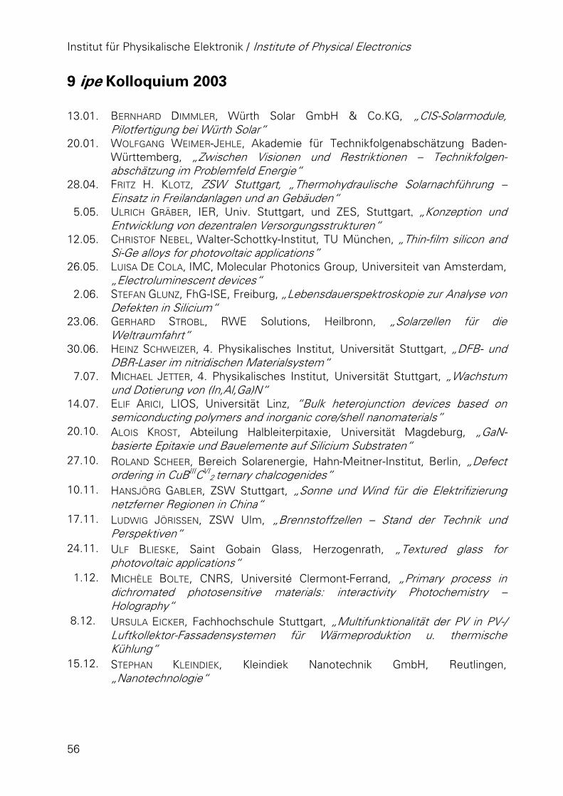
Institut für Physikalische Elektronik / Institute of Physical Electronics
56
9 ipe Kolloquium 2003 13.01. BERNHARD DIMMLER, Würth Solar GmbH & Co.KG, „CIS-Solarmodule,
Pilotfertigung bei Würth Solar“ 20.01. WOLFGANG WEIMER-JEHLE, Akademie für Technikfolgenabschätzung Baden-
Württemberg, „Zwischen Visionen und Restriktionen – Technikfolgen-abschätzung im Problemfeld Energie“
28.04. FRITZ H. KLOTZ, ZSW Stuttgart, „Thermohydraulische Solarnachführung – Einsatz in Freilandanlagen und an Gebäuden“
5.05. ULRICH GRÄBER, IER, Univ. Stuttgart, und ZES, Stuttgart, „Konzeption und Entwicklung von dezentralen Versorgungsstrukturen“
12.05. CHRISTOF NEBEL, Walter-Schottky-Institut, TU München, „Thin-film silicon and Si-Ge alloys for photovoltaic applications”
26.05. LUISA DE COLA, IMC, Molecular Photonics Group, Universiteit van Amsterdam, „Electroluminescent devices“
2.06. STEFAN GLUNZ, FhG-ISE, Freiburg, „Lebensdauerspektroskopie zur Analyse von Defekten in Silicium“
23.06. GERHARD STROBL, RWE Solutions, Heilbronn, „Solarzellen für die Weltraumfahrt“
30.06. HEINZ SCHWEIZER, 4. Physikalisches Institut, Universität Stuttgart, „DFB- und DBR-Laser im nitridischen Materialsystem“
7.07. MICHAEL JETTER, 4. Physikalisches Institut, Universität Stuttgart, „Wachstum und Dotierung von (In,Al,Ga)N“
14.07. ELIF ARICI, LIOS, Universität Linz, “Bulk heterojunction devices based on semiconducting polymers and inorganic core/shell nanomaterials”
20.10. ALOIS KROST, Abteilung Halbleiterpitaxie, Universität Magdeburg, „GaN-basierte Epitaxie und Bauelemente auf Silicium Substraten“
27.10. ROLAND SCHEER, Bereich Solarenergie, Hahn-Meitner-Institut, Berlin, „Defect ordering in CuBIIICVI
2 ternary chalcogenides” 10.11. HANSJÖRG GABLER, ZSW Stuttgart, „Sonne und Wind für die Elektrifizierung
netzferner Regionen in China“ 17.11. LUDWIG JÖRISSEN, ZSW Ulm, „Brennstoffzellen – Stand der Technik und
Perspektiven“ 24.11. ULF BLIESKE, Saint Gobain Glass, Herzogenrath, „Textured glass for
photovoltaic applications“ 1.12. MICHÈLE BOLTE, CNRS, Université Clermont-Ferrand, „Primary process in
dichromated photosensitive materials: interactivity Photochemistry – Holography“
8.12. URSULA EICKER, Fachhochschule Stuttgart, „Multifunktionalität der PV in PV-/ Luftkollektor-Fassadensystemen für Wärmeproduktion u. thermische Kühlung“
15.12. STEPHAN KLEINDIEK, Kleindiek Nanotechnik GmbH, Reutlingen, „Nanotechnologie“
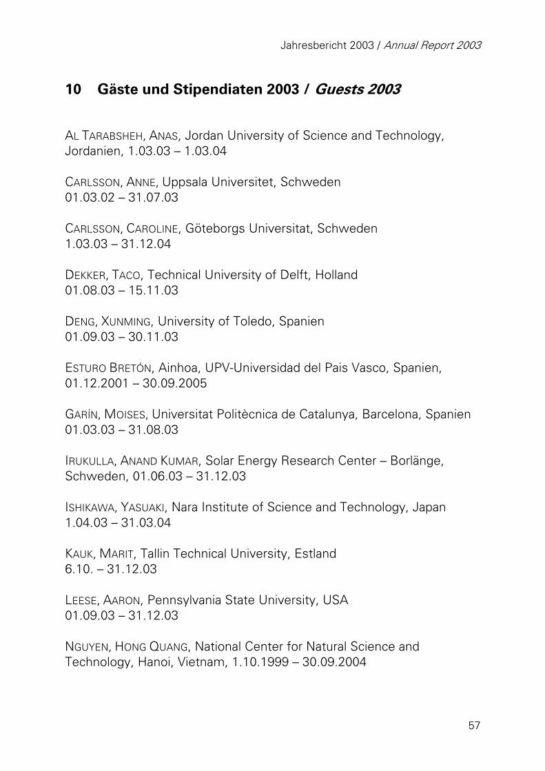
Jahresbericht 2003 / Annual Report 2003
57
10 Gäste und Stipendiaten 2003 / Guests 2003
AL TARABSHEH, ANAS, Jordan University of Science and Technology, Jordanien, 1.03.03 – 1.03.04 CARLSSON, ANNE, Uppsala Universitet, Schweden 01.03.02 – 31.07.03 CARLSSON, CAROLINE, Göteborgs Universitat, Schweden 1.03.03 – 31.12.04 DEKKER, TACO, Technical University of Delft, Holland 01.08.03 – 15.11.03 DENG, XUNMING, University of Toledo, Spanien 01.09.03 – 30.11.03 ESTURO BRETÓN, Ainhoa, UPV-Universidad del Pais Vasco, Spanien, 01.12.2001 – 30.09.2005 GARÍN, MOISES, Universitat Politècnica de Catalunya, Barcelona, Spanien 01.03.03 – 31.08.03 IRUKULLA, ANAND KUMAR, Solar Energy Research Center – Borlänge, Schweden, 01.06.03 – 31.12.03 ISHIKAWA, YASUAKI, Nara Institute of Science and Technology, Japan 1.04.03 – 31.03.04 KAUK, MARIT, Tallin Technical University, Estland 6.10. – 31.12.03 LEESE, AARON, Pennsylvania State University, USA 01.09.03 – 31.12.03 NGUYEN, HONG QUANG, National Center for Natural Science and Technology, Hanoi, Vietnam, 1.10.1999 – 30.09.2004
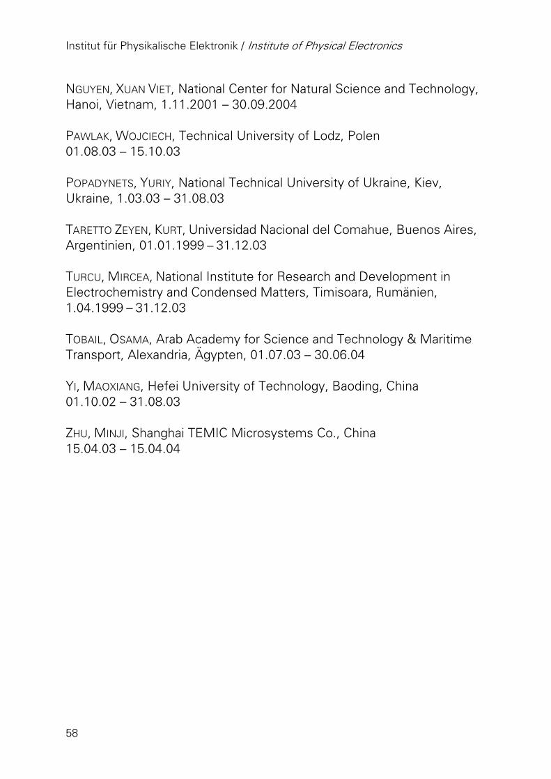
Institut für Physikalische Elektronik / Institute of Physical Electronics
58
NGUYEN, XUAN VIET, National Center for Natural Science and Technology, Hanoi, Vietnam, 1.11.2001 – 30.09.2004 PAWLAK, WOJCIECH, Technical University of Lodz, Polen 01.08.03 – 15.10.03 POPADYNETS, YURIY, National Technical University of Ukraine, Kiev, Ukraine, 1.03.03 – 31.08.03 TARETTO ZEYEN, KURT, Universidad Nacional del Comahue, Buenos Aires, Argentinien, 01.01.1999 – 31.12.03 TURCU, MIRCEA, National Institute for Research and Development in Electrochemistry and Condensed Matters, Timisoara, Rumänien, 1.04.1999 – 31.12.03 TOBAIL, OSAMA, Arab Academy for Science and Technology & Maritime Transport, Alexandria, Ägypten, 01.07.03 – 30.06.04 YI, MAOXIANG, Hefei University of Technology, Baoding, China 01.10.02 – 31.08.03 ZHU, MINJI, Shanghai TEMIC Microsystems Co., China 15.04.03 – 15.04.04
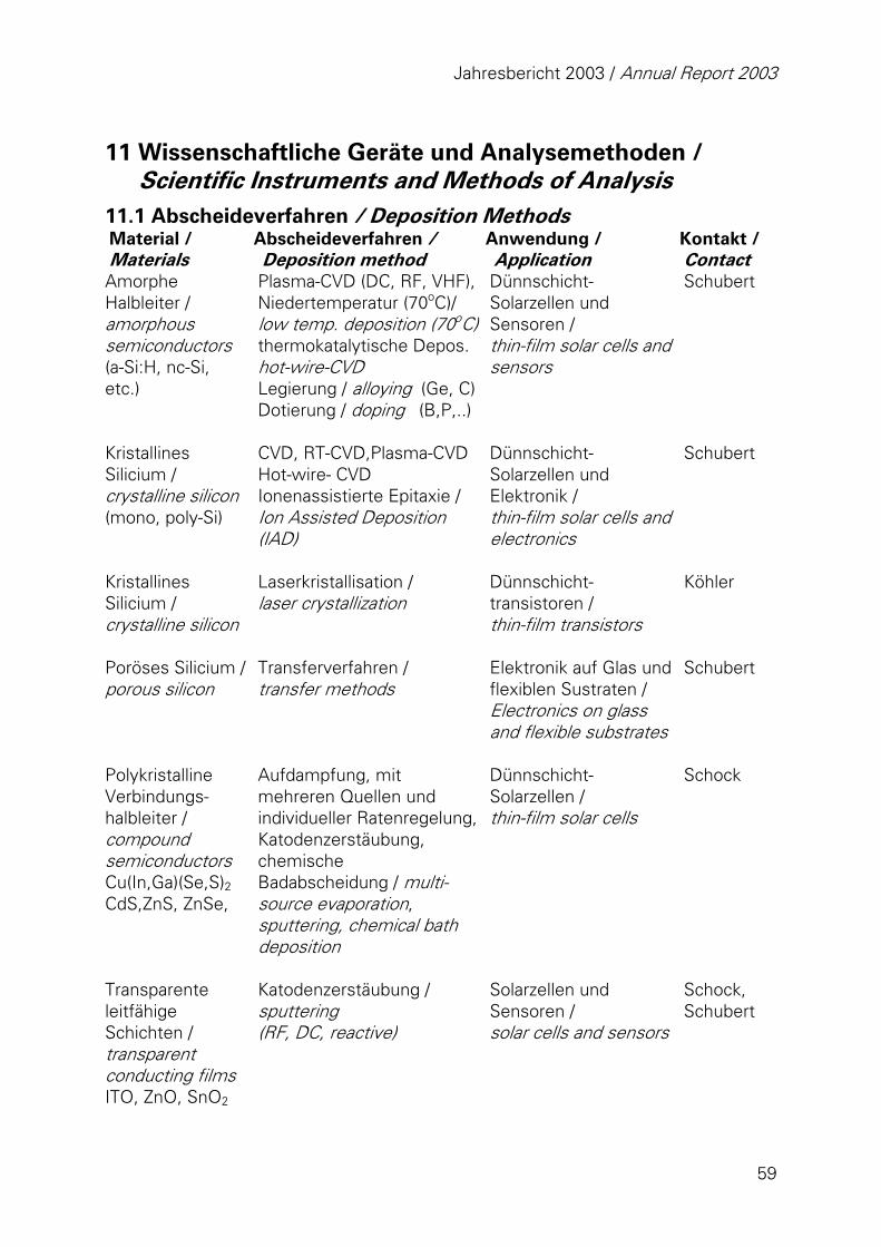
Jahresbericht 2003 / Annual Report 2003
59
11 Wissenschaftliche Geräte und Analysemethoden / Scientific Instruments and Methods of Analysis
11.1 Abscheideverfahren / Deposition Methods Material / Materials
Abscheideverfahren / Deposition method
Anwendung / Application
Kontakt / Contact
Amorphe Halbleiter / amorphous semiconductors (a-Si:H, nc-Si, etc.)
Plasma-CVD (DC, RF, VHF), Niedertemperatur (70oC)/ low temp. deposition (70oC)thermokatalytische Depos. hot-wire-CVD Legierung / alloying (Ge, C) Dotierung / doping (B,P,..)
Dünnschicht-Solarzellen und Sensoren / thin-film solar cells and sensors
Schubert
Kristallines Silicium / crystalline silicon (mono, poly-Si)
CVD, RT-CVD,Plasma-CVD Hot-wire- CVD Ionenassistierte Epitaxie / Ion Assisted Deposition (IAD)
Dünnschicht-Solarzellen und Elektronik / thin-film solar cells and electronics
Schubert
Kristallines Silicium / crystalline silicon
Laserkristallisation / laser crystallization
Dünnschicht-transistoren / thin-film transistors
Köhler
Poröses Silicium / porous silicon
Transferverfahren / transfer methods
Elektronik auf Glas und flexiblen Sustraten / Electronics on glass and flexible substrates
Schubert
Polykristalline Verbindungs-halbleiter / compound semiconductors Cu(In,Ga)(Se,S)2 CdS,ZnS, ZnSe,
Aufdampfung, mit mehreren Quellen und individueller Ratenregelung,Katodenzerstäubung, chemische Badabscheidung / multi-source evaporation, sputtering, chemical bath deposition
Dünnschicht-Solarzellen / thin-film solar cells
Schock
Transparente leitfähige Schichten / transparent conducting films ITO, ZnO, SnO2
Katodenzerstäubung / sputtering (RF, DC, reactive)
Solarzellen und Sensoren / solar cells and sensors
Schock, Schubert
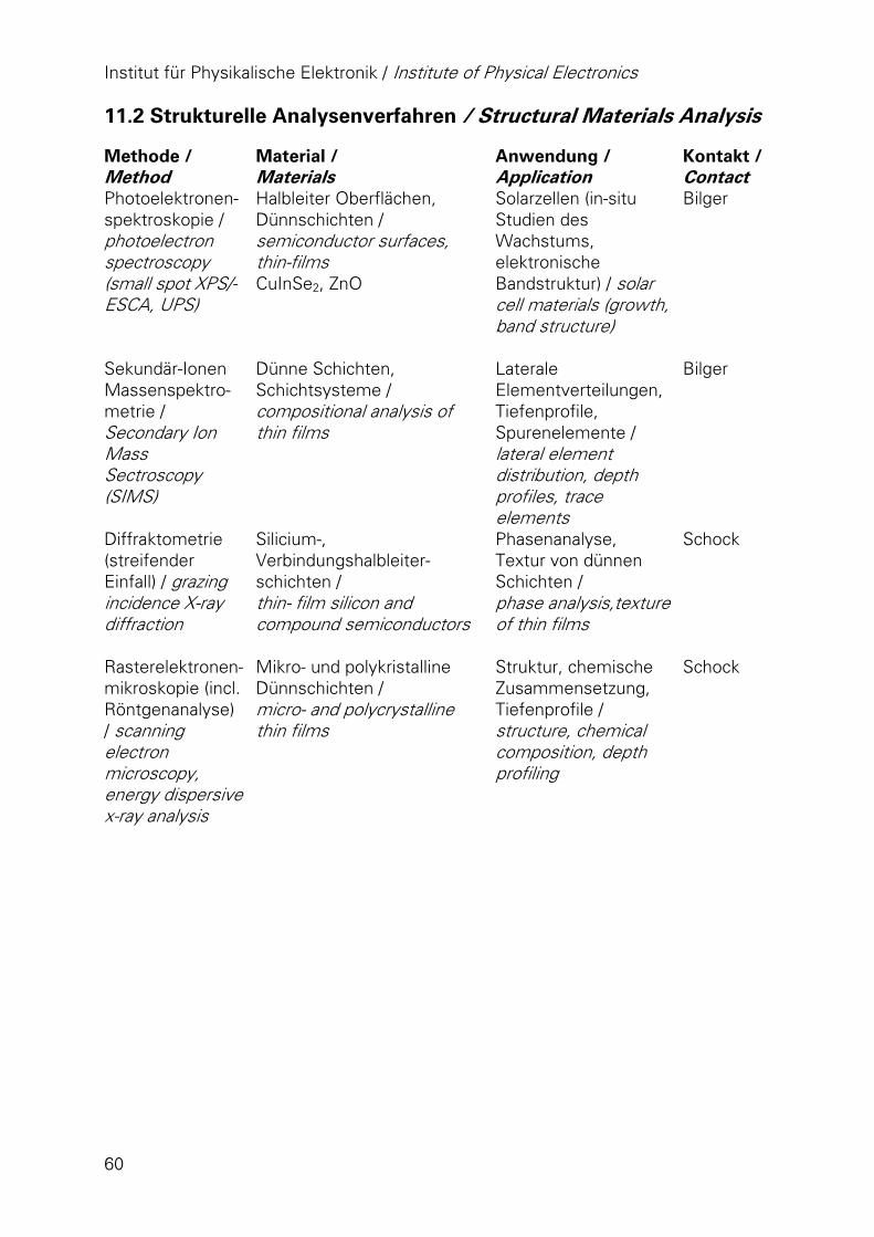
Institut für Physikalische Elektronik / Institute of Physical Electronics
60
11.2 Strukturelle Analysenverfahren / Structural Materials Analysis Methode / Method
Material / Materials
Anwendung / Application
Kontakt / Contact
Photoelektronen-spektroskopie / photoelectron spectroscopy (small spot XPS/-ESCA, UPS)
Halbleiter Oberflächen, Dünnschichten / semiconductor surfaces, thin-films CuInSe2, ZnO
Solarzellen (in-situ Studien des Wachstums, elektronische Bandstruktur) / solar cell materials (growth, band structure)
Bilger
Sekundär-Ionen Massenspektro-metrie / Secondary Ion Mass Sectroscopy (SIMS)
Dünne Schichten, Schichtsysteme / compositional analysis of thin films
Laterale Elementverteilungen, Tiefenprofile, Spurenelemente / lateral element distribution, depth profiles, trace elements
Bilger
Diffraktometrie (streifender Einfall) / grazing incidence X-ray diffraction
Silicium-, Verbindungshalbleiter-schichten / thin- film silicon and compound semiconductors
Phasenanalyse, Textur von dünnen Schichten / phase analysis,texture of thin films
Schock
Rasterelektronen-mikroskopie (incl. Röntgenanalyse) / scanning electron microscopy, energy dispersive x-ray analysis
Mikro- und polykristalline Dünnschichten / micro- and polycrystalline thin films
Struktur, chemische Zusammensetzung, Tiefenprofile / structure, chemical composition, depth profiling
Schock
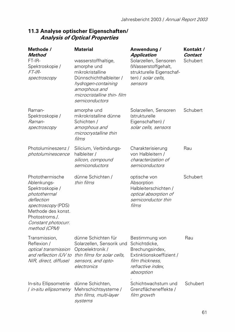
Jahresbericht 2003 / Annual Report 2003
61
11.3 Analyse optischer Eigenschaften/ Analysis of Optical Properties Methode / Method
Material Anwendung / Application
Kontakt / Contact
FT-IR- Spektroskopie / FT-IR- spectroscopy
wasserstoffhaltige, amorphe und mikrokristalline Dünnschichthalbleiter / hydrogen-containing amorphous and microcristalline thin- film semiconductors
Solarzellen, Sensoren (Wasserstoffgehalt, strukturelle Eigenschaf-ten) / solar cells, sensors
Schubert
Raman-Spektroskopie / Raman-spectroscopy
amorphe und mikrokristalline dünne Schichten / amorphous and microcrystalline thin films
Solarzellen, Sensoren (strukturelle Eigenschaften) / solar cells, sensors
Schubert
Photolumineszenz / photoluminescence
Silicium, Verbindungs-halbleiter / silicon, compound semiconductors
Charakterisierung von Halbleitern / characterization of semiconductors
Rau
Photothermische Ablenkungs-Spektroskopie / photothermal deflection spectroscopy (PDS) Methode des konst. Photostroms./. Constant photocurr. method (CPM)
dünne Schichten / thin films
optische von Absorption Halbleiterschichten / optical absorption of semiconductor thin films
Schubert
Transmission, Reflexion / optical transmission and reflection (UV to NIR, direct, diffuse)
dünne Schichten für Solarzellen, Sensorik und Optoelektronik / thin films for solar cells, sensors, and opto-electronics
Bestimmung von Schichtdicke, Brechungsindex, Extinktionskoeffizient / film thickness, refractive index, absorption .
Rau
In-situ Ellipsometrie / in-situ ellipsometry
dünne Schichten, Mehrschichtsysteme / thin films, multi-layer systems
Schichtwachstum und Grenzflächeneffekte / film growth
Schubert
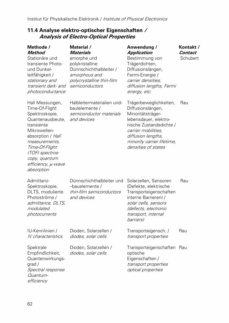
Institut für Physikalische Elektronik / Institute of Physical Electronics
62
11.4 Analyse elektro-optischer Eigenschaften / Analysis of Electro-Optical Properties Methode / Method
Material / Materials
Anwendung / Application
Kontakt / Contact
Stationäre und transiente Photo- und Dunkel-leitfähigkeit / stationary and transient dark- and photoconductance
amorphe und polykristalline Dünnschichthalbleiter / amorphous and polycrystalline thin-film semiconductors
Bestimmung von Trägerdichten, Diffusionslängen, Fermi-Energie / carrier densities, diffusion lengths, Fermi energy, etc.
Schubert
Hall Messungen, Time-Of-Flight Spektroskopie, Quantenausbeute, transiente Mikrowellen-absorption / Hall measurements, Time-Of-Flight (TOF) spectros-copy, quantum efficiency, µ-wave absorption
Halbleitermaterialien und-baulelemente / semiconductor materials and devices
Trägerbeweglichkeiten, Diffusionslängen, Minoritätsträger-lebensdauer, elektro-nische Zustandsdichte / carrier mobilities, diffusion lengths, minority carrier lifetime, densities of states
Rau
Admittanz-Spektroskopie, DLTS, modulierte Photoströme / admittance, DLTS, modulated photocurrents
Dünnschichthalbleiter und –bauelemente / thin-film semiconductors and devices
Solarzellen, Sensoren (Defekte, elektrische Transporteigenschaften interne Barrieren) / solar cells, sensors (defects, electronic transport, internal barriers)
Rau
IU-Kennlinien / IV characteristics
Dioden, Solarzellen / diodes, solar cells
Transporteigensch. / transport properties
Rau
Spektrale Empfindlichkeit, Quantenwirkungs-grad / Spectral response Quantum- efficiency
Dioden, Solarzellen / diodes, solar cells
Transporteigenschaften optische Eigenschaften / transport properties optical properties
Rau
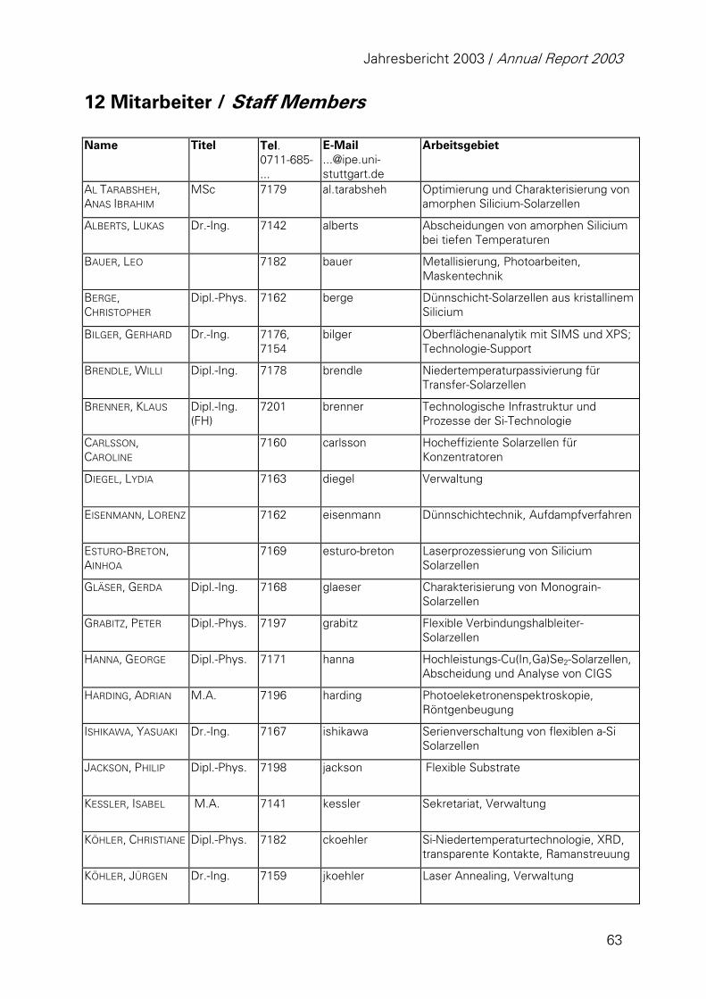
Jahresbericht 2003 / Annual Report 2003
63
12 Mitarbeiter / Staff Members Name Titel Tel.
0711-685-...
E-Mail [email protected]
Arbeitsgebiet
AL TARABSHEH, ANAS IBRAHIM
MSc 7179 al.tarabsheh Optimierung und Charakterisierung von amorphen Silicium-Solarzellen
ALBERTS, LUKAS Dr.-Ing. 7142 alberts Abscheidungen von amorphen Silicium bei tiefen Temperaturen
BAUER, LEO 7182 bauer Metallisierung, Photoarbeiten, Maskentechnik
BERGE, CHRISTOPHER
Dipl.-Phys. 7162 berge Dünnschicht-Solarzellen aus kristallinem Silicium
BILGER, GERHARD Dr.-Ing. 7176, 7154
bilger Oberflächenanalytik mit SIMS und XPS; Technologie-Support
BRENDLE, WILLI Dipl.-Ing. 7178 brendle Niedertemperaturpassivierung für Transfer-Solarzellen
BRENNER, KLAUS Dipl.-Ing. (FH)
7201 brenner Technologische Infrastruktur und Prozesse der Si-Technologie
CARLSSON, CAROLINE
7160 carlsson Hocheffiziente Solarzellen für Konzentratoren
DIEGEL, LYDIA 7163 diegel Verwaltung
EISENMANN, LORENZ 7162 eisenmann Dünnschichtechnik, Aufdampfverfahren
ESTURO-BRETON, AINHOA
7169 esturo-breton Laserprozessierung von Silicium Solarzellen
GLÄSER, GERDA Dipl.-Ing. 7168 glaeser Charakterisierung von Monograin-Solarzellen
GRABITZ, PETER Dipl.-Phys. 7197 grabitz Flexible Verbindungshalbleiter-Solarzellen
HANNA, GEORGE Dipl.-Phys. 7171 hanna Hochleistungs-Cu(In,Ga)Se2-Solarzellen, Abscheidung und Analyse von CIGS
HARDING, ADRIAN M.A. 7196 harding Photoeleketronenspektroskopie, Röntgenbeugung
ISHIKAWA, YASUAKI Dr.-Ing. 7167 ishikawa Serienverschaltung von flexiblen a-Si Solarzellen
JACKSON, PHILIP Dipl.-Phys. 7198 jackson Flexible Substrate
KESSLER, ISABEL M.A. 7141 kessler Sekretariat, Verwaltung
KÖHLER, CHRISTIANE Dipl.-Phys. 7182 ckoehler Si-Niedertemperaturtechnologie, XRD, transparente Kontakte, Ramanstreuung
KÖHLER, JÜRGEN Dr.-Ing. 7159 jkoehler Laser Annealing, Verwaltung
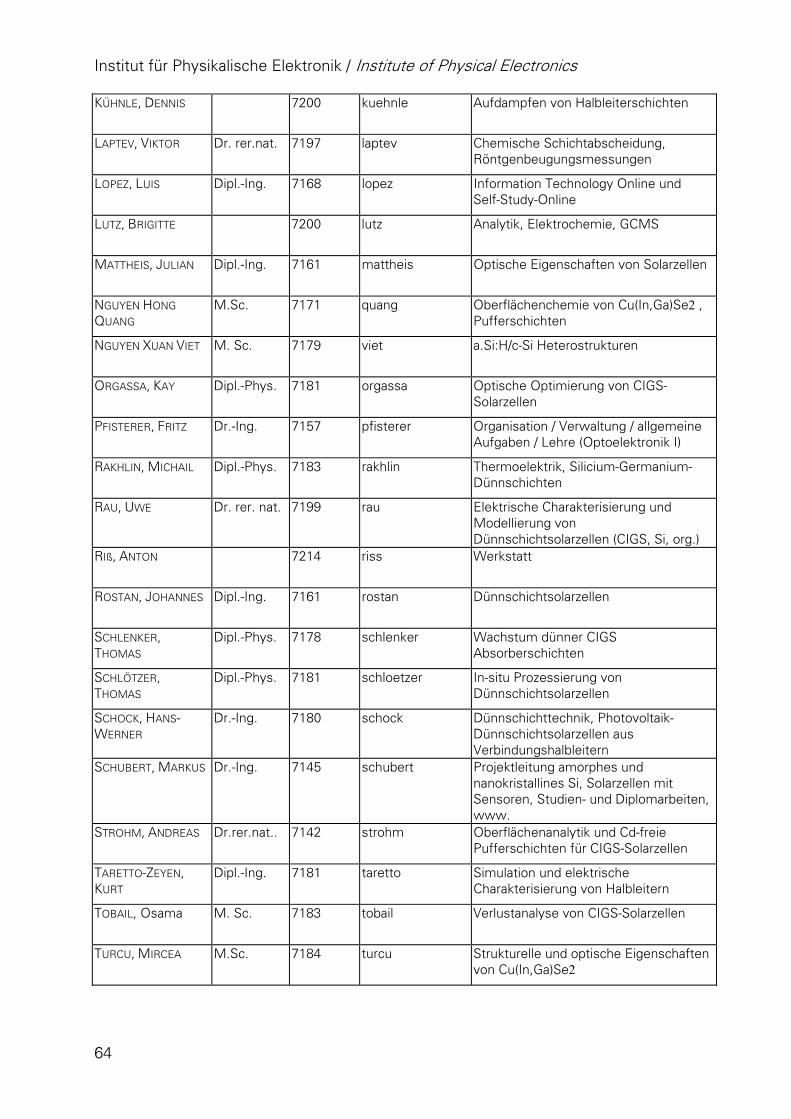
Institut für Physikalische Elektronik / Institute of Physical Electronics
64
KÜHNLE, DENNIS 7200 kuehnle Aufdampfen von Halbleiterschichten
LAPTEV, VIKTOR Dr. rer.nat. 7197 laptev Chemische Schichtabscheidung, Röntgenbeugungsmessungen
LOPEZ, LUIS Dipl.-Ing. 7168 lopez Information Technology Online und Self-Study-Online
LUTZ, BRIGITTE 7200 lutz Analytik, Elektrochemie, GCMS
MATTHEIS, JULIAN Dipl.-Ing. 7161 mattheis Optische Eigenschaften von Solarzellen
NGUYEN HONG
QUANG M.Sc. 7171 quang Oberflächenchemie von Cu(In,Ga)Se2 ,
Pufferschichten
NGUYEN XUAN VIET M. Sc. 7179 viet a.Si:H/c-Si Heterostrukturen
ORGASSA, KAY Dipl.-Phys. 7181 orgassa Optische Optimierung von CIGS-Solarzellen
PFISTERER, FRITZ Dr.-Ing. 7157 pfisterer Organisation / Verwaltung / allgemeine Aufgaben / Lehre (Optoelektronik I)
RAKHLIN, MICHAIL Dipl.-Phys. 7183 rakhlin Thermoelektrik, Silicium-Germanium-Dünnschichten
RAU, UWE Dr. rer. nat. 7199 rau Elektrische Charakterisierung und Modellierung von Dünnschichtsolarzellen (CIGS, Si, org.)
RIß, ANTON 7214 riss Werkstatt
ROSTAN, JOHANNES Dipl.-Ing. 7161 rostan Dünnschichtsolarzellen
SCHLENKER, THOMAS
Dipl.-Phys. 7178 schlenker Wachstum dünner CIGS Absorberschichten
SCHLÖTZER, THOMAS
Dipl.-Phys. 7181 schloetzer In-situ Prozessierung von Dünnschichtsolarzellen
SCHOCK, HANS-WERNER
Dr.-Ing. 7180 schock Dünnschichttechnik, Photovoltaik-Dünnschichtsolarzellen aus Verbindungshalbleitern
SCHUBERT, MARKUS Dr.-Ing. 7145 schubert Projektleitung amorphes und nanokristallines Si, Solarzellen mit Sensoren, Studien- und Diplomarbeiten, www.
STROHM, ANDREAS Dr.rer.nat.. 7142 strohm Oberflächenanalytik und Cd-freie Pufferschichten für CIGS-Solarzellen
TARETTO-ZEYEN, KURT
Dipl.-Ing. 7181 taretto Simulation und elektrische Charakterisierung von Halbleitern
TOBAIL, Osama M. Sc. 7183 tobail Verlustanalyse von CIGS-Solarzellen
TURCU, MIRCEA M.Sc. 7184 turcu Strukturelle und optische Eigenschaften von Cu(In,Ga)Se2
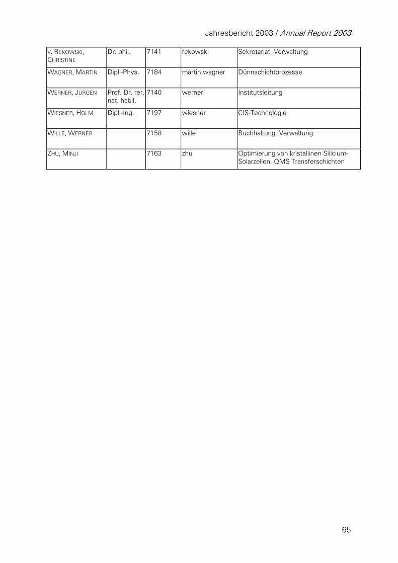
Jahresbericht 2003 / Annual Report 2003
65
V. REKOWSKI, CHRISTINE
Dr. phil. 7141 rekowski Sekretariat, Verwaltung
WAGNER, MARTIN Dipl.-Phys. 7184 martin.wagner Dünnschichtprozesse
WERNER, JÜRGEN Prof. Dr. rer. nat. habil.
7140 werner Institutsleitung
WIESNER, HOLM Dipl.-Ing. 7197 wiesner CIS-Technologie
WILLE, WERNER 7158 wille Buchhaltung, Verwaltung
ZHU, MINJI 7163 zhu Optimierung von kristallinen Silicium-Solarzellen, QMS Transferschichten

Institut für Physikalische Elektronik / Institute of Physical Electronics
66
13 Lageplan / Site Plan
BundesautobahnHighway
MünchenA8A8
AutobahnkreuzStuttgart-Vaihingen
Max-Planck-Institute
AirportFlughafenStuttgart
Karlsruhe, Basel,Frankfurt, Heilbronn,Heidelberg, Würzburg
SingenA831
A831
B14
Schwabstraße
NürnbergWaiblingen
Main StaitonBus Stop to / from Airport
Hauptbahnhof
FeuerseeStadtmitte
Uni-versität
Universität Stuttgart-VaihingenCampus
Vaihingen
Österfeld
ExitUniversität
StuttgartZentrum
Degerloch
ExitDegerlochRohr
Oberaichen Leinfelden Echterdingen
SS
SS
S
S
S
S
S
pe
S S S
B14 Exit
Universität
pe
S
P
PP
PP
P
P
P
PP
P
PP
Pfa
ffenw
aldr
ing
Universit
ätsstraße
Allmandring
S
PPP
P
ß