Embed Size (px)
Citation preview
Assessment of improvement of extension of reach
of 10 Gbps PONs by using APDs
Joao Adriano Ramalho Mourato
Thesis to obtain the Master of Science Degree in
Electrical and Computer Engineering
Supervisor: Prof. Dr. Adolfo da Visitacao Tregeira Cartaxo
Examination Committee
Chairperson: Prof. Dr. Jose Eduardo Charters Ribeiro da Cunha SanguinoSupervisor: Prof. Dr. Adolfo da Visitacao Tregeira CartaxoMembers of the Committee: Prof. Paula Raquel Laurencio
July 2015

ii

Acknowledgements
This dissertation would not have been possible without the support and encouragement of many
people throughout my education, whether explicitly mentioned here or not, and to these people
I express my sincere appreciation.
Firstly, I would like to express my deepest gratitude to my supervisor Associate Professor
Adolfo Cartaxo for the high quality of his academic advice and direction, and for his generous
help, patience and support throughout the development of this dissertation.
I would like to thank my family for all the love and unequivocal support they always gave
me and keep giving. Without your support and understanding I would never have been able to
finish this dissertation. This work is dedicated to you: Margarida Conceicao Ribeiro Ramalho
and Antonio Mao de Ferro Mourato. I also dedicate this work to sibling, Antonio Mourato.
Last, but by no means least, I would like to thank all my friends, without your encour-
agement, patience and example this dissertation would not have materialized. Luıs Mendes,
Joao Rafael, Pedro Freitas, Frederico Alcobia and Joao Augusto for all the good moments and
support you have provided to me along my graduation and master courses. Thank you all.
iii

iv
Abstract
The 10 gigabit per second passive optical network (XG-PON) standard was proposed to be em-
ployed in optical fibre telecommunication systems due to the increase in binary rate, possibility
of more users in the same PON and non-intrusive deployment on the existing optical access net-
work. The PON systems can use the Positive-Intrinsic-Negative diode (PIN) or the Avalanche
Photodiode (APD) as photodetector. However, the high bitrate increases the effect of the mode
partition noise (MPN). Therefore, the study of the photodetector performance in the presence
of the MPN is of special concern.
In this dissertation, the models that characterize the APD and MPN are described and their
impact on the performance of 10 Gbps PON is assessed through numerical computation. In
addition, for optimizing the performance of the APD on the XG-PON system, for non-null ex-
tinction ratio, an expression for the APD sensitivity is proposed.
The XG-PON, comprising the use of multi-longitudinal mode (MLM) lasers or single lon-
gitudinal mode (SLM) lasers at the optical line termination (OLT) and the optical network unit
(ONU), is evaluated. For a dispersion parameter value of 18.41 ps/(nm.km) in the downstream
and a dispersion parameter value of ´3.68 ps/(nm.km) in the upstream, MLM lasers cannot
be used in either direction. Moreover, the effect of the MPN on the signal from SLM lasers
is negligible, provided that the side-mode suppression ratio (SMSR) is high (SMSR ě 30 dB).
Furthermore, the average power level emitted by the ONU imposes a limit in the splitting ratio
and maximum distance.
Keywords: XG-PON, avalanche photo-diode, mode partition noise, multi-longitudinal
mode laser, single-longitudinal mode laser.
v

vi
Resumo
Foi proposta, em sistemas de telecomunicacoes por fibra optica, a rede optica passiva a 10
gigabits por segundo (XG-PON) para aumentar o ritmo binario, permitir mais utilizadores na
mesma PON e por ser facil a introducao nas redes de acesso existentes. Pode ser usado o
positivo-intrınseco-negativo (PIN) ou o fotodıodo de avalanche (APD) como fotodetector. No
entanto, o aumento do ritmo binario aumenta tambem o efeito do ruıdo de particao de modos
(MPN). Consequentemente, o estudo do desempenho do receptor na presenca de MPN e de
especial interesse.
Nesta dissertacao, descrevem-se os modelos que caracterizam APD e MPN e o seu impacto
no desempenho de sistemas de PON a 10 Gbps e avaliado atraves de calculos numericos. Alem
disso, e proposta uma expressao para a sensibilidade que tem em conta a razao de extincao, com
o objectivo de optimizar o impacto do APD no sistema XG-PON.
A XG-PON, contemplando o uso de lasers multimodo (MLM) e monomodo (SLM) como
emissores na terminacao optica de linha (OLT) e na unidade optica de rede (ONU), e avaliada.
Para um valor de parametro de dispersao de 18.41 ps/(nm.km) no sentido descendente e ´3.68
ps/(nm.km) no sentido ascendente, os lasers MLM nao podem ser utilizados. Ainda, o efeito
do MPN no sinal produzido por lasers SLM e desprezavel, desde que a razao de supressao do
modo lateral (SMSR) seja suficientemente alta (SMSR ě 30 dB). A potencia de emissao da
ONU e o factor limitativo na distancia maxima e numero de utilizadores.
Palavras-chave: XG-PON, foto-dıodo de avalanche, ruıdo de particao de modos, laser
multimodo, laser monomodo.
vii

viii

Table of Contents
Acknowledgements iii
Abstract v
Resumo vii
Table of Contents ix
List of Figures xiii
List of Tables xv
List of Acronyms xvii
List of Symbols xxi
1 Introduction 1
1.1 Scope of the work . . . . . . . . . . . . . . . . . . . . . . . . . . . . . . . . . 1
1.1.1 Optical access networks . . . . . . . . . . . . . . . . . . . . . . . . . 1
1.1.2 XG-PON . . . . . . . . . . . . . . . . . . . . . . . . . . . . . . . . . 2
1.2 Motivation . . . . . . . . . . . . . . . . . . . . . . . . . . . . . . . . . . . . . 3
1.3 Objectives and structure of the dissertation . . . . . . . . . . . . . . . . . . . . 4
1.4 Main original contributions . . . . . . . . . . . . . . . . . . . . . . . . . . . . 5
2 Characterization of the XG-PON 7
2.1 Introduction to GPON . . . . . . . . . . . . . . . . . . . . . . . . . . . . . . . 7
2.2 XG-PON . . . . . . . . . . . . . . . . . . . . . . . . . . . . . . . . . . . . . 10
2.3 Solutions for transmitter and receiver . . . . . . . . . . . . . . . . . . . . . . . 14
2.3.1 Receiver . . . . . . . . . . . . . . . . . . . . . . . . . . . . . . . . . 15
ix
TABLE OF CONTENTS
2.3.2 Transmitter . . . . . . . . . . . . . . . . . . . . . . . . . . . . . . . . 16
2.4 Conclusion . . . . . . . . . . . . . . . . . . . . . . . . . . . . . . . . . . . . 17
3 APD impact on the system performance 19
3.1 Motivation for using an APD . . . . . . . . . . . . . . . . . . . . . . . . . . . 19
3.2 Principles of APDs . . . . . . . . . . . . . . . . . . . . . . . . . . . . . . . . 20
3.3 Signal characterization . . . . . . . . . . . . . . . . . . . . . . . . . . . . . . 21
3.4 Receiver characterization . . . . . . . . . . . . . . . . . . . . . . . . . . . . . 22
3.5 Noise characterization . . . . . . . . . . . . . . . . . . . . . . . . . . . . . . 24
3.5.1 Thermal noise . . . . . . . . . . . . . . . . . . . . . . . . . . . . . . . 24
3.5.2 Shot noise . . . . . . . . . . . . . . . . . . . . . . . . . . . . . . . . . 24
3.6 APD receiver sensitivity . . . . . . . . . . . . . . . . . . . . . . . . . . . . . 26
3.7 APD improvement over PIN . . . . . . . . . . . . . . . . . . . . . . . . . . . 28
3.8 Analysis of sensitivity variation . . . . . . . . . . . . . . . . . . . . . . . . . . 32
3.9 Optimum avalanche gain . . . . . . . . . . . . . . . . . . . . . . . . . . . . . 36
3.10 Conclusion . . . . . . . . . . . . . . . . . . . . . . . . . . . . . . . . . . . . 39
4 MPN impact on the system performance 41
4.1 Basic concepts of semiconductor lasers . . . . . . . . . . . . . . . . . . . . . 41
4.2 Characterization of MPN . . . . . . . . . . . . . . . . . . . . . . . . . . . . . 43
4.3 MPN modeling . . . . . . . . . . . . . . . . . . . . . . . . . . . . . . . . . . 44
4.3.1 Mode-partition coefficient . . . . . . . . . . . . . . . . . . . . . . . . 46
4.3.2 Mode-partition noise . . . . . . . . . . . . . . . . . . . . . . . . . . . 47
4.4 MPN in MLM lasers . . . . . . . . . . . . . . . . . . . . . . . . . . . . . . . 48
4.5 MPN in SLM lasers . . . . . . . . . . . . . . . . . . . . . . . . . . . . . . . . 49
4.6 Penalty for using a MLM laser . . . . . . . . . . . . . . . . . . . . . . . . . . 52
4.7 Penalty for using a SLM laser . . . . . . . . . . . . . . . . . . . . . . . . . . 53
4.8 Conclusion . . . . . . . . . . . . . . . . . . . . . . . . . . . . . . . . . . . . 55
5 Assessment of XG-PON reach improvement 57
5.1 Link budget of the XG-PON system . . . . . . . . . . . . . . . . . . . . . . . 57
5.2 Improvement using MLM lasers . . . . . . . . . . . . . . . . . . . . . . . . . 60
5.2.1 Downstream . . . . . . . . . . . . . . . . . . . . . . . . . . . . . . . 60
5.2.2 Upstream . . . . . . . . . . . . . . . . . . . . . . . . . . . . . . . . . 61
x

TABLE OF CONTENTS
5.3 Improvement using SLM lasers . . . . . . . . . . . . . . . . . . . . . . . . . . 62
5.3.1 Downstream . . . . . . . . . . . . . . . . . . . . . . . . . . . . . . . 62
5.3.2 Upstream . . . . . . . . . . . . . . . . . . . . . . . . . . . . . . . . . 64
5.4 Conclusion . . . . . . . . . . . . . . . . . . . . . . . . . . . . . . . . . . . . 66
6 Conclusion and future work 67
6.1 Final conclusions . . . . . . . . . . . . . . . . . . . . . . . . . . . . . . . . . 67
6.2 Future work . . . . . . . . . . . . . . . . . . . . . . . . . . . . . . . . . . . . 69
References 71
A APD receiver sensitivity with finite extinction ratio 75
A.1 Bit error rate . . . . . . . . . . . . . . . . . . . . . . . . . . . . . . . . . . . . 75
A.2 Preparatory steps . . . . . . . . . . . . . . . . . . . . . . . . . . . . . . . . . 77
A.3 Deriving APD sensitivity expression . . . . . . . . . . . . . . . . . . . . . . . 79
A.4 APD sensitivity applied to PIN . . . . . . . . . . . . . . . . . . . . . . . . . . 81
A.5 Deriving the APD optimum gain . . . . . . . . . . . . . . . . . . . . . . . . . 81
B Auxiliary derivations related to MPN 85
B.1 BER in SLM lasers . . . . . . . . . . . . . . . . . . . . . . . . . . . . . . . . 85
B.1.1 BER particular cases . . . . . . . . . . . . . . . . . . . . . . . . . . . 91
B.2 BER in SLM lasers based on Gaussian approximation . . . . . . . . . . . . . . 93
B.2.1 BER derivation . . . . . . . . . . . . . . . . . . . . . . . . . . . . . . 93
B.3 Validation of the model used to obtain BER . . . . . . . . . . . . . . . . . . . 98
xi

TABLE OF CONTENTS
xii
List of Figures
2.1 GPON system example. . . . . . . . . . . . . . . . . . . . . . . . . . . . . . . 8
2.2 GPON and XG-PON coexistence example, assuming every ONU has a WDW
filter. . . . . . . . . . . . . . . . . . . . . . . . . . . . . . . . . . . . . . . . . 13
2.3 XG-PON possible OLT-ONU pairs, according to the XG-PON power budgets. . 16
3.1 Avalanche photo-diode reach-through schematic. . . . . . . . . . . . . . . . . 20
3.2 Optical receiver structure. . . . . . . . . . . . . . . . . . . . . . . . . . . . . . 23
3.3 Variation of the excess noise factor with avalanche gain for several values of kA. 26
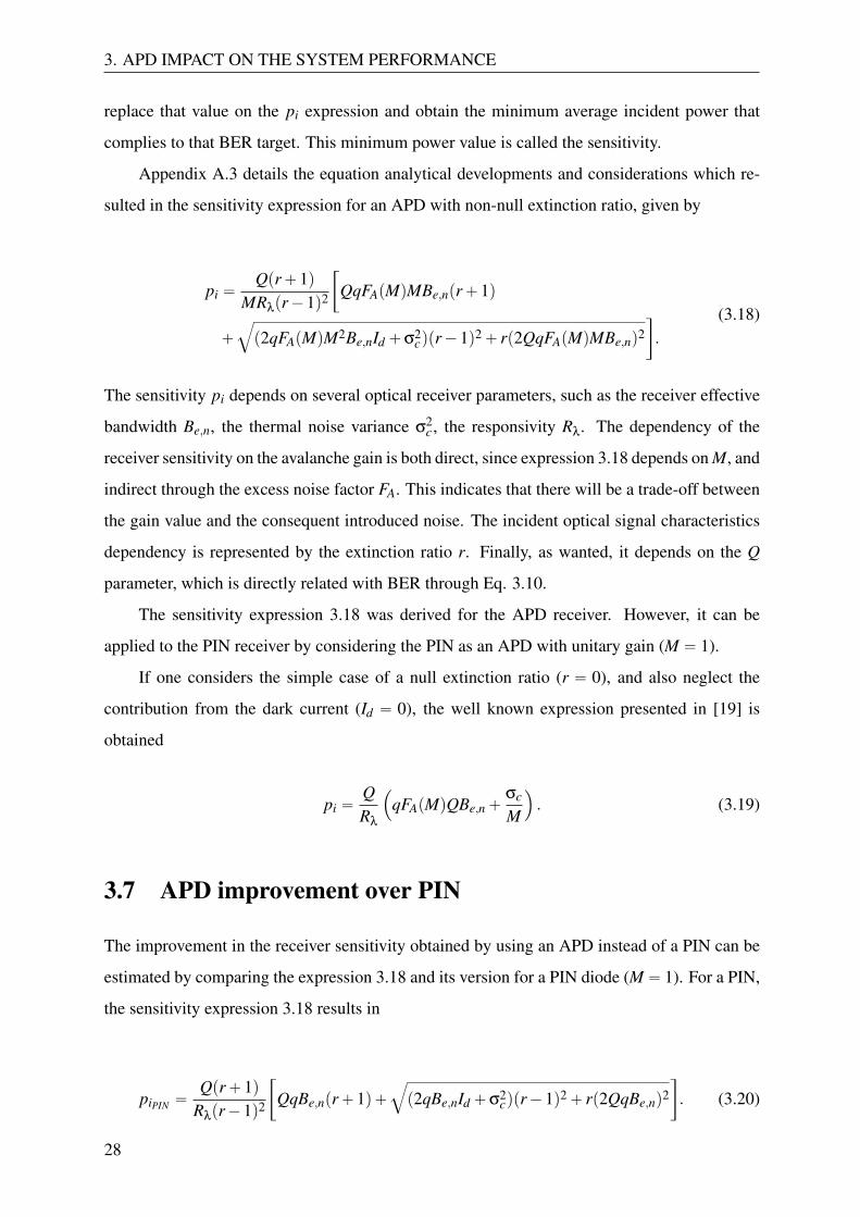
3.4 Sensitivity improvement by using APD instead of a PIN diode. . . . . . . . . . 30
3.5 Sensitivity improvement by using APD instead of a PIN diode for three values
of extinction ratio for kA “ 0.1. . . . . . . . . . . . . . . . . . . . . . . . . . . 30
3.6 Sensitivity improvement by using APD instead of a PIN diode for three values
of extinction ratio for kA “ 0.5. . . . . . . . . . . . . . . . . . . . . . . . . . . 31
3.7 Sensitivity improvement by using APD instead of a PIN diode for three values
of extinction ratio for kA “ 1.0. . . . . . . . . . . . . . . . . . . . . . . . . . . 32
3.8 Sensitivity variation with the avalanche gain for Ge, InGaAs and Si APDs. . . . 33
3.9 Sensitivity variation with the effective noise bandwidth value for kA “ 0.45 and
r “ 0.152. . . . . . . . . . . . . . . . . . . . . . . . . . . . . . . . . . . . . . 34
3.10 Sensitivity variation with the ionization coefficient ratio value for Be,n “ 8 GHz
and r “ 0.152. . . . . . . . . . . . . . . . . . . . . . . . . . . . . . . . . . . . 35
3.11 Sensitivity dependence on the extinction ratio value Be,n “ 8 GHz and kA “ 0.45. 36
3.12 Sensitivity versus sensitivity approximation, with extinction ratio r “ 0.05. . . 37
3.13 Sensitivity versus sensitivity approximation, with extinction ratio r “ 0.1. . . . 38
3.14 Sensitivity versus sensitivity approximation, with extinction ratio r “ 0.152. . . 38
4.1 Random power spectrum at different times t1, t2, for illustrating the partition
noise. . . . . . . . . . . . . . . . . . . . . . . . . . . . . . . . . . . . . . . . 44
xiii
LIST OF FIGURES
4.2 Power penalty when using a MLM laser in function of β parameter, for various
values of kMPN for Q“ 7. . . . . . . . . . . . . . . . . . . . . . . . . . . . . . 52
4.3 Power penalty when using a MLM laser in function of β parameter, for various
values of kMPN for Q“ 3. . . . . . . . . . . . . . . . . . . . . . . . . . . . . . 53
4.4 Relation between the increased power at the receiver and the side-mode sup-
pression ratio, considering a reference BER of 10´12 and r “ 0.1, for M “ 1
and M “ 10. . . . . . . . . . . . . . . . . . . . . . . . . . . . . . . . . . . . . 54
4.5 Relation between the increased power at the receiver and the side-mode sup-
pression ratio, considering a reference BER of 10´12 and M “ 10, for r “ 0.01,
r “ 0.1 and r “ 0.152. . . . . . . . . . . . . . . . . . . . . . . . . . . . . . . 55
A.1 Sensitivity values for both solutions presented. . . . . . . . . . . . . . . . . . . 81
A.2 Sensitivity expression compared against its three components for an extinction
ratio of 0.152 . . . . . . . . . . . . . . . . . . . . . . . . . . . . . . . . . . . . 83
A.3 Sensitivity expression compared against its three components for an extinction
ratio of 0.1 . . . . . . . . . . . . . . . . . . . . . . . . . . . . . . . . . . . . . 83
A.4 Sensitivity expression compared against its three components for an extinction
ratio of 0.05 . . . . . . . . . . . . . . . . . . . . . . . . . . . . . . . . . . . . 84
B.1 Regions of integration of PpI ą ID0q. . . . . . . . . . . . . . . . . . . . . . . . 87
B.2 Region of integration of PpI ă ID1q. . . . . . . . . . . . . . . . . . . . . . . . 88
B.3 Gaussian distribution and noncentral Chi-squared distribution for ψ“ 2ˆ10´4 . 99
B.4 Gaussian distribution and noncentral Chi-squared distribution for ψ“ 5.0625ˆ
10´4. . . . . . . . . . . . . . . . . . . . . . . . . . . . . . . . . . . . . . . . 99
xiv
List of Tables
2.1 Summary of GPON and XG-PON common characteristics. . . . . . . . . . . . 14
2.2 Summary of XG-GPON power budgets. . . . . . . . . . . . . . . . . . . . . . 15
3.1 Set of typical values for sensitivity parameters . . . . . . . . . . . . . . . . . . 29
3.2 Set of typical values for APD receivers . . . . . . . . . . . . . . . . . . . . . . 32
4.1 Parameters used for obtaining numeric results. . . . . . . . . . . . . . . . . . . 54
5.1 Typical parameters of XG-PON system used for obtaining numerical results. . . 59
5.2 Typical G.652 fibre parameters used for obtaining numerical results [34]. . . . 59
5.3 PON split ratios and corresponding losses [35]. . . . . . . . . . . . . . . . . . 59
5.4 Receiver parameters used for obtaining numerical results. . . . . . . . . . . . . 59
5.5 Sensitivities used for obtaining numerical results. . . . . . . . . . . . . . . . . 60
5.6 Emmiting powers for the optical sources of OLT and ONU using MLM and
SLM lasers. . . . . . . . . . . . . . . . . . . . . . . . . . . . . . . . . . . . . 60
5.7 Maximum distance imposed by the power budget and system margin for L“ 20
km, for both PIN and APD receivers as function of the splitter ratio without
FEC, in the downstream direction. . . . . . . . . . . . . . . . . . . . . . . . . 63
5.8 Maximum distance imposed by the power budget and system margin for L“ 20
km, for both PIN and APD receivers as function of the splitter ratio using FEC,
in the downstream direction. . . . . . . . . . . . . . . . . . . . . . . . . . . . 63
5.9 Maximum distance imposed by the power budget and system margin for L“ 20
km, for both PIN and APD receivers as function of the splitter ratio without
FEC, in the upstream direction. . . . . . . . . . . . . . . . . . . . . . . . . . . 64
5.10 Maximum distance imposed by the power budget and system margin for L“ 20
km, for both PIN and APD receivers as function of the splitter ratio using FEC,
in the upstream direction. . . . . . . . . . . . . . . . . . . . . . . . . . . . . . 65
xv

LIST OF TABLES
5.11 Summary of usable splitting ratios for L“ 20 km. . . . . . . . . . . . . . . . . 65
A.1 Set of typical values for sensitivity parameters for testing the two sensitivity
solutions. . . . . . . . . . . . . . . . . . . . . . . . . . . . . . . . . . . . . . 80
xvi

List of Acronyms
Acronym Description
AES Advanced Encryption Standard
AGC Automatic gain control
APD Avalanche photo-diode
APON ATM Passive Optical Network
ATM Asynchronous Transfer Mode
BER Bit Error Ratio
BPON Broadband Passive Optical Network
CAS Client Adaptation Layer
CO Central Office
DBA Dynamic Bandwidth Allocation
DBRu Dynamic Bandwidth Report Upstream
DML Directly Modulated Laser
EFM Ethernet in the First Mile
EML Externally Modulated Laser
EPON Ethernet Passive Optical Network
FP Fabry-Perot
FEC Forward Error Correction
FS Framing Sublayer
xvii

LIST OF ACRONYMS
FSAN Full Service Access Network
FTTH Fibre To The Home
GEM GPON Encapsulation Method
GPON Gigabit Passive Optical Network
GTC GPON Transmission Convergence
HEC Header Correction Code
HSI High Speed Internet
ID Identification
IEEE Institute of Electrical and Electronics Engineers
IP Internet Protocol
ITU International Telecommunications Union
LED Light Emitting Diode
MAC Medium Control Access
MIB ONU Management Base
MLM Multi-longitudinal Mode
MSR Mode-Suppression Ratio
MPN Mode Partition Noise
NRZ Non-Return-to-Zero
ODN Optical Distribution Network
OLT Optical Line Terminal
OMCC ONU Management Control Channel Protocol
OMCI ONU Management Control Interface
ONU Optical Network Unit
PAS PHY Adaptation Sublayer
xviii

LIST OF ACRONYMS
PCBd Physical Control Block Downstream
PHY Physical
PIN Positive-Intrinsic-Negative
PLOAM Physical Layer Operations Administration Maintenance
PLOu Physical Layer Overhead Upstream
PMD Physical Medium Dependent
PON Passive Optical Network
POTS Plain Old Telephone Service
PSBd Physical Synchronization Block Downstream
PSBu Physical Synchronization Block Upstream
QoS Quality Of Service
RMS Root-Mean-Square
SLM Single Longitudinal Mode
SMF Single Mode Fibre
SMSR Side-mode Suppression Ratio
SNR Signal-To-Noise Ratio
TC Transmission Convergence
T-Cont Transmission Container
TDM Time Division Multiplexing
TDMA Time Division Multiple Access
VoIP Voice Over IP
WDM Wavelength-Division Multiplexing
xix

LIST OF ACRONYMS
xx

List of Symbols
Symbol Designation
αMPN power penalty induced by mode partition noise
η quantum efficiency
λ optical wavelength
λ0 optical wavelength of central partition mode
λi optical wavelength of ith partition mode
µ Gaussian distribution mean
ν central frequency of the optical spectrum
σ spectral width
σ0 root square variance of bit 0
σ1 root square variance of bit 1
σ2c thermal noise variance
σGaussian variance of Gaussian distribution
σ2mm variance of the main mode
σ2MPN mode partition noise variance
σn total noise root square variance at receiver
σ2s shot noise variance
σ2s,0 shot noise variance for bit 0
σ2s,1 shot noise variance for bit 1
σ2sm variance of the side mode
σ2T variance of the total current after the receiver
∆λ spacing between partition modes
∆τi relative delay of the ith partition mode
ψ non-central Chi-squared parameter
xxi

LIST OF SYMBOLS
b drop-out rate
B bit rate
Be,n effective noise bandwidth
c speed of light in vacuum
ci normalized amplitude of ith partition mode
dB decibel
Dλ fibre dispersion parameter
erf(¨) error function
erfc(¨) complementary error function
FApMq excess noise factor
Fn circuit noise figure
g semiconductor laser gain coefficient
GAPD gain of apd versus a pin
h Planck’s constant
I0 average bit 0 current
I1 average bit 1 current
Id dark current
ID receiver’s decision threshold current
Imc total multiplied current
Imm current of the main mode
Ip primary unmultiplied current
Ism current of the side mode
IT totl current after the receiver
xxii

LIST OF SYMBOLS
kA ionization coefficient ratio
kB Boltzmann’s constant
kMPN mode partition noise coefficient
L fibre length
Llayer semiconductor laser active-layer length
M avalanche gain
MOptimum optimal avalanche gain
nptq total noise voltage
nGptq Gaussian noise voltage
nexpptq exponential noise voltage
N total number of mode partition modes
pi minimum total incident power
pimode total incident power of ith partition mode
pi,0 incident power for bit 0
pi,1 incident power for bit 1
piPIN minimum total incident power for a PIN diode
PD receiver’s decision threshold power
Pmm single longitudinal mode laser main mode power
Psm single longitudinal mode laser most dominant side mode power
Psmpλiq measured time-average power spectrum of ith partition mode
ptotal total power of signal
q electron charge
Q Q parameter
r extinction ratio
rptq total pulse random response
r0 total pulse random response measured at sample time t0
xxiii

LIST OF SYMBOLS
Rλ unity gain responsivity
RλAPD avalanche gain responsivity
Rext extinction ratio in dB
RL load resistor
T temperature
yiptq partial pulse random response of ith partition mode
xxiv
Chapter 1
Introduction
In this chapter, it is presented an introduction to optical networks, with focus on the last part of
the network, between the user and the service provider, the access network. In section 1.1, the
scope of the work is presented, along with the brief history of the passive optical networks. In
section 1.2, it is presented the motivation for the development of this dissertation. Section 1.3
shows the objectives and structure of this dissertation. Lastly, in section 1.4, the main original
contributions of this dissertation are described.
1.1 Scope of the work
XG-PON has been proposed as an improvement to the deployed PON system, it allowed for
greater bandwidth, users and reach. The scope of this work is to assess the reach improvement
of XG-PON by using single-mode lasers (SLM) or multi-mode lasers (MLM), avalanche pho-
todiodes (APD), and the impact of the Mode Partition Noise (MPN) on the whole system and
its components.
This section presents the principles that support this work: the evolution of the optical ac-
cess networks and the history of Gigabit passive optical network (GPON) technology. The 10
Gigabit PON (XG-PON) is also introduced, in which the work will be focused.
1.1.1 Optical access networks
The evolution of telecommunications technologies and its rapid spread led to a remarkable
growth in the number of applications and services available to the users, resulting in dramatic
increase of demanded bandwidth. Thus, it was necessary to come up with a different approach
1
1. INTRODUCTION
in all segments of the network, in order to satisfy such demand. Focusing on the first mile (also
known as the access network), and in the new generation network technologies, the natural
course of action is to migrate (when possible) from copper solutions towards fibre solutions,
enabling the network to meet the demand. With that purpose in mind, the concept of Pas-
sive Optical Networks (PON) emerged in the mid 90s when the Full Service Access Network
(FSAN) group started working on fibre to the home (FTTH) architectures.
The International Telecommunications Union (ITU) later standardized the PON in its
G.983 recommendation, being the first draft based on Asynchronous Transfer Mode (ATM),
known as ATM PON (APON). However, due to various improvements and the decrease of the
use of ATM as a protocol, the final version of the recommendation came to be commonly re-
ferred as broadband PON (BPON), avoiding the close association with the ATM protocol. Later
in 2001, the FSAN started the development of an enhanced standard that could support multiple
services in their native form, improve the total bandwidth and its efficiency, upgrade the security
and management mechanisms in an evolutionary form. The result was the G.984 recommenda-
tion, also known as GPON.
Around the same time, the Institute of Electrical and Electronics Engineers (IEEE) formed
a task force named Ethernet in the first mile (EFM), which purpose was, as the name states;
bring Ethernet protocol into the access network. The group focused in several areas the most
relevant to our context being the Ethernet over point-to-multipoint fibre (EPON) that was rati-
fied as the IEEE 802.3ah in 2004.
Though progress were made with these technologies, the bandwidth demands of new ap-
plications adding to the increase of users, were, once again, pushing the need for more develop-
ments in the previous presented technologies, in order for them to provide bigger downstream
and upstream rates (per user) as well as extending the reach of the PON, etc. Therefore, recently,
extensions to the above-presented standards were added, resulting in the 10G-EPON ratified in
2009 as 802.3av and the XG-PON (or 10G-PON) as the ITU-T G.987 recommendation, on
which this work will be focusing.
1.1.2 XG-PON
The XG-PON inherits all requirements from the GPON, with a few additions. Also, it must
coexist with the GPON and the overlay video on the same network. One major new feature is the
inclusion of more security. In the original GPON, the threat model assumed that the upstream
2
1.2 Motivation
channel was physically secure, and this motivated a relatively weak security arrangement, which
was strengthened in later amendments to GPON. In XG-PON, the PON system is required to
support the option of strong mutual authentication, and to use the authentication to protect the
integrity of the PON management messages and the PON encryption keys. These enhancements
make it quite difficult for an attacker to masquerade as either an optical network unit (ONU)
or an optical line terminal (OLT), even if he has access to the PON fibres, and even if he can
precisely interleave his transmissions with the victim ONU [10].
To coexist with previous GPON standard, the downstream wavelength of operation of the
XG-PON is in 1575 - 1580 nm window whereas the upstream wavelength of operation of the
XG-PON is in the 1260 - 1280 nm window [2].
The XG-PON was defined as XG-PON1 when a asymmetrical bitrate of 10 Gbps in the
downstream and 2.5 Gbps in the upstream is used. In the case of a symmetrical bitrate, XG-
PON has a bitrate of downstream and upstream of 10 Gbps and it is called XG-PON2.
However when increasing the system rate to a 10 Gbps PON, some limitations arise, mainly
because the cost of the system has to be shared, leading to the use of low-cost equipment at the
user side. This self-imposed restriction has some effects in the performance of such equipment
which results in additional degradation of the system’s performance. This degradation comes
in many forms. However, in the case where the system’s transmission rate is increased, which
is the case that will be focused on, an effect that has very much influence on the system is the
Mode-Partition Noise (MPN) that will be explained later on. Also, the sensitivity of the receiver
itself has performance issues when there is such an increase in the data rate, and then motivating
the need for an evaluation of the receiver, which can be from a common PIN diode receiver to
an Avalanche photo-diode (APD) receiver.
The majority of service providers that employed GPON will skip XG-PON and jump to the next
standard. However, where the GPON is not deployed (i.e. greenfield) the use of the XG-PON
is strong option.
1.2 Motivation
The development of the 10 Gbps PON brings significant advantages to the access network.
The possibility of a higher bitrate per customer or more customers per PON are the obvious
enhancements. The increase of customers per PON leads to the need of a higher splitting ratio.
3
1. INTRODUCTION
The increase in the splitting ratio leads to a lower power level per customer for the same power
at the transmitter output. Thus, the study of the optical receiver employed gains significant
importance.
The higher bitrate may increase dispersion effects such as the MPN. The increase of the
MPN effect leads to an increase of the bit error rate and possibly cripple the link. The MPN
has a different impact on the system depending on the optical source. The nature of the MLM
laser makes it propitious to this type of noise. On the other hand, the SLM laser is in theory less
likely to be affected by this type of noise.
In this dissertation, the implementation of an APD receiver with MLM lasers or SLM
lasers as a solution for the reach increase of the XG-PON system is investigated. Moreover,
with the objective of enhancing the APD performance, an expression for the APD sensitivity
for a non-null extinction ratio is obtained. The degradation of the system performance induced
by the MPN is analysed.
1.3 Objectives and structure of the dissertation
The main objective of this work is to assess the extension of reach in a XG-PON system by
employing an APD receiver instead of a PIN receiver, in the presence of MPN.
This dissertation is composed by 6 chapters and 2 appendixes. The 6 chapters describe
and analyse the results achieved during the dissertation and the 2 appendixes are used to give
support to developed work.
In Chapter 1, the optical networks are presented, particularly, special attention is given to
the access networks. A brief history of the GPON is given, along with the legacy standards.
The XG-PON possible limitations are presented and the motivation for the realization of this
work is described.
In Chapter 2, the GPON standard fundamentals are presented, along with the description
of the basic architecture of a GPON system. The XG-PON system is introduced, and possible
solutions for receiver and transmitter are described.
In Chapter 3, the APD receiver is introduced. The signal at the input of the APD receiver
is characterized, a model for the APD is presented along with the characterization of the noise
after the APD receiver. An expression for the APD receiver sensitivity is proposed and its bene-
fits are evaluated. Also, it is proposed an expression for obtaining the optimum avalanche gain.
4
1.4 Main original contributions
In Chapter 4, the MPN is introduced and studied. The MPN in MLM lasers is studied, and
a model for the MPN in SLM lasers is proposed and evaluated. The effect of the MPN on the bit
error ratio is analysed through the study of the power penalty due to MPN, when using MLM
or SLM lasers.
In Chapter 5, the use of APD receivers in the XG-PON system is evaluated. The assess-
ment tests the possibility of the use of MLM lasers and SLM lasers. The reach extension of the
XG-PON system by using APD receivers instead of PIN is presented.
In Chapter 6, the final conclusions of this dissertation are outlined and proposals for future
work on this subject are made.
In Appendix A, the bit error rate model is described. The APD receiver expression for the
sensitivity is derived, along with the derivation of the APD optimum gain.
In Appendix B, the bit error rate in SLM lasers is described and analysed. A model for
obtaining the BER, based on an approximation, is proposed, and its validation is presented.
1.4 Main original contributions
In the analysis performed in this work, several original contributions were introduced relative
to other studies in the field. In the following, the list of the most important contributions of this
work are presented:
• Derivation of an expression for obtaining the APD sensitivity for non-null extinction ratio,
• Derivation of an expression for the APD optimum gain for non-null extinction ratio,
• Power penalty due to MPN when using MLM lasers based on APD sensitivity expression
for non-null extinction ratio,
• Model for obtaining BER in SLM lasers in the presence of MPN, considering a non-null
extinction ratio,
• Assessment of the XG-PON reach in the presence of MPN by using APDs.
5

1. INTRODUCTION
6
Chapter 2
Characterization of the XG-PON
In this chapter, it is presented the structure of the GPON system followed by the XG-PON sys-
tem. The definition of the two standards is presented, as the XG-PON is very much based on the
GPON. The features of the XG-PON are presented, along with the requirements to implement
it. It is given an overview of the receivers and transmitters that can be employed in the XG-PON
system.
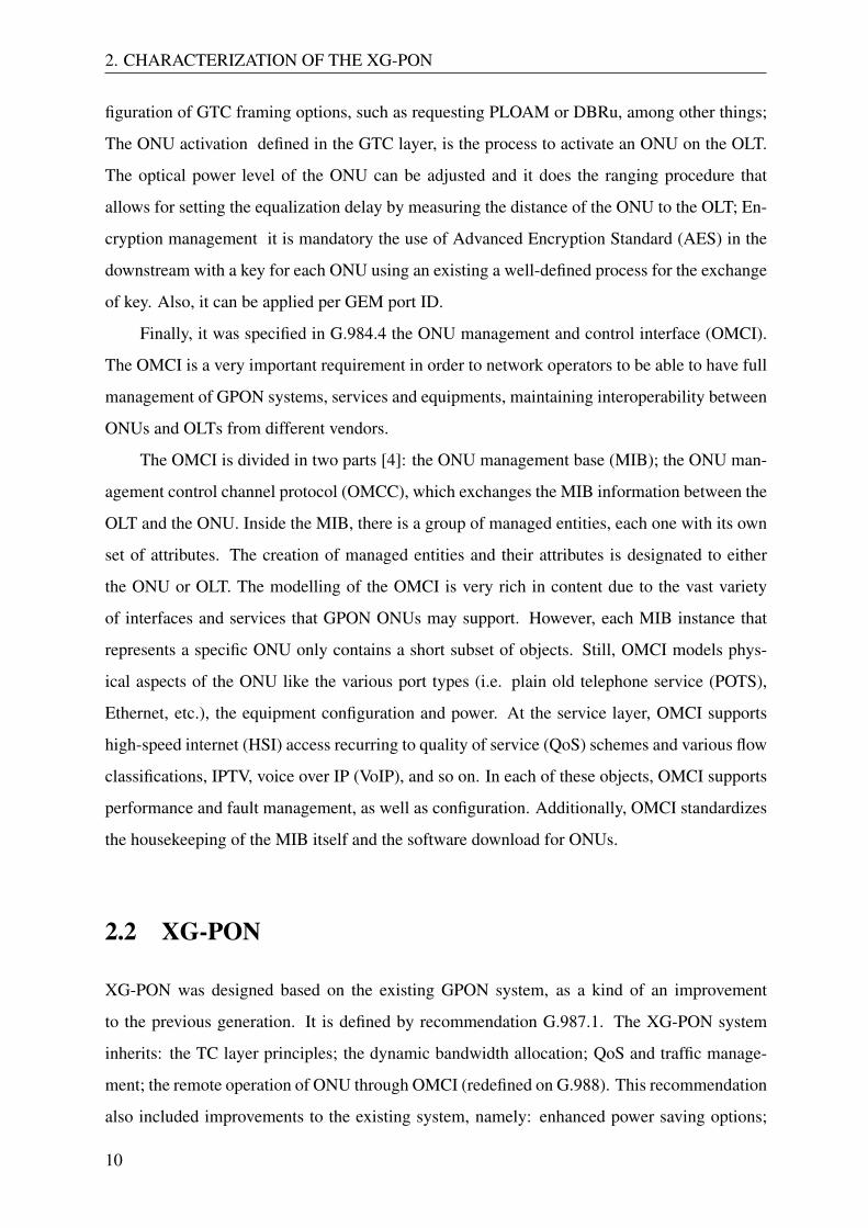
2.1 Introduction to GPON
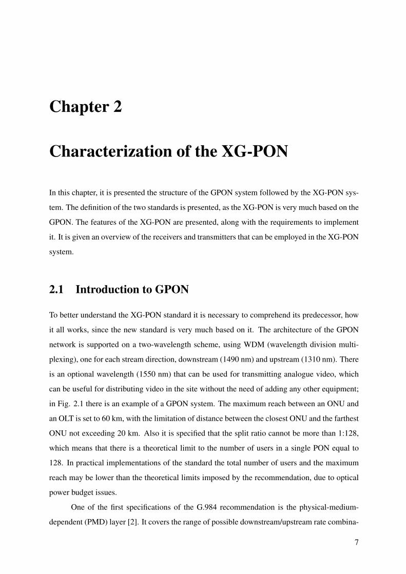
To better understand the XG-PON standard it is necessary to comprehend its predecessor, how
it all works, since the new standard is very much based on it. The architecture of the GPON
network is supported on a two-wavelength scheme, using WDM (wavelength division multi-
plexing), one for each stream direction, downstream (1490 nm) and upstream (1310 nm). There
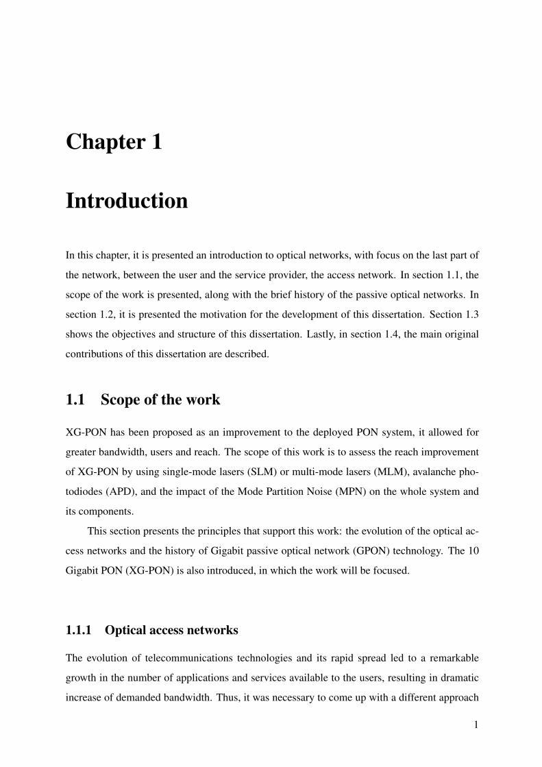
is an optional wavelength (1550 nm) that can be used for transmitting analogue video, which
can be useful for distributing video in the site without the need of adding any other equipment;
in Fig. 2.1 there is an example of a GPON system. The maximum reach between an ONU and
an OLT is set to 60 km, with the limitation of distance between the closest ONU and the farthest
ONU not exceeding 20 km. Also it is specified that the split ratio cannot be more than 1:128,
which means that there is a theoretical limit to the number of users in a single PON equal to
128. In practical implementations of the standard the total number of users and the maximum
reach may be lower than the theoretical limits imposed by the recommendation, due to optical
power budget issues.
One of the first specifications of the G.984 recommendation is the physical-medium-
dependent (PMD) layer [2]. It covers the range of possible downstream/upstream rate combina-
7
2. CHARACTERIZATION OF THE XG-PON
OLT
ONT
ONT
ONT
1:N
WDM
RF Video
Downstream video: 1550 nm
Downstream: 1490 nm Upstream: 1310 nm
Central
Office
Figure 2.1: GPON system example.
tions along with the needed optical parameters for each of them. The preferred combination has
been the 2.488/1.244 Gbps, downstream and upstream respectively, which allowed for optimal
practice for the optical parameters, documented as an amendment to G.984.2. These parameters
are known as class B+ (allows for loss up to 28 dB) and applicable to a network whether it uses
the overlay video (optional third wavelength referred above) or not. The class B+ parameters
are not dependent on the receiver type, PIN or APD.
Part three of the recommendation G.984 is all about the Transmission Convergence layer
(GTC) [3], its main objective is to adapt the user data to the PMD layer. Though, it also provides
some basic management of the GPON network. There are two encapsulation methods allowed
by this specification, the GPON-encapsulation-method (GEM) and the asynchronous transfer
mode (ATM). However, virtually, only the former is used. The use of GEM permits: low over-
head adaptation to several protocols including Ethernet and time-division-multiplexing (TDM);
medium access control (MAC) function; the coordination of the interleaving of upstream trans-
missions from multiple ONUs. In the control plane, there is also the possibility of monitoring
the ONUs health and performance as well as the protocols and procedures for registering an
ONU in the GPON network. GEM offers the possibility to configure features on the transport
level such as the encryption, the bandwidth allocation and the forward error correction (FEC).
Looking into the GTC, there are two sub layers: the lower framing sub layer which defines the
GTC frame structure; the higher sub layer that deals with the TC adaptation through GEM.
In the lower layer, the overhead information is asymmetrical, meaning that the amount of
information is different when in upstream or downstream, however the framing structure does
8
2.1 Introduction to GPON
not vary with different GPON rates, only the size of the payload does.
The downstream GTC has a header containing: all overhead fields; the payload; a phys-
ical control block (PCBd) which includes the bandwidth map field, specifying the ONUs up-
stream transmission allocation; the physical layer operations, administration and maintenance
(PLOAM) field. The PLOAM field has the purpose of carrying a message-based protocol de-
signed for GTC and PMD layer management. It is important to mention that this downstream
frame is a 125us frame and transports an 8 kHz signal to provide a reference clock to the ONUs.
The upstream frame contains a sequence of ONU transmissions, previously dictated by the OLT.
Each of the transmissions frames has physical layer overhead field (PLOu) that includes a
preamble and a delimiter, both configurable by the OLT. The PLOu might have a dynamic band-
width report field, to help the dynamic bandwidth allocation mechanism, which carries traffic
queuing reports from the ONUs. It might also include a similar field to the downstream frame,
a PLOAM field. Both of the two referred fields are optional and only present upon request from
the OLT.
On the other hand, the higher layer is based on GEM, which defines a connection-oriented
encapsulation, independently of the protocol, with variable size packets. GEM has a virtual
connection unit with the name GEM port, where it contains the flows between logical and phys-
ical ports of an ONU. The port ID and the size of the frame are included in a 5-byte header
of the GEM frame. This frame can be fragmented which means a single packet can be split in
many GEM frames. The recommendation G.984.3 has appendices for the specification on the
transport of native TDM and Ethernet over GEM.
There is a unit for the upstream bandwidth allocation by the OLT named transmission
container (T-cont), configurable by the OLT. The most common configuration is based on one
T-cont per service class per ONU, or just a single T-cont per ONU. GEM ports are bundled onto
T-cont’s.
Bandwidth allocation can be done either in static method or dynamic (DBA). In GPON
there are two DBA defined methods: status-reporting DBA and non-status-reporting. The for-
mer is based on reports from the ONU via DBRu field in the upstream frame. The later consists
in monitoring T-cont utilization by the OLT. The control plane of the GTC layer is mainly
based on the PLOAM message protocol and some other overhead fields. The management op-
tions available include: PMD layer management - monitoring health of the physical layer and
generation of statistics and alarms when pertinent; GTC layer management related to the con-
9
2. CHARACTERIZATION OF THE XG-PON
figuration of GTC framing options, such as requesting PLOAM or DBRu, among other things;
The ONU activation defined in the GTC layer, is the process to activate an ONU on the OLT.
The optical power level of the ONU can be adjusted and it does the ranging procedure that
allows for setting the equalization delay by measuring the distance of the ONU to the OLT; En-
cryption management it is mandatory the use of Advanced Encryption Standard (AES) in the
downstream with a key for each ONU using an existing a well-defined process for the exchange
of key. Also, it can be applied per GEM port ID.
Finally, it was specified in G.984.4 the ONU management and control interface (OMCI).
The OMCI is a very important requirement in order to network operators to be able to have full
management of GPON systems, services and equipments, maintaining interoperability between
ONUs and OLTs from different vendors.
The OMCI is divided in two parts [4]: the ONU management base (MIB); the ONU man-
agement control channel protocol (OMCC), which exchanges the MIB information between the
OLT and the ONU. Inside the MIB, there is a group of managed entities, each one with its own
set of attributes. The creation of managed entities and their attributes is designated to either
the ONU or OLT. The modelling of the OMCI is very rich in content due to the vast variety
of interfaces and services that GPON ONUs may support. However, each MIB instance that
represents a specific ONU only contains a short subset of objects. Still, OMCI models phys-
ical aspects of the ONU like the various port types (i.e. plain old telephone service (POTS),
Ethernet, etc.), the equipment configuration and power. At the service layer, OMCI supports
high-speed internet (HSI) access recurring to quality of service (QoS) schemes and various flow
classifications, IPTV, voice over IP (VoIP), and so on. In each of these objects, OMCI supports
performance and fault management, as well as configuration. Additionally, OMCI standardizes
the housekeeping of the MIB itself and the software download for ONUs.
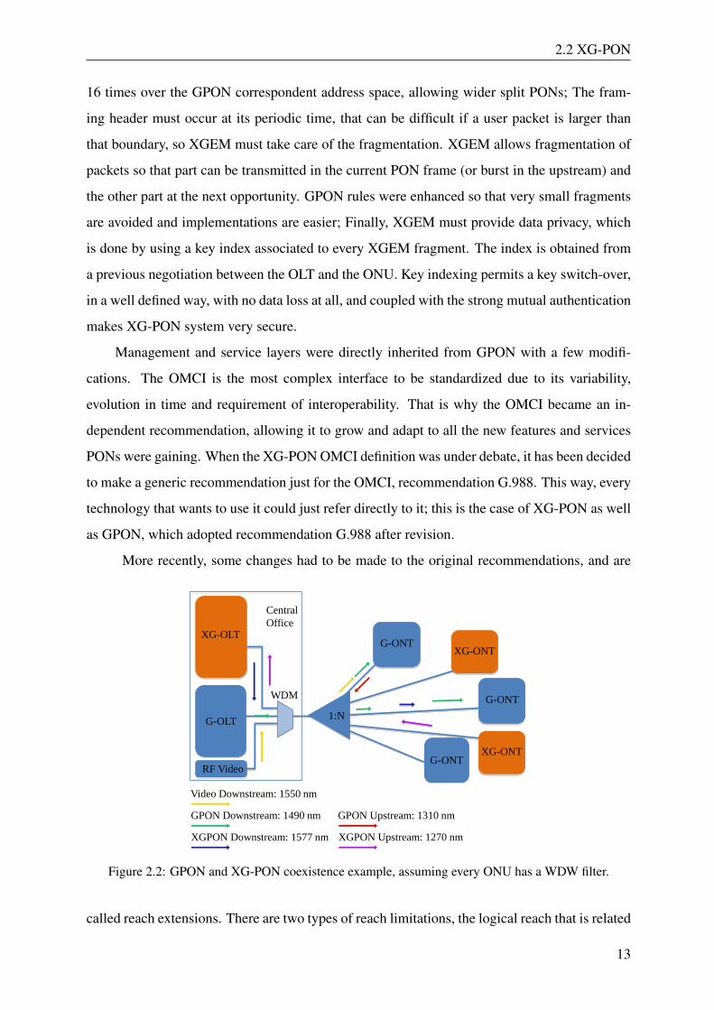
2.2 XG-PON
XG-PON was designed based on the existing GPON system, as a kind of an improvement
to the previous generation. It is defined by recommendation G.987.1. The XG-PON system
inherits: the TC layer principles; the dynamic bandwidth allocation; QoS and traffic manage-
ment; the remote operation of ONU through OMCI (redefined on G.988). This recommendation
also included improvements to the existing system, namely: enhanced power saving options;
10
2.2 XG-PON
synchronizing options enabling mobile back-hauling applications; upgrading the performance
monitoring; the optical distribution network (ODN); the security mechanisms [5].
On the PMD layer there is a difference on the downstream/upstream rate combination.
There are two standards, 10/2.5 Gbps (asymmetric) on XG-PON1 and 10/10 Gbps (symmetric)
on XG-PON2. The wavelengths chosen were 1575-1580 nm for the downstream and 1260-1280
nm for the upstream, allowing the coexistence with the previous generation and RF overlay
video [6].
GPON was class B+ (allows for loss up to 28 dB), and the coexistence of the two systems
implicates the use of a filter, which almost certainly will introduce additional loss. Also, some
deployed systems were designed with a bit more loss than required, for commercial reasons,
therefore two nominal budgets were introduced: nominal 1 that goes up to 29 dB; the nominal
2, for the over designed deployed systems, that goes up to 31 dB. In the GPON system an ex-
tended loss budget was developed that had two major features: 4 dB more loss than the nominal
budget, and ONU specifications that were unchanged from the nominal budget. After consid-
eration, the same desing features were reused in XG-PON leading to two extended budgets of
33 and 35 dB. There are no definitions on the receivers because both PIN and APD have their
specific advantages on the system. The ”decision” is left to be ruled by the market over the
years.
Although XG-PON transmission convergence (XGTC) layer is very much based on its
twin from GPON, it was more heavily structured with three distinct sub layers being defined:
the physical (PHY) adapting layer for handling issues related with the XG-PON physical layer;
the framing layer which is in charge of the PON TDMA system (the main work of the trans-
mission convergence layer); the client adaptation layer for dealing with the user signals and
carrying them over the XG-PON system.
The PHY adaptation sub-layer (PAS) deals with the low level coding in the TC frame in the
physical channel. One of the most important features is the use of FEC, required in both direc-
tions. Albeit, it can be turned off in the upstream provided that the link is good enough. There
are 24 bytes in each 125-microsecond frame reserved for a physical synchronization block in
the downstream (PSBd) destined to PAS operations such as: framing, by using the first 64 bits
with a fixed pattern, allowing the receiver to find the frame; super frame counter, occupying the
second 64 bits, providing a scrambler pre load and a much larger scale time reference; identifi-
cation of the PON, the third 64 bits are allocated for holding a value that is set by the OLT.
11
2. CHARACTERIZATION OF THE XG-PON
Traffic in the upstream direction in a PON is generally very few and as so, the upstream
is burst-transmission oriented, introducing some differences in the PSB for upstream (PSBu).
PSBu contains patterns for preamble and delimiting, with a payload that isn’t fixed size.
As for the second sub-layer, named framing sub-layer or FS, takes care of the TDMA part
of the PON, including activation and normal operation phases. XGTC has a header divided in
three parts: the first has a fix size, it contains the lengths of the other two parts and it is protected
with a header correction code (HEC); The second part is destined to carry a bandwidth map with
the several bandwidth allocations to the various ONUs on the PON; the last part contains the
PLOAM messages to the ONUs in the PON. The rest of the downstream XGTC frame is left
for the payload.
The bandwidth map concept is similarly to the GPON version, with some minor improve-
ments. As in GPON, each bandwidth allocation is for a sole ONU to transmit in upstream
and consecutive allocations can be concatenated together to improve efficiency. However, the
start-time and stop-time concept used in GPON is now dropped and replaced by a start-time
and a payload-length concept. This is an important difference since the payload-length is given
before the FEC overheads are added, facilitating the calculation of concatenated allocations
easier. Also the bandwidth allocation ID address has increased by 4 times its previous size,
allowing for wider split PONs. Moreover, there are customization possibilities since each allo-
cation specifies a burst profile. This profile includes the pattern and length of the delimiter, the
preamble and if FEC is active or not.
There are also improvements in the PLOAM messages inherited from GPON. It is now
possible to send more than one message per downstream frame, making the channel more re-
sponsive. The size of the message is increased to accommodate the known messages without
the fragmentation. Nevertheless, it were established limits to the maximum rate of each ONU
so that it will not overrun with messages. In the case of the upstream, there are two burst head-
ers: one that is fixed and contains the ONU-ID number plus the echo of the control information
from the allocation; the other is variable and carries the PLOAM message (if it exists). One
optional allocation header may exist for carrying the DBRu.
The client adaptation layer (CAS) formats the data packets to a suitable format for trans-
mission over the PON, called XG-PON encapsulation method (XGEM). Three aspects must be
dealt with: Individual flows of traffic (called ports in XG-PON) must be marked in order to be
accepted to by the right client. That is done using a 16-bit port ID, which is an increase by
12
2.2 XG-PON
16 times over the GPON correspondent address space, allowing wider split PONs; The fram-
ing header must occur at its periodic time, that can be difficult if a user packet is larger than
that boundary, so XGEM must take care of the fragmentation. XGEM allows fragmentation of
packets so that part can be transmitted in the current PON frame (or burst in the upstream) and
the other part at the next opportunity. GPON rules were enhanced so that very small fragments
are avoided and implementations are easier; Finally, XGEM must provide data privacy, which
is done by using a key index associated to every XGEM fragment. The index is obtained from
a previous negotiation between the OLT and the ONU. Key indexing permits a key switch-over,
in a well defined way, with no data loss at all, and coupled with the strong mutual authentication
makes XG-PON system very secure.
Management and service layers were directly inherited from GPON with a few modifi-
cations. The OMCI is the most complex interface to be standardized due to its variability,
evolution in time and requirement of interoperability. That is why the OMCI became an in-
dependent recommendation, allowing it to grow and adapt to all the new features and services
PONs were gaining. When the XG-PON OMCI definition was under debate, it has been decided
to make a generic recommendation just for the OMCI, recommendation G.988. This way, every
technology that wants to use it could just refer directly to it; this is the case of XG-PON as well
as GPON, which adopted recommendation G.988 after revision.
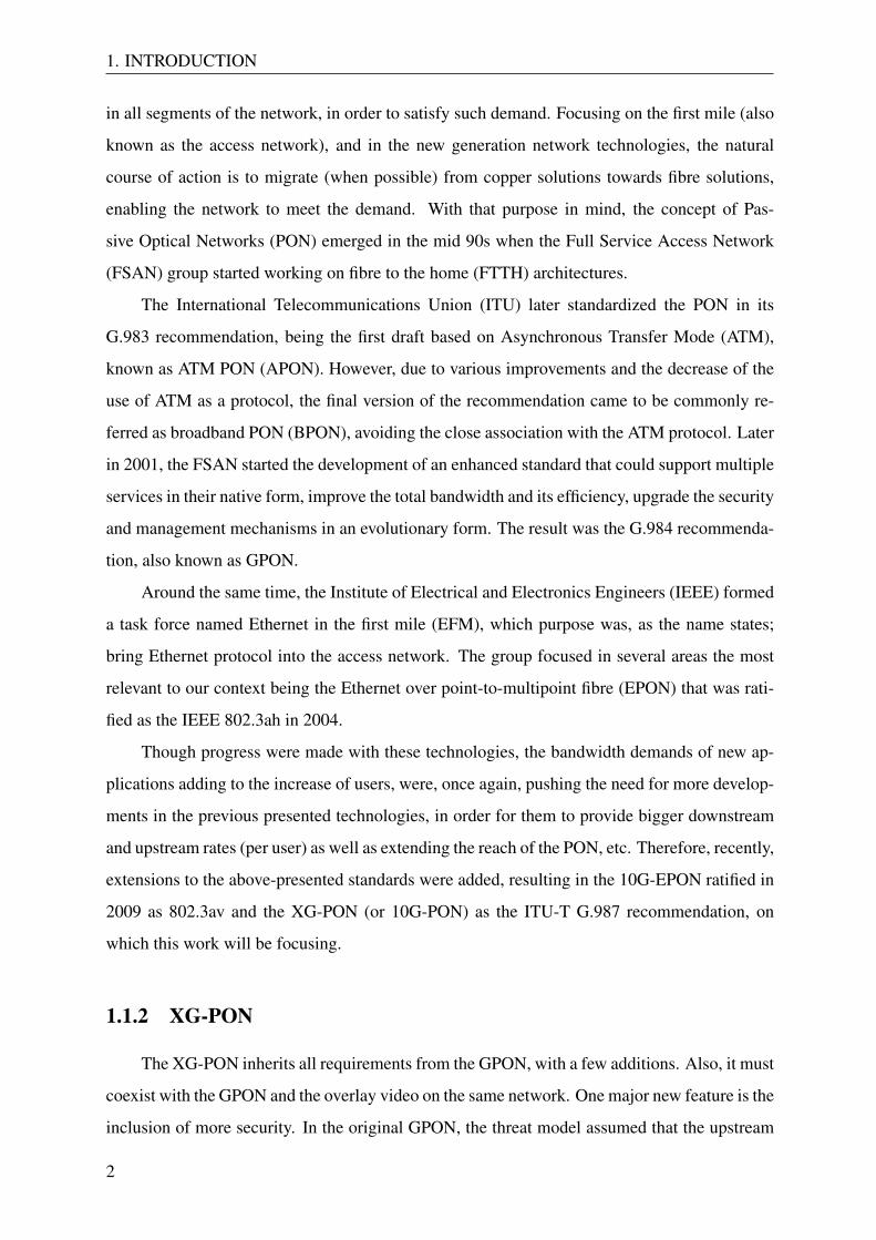
More recently, some changes had to be made to the original recommendations, and are
Video Downstream: 1550 nm
GPON Downstream: 1490 nm GPON Upstream: 1310 nm
1:N
WDM
RF Video
XGPON Upstream: 1270 nm XGPON Downstream: 1577 nm
XG-OLT
G-OLT
G-ONT
G-ONT XG-ONT
Central
Office
XG-ONT G-ONT
Figure 2.2: GPON and XG-PON coexistence example, assuming every ONU has a WDW filter.
called reach extensions. There are two types of reach limitations, the logical reach that is related
13
2. CHARACTERIZATION OF THE XG-PON
to the limits in the GTC (or XGTC) layer and the physical reach that is related with the PHY
limitations. Logically, the reach has limitations at the implementation level. The limitations are
imposed by the number of GTC (or XGTC) downstream frames that travel from the OLT to the
farthest ONU and how many BW maps the OLT has to store to properly map the corresponding
upstream frames. The logical reach of a GPON system is 60 km. On the other hand, the physical
reach is associated with the attenuation of the fibre, the loss budget and the split ratio. A GPON
system without reach extension and Class B+ transceiver may have a physical reach of 40 km
if the split ratio is 1:16. If split even further to 1:32 the reach decreases to half. It is easy to see
that the physical aspect is the bottleneck of the whole system since it imposes a shorter limit
than it should, ideally both limits should be equal. Focusing on the XG-PON system as opposed
to the GPON, the increase of rate produces a decrement in the receiver sensitivity [9], reducing
even more the physical reach. Introducing some gain in the system to achieve an optical budget
that allows the extension of reach may be a solution.
In Table 2.1, there is a summary of the GPON and XG-PON specifications and character-
istics.
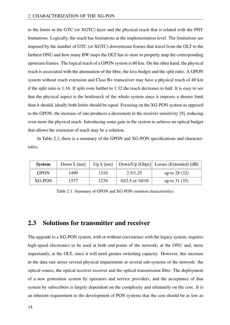
System Down λ [nm] Up λ [nm] Down/Up [Gbps] Losses (Extended) [dB]
GPON 1490 1310 2.5/1.25 up to 28 (32)
XG-PON 1577 1270 10/2.5 or 10/10 up to 31 (35)
Table 2.1: Summary of GPON and XG-PON common characteristics.
2.3 Solutions for transmitter and receiver
The upgrade to a XG-PON system, with or without coexistence with the legacy system, requires
high-speed electronics to be used at both end-points of the network; at the ONU and, more
importantly, at the OLT, since it will need greater switching capacity. However, this increase
in the data rate arises several physical impairments at several sub-systems of the network: the
optical source, the optical receiver receiver and the optical transmission fibre. The deployment
of a new generation system by operators and service providers, and the acceptance of that
system by subscribers is largely dependent on the complexity and ultimately on the cost. It is
an inherent requirement to the development of PON systems that the cost should be as low as
14
2.3 Solutions for transmitter and receiver
it can be, maintaining the solution as simple as possible. Also, it is characteristic of this kind
of system that the majority of the network cost is due to the OLT and the ONUs. Thus, a brief
overview on the transmitter and receiver components is given.
2.3.1 Receiver
The employed receivers in the XG-PON endpoints (OLT and ONU) should be able work within
the XG-PON power budget. Thus, the receivers sensitivity is a key factor. Also, they must be
able to work in the wavelengths defined by XG-PON, shown on Table 2.1.
However, the ONU is very cost sensitive, and every effort to reduce its cost must be made.
The PIN type photodetectors become more attractive in comparison with APD types since,
generally, PIN receivers are less expensive. Nevertheless, APDs are far more sensitive than
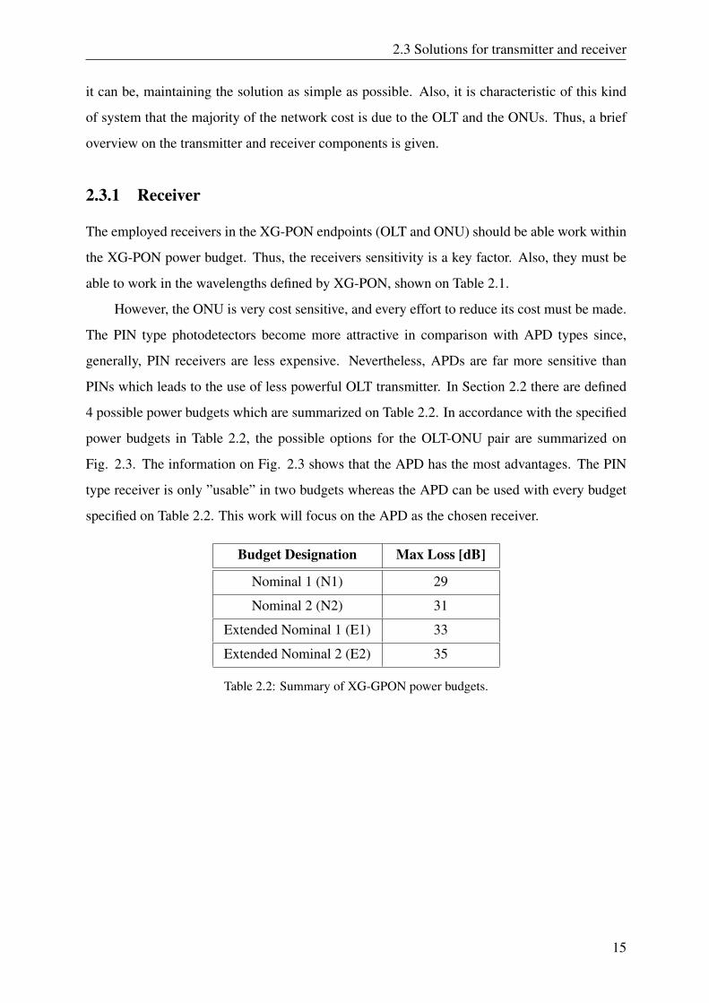
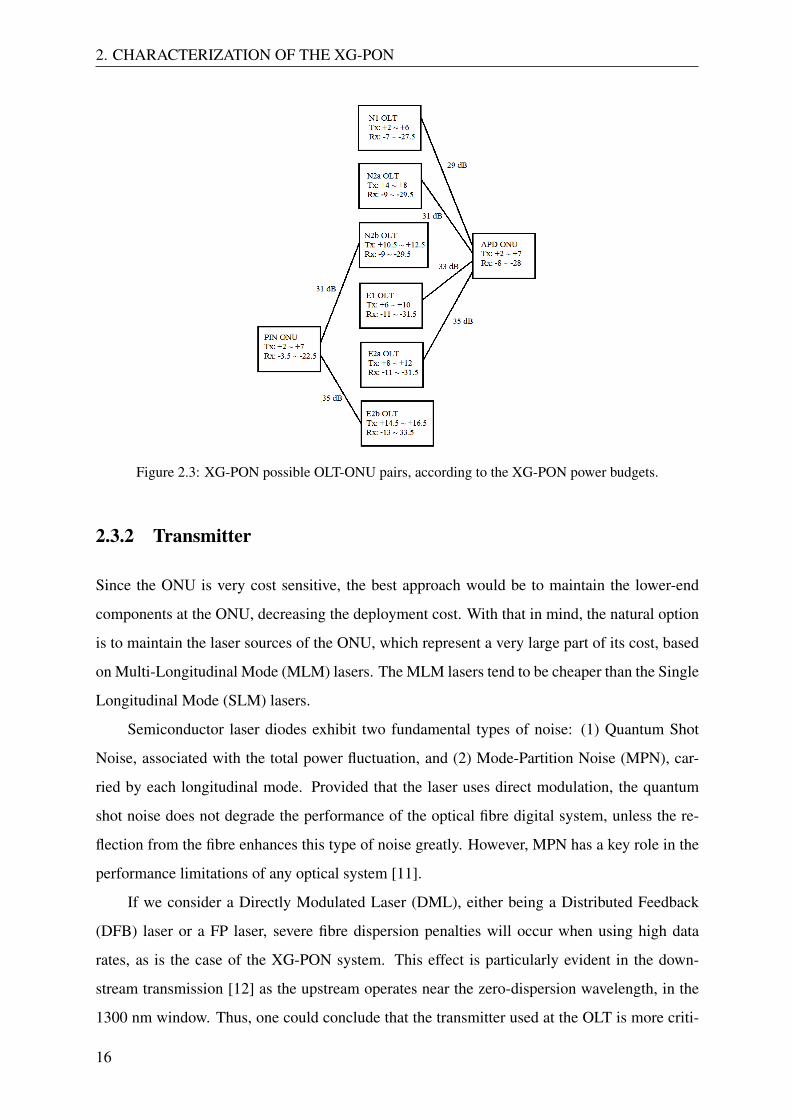
PINs which leads to the use of less powerful OLT transmitter. In Section 2.2 there are defined
4 possible power budgets which are summarized on Table 2.2. In accordance with the specified
power budgets in Table 2.2, the possible options for the OLT-ONU pair are summarized on
Fig. 2.3. The information on Fig. 2.3 shows that the APD has the most advantages. The PIN
type receiver is only ”usable” in two budgets whereas the APD can be used with every budget
specified on Table 2.2. This work will focus on the APD as the chosen receiver.
Budget Designation Max Loss [dB]
Nominal 1 (N1) 29
Nominal 2 (N2) 31
Extended Nominal 1 (E1) 33
Extended Nominal 2 (E2) 35
Table 2.2: Summary of XG-GPON power budgets.
15
2. CHARACTERIZATION OF THE XG-PON
Figure 2.3: XG-PON possible OLT-ONU pairs, according to the XG-PON power budgets.
2.3.2 Transmitter
Since the ONU is very cost sensitive, the best approach would be to maintain the lower-end
components at the ONU, decreasing the deployment cost. With that in mind, the natural option
is to maintain the laser sources of the ONU, which represent a very large part of its cost, based
on Multi-Longitudinal Mode (MLM) lasers. The MLM lasers tend to be cheaper than the Single
Longitudinal Mode (SLM) lasers.
Semiconductor laser diodes exhibit two fundamental types of noise: (1) Quantum Shot
Noise, associated with the total power fluctuation, and (2) Mode-Partition Noise (MPN), car-
ried by each longitudinal mode. Provided that the laser uses direct modulation, the quantum
shot noise does not degrade the performance of the optical fibre digital system, unless the re-
flection from the fibre enhances this type of noise greatly. However, MPN has a key role in the
performance limitations of any optical system [11].
If we consider a Directly Modulated Laser (DML), either being a Distributed Feedback
(DFB) laser or a FP laser, severe fibre dispersion penalties will occur when using high data
rates, as is the case of the XG-PON system. This effect is particularly evident in the down-
stream transmission [12] as the upstream operates near the zero-dispersion wavelength, in the
1300 nm window. Thus, one could conclude that the transmitter used at the OLT is more criti-
16
2.4 Conclusion
cal than the ONU transmitter. So, a possible configuration would be to use a MLM laser as the
ONU transmitter and a SLM laser as the OLT transmitter. This work will have more focus on
the SLM lasers.
2.4 Conclusion
In this chapter, it was presented the GPON system and its features. The XG-PON sys-
tem, which is based on the GPON was then introduced along with changes introduced by the
new standard. The different layers of the XG-PON system were presented. Furthermore, the
possibilities for the XG-PON transmitter and receiver were reviewed.
17

2. CHARACTERIZATION OF THE XG-PON
18
Chapter 3
APD impact on the system performance
In this chapter, the APD receiver modelling and characterization are presented. A motivation for
the use of this sort of optical receiver is presented in section 3.1. The theoretical principles of
APD operation are briefly explained in section 3.2, followed by the characterization of the signal
and noise in sections 3.3 and 3.5, respectively. In section 3.6, a study of the APD sensitivity
is presented. In this study, it is derived an expression for the sensitivity that can be applied
to virtually any APD receiver, regardless of the on-off keying of the input signal or the APD
receiver parameters. Also, if the common approximations and assumptions are applied to the
new sensitivity expression, this new expression results in the commonly used APD receiver
sensitivity expression. Using this new expression for the receiver sensitivity, an equation for the
optimum avalanche gain, that leads to the maximum sensitivity, is also derived and validated.
3.1 Motivation for using an APD
As explained in chapter 2, any GPON system’s optical budget becomes more critical when
higher capacity and/or reach is needed, whether it is the new XG-PON or the legacy GPON.
Furthermore, the higher rate of 10 Gbps will cause the XG-PON to be strongly affected by the
degradation of the receiver sensitivity, provided the system conditions are similar to the legacy
system. The logical step to take is to introduce gain in the system, in order to minimize the
degradation effects. Also, it is desirable to enable the most affordable network provisioning
through minimization of the cost of network components. Preferably, changing the components
at the OLT allowing for the associated cost be shared by all ONUs in the network.
The gain introduction can be accomplished by using optical amplification in the terminal
elements of the network or replace the employed optical receiver PIN photo-diode by an APD
19
3. APD IMPACT ON THE SYSTEM PERFORMANCE
optical receiver, a photo-diode with gain.
However, the gain introduced by the APD is limited due to the classic noise and gain trade-
off [13]. Nevertheless, a considerable amount of effort has been done to determine the optimum
gain conditions in order to achieve the maximum receiver sensitivity [14].
3.2 Principles of APDs
The APD photo-diodes are a type of optical receiver that have the special property of providing
a built-in first stage of gain through the avalanche multiplication. They internally multiply the
primary photo-current before the following circuitry. The sensitivity increase happens since the
multiplication occurs before the photo-current encounter the thermal noise associated with the
receiver circuit. For the carrier multiplication to take place, the photo-generated carriers must
transverse a region where a very high electric field is present (as shown in Fig. 3.1). In this
high-field region, a photo-generated electron or hole can gain enough energy so that it ionizes
bound electrons in the valence band upon colliding with them. The newly created carriers are
also accelerated by the high electric field, thus gaining enough energy to cause further impact
ionization. This phenomenon is the avalanche effect [15].
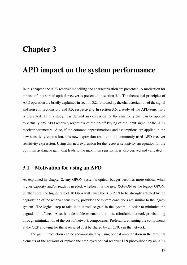
Figure 3.1: Avalanche photo-diode reach-through schematic.
In order to achieve carrier multiplication with very little excess noise, it is commonly used
a reach-through structure (Fig. 3.1), which is composed by high-resistivity p-type material,
(material with a larger concentration of holes than electrons), deposited as an epitaxial layer on
a p` substrate [15]. A p-type diffusion is then made in the high-resistivity material, followed
by the construction of an n` layer, (layer of a material with a higher concentration of electron
20
3.3 Signal characterization
than holes). The nearly intrinsic π layer is simply an intrinsic material that inadvertently has
some p doping because of imperfect purification.
After entering the device through the p` region, light is absorbed in the π material, which
will collect the carriers that are photo-generated. This absorption will cause electron-holes
pair to appear, which will be separated due to the electric field in that region. The photo-
generated electrons will then move within this region, acquiring enough energy to generate a
new electron-hole pair. The energetic electron transfers part of its kinetic energy to another
electron in the valance band releasing it, leaving behind a hole. Thus, a single primary electron,
generated through absorption of a photon, creates many secondary electrons and holes, all of
which contribute to the photo-diode current. Similarly, the primary hole can also generate
secondary electron-hole pairs, contributing to the current. The generation rate is governed by
two parameters, α and β, the impact-ionization coefficients of electrons and holes, respectively.
These coefficients typically vary from one material to another.
It is called to the average number of electron-hole pairs created by carrier, per unit of
distance travelled, the ionization rate, represented by kA. The ionization rate is the ratio between
the holes and electrons impact-ionization coefficients. In practice, the APD performance is
better when the avalanche process is dominated by one charge ( α" β or β" α) [14].
3.3 Signal characterization
Let the value of the total multiplied output current be Imc and Ip the primary unmultiplied cur-
rent. Then, we may define the multiplication factor M for all carriers generated in the APD
as
M “Imc
Ip. (3.1)
The value of M is expressed as an average quantity due to the avalanche mechanism being a
statistical process; every diode carrier pair generated experiences a different multiplication.
Current gains differ from wavelength to wavelength. That dependence is attributed to
the mixed initiation of the avalanche process by holes and electrons when most of the light
is absorbed close to the detector surface, in the n`p region. This effect is more evident when
using short wavelengths where a major part of the optical power is absorbed close to the surface,
contrarily to what happens with longer wavelengths [15].
21
3. APD IMPACT ON THE SYSTEM PERFORMANCE
The optical receiver depend upon a minimum of current (Ip) to operate reliably, which is
the same to say that a minimum amount of power (pi) is needed for achieving that current. This
correlation is translated in expression 3.2, where Rλ corresponds to the unity gain responsivity.
pi “Ip
Rλ
(3.2)
So, the performance of an APD is also characterized by its responsivity, which is given by
expression 3.3 where η corresponds to the quantum efficiency, q is the electron charge, h is the
Planck’s constant and ν is the operating frequency of the optical signal.
RλAPD “ηqhν
M “ RλM (3.3)
Given the correlation between the minimum received power and the minimum current, detectors
with large responsivity are preferred since they minimize the optical power needed.
The received power is a combination of the power when the light source is off (bit 0),
commonly defined as pi,0, and the power when the light source is on (bit 1), known as pi,1.
In optical communications, for characterizing the signal it is also used a quantity named the
extinction ratio. This ratio, represented by r, is defined as quotient of the power of the bit 0 and
the power of the bit 1 as follows
r “pi,0
pi,1(3.4)
where 0 ď r ă 1. Nevertheless, ITU-T established that the maximum value of the extinction
ratio that can be used is r “ 0.152 [17]. The extinction ratio can also be represented as
Rext “pi,1
pi,0. (3.5)
Expression 3.5 is useful for representing the extinction ratio in dB, and the corresponding de-
fined limit is a minimum of 8.2 dB.
3.4 Receiver characterization
The optical receiver is responsible for converting the signals from the optical domain into the
electric domain and processing the resulting electric signal. There are optical receivers with
optical pre-amplification, which consists in using an optical amplifier before the optic-electric
22
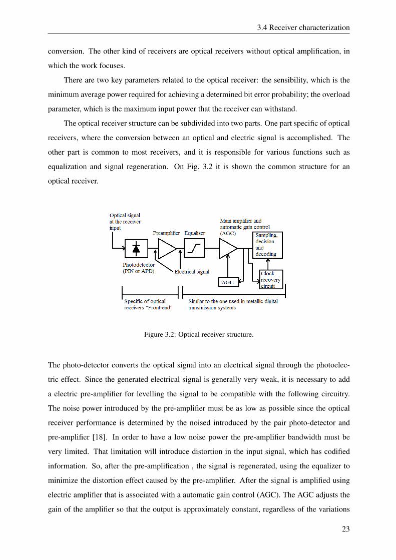
3.4 Receiver characterization
conversion. The other kind of receivers are optical receivers without optical amplification, in
which the work focuses.
There are two key parameters related to the optical receiver: the sensibility, which is the
minimum average power required for achieving a determined bit error probability; the overload
parameter, which is the maximum input power that the receiver can withstand.
The optical receiver structure can be subdivided into two parts. One part specific of optical
receivers, where the conversion between an optical and electric signal is accomplished. The
other part is common to most receivers, and it is responsible for various functions such as
equalization and signal regeneration. On Fig. 3.2 it is shown the common structure for an
optical receiver.
Figure 3.2: Optical receiver structure.
The photo-detector converts the optical signal into an electrical signal through the photoelec-
tric effect. Since the generated electrical signal is generally very weak, it is necessary to add
a electric pre-amplifier for levelling the signal to be compatible with the following circuitry.
The noise power introduced by the pre-amplifier must be as low as possible since the optical
receiver performance is determined by the noised introduced by the pair photo-detector and
pre-amplifier [18]. In order to have a low noise power the pre-amplifier bandwidth must be
very limited. That limitation will introduce distortion in the input signal, which has codified
information. So, after the pre-amplification , the signal is regenerated, using the equalizer to
minimize the distortion effect caused by the pre-amplifier. After the signal is amplified using
electric amplifier that is associated with a automatic gain control (AGC). The AGC adjusts the
gain of the amplifier so that the output is approximately constant, regardless of the variations
23

3. APD IMPACT ON THE SYSTEM PERFORMANCE
in the input. The sampling and decision circuitry, which is synced by the clock signal from the
clock extraction circuitry, is then used to decode the signal.
The commonly used photo-detectors in optical fibre transmission systems are semiconduc-
tor photo-diodes. The most used types of photo-diodes are the PIN or the APD, in which this
work focuses.
3.5 Noise characterization
The main function of optical receivers is to convert the incident optical power pi into an elec-
trical current. In Eq. 3.2 it is assumed that the conversion is noise free, which is not true in
practice. There are two main noise mechanisms that lead to fluctuations in the current regard-
less of the incident optical signal having a constant power, the shot noise and the thermal noise.
In that way, Eq. 3.2 remains valid only if Ip is interpreted as the average current.
3.5.1 Thermal noise
At normal temperatures, higher than zero Kelvin, electrons will move randomly in any con-
ductor. This motion in a resistor manifests as a fluctuating current even in the absence of an
applied voltage. The load resistor RL in the front end of an optical receiver [19] will add these
fluctuations to the current generated by the photo-diode. Thus, this additional power component
is called the thermal noise, and it is represented by its variance σ2c given by
σ2c “ p4kBT{RLqFnBe,n (3.6)
where Fn represents the factor by which thermal noise is enhanced by the various resistors used
in pre and main amplifiers, Be,n is the effective noise bandwidth, the bandwidth of noise in hertz
over which the noise is considered, T is the temperature, and kB is the Boltzmann constant.
This noise is exactly the same in both PIN and APD, it does not depend on the photo-diode type
since it originates in the electrical components of the receiver.
3.5.2 Shot noise
The shot noise is a manifestation of the fact that an electrical current consists of a stream of
electrons generated at random times. As deducted in [19], the shot noise variance σ2s is defined
24
3.5 Noise characterization
by
σ2s “ 2qpIp` IdqBe,n (3.7)
where Id is the dark current, a current representing the constant response exhibited by a receiver
when not actively being exposed to light. However, in the case of the APD, the generation of
secondary electron-hole pairs at random times through the process of impact ionization, from
where the APD gain results are obtained, adds a contribution to the primary electron-hole pairs
associated shot noise. In fact, the multiplication factor is itself a random variable, being M the
average APD gain. Applying these considerations in Eq. 3.7 translates into [15]
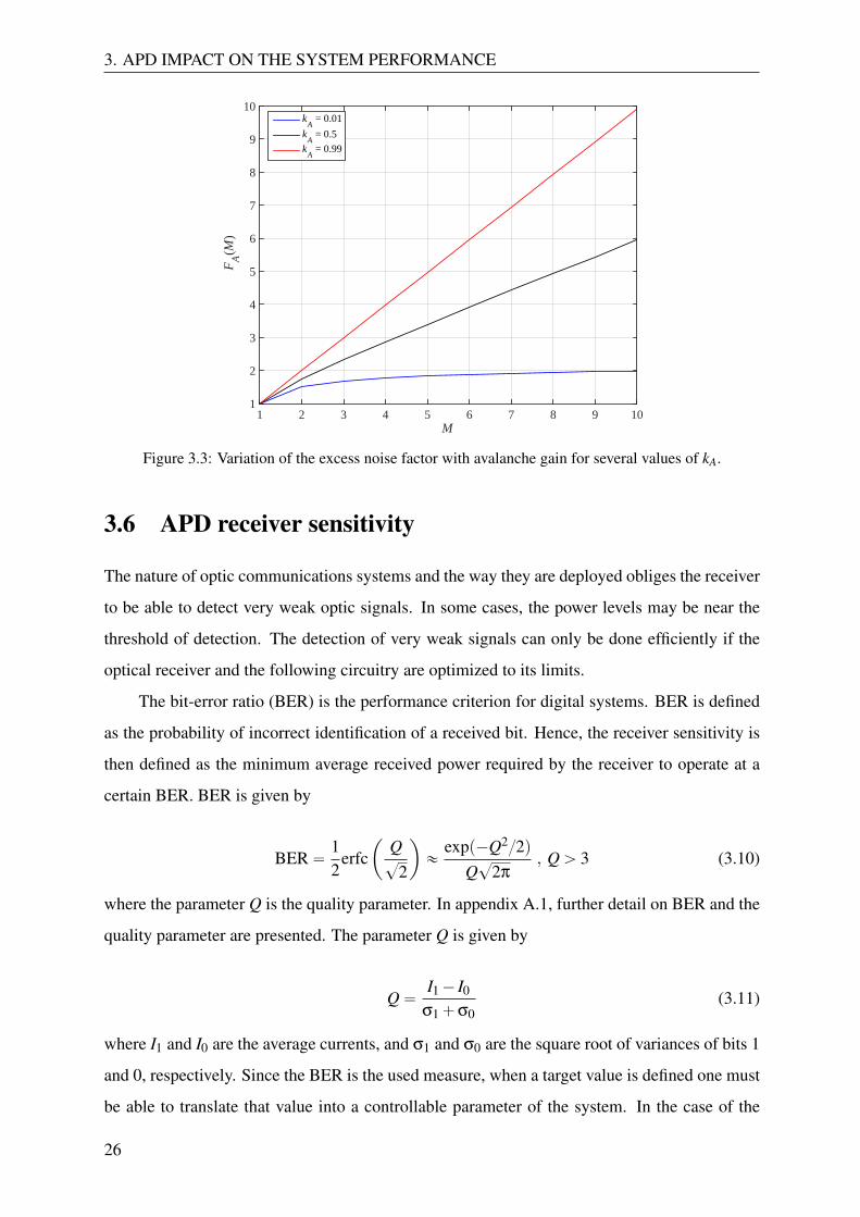
σ2s “ 2qM2FApMqpRλ pi` IdqBe,n. (3.8)
In expression 3.8 FApMq is the excess noise factor of the APD, a factor that represents yet
another source of noise that describes the statistical noise inherent to the stochastic APD multi-
plication process. It is given by
FApMq “ kAM`p1´ kAqp2´1{Mq. (3.9)
The symbol kA in Eq. 3.9 represents the ionization coefficient ratio for the APD, which in
general increases with M and is in the range 0 ă kA ă 1. This value should be as small as
possible in order to achieve the best performance from an APD [16]. In the case of an PIN
receiver, M “ 1 which makes FApMq “ kA`1´ kA “ 1.
The simple plot of Eq. 3.9, as shown in Fig. 3.3, shows that the value of FApMq varies
between 2 and M, approximately. This confirms that lower values of kA lead to lower values of
excess noise factor. The mathematical result shown on Fig. 3.3 is explained physically by the
phenomenon quantified by the ionization rate kA. As stated in section 3.2, the ionization rate is
the ratio between the impact-ionization coefficients of holes and electrons, β and α, respectively.
Though, this dimensionless parameter is defined in two different ways, as kA “ β{α if α" β or
as kA “ α{β if β " α [14]. So, in either case, the greater the dominance of one charge over the
other in the avalanche process, the lower the ionization rate coefficient will be. Thus, based on
the statement in section 3.2 that dominance of one charge over the other is better in practice for
APD performance, lower values of ionization rate kA, lead to better APD performance.
25
3. APD IMPACT ON THE SYSTEM PERFORMANCE
M1 2 3 4 5 6 7 8 9 10
FA
(M)
1
2
3
4
5
6
7
8
9
10k
A = 0.01
kA = 0.5
kA = 0.99
Figure 3.3: Variation of the excess noise factor with avalanche gain for several values of kA.
3.6 APD receiver sensitivity
The nature of optic communications systems and the way they are deployed obliges the receiver
to be able to detect very weak optic signals. In some cases, the power levels may be near the
threshold of detection. The detection of very weak signals can only be done efficiently if the
optical receiver and the following circuitry are optimized to its limits.
The bit-error ratio (BER) is the performance criterion for digital systems. BER is defined
as the probability of incorrect identification of a received bit. Hence, the receiver sensitivity is
then defined as the minimum average received power required by the receiver to operate at a
certain BER. BER is given by
BER“12
erfcˆ
Q?
2
˙
«expp´Q2{2q
Q?
2π, Qą 3 (3.10)
where the parameter Q is the quality parameter. In appendix A.1, further detail on BER and the
quality parameter are presented. The parameter Q is given by
Q“I1´ I0
σ1`σ0(3.11)
where I1 and I0 are the average currents, and σ1 and σ0 are the square root of variances of bits 1
and 0, respectively. Since the BER is the used measure, when a target value is defined one must
be able to translate that value into a controllable parameter of the system. In the case of the
26
3.6 APD receiver sensitivity
optical receiver, this manageable parameter is the average incident optical power. In order to
relate the BER to the average incident power some analytical development must be performed.
In the denominator part of Eq. 3.11, there are the square root of variances of bits 0 and 1,
which are defined by
σ0 “
c
´
σ2s,0`σ2
c
¯
(3.12)
σ1 “
c
´
σ2s,1`σ2
c
¯
. (3.13)
From Eqs. 3.12 and 3.13, one can conclude that the square root variance of a given bit is
composed by the thermal noise contribution and the related bit shot noise contribution. Using
expression 3.8, the shot noise variance for bits 0 and 1 can be expressed in terms of their average
powers, pi,0 and pi,1, respectively, as follows
σ2s,0,1 “ 2qM2FApMqpRλ pi,0,1` IdqBe,n. (3.14)
where the average power pi,0 is then defined as
pi,0 “2pirp1` rq
, (3.15)
and pi,1 can be related to the total average power as
pi,1 “2pi
p1` rq. (3.16)
The numerator part of Eq. 3.11 is composed by the subtraction of the average currents of bit
1 and 0. Using Eqs. 3.2 and 3.3, the average currents of bit 1 and 0 can be related to their
corresponding powers, pi,1 and pi,0, respectively. Relating again the extinction ratio with the
average powers of bits 0 and 1, (see appendix A.2 for further details), an expression for the
subtraction of the currents in function of the total average incident power pi is obtained
I1´ I0 “MRλ
„
2pi
p1` rq´
2pirp1` rq
. (3.17)
Now, since all parts of Eq. 3.11 can be expressed in terms of pi, resolving the equation in
order to pi will lead to an expression where Q is a variable parameter in that expression. With
such an expression, one can define the target BER and obtain the corresponding Q value. Then,
27
3. APD IMPACT ON THE SYSTEM PERFORMANCE
replace that value on the pi expression and obtain the minimum average incident power that
complies to that BER target. This minimum power value is called the sensitivity.
Appendix A.3 details the equation analytical developments and considerations which re-
sulted in the sensitivity expression for an APD with non-null extinction ratio, given by
pi “Qpr`1q
MRλpr´1q2
„
QqFApMqMBe,npr`1q
`
b
p2qFApMqM2Be,nId`σ2cqpr´1q2` rp2QqFApMqMBe,nq2
.
(3.18)
The sensitivity pi depends on several optical receiver parameters, such as the receiver effective
bandwidth Be,n, the thermal noise variance σ2c , the responsivity Rλ. The dependency of the
receiver sensitivity on the avalanche gain is both direct, since expression 3.18 depends on M, and
indirect through the excess noise factor FA. This indicates that there will be a trade-off between
the gain value and the consequent introduced noise. The incident optical signal characteristics
dependency is represented by the extinction ratio r. Finally, as wanted, it depends on the Q
parameter, which is directly related with BER through Eq. 3.10.
The sensitivity expression 3.18 was derived for the APD receiver. However, it can be
applied to the PIN receiver by considering the PIN as an APD with unitary gain (M “ 1).
If one considers the simple case of a null extinction ratio (r “ 0), and also neglect the
contribution from the dark current (Id “ 0), the well known expression presented in [19] is
obtained
pi “QRλ
´
qFApMqQBe,n`σc
M
¯
. (3.19)
3.7 APD improvement over PIN
The improvement in the receiver sensitivity obtained by using an APD instead of a PIN can be
estimated by comparing the expression 3.18 and its version for a PIN diode (M “ 1). For a PIN,
the sensitivity expression 3.18 results in
piPIN “Qpr`1q
Rλpr´1q2
„
QqBe,npr`1q`b
p2qBe,nId`σ2cqpr´1q2` rp2QqBe,nq2
. (3.20)
28
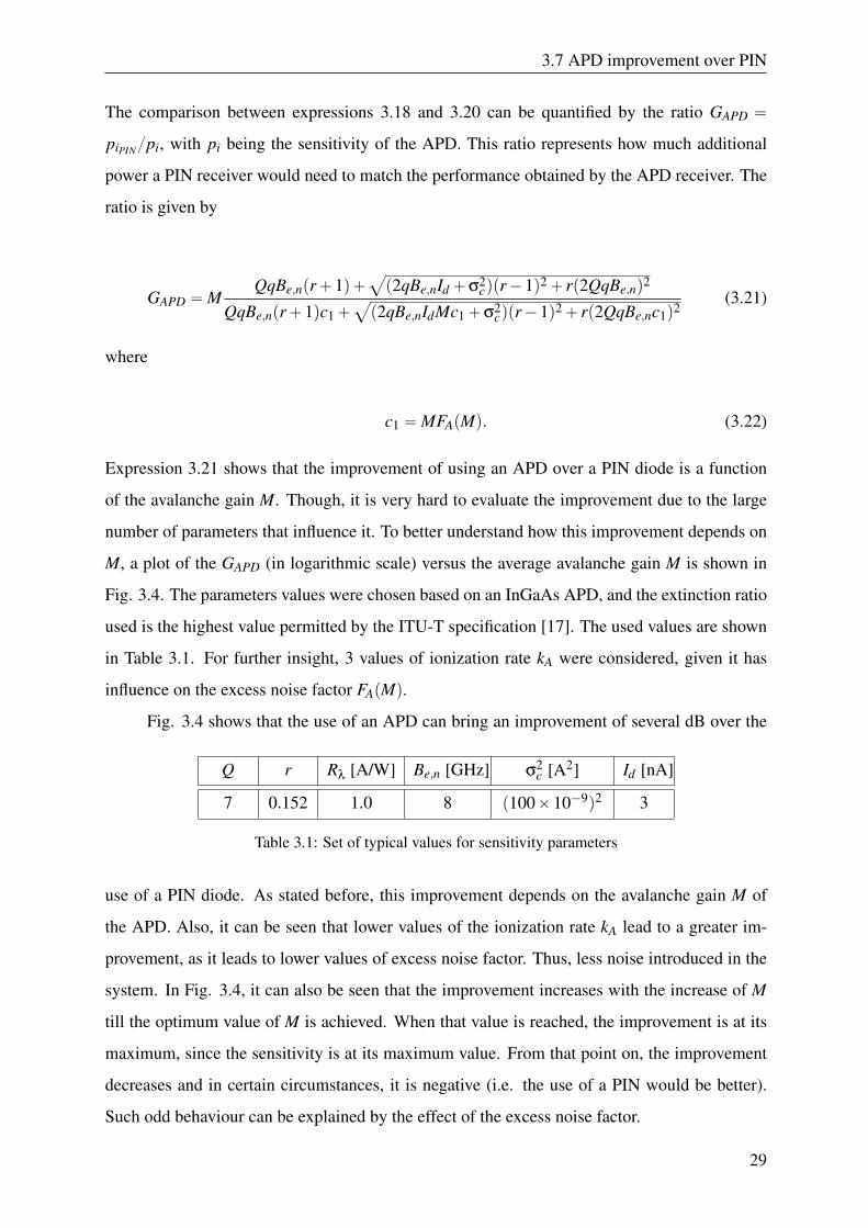
3.7 APD improvement over PIN
The comparison between expressions 3.18 and 3.20 can be quantified by the ratio GAPD “
piPIN{pi, with pi being the sensitivity of the APD. This ratio represents how much additional
power a PIN receiver would need to match the performance obtained by the APD receiver. The
ratio is given by
GAPD “MQqBe,npr`1q`
a
p2qBe,nId`σ2cqpr´1q2` rp2QqBe,nq2
QqBe,npr`1qc1`a
p2qBe,nIdMc1`σ2cqpr´1q2` rp2QqBe,nc1q2
(3.21)
where
c1 “MFApMq. (3.22)
Expression 3.21 shows that the improvement of using an APD over a PIN diode is a function
of the avalanche gain M. Though, it is very hard to evaluate the improvement due to the large
number of parameters that influence it. To better understand how this improvement depends on
M, a plot of the GAPD (in logarithmic scale) versus the average avalanche gain M is shown in
Fig. 3.4. The parameters values were chosen based on an InGaAs APD, and the extinction ratio
used is the highest value permitted by the ITU-T specification [17]. The used values are shown
in Table 3.1. For further insight, 3 values of ionization rate kA were considered, given it has
influence on the excess noise factor FApMq.
Fig. 3.4 shows that the use of an APD can bring an improvement of several dB over the
Q r Rλ [A/W] Be,n [GHz] σ2c [A2] Id [nA]
7 0.152 1.0 8 p100ˆ10´9q2 3
Table 3.1: Set of typical values for sensitivity parameters
use of a PIN diode. As stated before, this improvement depends on the avalanche gain M of
the APD. Also, it can be seen that lower values of the ionization rate kA lead to a greater im-
provement, as it leads to lower values of excess noise factor. Thus, less noise introduced in the
system. In Fig. 3.4, it can also be seen that the improvement increases with the increase of M
till the optimum value of M is achieved. When that value is reached, the improvement is at its
maximum, since the sensitivity is at its maximum value. From that point on, the improvement
decreases and in certain circumstances, it is negative (i.e. the use of a PIN would be better).
Such odd behaviour can be explained by the effect of the excess noise factor.
29
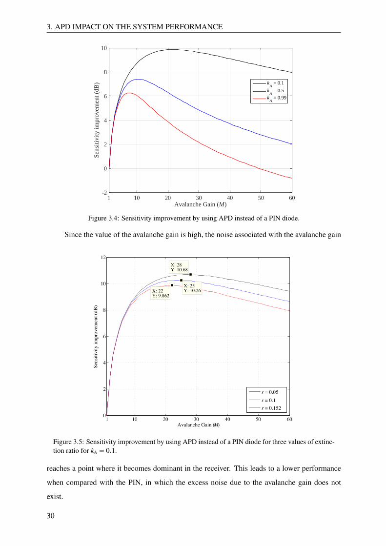
3. APD IMPACT ON THE SYSTEM PERFORMANCE
Avalanche Gain (M)1 10 20 30 40 50 60
Sens
itivi
ty im
prov
emen
t (dB
)
-2
0
2
4
6
8
10
kA
= 0.1
kA
= 0.5
kA
= 0.99
Figure 3.4: Sensitivity improvement by using APD instead of a PIN diode.
Since the value of the avalanche gain is high, the noise associated with the avalanche gain
1 10 20 30 40 50 600
2
4
6
8
10
12
X: 22Y: 9.862
X: 25Y: 10.26
X: 28Y: 10.68
Avalanche Gain (M)
Sens
itivi
ty im
prov
emen
t (dB
)
r = 0.05r = 0.1r = 0.152
Figure 3.5: Sensitivity improvement by using APD instead of a PIN diode for three values of extinc-tion ratio for kA “ 0.1.
reaches a point where it becomes dominant in the receiver. This leads to a lower performance
when compared with the PIN, in which the excess noise due to the avalanche gain does not
exist.
30
3.7 APD improvement over PIN
The result shown in Fig. 3.4 allows for an analysis on how the ionization rate kA influences
the optimum gain of the APD. Again, the result confirms the conclusion of section 3.5.2 which
stated that lower values of ionization rate kA lead to better APD performance. Though, this
result also shows that lower values of ionization rate allow for a more stable performance, less
sensitive to minor changes in the optical receiver parameters, since the variation of the perfor-
mance around the optimum gain is smaller in lower values of ionization rate.
The result shown in Fig. 3.4 does not show the influence that the extinction ratio has on
1 10 20 30 40 50
1
2
3
4
5
6
7
8
9
X: 10Y: 7.402
X: 11Y: 7.727
X: 13Y: 8.071
Avalanche Gain (M)
Sens
itivi
ty im
prov
emen
t (dB
)
r = 0.05r = 0.1r = 0.152
Figure 3.6: Sensitivity improvement by using APD instead of a PIN diode for three values of extinc-tion ratio for kA “ 0.5.
the performance improvement. In order to show the extinction ratio influence, the improvement
plot was redone, with three extinction ratio values, r “ 0.05, r “ 0.1 and r “ 0.152, for each of
the ionization rates used in Fig. 3.4 . The plots are shown in figures 3.5, 3.6 and 3.7 , for values
of ionization rate kA “ 0.1, kA “ 0.5 and kA “ 1.0, respectively.
The extinction ratio decreases the APD improvement. The higher the extinction ratio, the
lower the improvement. Nevertheless, the extinction ratio influence is low when compared with
the ionization rate influence. The extinction ratio has impact on the improvement value, how-
ever it does not affect the ”stability” of that improvement. Thus, it can be concluded that when
designing an optical transmission system, the ionization rate is a much more critical parameter
than the extinction ratio.
31
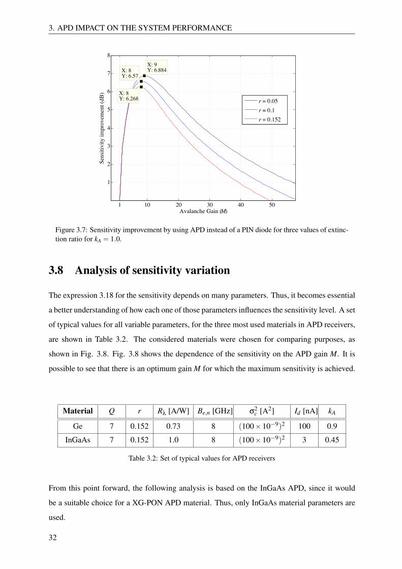
3. APD IMPACT ON THE SYSTEM PERFORMANCE
1 10 20 30 40 50
1
2
3
4
5
6
7
8
X: 8Y: 6.57
X: 8Y: 6.268
X: 9Y: 6.884
Avalanche Gain (M)
Sens
itivi
ty im
prov
emen
t (dB
)r = 0.05r = 0.1r = 0.152
Figure 3.7: Sensitivity improvement by using APD instead of a PIN diode for three values of extinc-tion ratio for kA “ 1.0.
3.8 Analysis of sensitivity variation
The expression 3.18 for the sensitivity depends on many parameters. Thus, it becomes essential
a better understanding of how each one of those parameters influences the sensitivity level. A set
of typical values for all variable parameters, for the three most used materials in APD receivers,
are shown in Table 3.2. The considered materials were chosen for comparing purposes, as
shown in Fig. 3.8. Fig. 3.8 shows the dependence of the sensitivity on the APD gain M. It is
possible to see that there is an optimum gain M for which the maximum sensitivity is achieved.
Material Q r Rλ [A/W] Be,n [GHz] σ2c [A2] Id [nA] kA
Ge 7 0.152 0.73 8 p100ˆ10´9q2 100 0.9
InGaAs 7 0.152 1.0 8 p100ˆ10´9q2 3 0.45
Table 3.2: Set of typical values for APD receivers
From this point forward, the following analysis is based on the InGaAs APD, since it would
be a suitable choice for a XG-PON APD material. Thus, only InGaAs material parameters are
used.
32
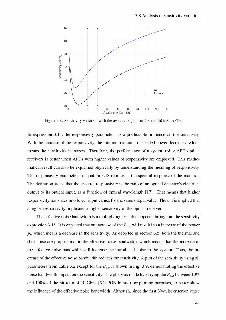
3.8 Analysis of sensitivity variation
Avalanche Gain (M)0 10 20 30 40 50 60 70 80 90 100
Sens
itivi
ty (
dBm
)
-28
-26
-24
-22
-20
-18
-16
GeInGaAs
Figure 3.8: Sensitivity variation with the avalanche gain for Ge and InGaAs APDs.
In expression 3.18, the responsivity parameter has a predictable influence on the sensitivity.
With the increase of the responsivity, the minimum amount of needed power decreases, which
means the sensitivity increases. Therefore, the performance of a system using APD optical
receivers is better when APDs with higher values of responsivity are employed. This mathe-
matical result can also be explained physically by understanding the meaning of responsivity.
The responsivity parameter in equation 3.18 represents the spectral response of the material.
The definition states that the spectral responsivity is the ratio of an optical detector’s electrical
output to its optical input, as a function of optical wavelength [17]. That means that higher
responsivity translates into lower input values for the same output value. Thus, it is implied that
a higher responsivity implicates a higher sensitivity of the optical receiver.
The effective noise bandwidth is a multiplying term that appears throughout the sensitivity
expression 3.18. It is expected that an increase of the Be,n will result in an increase of the power
pi, which means a decrease in the sensitivity. As depicted in section 3.5, both the thermal and
shot noise are proportional to the effective noise bandwidth, which means that the increase of
the effective noise bandwidth will increase the introduced noise in the system. Thus, the in-
crease of the effective noise bandwidth reduces the sensitivity. A plot of the sensitivity using all
parameters from Table 3.2 except for the Be,n is shown in Fig. 3.9, demonstrating the effective
noise bandwidth impact on the sensitivity. The plot was made by varying the Be,n between 10%
and 100% of the bit ratio of 10 Gbps (XG-PON bitrate) for plotting purposes, to better show
the influence of the effective noise bandwidth. Although, since the first Nyquist criterion states
33
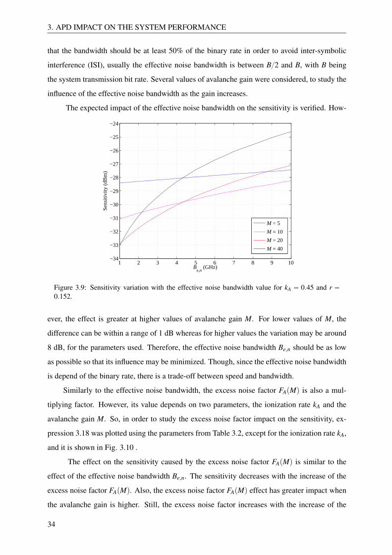
3. APD IMPACT ON THE SYSTEM PERFORMANCE
that the bandwidth should be at least 50% of the binary rate in order to avoid inter-symbolic
interference (ISI), usually the effective noise bandwidth is between B{2 and B, with B being
the system transmission bit rate. Several values of avalanche gain were considered, to study the
influence of the effective noise bandwidth as the gain increases.
The expected impact of the effective noise bandwidth on the sensitivity is verified. How-
1 2 3 4 5 6 7 8 9 10−34
−33
−32
−31
−30
−29
−28
−27
−26
−25
−24
Be,n
(GHz)
Sen
sitiv
ity (
dBm
)
M = 5
M = 10
M = 20
M = 40
Figure 3.9: Sensitivity variation with the effective noise bandwidth value for kA “ 0.45 and r “0.152.
ever, the effect is greater at higher values of avalanche gain M. For lower values of M, the
difference can be within a range of 1 dB whereas for higher values the variation may be around
8 dB, for the parameters used. Therefore, the effective noise bandwidth Be,n should be as low
as possible so that its influence may be minimized. Though, since the effective noise bandwidth
is depend of the binary rate, there is a trade-off between speed and bandwidth.
Similarly to the effective noise bandwidth, the excess noise factor FApMq is also a mul-
tiplying factor. However, its value depends on two parameters, the ionization rate kA and the
avalanche gain M. So, in order to study the excess noise factor impact on the sensitivity, ex-
pression 3.18 was plotted using the parameters from Table 3.2, except for the ionization rate kA,
and it is shown in Fig. 3.10 .
The effect on the sensitivity caused by the excess noise factor FApMq is similar to the
effect of the effective noise bandwidth Be,n. The sensitivity decreases with the increase of the
excess noise factor FApMq. Also, the excess noise factor FApMq effect has greater impact when
the avalanche gain is higher. Still, the excess noise factor increases with the increase of the
34
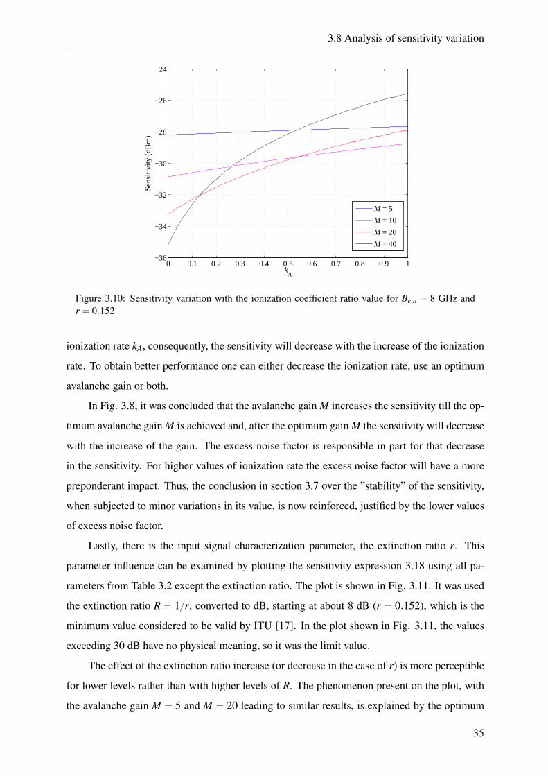
3.8 Analysis of sensitivity variation
0 0.1 0.2 0.3 0.4 0.5 0.6 0.7 0.8 0.9 1−36
−34
−32
−30
−28
−26
−24
kA
Sen
sitiv
ity (
dBm
)
M = 5
M = 10
M = 20
M = 40
Figure 3.10: Sensitivity variation with the ionization coefficient ratio value for Be,n “ 8 GHz andr “ 0.152.
ionization rate kA, consequently, the sensitivity will decrease with the increase of the ionization
rate. To obtain better performance one can either decrease the ionization rate, use an optimum
avalanche gain or both.
In Fig. 3.8, it was concluded that the avalanche gain M increases the sensitivity till the op-
timum avalanche gain M is achieved and, after the optimum gain M the sensitivity will decrease
with the increase of the gain. The excess noise factor is responsible in part for that decrease
in the sensitivity. For higher values of ionization rate the excess noise factor will have a more
preponderant impact. Thus, the conclusion in section 3.7 over the ”stability” of the sensitivity,
when subjected to minor variations in its value, is now reinforced, justified by the lower values
of excess noise factor.
Lastly, there is the input signal characterization parameter, the extinction ratio r. This
parameter influence can be examined by plotting the sensitivity expression 3.18 using all pa-
rameters from Table 3.2 except the extinction ratio. The plot is shown in Fig. 3.11. It was used
the extinction ratio R “ 1{r, converted to dB, starting at about 8 dB (r “ 0.152), which is the
minimum value considered to be valid by ITU [17]. In the plot shown in Fig. 3.11, the values
exceeding 30 dB have no physical meaning, so it was the limit value.
The effect of the extinction ratio increase (or decrease in the case of r) is more perceptible
for lower levels rather than with higher levels of R. The phenomenon present on the plot, with
the avalanche gain M “ 5 and M “ 20 leading to similar results, is explained by the optimum
35
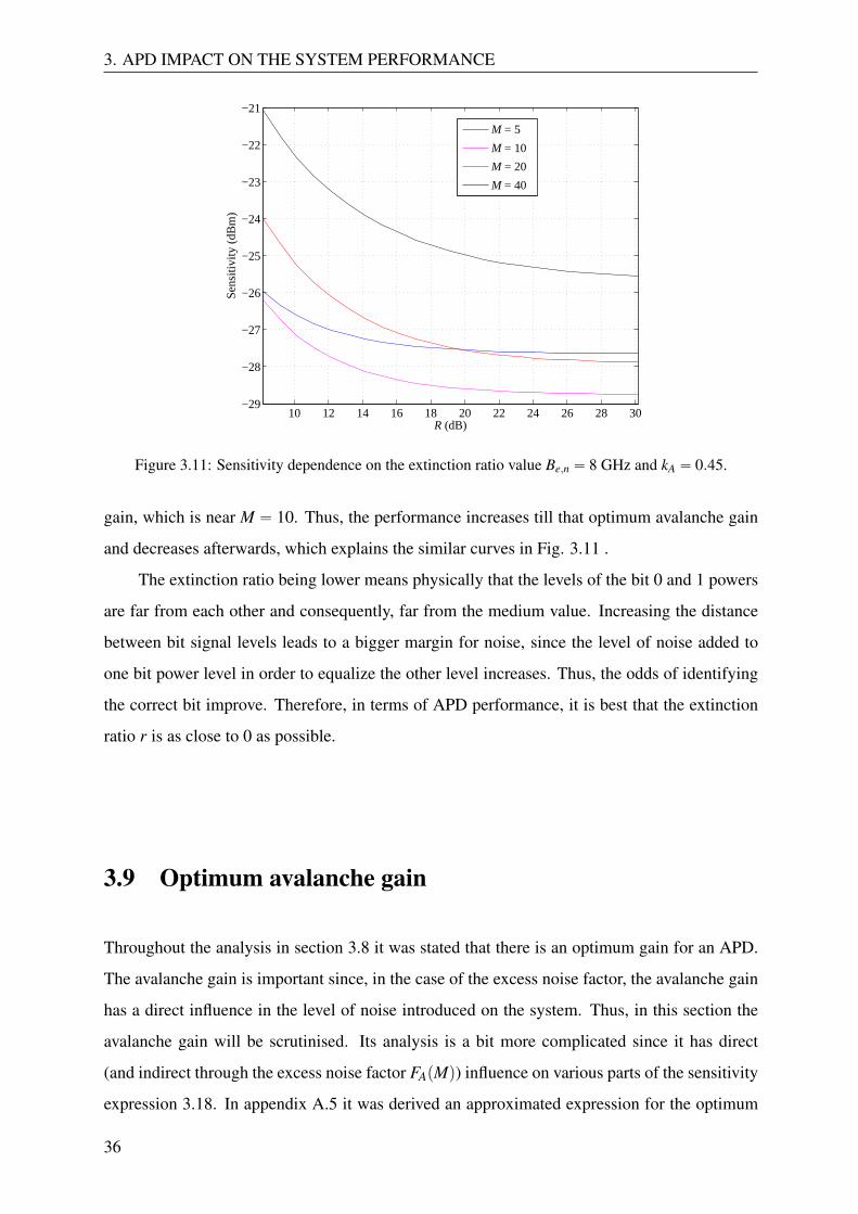
3. APD IMPACT ON THE SYSTEM PERFORMANCE
10 12 14 16 18 20 22 24 26 28 30−29
−28
−27
−26
−25
−24
−23
−22
−21
R (dB)
Sen
sitiv
ity (
dBm
)
M = 5
M = 10
M = 20
M = 40
Figure 3.11: Sensitivity dependence on the extinction ratio value Be,n “ 8 GHz and kA “ 0.45.
gain, which is near M “ 10. Thus, the performance increases till that optimum avalanche gain
and decreases afterwards, which explains the similar curves in Fig. 3.11 .
The extinction ratio being lower means physically that the levels of the bit 0 and 1 powers
are far from each other and consequently, far from the medium value. Increasing the distance
between bit signal levels leads to a bigger margin for noise, since the level of noise added to
one bit power level in order to equalize the other level increases. Thus, the odds of identifying
the correct bit improve. Therefore, in terms of APD performance, it is best that the extinction
ratio r is as close to 0 as possible.
3.9 Optimum avalanche gain
Throughout the analysis in section 3.8 it was stated that there is an optimum gain for an APD.
The avalanche gain is important since, in the case of the excess noise factor, the avalanche gain
has a direct influence in the level of noise introduced on the system. Thus, in this section the
avalanche gain will be scrutinised. Its analysis is a bit more complicated since it has direct
(and indirect through the excess noise factor FApMq) influence on various parts of the sensitivity
expression 3.18. In appendix A.5 it was derived an approximated expression for the optimum
36
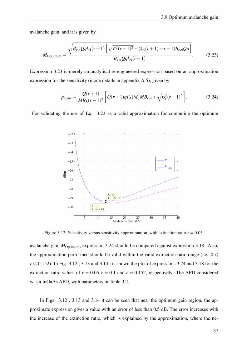
3.9 Optimum avalanche gain
avalanche gain, and it is given by
MOptimum “
c
Be,nQqkApr`1q”
a
σ2cpr´1q2`pkApr`1q´ r´1qBe,nQq
ı
Be,nQqkApr`1q. (3.23)
Expression 3.23 is merely an analytical re-engineered expression based on an approximation
expression for the sensitivity (mode details in appendix A.5), given by
pi,apx “Qpr`1q
MRλpr´1q2
„
Qpr`1qqFApMqMBe,n`
b
σ2cpr´1q2
. (3.24)
For validating the use of Eq. 3.23 as a valid approximation for computing the optimum
5 10 15 20 25 30 35 40
−30
−29
−28
−27
−26
−25
−24
−23
−22
X: 13Y: −29.32
X: 13Y: −29.49
Avalanche Gain (M)
dBm
pipi,apx
Figure 3.12: Sensitivity versus sensitivity approximation, with extinction ratio r “ 0.05.
avalanche gain MOptimum, expression 3.24 should be compared against expression 3.18. Also,
the approximation performed should be valid within the valid extinction ratio range (i.e. 0 ď
r ď 0.152). In Fig. 3.12 , 3.13 and 3.14 , is shown the plot of expressions 3.24 and 3.18 for the
extinction ratio values of r “ 0.05,r “ 0.1 and r “ 0.152, respectively. The APD considered
was a InGaAs APD, with parameters in Table 3.2.
In Figs. 3.12 , 3.13 and 3.14 it can be seen that near the optimum gain region, the ap-
proximate expression gives a value with an error of less than 0.5 dB. The error increases with
the increase of the extinction ratio, which is explained by the approximation, where the ne-
37
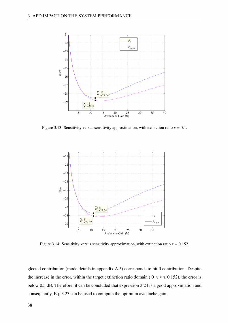
3. APD IMPACT ON THE SYSTEM PERFORMANCE
5 10 15 20 25 30 35 40
−29
−28
−27
−26
−25
−24
−23
−22
−21
X: 12Y: −28.54
X: 12Y: −28.8
Avalanche Gain (M)
dBm
pipi,apx
Figure 3.13: Sensitivity versus sensitivity approximation, with extinction ratio r “ 0.1.
5 10 15 20 25 30 35
−29
−28
−27
−26
−25
−24
−23
−22
−21
X: 11Y: −27.74
X: 11Y: −28.07
Avalanche Gain (M)
dBm
pipi,apx
Figure 3.14: Sensitivity versus sensitivity approximation, with extinction ratio r “ 0.152.
glected contribution (mode details in appendix A.5) corresponds to bit 0 contribution. Despite
the increase in the error, within the target extinction ratio domain ( 0 ď r ď 0.152), the error is
below 0.5 dB. Therefore, it can be concluded that expression 3.24 is a good approximation and
consequently, Eq. 3.23 can be used to compute the optimum avalanche gain.
38
3.10 Conclusion
3.10 Conclusion
In chapter 3, the fundamentals of APD were given. Two points that have impact in the APD
performance: the characterization of the signal and the noise, were described. These points
were discussed using mathematical expressions.
An expression for the sensitivity for an arbitrary extinction ratio was obtained. Thus, it
is possible to compute the sensitivity value given any set of APD parameters, independently
of the input signal characteristics (i.e the extinction ratio value). Furthermore, an analysis of
that expression was presented, leading to a better understanding of how each of its parameters
influence the sensitivity. It was found that the extinction ratio has great impact on the APD per-
formance, and the APD performance is better for lower extinction ratios. Also, it was presented
numerically the improvement of an APD over a normal PIN receiver.
Lastly, an approximated expression for the optimum avalanche gain that leads to the high-
est sensitivity value was achieved. Through that expression the avalanche gain value can be
obtained for any given set of APD parameters, leading to the best sensitivity with an error
below 0.5 dB.
39

3. APD IMPACT ON THE SYSTEM PERFORMANCE
40
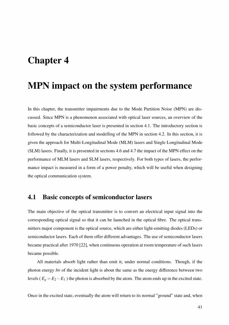
Chapter 4
MPN impact on the system performance
In this chapter, the transmitter impairments due to the Mode Partition Noise (MPN) are dis-
cussed. Since MPN is a phenomenon associated with optical laser sources, an overview of the
basic concepts of a semiconductor laser is presented in section 4.1. The introductory section is
followed by the characterization and modelling of the MPN in section 4.2. In this section, it is
given the approach for Multi-Longitudinal Mode (MLM) lasers and Single Longitudinal Mode
(SLM) lasers. Finally, it is presented in sections 4.6 and 4.7 the impact of the MPN effect on the
performance of MLM lasers and SLM lasers, respectively. For both types of lasers, the perfor-
mance impact is measured in a form of a power penalty, which will be useful when designing
the optical communication system.
4.1 Basic concepts of semiconductor lasers
The main objective of the optical transmitter is to convert an electrical input signal into the
corresponding optical signal so that it can be launched in the optical fibre. The optical trans-
mitters major component is the optical source, which are either light-emitting diodes (LEDs) or
semiconductor lasers. Each of them offer different advantages. The use of semiconductor lasers
became practical after 1970 [22], when continuous operation at room temperature of such lasers
became possible.
All materials absorb light rather than emit it, under normal conditions. Though, if the
photon energy hν of the incident light is about the same as the energy difference between two
levels ( Eg“E2´E1 ) the photon is absorbed by the atom. The atom ends up in the excited state.
Once in the excited state, eventually the atom will return to its normal ”ground” state and, when
41
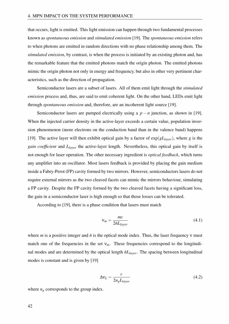
4. MPN IMPACT ON THE SYSTEM PERFORMANCE
that occurs, light is emitted. This light emission can happen through two fundamental processes
known as spontaneous emission and stimulated emission [19]. The spontaneous emission refers
to when photons are emitted in random directions with no phase relationship among them. The
stimulated emission, by contrast, is when the process is initiated by an existing photon and, has
the remarkable feature that the emitted photons match the origin photon. The emitted photons
mimic the origin photon not only in energy and frequency, but also in other very pertinent char-
acteristics, such as the direction of propagation.
Semiconductor lasers are a subset of lasers. All of them emit light through the stimulated
emission process and, thus, are said to emit coherent light. On the other hand, LEDs emit light
through spontaneous emission and, therefore, are an incoherent light source [19].
Semiconductor lasers are pumped electrically using a p´ n junction, as shown in [19].
When the injected carrier density in the active-layer exceeds a certain value, population inver-
sion phenomenon (more electrons on the conduction band than in the valence band) happens
[19]. The active layer will then exhibit optical gain by a factor of exppgLlayerq, where g is the
gain coefficient and Llayer the active-layer length. Nevertheless, this optical gain by itself is
not enough for laser operation. The other necessary ingredient is optical feedback, which turns
any amplifier into an oscillator. Most lasers feedback is provided by placing the gain medium
inside a Fabry-Perot (FP) cavity formed by two mirrors. However, semiconductors lasers do not
require external mirrors as the two cleaved facets can mimic the mirrors behaviour, simulating
a FP cavity. Despite the FP cavity formed by the two cleaved facets having a significant loss,
the gain in a semiconductor laser is high enough so that those losses can be tolerated.
According to [19], there is a phase condition that lasers must match
νm “mc
2nLlayer(4.1)
where m is a positive integer and n is the optical mode index. Thus, the laser frequency ν must
match one of the frequencies in the set νm. These frequencies correspond to the longitudi-
nal modes and are determined by the optical length nLlayer. The spacing between longitudinal
modes is constant and is given by [19]
∆νL “c
2ngLlayer(4.2)
where ng corresponds to the group index.
42
4.2 Characterization of MPN
The gain spectrum is wide enough so that many of the longitudinal modes of the FP cavity
experience gain simultaneously [19]. The mode that is close to the gain peak becomes the dom-
inant mode and the other modes, under ideal conditions, would not reach threshold since their
gain would be less than the main mode. However, due to the extremely small frequency differ-
ence that exists between modes, in practice, some of the neighbouring nodes on each side of the
main mode can carry a significant portion of the laser power. Since each mode propagates in-
side the fibre at slightly different speed due to group-velocity dispersion, the multi-mode nature
of the laser often limits the bit rate of light-wave system. This impairment could be overcome,
improving the performance of the optical system, by designing lasers that oscillate in a single
longitudinal mode, the SLM lasers.
The basic idea for a semiconductor laser that emits light predominantly in a single lon-
gitudinal mode is to design the laser in such a way that the losses are different for different
longitudinal modes of the cavity, as opposing to what happens in FP lasers, whose losses are
independent of the mode. The longitudinal mode that has the smallest cavity loss will achieve
threshold first and, therefore, becomes the dominant mode, while the neighbouring modes have
higher losses. In this case, the power portion carried by these side modes is usually a small
fraction of the total emitted power. For a SLM laser, the side mode suppression is often charac-
terized by the side-mode suppression ratio (SMSR), defined as
SMSR“Pmm
Psm(4.3)
where Pmm is the average power of the main mode and Psm is the average power of the most
dominant side mode. SMSR should be above 30 dB for a good SLM laser [19], which is the
minimum side-mode suppression ratio recommended by ITU-T [20].
4.2 Characterization of MPN
The MPN is related with the laser source. The lasing modes compete at slightly different wave-
lengths leading to fluctuation in the relative portion of the modal powers, though the total output
power remains essentially constant [23]. The optical power fluctuation at different longitudinal-
mode wavelengths interacting with the chromatic dispersion of the fibre results in a random
profile of the output pulse intensity. The random nature of source power distribution among
43
4. MPN IMPACT ON THE SYSTEM PERFORMANCE
longitudinal-mode wavelengths incurs in amplitude and phase noise, simultaneously [23].
Figure 4.1: Random power spectrum at different time instants t1, t2, for illustrating the partitionnoise.
This effect on the optical pulse propagation appears in both single-mode and multi-mode
fibres, as it depends on the interaction between the chromatic dispersion characteristic of the
fibre and the optical source. It can substantially degrade the performance of transmission sys-
tems, operating at high-speeds. In a dispersion-less fibre link, even if the transmission is running
at very high speed, the laser mode partition noise will have no effect. All modes will propa-
gate along the fibre synchronously, avoiding the inter-symbol interference and the consequent
degradation of the signal at the receiver end.
In 1982, Ogawa and Vodhanel stated that the MPN produces an effect of a pulse-delay
fluctuation, and the error rate cannot be reduced by increasing the received signal power [24].
This is an important statement, as it implies that the MPN cannot be mitigated by simply in-
creasing the received signal power. In fact, once the MPN becomes the dominant contribution,
no more improvements can be made in the transmission system [25].
4.3 MPN modeling
In MLM lasers, lasing mode competition causes the mode fluctuations observed during the
injected current transient. Lasing mode competition is the phenomenon in which different res-
onator modes experience laser amplification in the same gain medium. That effect leads to
cross-saturation effects and random occurrences of another phenomenon, known as random
mode partitioning, which is a time-varying laser spectrum.
44
4.3 MPN modeling
For the purposes of the analysis, let us formulate the following assumptions: (a) the total
power carried by each optical pulse emitted by the semiconductor laser is constant; (b) at the end
of the fibre link, the optical waveform detected will be distorted through chromatic dispersion
characteristic of the optical fibre medium; (c) spontaneous emission contribution within each
longitudinal mode is neglected, only stimulated emission is taken into account when assessing
the optical power of each emitted longitudinal mode.
Assuming the laser source emitted N longitudinal modes, and identifying by ci the random
variable representing the relative power of the ith mode, the total relative power is equal to 1, as
given byNÿ
i“1
ci “ 1 (4.4)
where the variable ci is given by the ratio between the power of the ith mode pimode and the total
power ptotal , defined by
ci ”pimode
ptotal. (4.5)
At the end of the fibre link, the total optical pulse shape detected can be expressed by the
sum of each of its partial pulse responses yiptq “ ypt,λiq. Each of them corresponds to each
of the emitted longitudinal modes, being λi the wavelength of the ith mode. Normally, the
chromatic dispersion of the fibre affects every mode differently, so it can be assumed that
ypt,λiq “ ypt,λ jq, i “ j. Therefore, the total pulse response assumes the meaning of a random
process rptq and is given by
rptq “Nÿ
i“1
ypt,λiqci. (4.6)
At the sampling time t “ t0, the measured fluctuation in the detected optical pulse is dependent
on the composition of the N waveforms for every available power distribution. Using expression
4.6, the total detected optical pulse amplitude r0 is also a random variable
r0 ” rpt0q “Nÿ
i“1
ypt0,λiqci ”
Nÿ
i“1
y0pλiqci. (4.7)
The fluctuation of power in the random variable r0 assumes the meaning of mode partition noise
[25]. Using expression 4.7, the variance of MPN is given by[25]
σ2MPN
∆“ xr2
0y´xr0y2. (4.8)
45
4. MPN IMPACT ON THE SYSTEM PERFORMANCE
where xvy stands for the average value of the variable v.
4.3.1 Mode-partition coefficient
To evaluate σMPN , recurring to expression 4.8, expression 4.4 must be examined. The measured
time-average power spectrum Psmpλiq shows the average value of the mode power of each mode
at its λi wavelength
xciy “ Psmpλiq
“
ż
. . .
ż
ciPsmpc1,c2, . . . ,cNq ¨dc1dc2 . . . ,dcN
(4.9)
where Psmpc1,c2, . . . ,cNq is the joint probability distribution function of c1,c2, . . . ,cN . Evaluat-
ing σMPN through expression 4.8 requires that Psmpc1,c2, . . . ,cNq is known, which is generally
not the case. In [27], Ogawa has introduced the concept of mode partition coefficient kMPN
defined by
k2MPN “ 1´α“
xc2i y´xciy
2
xciy´xciy2(4.10)
and it is assumed that xcic jy “ αxciyxc jy for all modes with i “ j where α is a constant. This
assumption translates in practice to assume that every longitudinal mode consists of the stim-
ulated emission, and not spontaneous emission. This assumption is the most critical of this
model, as it may not always be true for semiconductor lasers. However, it allows to evaluate
σMPN without the knowledge of Psmpc1,c2, . . . ,cNq, by using kMPN .
Another form of presentation [25] of kMPN is given by
k2MPN “
Nř
i“1
Nř
j“i`1
`
xciyxc jy´xcic jy˘
Nř
i“1
Nř
j“i`1xciyxc jy
(4.11)
In this form, it can be seen that there are two limiting cases: i) if laser modes are statistically
independent
xcic jy “ xciyxc jy ñ kMPN “ 0 (4.12)
46
4.3 MPN modeling
ii) if laser modes are mutually exclusive
xcic jy “ 0ñ kMPN “ 1. (4.13)
Despite having an expression, the numerical value of kMPN is relatively uncertain and
may depend on a large number of parameters. Nevertheless, a widely used value suggested by
experimental measurements is kMPN “ 0.5 [27].
4.3.2 Mode-partition noise
The variance of MPN, recurring to expressions 4.6 and 4.8, is given by [25]
σ2MPNpkMPNq “ k2
MPN
$
&
%
Nÿ
i“1
y0pλiqxciy´
«
Nÿ
i“1
y0pλiqxciy
ff2,
.
-
(4.14)
It is assumed in expression 4.14 that, after equalization at the receiver, the received signal is of
the form
y0pλiq “ ypλi, t0q “ cosrπBpt0`∆τiqs (4.15)
where B is the bit rate and
∆τi “ LDpλi´λ0q (4.16)
corresponds to the relative delay of the ith partition mode with respect to the central partition
mode λ0, during propagation along a fibre with chromatic dispersion parameter Dλ and length
L. Since the decision circuit samples the signal at times t0 “ N{B, where N is an integer,
expression 4.15 is actually
ypλi, t0q “ cosrπB∆τis. (4.17)
Assuming that xciy can be described by a continuous Gaussian distribution [27], xciy is given
by
xciy “ Psmpλiq “1
σ?
2πexp
„
´pλi´λ0q
2
2σ2
. (4.18)
where σ is the laser r.m.s. spectral width.
Furthermore, considerably simplifying the calculation, the discrete sum in expression 4.14
can be replaced by an integral. Those simplifications allows for calculating the numerical value
47
4. MPN IMPACT ON THE SYSTEM PERFORMANCE
of σMPN . The standard deviation of MPN, σMPN , is then given by
σMPN “kMPN?
2
“
1´ expp´β2q‰
(4.19)
where
β“ πBDλLσ (4.20)
is a dimensionless parameter. The obtained expression 4.19 for the MPN shows that σMPN is
directly proportional to the mode-partition coefficient kMPN defined by expression 4.10.
4.4 MPN in MLM lasers
The MPN effect in MLM lasers can be estimated by adding a noise term to the total noise at
the receiver. This additional noise term is added to the receiver noise so that Q is determined by
[27]1
Q2 “
„ˆ
1` r1´ r
˙
σ0`σ1
2MRλP
2
`
”
σMPN
1
ı2(4.21)
where σ0 and σ1 are the square root of the variances of bits 0 and 1, respectively, P is the average
received signal power at the receiver, r is the extinction ratio, M is the average avalanche gain
of the receiver and Rλ is the responsivity. The power penalty induced by MPN is related to the
received power that is necessary to maintain a constant SNR [26]. Let us consider Qn given by
Qn “
d
Q2
1´Q2σ2MPN
(4.22)
where Q is determined using expression 3.10. Then, expression 4.21 becomes similar to Eq.
A.15 from the appendix A used to derive the sensitivity expresion 3.18. Thus, the power in
the presence of the MPN, Pn, can be obtained by using expression 3.18 using Qn instead of Q.
Morever, the power in absence of MPN, P0, can be obtained using 3.18 using Q. Therefore the
power penalty (in decibels) is given by
αMPN “ 10log10
ˆ
Pn
P0
˙
. (4.23)
The MPN has a critical importance when designing an optical transmission system. For ex-
ample, if the desired BER is 10´12 which corresponds approximately to Q “ 7, the maximum
48
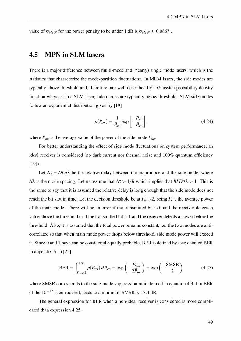
4.5 MPN in SLM lasers
value of σMPN for the power penalty to be under 1 dB is σMPN « 0.0867 .
4.5 MPN in SLM lasers
There is a major difference between multi-mode and (nearly) single mode lasers, which is the
statistics that characterize the mode-partition fluctuations. In MLM lasers, the side modes are
typically above threshold and, therefore, are well described by a Gaussian probability density
function whereas, in a SLM laser, side modes are typically below threshold. SLM side modes
follow an exponential distribution given by [19]
ppPsmq “1
Psmexp
„
´Psm
Psm
, (4.24)
where Psm is the average value of the power of the side mode Psm.
For better understanding the effect of side mode fluctuations on system performance, an
ideal receiver is considered (no dark current nor thermal noise and 100% quantum efficiency
[19]).
Let ∆τ “ DL∆λ be the relative delay between the main mode and the side mode, where
∆λ is the mode spacing. Let us assume that ∆τ ą 1{B which implies that BLD∆λ ą 1. This is
the same to say that it is assumed the relative delay is long enough that the side mode does not
reach the bit slot in time. Let the decision threshold be at Pmm{2, being Pmm the average power
of the main mode. There will be an error if the transmitted bit is 0 and the receiver detects a
value above the threshold or if the transmitted bit is 1 and the receiver detects a power below the
threshold. Also, it is assumed that the total power remains constant, i.e. the two modes are anti-
correlated so that when main mode power drops below threshold, side mode power will exceed
it. Since 0 and 1 have can be considered equally probable, BER is defined by (see detailed BER
in appendix A.1) [25]
BER“ż `8
Pmm{2ppPsmq dPsm “ exp
ˆ
´Pmm
2Psm
˙
“ expˆ
´SMSR
2
˙
(4.25)
where SMSR corresponds to the side-mode suppression ratio defined in equation 4.3. If a BER
of the 10´12 is considered, leads to a minimum SMSR « 17.4 dB.
The general expression for BER when a non-ideal receiver is considered is more compli-
cated than expression 4.25.
49
4. MPN IMPACT ON THE SYSTEM PERFORMANCE
An approach to obtain BER is to consider the side-mode current as a noise current. That ap-
proach is detailed in Appendix B.1. However, it does not account for the fluctuations of the
main mode current.
The main mode current i0,1ptq, for bit 0 or 1, can be considered a random variable with an
associated statistical distribution. If the two mode laser is considered, the total current after the
optical receiver is then given by
iT0,1ptq “ i0,1ptq` isptq (4.26)
where isptq corresponds to the current after the optical receiver resulting from the side-mode.
It is known [31] that the total laser current iT0,1ptq follows a Gaussian distribution. However,
we may define the total current as iT0,1ptq “ IT0,1 ` δiT0,1ptq, where only δiT0,1ptq is a random
variable and corresponds to the fluctuations of the total current. The variable IT0,1 corresponds
to the total average current for bit 0 or 1. Hence, the probability density function for δiT0,1ptq is
given by
pδT0,1pxq “1
σT0,1
?2π
exp
˜
´x2
2σ2T0,1
¸
. (4.27)
Considering the probability of bit 0 and 1 to be equal, the BER is given by
BER“ PpiT0ptq` iG0ptq ą IDqPp0q`PpiT1ptq` iG1ptq ă IDqPp1q. (4.28)
Substituting iT0,1ptq, the BER is given by
BER“12rPpδiT0ptq` iG0ptq ą ID´ IT0 “ ID0q`PpδiT1ptq` iG1ptq ă ID´ IT1 “ ID1qs (4.29)
where iG0,1ptq corresponds to the Gaussian noise current for bits 0 or 1, and ID the decision
threshold. The resulting BER expression (detailed in appendix B.2) is given by
BER“14
»
—
—
–
erfc
¨
˚
˚
˝
ID´ I0´Im
SMSRc
2´
σ2T0`σ2
0
¯
˛
‹
‹
‚
` erfc
¨
˚
˚
˝
I1`Im
SMSR ´ IDc
2´
σ2T1`σ2
1
¯
˛
‹
‹
‚
fi
ffi
ffi
fl
. (4.30)
50
4.5 MPN in SLM lasers
The value of ID that minimizes the BER (details in Appendix B.2) is obtained from:
ID “
b
σ2T1`σ2
1
´
I0`Im
SMSR
¯
`
b
σ2T0`σ2
0
´
I1`Im
SMSR
¯
b
σ2T0`σ2
0`b
σ2T1`σ2
1
(4.31)
Thus, BER is given by
BER“12
erfcˆ
Q?
2
˙
(4.32)
where Q is given by
Q“I1´ I0
b
σ2T0`σ2
0`b
σ2T1`σ2
1
. (4.33)
The variance of bit 0, σ20, and the variance of bit 1, σ2
1, are given by expressions 3.12 and 3.13,
respectively. The variance of the total current after the optical receiver for bit i, σ2Ti
, is given by
(details in Appendix B.2)
σ2Ti“ σ
2mm,i´σ
2sm,i (4.34)
where the variance of the laser intensity noise σ2mmi
is given by
σ2mmi
“ RλMPirl (4.35)
where Pi is the power of bit i and the parameter rl is a measure of the noise level of the incident
optical signal. The parameter rl is considered as the inverse of the SNR of the light emitted by
the transmitter [19]. Typically, the transmitter SNR is better than 20 dB and rl ă 0.01 [19]. The
side-mode noise variance is given by
σ2smi“
ˆ
RλMPi
SMSR
˙2
(4.36)
It has been considered that bit 0 and bit 1 are equally likely to occur. Based on that assumption,
the average current of the main mode Im may be defined as
Im “12
I0`12
I1. (4.37)
51
4. MPN IMPACT ON THE SYSTEM PERFORMANCE
4.6 Penalty for using a MLM laser
When a MLM laser is employed, the power penalty may be calculated using equations 4.19
and 4.23. It was indicated in section 4.3.1 that a common used value for the mode-partition
coefficient is kMPN “ 0.5 [27] and in [29] it is suggested that kMPN is within the 0.6-0.8 range.
So, for the purpose of the analysis, several values of kMPN were considered. In Fig. 4.2, it can
be seen how the penalty is influenced by the dispersion parameter β, for a value of Q “ 7. For
- parameter0 0.1 0.2 0.3 0.4 0.5 0.6 0.7 0.8
Pow
er p
enal
ty (
dB)
0
0.5
1
1.5
2
2.5
3
3.5
4
4.5
5
kMPN
= 1.0
0.8
0.6
0.4
0.2
Figure 4.2: Power penalty when using a MLM laser as a function of β parameter, for various valuesof kMPN for Q“ 7.
a BER level of 10´12 (Q = 7), the power penalty of the MPN in a MLM laser increases greatly
with β. For high values of kMPN , the power penalty may become infinite (i.e. the defined BER
of 10´12 is not achievable) for β values above a certain point. For experimental values of kMPN ,
in the previous specified range of 0.6-0.8, the power penalty becomes infinite for values of β
above 0.5. Therefore, considering the XG-PON bitrate of 10 Gbps and using expression 4.20,
the distance is limited to Lă 1{p10ˆ109πDσq. Considering D“ 17 ps/(nm/km) and σ“ 2nm
[29], the distance is limited to Lă 0.94 km. In Fig. 4.3 ,it is represented the power penalty for a
BER level of 10´3 (Q = 3). It can be seen that, for a higher BER, the mode-partition coefficient
kMPN has less influence on the power penalty.
When designing an optical system, the β parameter is not the used metric. In fact, light-
52
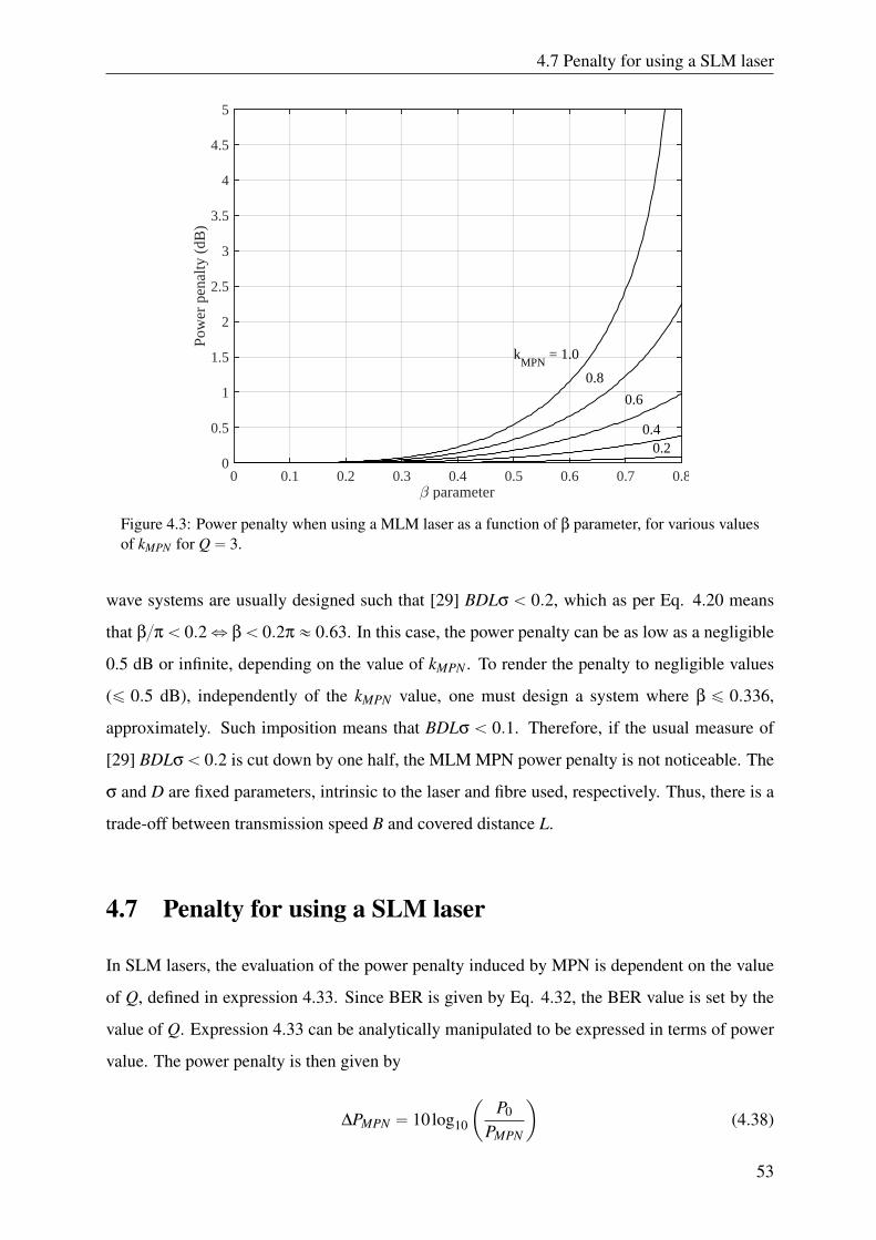
4.7 Penalty for using a SLM laser
- parameter0 0.1 0.2 0.3 0.4 0.5 0.6 0.7 0.8
Pow
er p
enal
ty (
dB)
0
0.5
1
1.5
2
2.5
3
3.5
4
4.5
5
kMPN
= 1.0
0.8
0.6
0.40.2
Figure 4.3: Power penalty when using a MLM laser as a function of β parameter, for various valuesof kMPN for Q“ 3.
wave systems are usually designed such that [29] BDLσ ă 0.2, which as per Eq. 4.20 means
that β{πă 0.2ô βă 0.2π« 0.63. In this case, the power penalty can be as low as a negligible
0.5 dB or infinite, depending on the value of kMPN . To render the penalty to negligible values
(ď 0.5 dB), independently of the kMPN value, one must design a system where β ď 0.336,
approximately. Such imposition means that BDLσ ă 0.1. Therefore, if the usual measure of
[29] BDLσă 0.2 is cut down by one half, the MLM MPN power penalty is not noticeable. The
σ and D are fixed parameters, intrinsic to the laser and fibre used, respectively. Thus, there is a
trade-off between transmission speed B and covered distance L.
4.7 Penalty for using a SLM laser
In SLM lasers, the evaluation of the power penalty induced by MPN is dependent on the value
of Q, defined in expression 4.33. Since BER is given by Eq. 4.32, the BER value is set by the
value of Q. Expression 4.33 can be analytically manipulated to be expressed in terms of power
value. The power penalty is then given by
∆PMPN “ 10log10
ˆ
P0
PMPN
˙
(4.38)
53
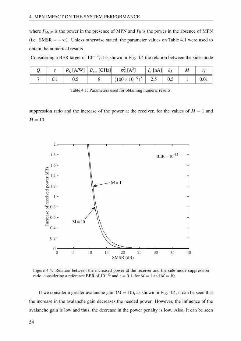
4. MPN IMPACT ON THE SYSTEM PERFORMANCE
where PMPN is the power in the presence of MPN and P0 is the power in the absence of MPN
(i.e. SMSR “ `8). Unless otherwise stated, the parameter values on Table 4.1 were used to
obtain the numerical results.
Considering a BER target of 10´12, it is shown in Fig. 4.4 the relation between the side-mode
Q r Rλ [A/W] Be,n [GHz] σ2c [A2] Id [nA] kA M rl
7 0.1 0.5 8 p100ˆ10´9q2 2.5 0.5 1 0.01
Table 4.1: Parameters used for obtaining numeric results.
suppression ratio and the increase of the power at the receiver, for the values of M “ 1 and
M “ 10.
SMSR (dB)0 5 10 15 20 25 30 35 40
Incr
ease
of r
ecei
ved
pow
er (d
B)
0
0.2
0.4
0.6
0.8
1
1.2
1.4
1.6
1.8
2
M = 10
M = 1
BER = 10-12
Figure 4.4: Relation between the increased power at the receiver and the side-mode suppressionratio, considering a reference BER of 10´12 and r “ 0.1, for M “ 1 and M “ 10.
If we consider a greater avalanche gain (M “ 10), as shown in Fig. 4.4, it can be seen that
the increase in the avalanche gain decreases the needed power. However, the influence of the
avalanche gain is low and thus, the decrease in the power penalty is low. Also, it can be seen
54
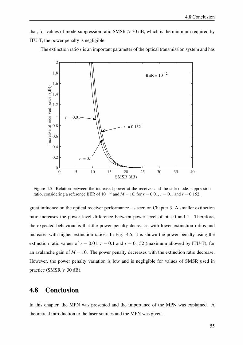
4.8 Conclusion
that, for values of mode-suppression ratio SMSR ě 30 dB, which is the minimum required by
ITU-T, the power penalty is negligible.
The extinction ratio r is an important parameter of the optical transmission system and has
SMSR (dB)0 5 10 15 20 25 30 35 40
Incr
ease
of r
ecei
ved
pow
er (d
B)
0
0.2
0.4
0.6
0.8
1
1.2
1.4
1.6
1.8
2
r = 0.152
r = 0.1
r = 0.01
BER = 10-12
Figure 4.5: Relation between the increased power at the receiver and the side-mode suppressionratio, considering a reference BER of 10´12 and M “ 10, for r “ 0.01, r “ 0.1 and r “ 0.152.
great influence on the optical receiver performance, as seen on Chapter 3. A smaller extinction
ratio increases the power level difference between power level of bits 0 and 1. Therefore,
the expected behaviour is that the power penalty decreases with lower extinction ratios and
increases with higher extinction ratios. In Fig. 4.5, it is shown the power penalty using the
extinction ratio values of r “ 0.01, r “ 0.1 and r “ 0.152 (maximum allowed by ITU-T), for
an avalanche gain of M “ 10. The power penalty decreases with the extinction ratio decrease.
However, the power penalty variation is low and is negligible for values of SMSR used in
practice (SMSR ě 30 dB).
4.8 Conclusion
In this chapter, the MPN was presented and the importance of the MPN was explained. A
theoretical introduction to the laser sources and the MPN was given.
55
4. MPN IMPACT ON THE SYSTEM PERFORMANCE
The MPN due to MLM lasers was discussed. The study of the power penalty study caused
by MPN, when MLM lasers are employed, concluded that, at the XG-PON bitrate of 10 Gbps,
there is a great limitation on the achievable distance.
It was discussed a model for obtaining the BER in presence of MPN with SLM lasers. The
presented model takes into account the fluctuations on the main mode and the noise introduced
by the side mode of the SLM laser. The model is based on the Gaussian approximation for the
total current after the receiver [31] and the model that describes the SLM laser of [32]. However,
the obtained BER expression 4.30 is simpler than BER expression from [32].
The power penalty for SLM lasers, which is obtained using BER expression 4.30, was
discussed. The avalanche gain of the receiver and the extinction ratio have low influence on
the power penalty since the side-mode suppression ratio imposed by ITU-T is SMSR ě 30 dB.
Thus, the effect of MPN is equal for a PIN receiver or an APD receiver. The power penalty is
negligible for values of SMSR above 30 dB.
56
Chapter 5
Assessment of XG-PON reach improvement
In this chapter, it is discussed the improvement of the XG-PON reach when using APDs instead
of a PIN receiver, in the presence of MPN. The assessment is accomplished by considering all
possible combinations of lasers and receivers types at the OLT and ONU.
5.1 Link budget of the XG-PON system
The operation of a XG-PON system requires that the emitted power at the OLT (or ONU)
reaches the ONU (or OLT) at a level that the optical receiver can correctly identify the bits sent,
with a desired BER. As it was seen in Chapter 3, the needed power level at the receiver, Pi,
depends on multiple parameters concerning the type of optical receiver employed as well as
system parameters. A system parameter, defined in the design of the XG-PON system is the
BER. In the following sections, the assessment of XG-PON reach considers a BER target of
10´12, which is the typical case when Forward Error Correction (FEC) is not employed. The
case of FEC employment is also evaluated, which corresponds to a target BER of 10´3. The
receiver sensitivity Pi is also dependent on the employed extinction ratio, which concerns the
optical source. An extinction ratio of r “ 0.1 is considered.
In the XG-PON system, the typical optical budget follows the equation given by [18]
Pr ě Pe´Alink ą Pi (5.1)
where Pr corresponds to the power at the receiver input, Pe is the power emitted at the transmitter
output and Alink is the total attenuation. Typically, it is considered a system margin Ms given by
57
5. ASSESSMENT OF XG-PON REACH IMPROVEMENT
[18]
Ms |dB “ Pe´Alink´ Pi´∆PipDλLq |max (5.2)
where ∆PipDλLq |max is the maximum path penalty due to dispersion in the XG-PON system
transmission, and is set to 2 dB. The system margin Ms should cover a safety margin (due to
unexpected losses) Msa f “ 3 dB and other margins due to ageing and variations in the environ-
ment and temperature. A minimum of Ms “ 6 dB is required for the system margin [18].
The path penalty due to the dispersion is given by
∆PipDλLq |dB“ ∆PipDλLq |LdB `∆PipDλLq |MdB `∆PipDλLq |MPNdB (5.3)
where ∆PipDλLq |MdB is the power penalty associated with the modulated bandwidth, ∆PipDλLq |LdB
is the power penalty associated with the source linewidth and ∆PipDλLq |MPNdB is the power
penalty associated with the MPN.
The attenuation due to the transmission and passive components, Alink, is given by
Alink “ NcAc`NsAs`α f L`NspAsp (5.4)
where Nc is the number of connectors used and Ac is the connector attenuation, Ns is the number
of splices and As is the splices attenuation, Nsp is the number of splitters and Asp is the splitter
attenuation, α is the fibre attenuation per km and L is the distance in km. Thus, the optical
power budget is then given by
Pe ě Pi`Ms`Alink`∆PipDλLq |max (5.5)
By using expressions 5.5 and 5.4, it is obtained the maximum distance L that can be accom-
plished. The maximum distance is given by
LďPe´Pi´Ms´NcAc´NsAs´NspAsp´∆PipDλLq |max
α f. (5.6)
Unless otherwise stated, the parameters used for the XG-PON system are shown in Tables 5.1,
5.2 and 5.3.
Throughout the following section, the APD receiver is compared against a PIN receiver in
order to assess the reach extension when using an APD. Unless otherwise stated, the parameters
58
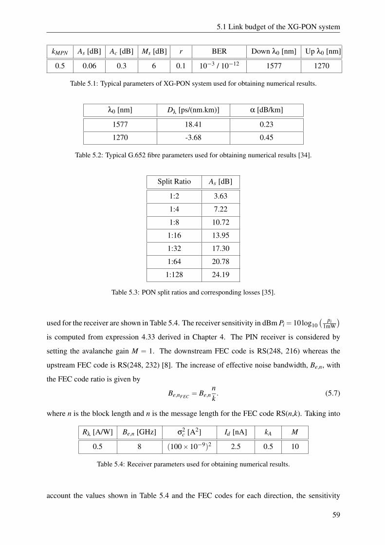
5.1 Link budget of the XG-PON system
kMPN As [dB] Ac [dB] Ms [dB] r BER Down λ0 [nm] Up λ0 [nm]
0.5 0.06 0.3 6 0.1 10´3 / 10´12 1577 1270
Table 5.1: Typical parameters of XG-PON system used for obtaining numerical results.
λ0 [nm] Dλ [ps/(nm.km)] α [dB/km]
1577 18.41 0.23
1270 -3.68 0.45
Table 5.2: Typical G.652 fibre parameters used for obtaining numerical results [34].
Split Ratio As [dB]
1:2 3.63
1:4 7.22
1:8 10.72
1:16 13.95
1:32 17.30
1:64 20.78
1:128 24.19
Table 5.3: PON split ratios and corresponding losses [35].
used for the receiver are shown in Table 5.4. The receiver sensitivity in dBm Pi“ 10log10` pi
1mW
˘
is computed from expression 4.33 derived in Chapter 4. The PIN receiver is considered by
setting the avalanche gain M “ 1. The downstream FEC code is RS(248, 216) whereas the
upstream FEC code is RS(248, 232) [8]. The increase of effective noise bandwidth, Be,n, with
the FEC code ratio is given by
Be,nFEC “ Be,nnk. (5.7)
where n is the block length and n is the message length for the FEC code RS(n,k). Taking into
Rλ [A/W] Be,n [GHz] σ2c [A2] Id [nA] kA M
0.5 8 p100ˆ10´9q2 2.5 0.5 10
Table 5.4: Receiver parameters used for obtaining numerical results.
account the values shown in Table 5.4 and the FEC codes for each direction, the sensitivity
59
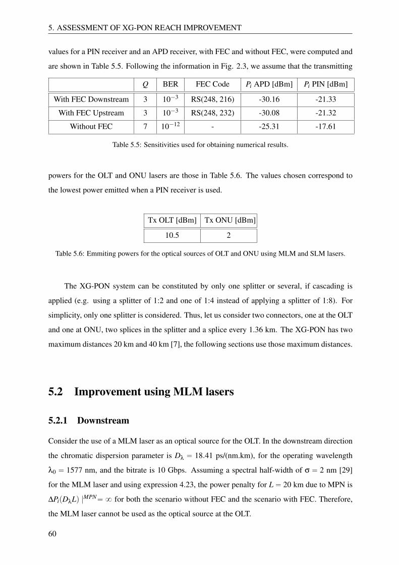
5. ASSESSMENT OF XG-PON REACH IMPROVEMENT
values for a PIN receiver and an APD receiver, with FEC and without FEC, were computed and
are shown in Table 5.5. Following the information in Fig. 2.3, we assume that the transmitting
Q BER FEC Code Pi APD [dBm] Pi PIN [dBm]
With FEC Downstream 3 10´3 RS(248, 216) -30.16 -21.33
With FEC Upstream 3 10´3 RS(248, 232) -30.08 -21.32
Without FEC 7 10´12 - -25.31 -17.61
Table 5.5: Sensitivities used for obtaining numerical results.
powers for the OLT and ONU lasers are those in Table 5.6. The values chosen correspond to
the lowest power emitted when a PIN receiver is used.
Tx OLT [dBm] Tx ONU [dBm]
10.5 2
Table 5.6: Emmiting powers for the optical sources of OLT and ONU using MLM and SLM lasers.
The XG-PON system can be constituted by only one splitter or several, if cascading is
applied (e.g. using a splitter of 1:2 and one of 1:4 instead of applying a splitter of 1:8). For
simplicity, only one splitter is considered. Thus, let us consider two connectors, one at the OLT
and one at ONU, two splices in the splitter and a splice every 1.36 km. The XG-PON has two
maximum distances 20 km and 40 km [7], the following sections use those maximum distances.
5.2 Improvement using MLM lasers
5.2.1 Downstream
Consider the use of a MLM laser as an optical source for the OLT. In the downstream direction
the chromatic dispersion parameter is Dλ “ 18.41 ps/(nm.km), for the operating wavelength
λ0 “ 1577 nm, and the bitrate is 10 Gbps. Assuming a spectral half-width of σ “ 2 nm [29]
for the MLM laser and using expression 4.23, the power penalty for L “ 20 km due to MPN is
∆PipDλLq |MPN“ 8 for both the scenario without FEC and the scenario with FEC. Therefore,
the MLM laser cannot be used as the optical source at the OLT.
60
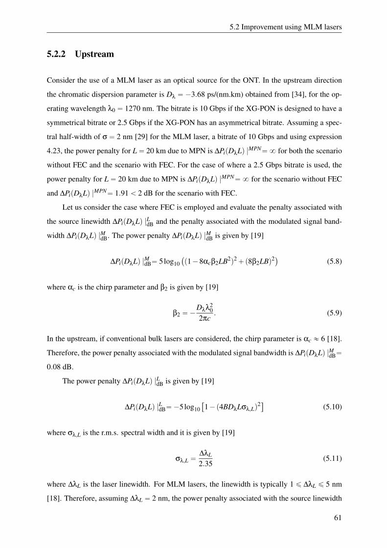
5.2 Improvement using MLM lasers
5.2.2 Upstream
Consider the use of a MLM laser as an optical source for the ONT. In the upstream direction
the chromatic dispersion parameter is Dλ “ ´3.68 ps/(nm.km) obtained from [34], for the op-
erating wavelength λ0 “ 1270 nm. The bitrate is 10 Gbps if the XG-PON is designed to have a
symmetrical bitrate or 2.5 Gbps if the XG-PON has an asymmetrical bitrate. Assuming a spec-
tral half-width of σ “ 2 nm [29] for the MLM laser, a bitrate of 10 Gbps and using expression
4.23, the power penalty for L“ 20 km due to MPN is ∆PipDλLq |MPN“8 for both the scenario
without FEC and the scenario with FEC. For the case of where a 2.5 Gbps bitrate is used, the
power penalty for L “ 20 km due to MPN is ∆PipDλLq |MPN“8 for the scenario without FEC
and ∆PipDλLq |MPN“ 1.91ă 2 dB for the scenario with FEC.
Let us consider the case where FEC is employed and evaluate the penalty associated with
the source linewidth ∆PipDλLq |LdB and the penalty associated with the modulated signal band-
width ∆PipDλLq |MdB. The power penalty ∆PipDλLq |MdB is given by [19]
∆PipDλLq |MdB“ 5log10`
p1´8αcβ2LB2q
2`p8β2LBq2
˘
(5.8)
where αc is the chirp parameter and β2 is given by [19]
β2 “´Dλλ2
02πc
. (5.9)
In the upstream, if conventional bulk lasers are considered, the chirp parameter is αc « 6 [18].
Therefore, the power penalty associated with the modulated signal bandwidth is ∆PipDλLq |MdB“
0.08 dB.
The power penalty ∆PipDλLq |LdB is given by [19]
∆PipDλLq |LdB“´5log10“
1´p4BDλLσλ,Lq2‰ (5.10)
where σλ,L is the r.m.s. spectral width and it is given by [19]
σλ,L “∆λL
2.35(5.11)
where ∆λL is the laser linewidth. For MLM lasers, the linewidth is typically 1 ď ∆λL ď 5 nm
[18]. Therefore, assuming ∆λL “ 2 nm, the power penalty associated with the source linewidth
61
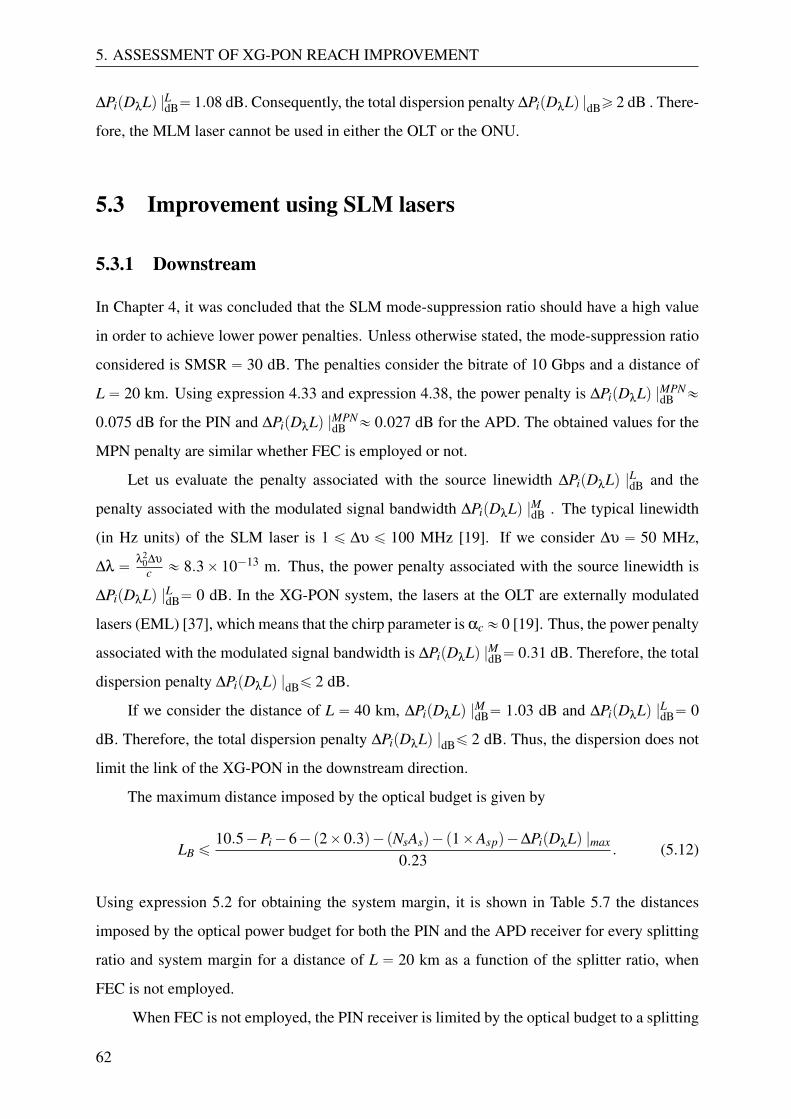
5. ASSESSMENT OF XG-PON REACH IMPROVEMENT
∆PipDλLq |LdB“ 1.08 dB. Consequently, the total dispersion penalty ∆PipDλLq |dBě 2 dB . There-
fore, the MLM laser cannot be used in either the OLT or the ONU.
5.3 Improvement using SLM lasers
5.3.1 Downstream
In Chapter 4, it was concluded that the SLM mode-suppression ratio should have a high value
in order to achieve lower power penalties. Unless otherwise stated, the mode-suppression ratio
considered is SMSR “ 30 dB. The penalties consider the bitrate of 10 Gbps and a distance of
L “ 20 km. Using expression 4.33 and expression 4.38, the power penalty is ∆PipDλLq |MPNdB «
0.075 dB for the PIN and ∆PipDλLq |MPNdB « 0.027 dB for the APD. The obtained values for the
MPN penalty are similar whether FEC is employed or not.
Let us evaluate the penalty associated with the source linewidth ∆PipDλLq |LdB and the
penalty associated with the modulated signal bandwidth ∆PipDλLq |MdB . The typical linewidth
(in Hz units) of the SLM laser is 1 ď ∆υ ď 100 MHz [19]. If we consider ∆υ “ 50 MHz,
∆λ “λ2
0∆υ
c « 8.3ˆ 10´13 m. Thus, the power penalty associated with the source linewidth is
∆PipDλLq |LdB“ 0 dB. In the XG-PON system, the lasers at the OLT are externally modulated
lasers (EML) [37], which means that the chirp parameter is αc« 0 [19]. Thus, the power penalty
associated with the modulated signal bandwidth is ∆PipDλLq |MdB“ 0.31 dB. Therefore, the total
dispersion penalty ∆PipDλLq |dBď 2 dB.
If we consider the distance of L “ 40 km, ∆PipDλLq |MdB“ 1.03 dB and ∆PipDλLq |LdB“ 0
dB. Therefore, the total dispersion penalty ∆PipDλLq |dBď 2 dB. Thus, the dispersion does not
limit the link of the XG-PON in the downstream direction.
The maximum distance imposed by the optical budget is given by
LB ď10.5´Pi´6´p2ˆ0.3q´pNsAsq´p1ˆAspq´∆PipDλLq |max
0.23. (5.12)
Using expression 5.2 for obtaining the system margin, it is shown in Table 5.7 the distances
imposed by the optical power budget for both the PIN and the APD receiver for every splitting
ratio and system margin for a distance of L “ 20 km as a function of the splitter ratio, when
FEC is not employed.
When FEC is not employed, the PIN receiver is limited by the optical budget to a splitting
62
5.3 Improvement using SLM lasers
Splitter ratio PIN max LB [km] APD max LB [km] Ms PIN [dB] Ms APD [dB]
1:2 64.70 98.17 16.28 23.98
1:4 49.09 82.57 12.69 20.39
1:8 33.87 69.00 9.19 16.89
1:16 19.82 54.96 5.96 13.66
1:32 5.26 40.39 2.61 10.31
1:64 -9.87 25.26 -0.87 6.83
1:128 -24.70 10.43 -4.28 3.42
Table 5.7: Maximum distance imposed by the power budget and system margin for L “ 20 km,for both PIN and APD receivers as function of the splitter ratio without FEC, in the downstreamdirection.
ratio of 1:16, whereas the APD receiver supports splitting ratios up to 1:64. The commonly
used splitting ratios are between 1:8 and 1:64 [19]. Thus, the APD covers the use of all com-
mon splitting ratios for L “ 20 km and up to 1:32 for L “ 40 km. In the case where FEC is
employed, the results are in Table 5.8.
The use of a PIN at the ONU allows a splitting ratio up to 1:32, and is limited by the
Splitter ratio PIN max LB [km] APD max LB [km] Ms PIN [dB] Ms APD [dB]
1:2 80.82 118.91 19.99 28.75
1:4 65.21 103.30 16.40 25.16
1:8 50.00 88.43 12.90 21.66
1:16 35.96 74.04 9.67 18.43
1:32 21.39 59.47 6.32 15.08
1:64 6.26 44.35 2.84 11.60
1:128 -8.57 29.52 -0.57 8.19
Table 5.8: Maximum distance imposed by the power budget and system margin for L “ 20 km, forboth PIN and APD receivers as function of the splitter ratio using FEC, in the downstream direction.
optical budget for higher splitting ratios. On the other hand, the APD receiver supports a split-
ting ratio up to 1:128. If we consider a distance of L“ 40 km, the PIN receiver only supports a
splitting ratio up to 1:8 whereas the APD receiver supports up to 1:64 splitting ratio. Again, the
use of an APD covers the use of all common splitting ratios at both L“ 20 km and L“ 40 km.
63
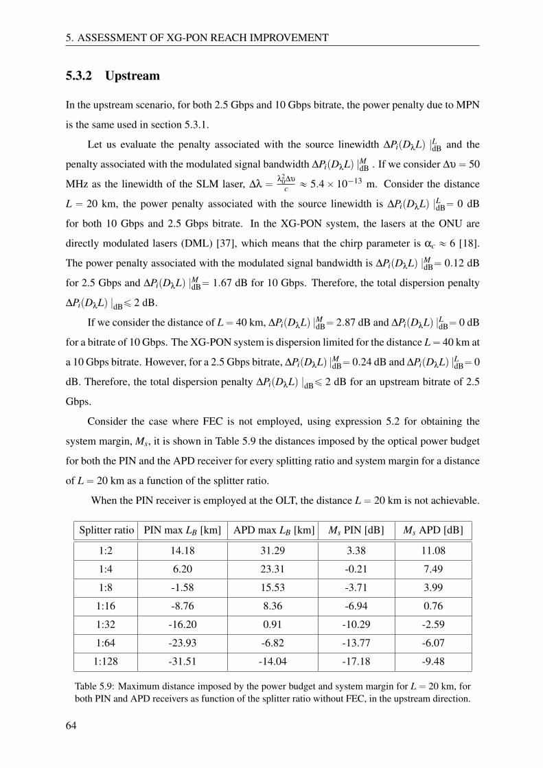
5. ASSESSMENT OF XG-PON REACH IMPROVEMENT
5.3.2 Upstream
In the upstream scenario, for both 2.5 Gbps and 10 Gbps bitrate, the power penalty due to MPN
is the same used in section 5.3.1.
Let us evaluate the penalty associated with the source linewidth ∆PipDλLq |LdB and the
penalty associated with the modulated signal bandwidth ∆PipDλLq |MdB . If we consider ∆υ“ 50
MHz as the linewidth of the SLM laser, ∆λ “λ2
0∆υ
c « 5.4ˆ 10´13 m. Consider the distance
L “ 20 km, the power penalty associated with the source linewidth is ∆PipDλLq |LdB“ 0 dB
for both 10 Gbps and 2.5 Gbps bitrate. In the XG-PON system, the lasers at the ONU are
directly modulated lasers (DML) [37], which means that the chirp parameter is αc « 6 [18].
The power penalty associated with the modulated signal bandwidth is ∆PipDλLq |MdB“ 0.12 dB
for 2.5 Gbps and ∆PipDλLq |MdB“ 1.67 dB for 10 Gbps. Therefore, the total dispersion penalty
∆PipDλLq |dBď 2 dB.
If we consider the distance of L“ 40 km, ∆PipDλLq |MdB“ 2.87 dB and ∆PipDλLq |LdB“ 0 dB
for a bitrate of 10 Gbps. The XG-PON system is dispersion limited for the distance L“ 40 km at
a 10 Gbps bitrate. However, for a 2.5 Gbps bitrate, ∆PipDλLq |MdB“ 0.24 dB and ∆PipDλLq |LdB“ 0
dB. Therefore, the total dispersion penalty ∆PipDλLq |dBď 2 dB for an upstream bitrate of 2.5
Gbps.
Consider the case where FEC is not employed, using expression 5.2 for obtaining the
system margin, Ms, it is shown in Table 5.9 the distances imposed by the optical power budget
for both the PIN and the APD receiver for every splitting ratio and system margin for a distance
of L“ 20 km as a function of the splitter ratio.
When the PIN receiver is employed at the OLT, the distance L“ 20 km is not achievable.
Splitter ratio PIN max LB [km] APD max LB [km] Ms PIN [dB] Ms APD [dB]
1:2 14.18 31.29 3.38 11.08
1:4 6.20 23.31 -0.21 7.49
1:8 -1.58 15.53 -3.71 3.99
1:16 -8.76 8.36 -6.94 0.76
1:32 -16.20 0.91 -10.29 -2.59
1:64 -23.93 -6.82 -13.77 -6.07
1:128 -31.51 -14.04 -17.18 -9.48
Table 5.9: Maximum distance imposed by the power budget and system margin for L “ 20 km, forboth PIN and APD receivers as function of the splitter ratio without FEC, in the upstream direction.
64
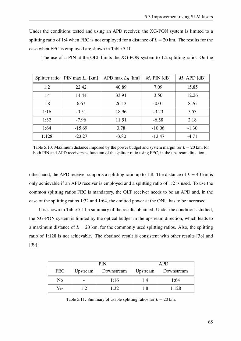
5.3 Improvement using SLM lasers
Under the conditions tested and using an APD receiver, the XG-PON system is limited to a
splitting ratio of 1:4 when FEC is not employed for a distance of L“ 20 km. The results for the
case when FEC is employed are shown in Table 5.10.
The use of a PIN at the OLT limits the XG-PON system to 1:2 splitting ratio. On the
Splitter ratio PIN max LB [km] APD max LB [km] Ms PIN [dB] Ms APD [dB]
1:2 22.42 40.89 7.09 15.85
1:4 14.44 33.91 3.50 12.26
1:8 6.67 26.13 -0.01 8.76
1:16 -0.51 18.96 -3.23 5.53
1:32 -7.96 11.51 -6.58 2.18
1:64 -15.69 3.78 -10.06 -1.30
1:128 -23.27 -3.80 -13.47 -4.71
Table 5.10: Maximum distance imposed by the power budget and system margin for L“ 20 km, forboth PIN and APD receivers as function of the splitter ratio using FEC, in the upstream direction.
other hand, the APD receiver supports a splitting ratio up to 1:8. The distance of L “ 40 km is
only achievable if an APD receiver is employed and a splitting ratio of 1:2 is used. To use the
common splitting ratios FEC is mandatory, the OLT receiver needs to be an APD and, in the
case of the splitting ratios 1:32 and 1:64, the emitted power at the ONU has to be increased.
It is shown in Table 5.11 a summary of the results obtained. Under the conditions studied,
the XG-PON system is limited by the optical budget in the upstream direction, which leads to
a maximum distance of L “ 20 km, for the commonly used splitting ratios. Also, the splitting
ratio of 1:128 is not achievable. The obtained result is consistent with other results [38] and
[39].
PIN APDFEC Upstream Downstream Upstream Downstream
No - 1:16 1:4 1:64
Yes 1:2 1:32 1:8 1:128
Table 5.11: Summary of usable splitting ratios for L“ 20 km.
65
5. ASSESSMENT OF XG-PON REACH IMPROVEMENT
5.4 Conclusion
In this chapter, it was presented an assessment of the XG-PON reach improvement by using an
APD receiver as opposed to a PIN receiver. A set of typical parameters for all XG-PON system
components was presented and the analysis developed was based on those parameters. It was
analysed the use of MLM lasers in downstream and upstream directions. The MLM lasers can-
not be employed due to the high dispersion suffered by the signal emitted by an MLM laser.
Also, it was analysed the use of the SLM lasers in downstream and upstream directions.
In the downstream direction, the use of the APD instead of a PIN at the ONU allows an im-
provement of reach and higher splitting ratio. Furthermore, the use of an APD receiver allows
the use of the common splitting ratios, between 1:8 and 1:64, for distances of L “ 20 km and
L“ 40 km, in the downstream direction. However, under the conditions studied, to achieve the
common splitting ratios in the upstream direction, the use of an APD receiver at the OLT is
mandatory, FEC needs to be employed and the emitting power of the ONU transmitter has to
be increased. Moreover, under the conditions studied, the splitting ratio of 1:128 and a distance
of L“ 40 km was not achieved due to limitations in the upstream direction.
66
Chapter 6
Conclusion and future work
In this chapter, the final conclusions of the work developed in this dissertation are presented, as
well as suggestions for future work.
6.1 Final conclusions
In this dissertation, the assessment of the reach improvement by using APD receivers in the
presence of MPN was performed. Both MLM and SLM laser sources were considered. There-
fore, the optimization of the APD receiver and the model used to characterize the BER in the
presence of MPN gains special relevance in this work. The APD sensitivity was analysed and
an expression for the APD sensitivity for non-null extinction ratio was proposed. In addition, a
model for BER in SLM lasers when MPN is present was proposed and analysed.
In chapter 2, the fundamentals of the XG-PON were given. The possibilities for receivers
and transmitters were reviewed.
In chapter 3, the fundamentals of APD were given, with focus on the factors that influence
the APD performance. An expression for numerically obtain the sensitivity, for an arbitrary ex-
tinction ratio, was derived. Furthermore, an analysis of that expression was presented, leading
to a better understanding of how each of its parameters influence the sensitivity. It was found
that the extinction ratio has great impact on the APD performance, and the APD performance is
better for lower extinction ratios. Also, it was numerically presented how much an APD could
be an improvement over a normal PIN receiver.
An approximated expression for the optimum avalanche gain that leads to the highest sen-
sitivity value was achieved. Through that expression, the avalanche gain value can be obtained
for any given set of APD parameters, leading to the best sensitivity with an error below 0.5 dB.
67
6. CONCLUSION AND FUTURE WORK
In chapter 4, the MPN was presented and the importance of the MPN was explained. A
theoretical introduction to the laser sources and the MPN was given. The MPN due to MLM
lasers was discussed. The study of the power penalty study caused by MPN, when MLM lasers
are employed, concluded that, at the XG-PON bitrate of 10 Gbps, there is a great limitation on
the achievable distance.
It was discussed a model for obtaining the BER in presence of MPN with SLM lasers. The
presented model takes into account the fluctuations on the main mode and the noise introduced
by the side mode of the SLM laser. The model is based on the Gaussian approximation for the
total current at the receiver output [31] and the model that describes the SLM laser of [32]. The
obtained BER expression 4.30 is simpler than BER expression from [32] and is valid for values
of SMSR ě 30 dB.
The power penalty due to MPN for SLM lasers, which is obtained using BER expression
4.30, was discussed. The avalanche gain of the receiver and the extinction ratio have low influ-
ence on the power penalty since the side-mode suppression ratio imposed by ITU-T is SMSR
ě 30 dB. The power penalty is negligible for values of SMSR above 30 dB.
In chapter 5, it was presented an assessment of the improvement of the XG-PON reach by
using an APD receiver as opposed to a PIN receiver. A set of typical parameters for the receiver,
optical fibre and lasers was presented and the analysis developed was based on those parame-
ters. The objective of this assessment was to verify the enhancement of a XG-PON system by
using APD receivers. Additionally, it was intended to study the the MPN effect on the final
solution.
Moreover, it was analysed the use of MLM lasers in both downstream and upstream direc-
tions. The MLM lasers cannot be employed due to the high dispersion suffered by the signal
emitted by an MLM laser.
Furthermore, it was analysed the use of the SLM lasers in the downstream direction and
in the upstream direction. In the downstream direction, the use of an APD instead of a PIN at
the ONU allows an improvement of reach and higher splitting ratio. Furthermore, the use of an
APD receiver allows the use of the common splitting ratios, between 1:8 and 1:64, for distances
of L “ 20 km and L “ 40 km. However, under the conditions studied, to achieve the common
splitting ratios in the upstream direction, the use of an APD receiver at the OLT is mandatory,
FEC needs to be employed and the emitting power of the ONU transmitter has to be increased.
Moreover, under the conditions studied, the splitting ratio of 1:128 was not achieved due to
68
6.2 Future work
limitations in the upstream direction.
6.2 Future work
Following the conclusions drawn above, some work topics for future investigation are suggested
in order to complement or continue the work accomplished in this dissertation:
• Study of the MPN impact in the coexistence of the GPON system and the video overlay
with the XG-PON system,
• Study of the MPN impact in the next-generation PON (NG-PON2).
69

6. CONCLUSION AND FUTURE WORK
70
References
[1] Gigabit-capable passive optical networks (GPON): General characteristics, ITU-T rec-
ommendation G.984.1, 2008.
[2] Gigabit-capable Passive Optical Networks (GPON): Physical Media Dependent (PMD)
layer specification, ITU-T recommendation G.984.2, 2003.
[3] Gigabit-capable Passive Optical Networks (GPON): Transmission convergence layer spec-
ification, ITU-T recommendation G.984.3, 2008.
[4] Gigabit-capable Passive Optical Networks (GPON): ONU management and control inter-
face specification, ITU-T recommendation G.984.4, 2008.
[5] 10-Gigabit-capable passive optical network (XG-PON) systems: Definitions, abbrevia-
tions and acronyms, ITU-T recommendation G.987, 2012.
[6] 10-Gigabit-capable passive optical network (XG-PON) systems: General Requirements,
ITU-T recommendation G.987.1, 2010.
[7] 10-Gigabit-capable passive optical network (XG-PON) systems: Physical media depen-
dent (PMD) layer specification, ITU-T recommendation G.987.2, 2010.
[8] 10-Gigabit-capable passive optical network (XG-PON) systems: Transmission conver-
gence (TC) layer specification, ITU-T recommendation G.987.3, 2010.
[9] S. Pato, P. Monteiro, and H. Silva, “Performance evaluation of the physical layer for
10 Gbit/s Ethernet passive optical networks,” 1st International Conference on Access
Networks, article no. 14, Greece, 2006.
[10] F.J. Effenberger “The XG-PON system: Cost effective 10 Gb/s access,” IEEE/OSA Jour-
nal of Lightwave Technology, vol. 29, no. 4, pp. 403-409, 2011.
[11] Y. Okano, K. Nakagawa, and T. Ito, “Laser mode partition noise evaluation for optical
fiber transmission,” IEEE Transactions on Communications, vol. COM-28, pp. 238-243,
1980.
71
REFERENCES
[12] Q. Zixiong, D. Weichong, Z. Qingke, L. Ning, Z. Qi, L. Changjun, L. Songhau, S. Jian,
C. Xue, C. Lianfeng and Y. Chongxiu, “10 Gb/s transmission over 100 krn of standard
single-mode fiber with a dispersion tunable chirped fiber grating,” SCIENCE IN CHINA,
vol. 42, no. 8, pp. 883-887, 1999.
[13] L. A. Aina, A. Fathimulla and H. Hier, “Ultrasensitive APD photoreceivers for GPON
and longhaul optical transmission,” Optical Fiber Communication Conference, article n
19, United States, 2009.
[14] G. P. Agrawal, “Optical Communication Systems,” Institute of Optics, United States,
2006.
[15] G. Keiser, “Photodetectors,” Optical Fiber Communications, 3rd ed., Singapore: McGraw-
Hill, pp. 243-274, 2009.
[16] Photonics Online, Tutorial : Avalanche Photodiodes Theory And Applications. Available
http://www.photonicsonline.com/doc/avalanche-photodiodes-theory-and-applications-0001
(2005, Dec. 5).
[17] Optical interfaces for equipments and systems relating to the synchronous digital hierar-
chy, ITU-T recommendation G.957, 2006.
[18] A. Cartaxo, “Transmissao por Fibra Optica,” Departamento de Engenharia Electrotecnica
e de Computadores, Instituto Superior Tecnico, 2003.
[19] G. Agrawal, Fiber-Optic Communication Systems, 3rd ed., John Wiley & Sons, Inc.,
2002.
[20] Transmission systems and media, digital systems and networks, ITU-T recommendation
G.959, 2012.
[21] S. Pato, “Analysis and Evaluation of Proposals for Implementation of 10 Gbit/s Ethernet
Passive Optical Networks,” M. Sc. Thesis, Universidade de Coimbra, 2006.
[22] Z. Alferov, “Double heterostructure lasers: early days and the future perspectives,” IEEE
Journal on Selected Topics of Quantum Electronics, vol. 6, No. 6, pp. 832-840, 2000.
[23] K. Pettermann, Laser Diode Modulation and Noise, 1st ed., Springer, 1988.
[24] K. Ogawa, “Analysis of mode partition noise in laser transmission systems,” IEEE Jour-
nal of Quantum Electronics, vol. QE-18, no. 5, pp. 849-855, 1982.
72
REFERENCES
[25] S. Bottacchi, Noise and Signal Interference in Optical Fiber Transmission Systems: An
Optimum Design Approach, 1st ed., John Wiley & Sons, Inc., 2008.
[26] G. Agrawal, P. Anthony, and T. Shen, “Dispersion penalty for 1.3-m lightwave systems
with multimode semiconductor lasers,” IEEE/OSA Journal of Lightwave Technology, vol.
6, no. 5, pp. 620-625, 1988.
[27] W. T. Tsang, Semiconductors and Semimetals. Volume 22: Lightwave Communications
Technology : Part C, Semiconductor Injection Lasers, II Light-Emitting Diodes, 1st ed.,
Academic Press, Inc., 1985.
[28] R. Linke, B. Kasper, C. Burrus, I. Kaminow, J. Ko, and T. Lee, “Mode power partition
events in nearly single-frequency lasers,” IEEE/OSA Journal of Lightwave Technology,
vol. LT-3, no. 3, pp. 706-712, 1985.
[29] M. Mori, Y. Ohkuma, and N. Yamaguchi, “Measurement of mode partition characteristics
of laser diodes modulated by M-sequences,” IEEE/OSA Journal of Lightwave Technology,
vol. 7, no. 7, pp. 1125-1129, 1989.
[30] C. Henry, P. Henry, M. Lax, “Partition fluctuations in nearly single-longitudinal-mode
lasers,” IEEE/OSA Journal of Lightwave Technology, vol. 2, no. 3, pp. 209-216, 1984.
[31] K. Ogawa, P. Liu, “Statistical measurements as a way to study mode partition in injection
lasers,” IEEE/OSA Journal of Lightwave Technology, vol. LT-2, no. 1, pp. 44-48, 1984.
[32] J. Cartledge, “Performance implications of mode partition fluctuations in nearly single
longitudinal mode lasers,” IEEE/OSA Journal of Lightwave Technology, vol. 6, no. 5, pp.
626-635, 1988.
[33] P. A. Bromiley, Products and Convolutions of Gaussian Probability Density Functions,
University of Manchester, 2014.
[34] Prysmian, G.652 Series. Available http://prysmiangroup.com/en/business markets/marke
ts/fibre/products/single-mode/g652-series/ (2015, Jul. 10).
[35] M. Hajduczenia, S. Pato, Channel insertion loss for 1ˆ64 and 1ˆ128 split EPONs,
IEEE802.3 Plenary Meeting, Dallas, 2006.
[36] Thorlabs, Single-Frequency Lasers. Available https://www.thorlabs.com/newgrouppage
9.cfm?objectgroup id=4934 (2015, Jul. 10).
73
REFERENCES
[37] F. Bourgart, “Optical Access Transmission: XG-PON system aspects,” FTTH Confer-
ence, 2010.
[38] L. Frenzel, “What’s the difference between EPON and GPON optical fiber networks?,”
Available http://electronicdesign.com/what-s-difference-between/what-s-difference-betw
een-epon-and-gpon-optical-fiber-networks, (2014, Jan. 6).
[39] Fiberstore, “WDM-PON versus GPON and XG-PON comparison,” Available http://www.
fiberstore.com/wdm-pon-versus-gpon-and-xg-pon-comparison-aid-396.html, (2014, Apr.
29).
[40] J. Kim, H. Bang, C. S. Park, “Design and performance analysis of passively extended
XG-PON with CWDM upstream,” IEEE/OSA Journal of Lightwave Technology, vol. 30,
no. 11, pp. 1677-1684, 2012.
74
Appendix A
APD receiver sensitivity with finite extinc-
tion ratio
In this appendix, it is shown how the expression for the sensitivity of an APD receiver with
non-null extinction ratio is derived. The bit error ratio concept is introduced, leading to the
meaning of the receiver sensitivity. Furthermore, all the necessary steps taken to obtain the
sensitivity expression are described. Still, the obtained general expression for the APD receiver
sensitivity is applied to the case of a PIN receiver, considering unitary gain. Finally, it is derived
an approximated expression for the optimum avalanche gain of an APD receiver.
A.1 Bit error rate
The performance criterion of a digital receiver is the bit-error rate (BER). The BER is custom-
ary defined as the average probability of incorrect bit identification. Ergo, a BER of 1ˆ10´12
corresponds to an average of one error per 1012 bits transmitted. Usually, BER below of 10´9
is the required criterion for a digital receiver. The receiver sensitivity is then defined as the
minimum average power pi required for the receiver to operate with a designed value of BER.
So, in order to compute pi, BER must be calculated.
The sampled value I fluctuates from bit to bit around an average current value I0 or I1,
depending on whether the bit corresponds to 0 or 1 in the bit stream. The decision circuit com-
pares the sampled with a threshold current value ID: calls it bit 1 if I ą ID; calls it bit 0 if I ă ID.
Errors will occur if I ă ID for bit 1 or I ą ID for bit 0, due to receiver noise. Therefore, the BER
can be defined as
BER“ pp1qPp0{1q` pp0qPp1{0q, (A.1)
75
A. APD RECEIVER SENSITIVITY WITH FINITE EXTINCTION RATIO
where pp0q is the probability of receiving bit 0 and Pp1{0q is the probability of deciding 1 when
0 is received. The same for pp1q and Pp0{1q, mutatis mutandis. Assuming the probability of bit
0 equal to bit 1, as they are equally likely to occur, pp0q “ pp1q “ 1{2, BER becomes
BER“12pPp0{1q`Pp1{0qq . (A.2)
The probabilities Pp0{1q and Pp1{0q are very much dependent on the probability density func-
tion ppIq. The functional form of the probability density function ppIq depends on the statistics
of the noise sources responsible for current fluctuations. The shot noise and thermal noise are
well described by Gaussian statistics with zero mean and variances σ2s and σ2
c , respectively.
Note that this is true for PIN receivers. In the case of APD receivers, the shot noise being
treated as a Gaussian random variable is a common approximation, with a different expression
for the variance σ2s [19]. Since, statistically, the sum of two Gaussian random variables is itself
a Gaussian random variable, the variance of the probability density function of I is the sum of
the variances of the noises. Still, variances and average are different for each of the bits, so the
variances to take into account are σ20 and σ2
1. With that in mind, the conditional probabilities
are expressed by [19]
Pp0{1q “1
σ1?
2π
ż ID
´8
expˆ
´pI´ I1q
2
2σ21
˙
dI “12
erfcˆ
I1´ ID
σ1?
2
˙
, (A.3)
Pp1{0q “1
σ0?
2π
ż 8
ID
expˆ
´pI´ I0q
2
2σ20
˙
dI “12
erfcˆ
ID´ I0
σ0?
2
˙
, (A.4)
where erfc is the commonly used complementary error function [19] given by
erfcpxq “2?
π
ż 8
xexpp´y2
qdy. (A.5)
Replacing expressions A.3 and A.4 in the BER expression A.2 results in
BER“14
„
erfcˆ
I1´ ID
σ1?
2
˙
` erfcˆ
ID´ I0
σ0?
2
˙
. (A.6)
The expression A.6 shows the BER dependency of ID. In fact, in practice ID is optimized to
minimize BER, thus the minimum occurs when ID is chosen to verify
pID´ I0q2
2σ20
“pI1´ IDq
2
2σ21
` lnˆ
σ1
σ0
˙
. (A.7)
76
A.2 Preparatory steps
For most relevant cases, the last term may be neglected, which results in
pID´ I0q
σ0“pI1´ IDq
σ1” Q. (A.8)
For most PIN receivers, the decision threshold ID is placed in the middle ID “ pI0` I1q{2,σ1 “
σ0, since the noise domination factor is the thermal noise (σc " σs) and is independent of the
average current. For APD receivers, to set the decision threshold in order to minimize BER, the
explicit ID expression can be used
ID “σ0I1`σ1I0
σ0`σ1. (A.9)
Using expressions A.6 and B.27, the BER expression, only depending on the quality parameter
Q is given by
BER“12
erfcˆ
Q?
2
˙
«expp´Q2{2q
Q?
2π(A.10)
with Q parameter being obtained by expressions B.27 and A.9. The Q parameter is then given
by
Q“I1´ I0
σ1`σ0. (A.11)
For BER it was made an approximation by using the asymptotic expansion [19] of erfcpQ{?
2q
which is reasonably accurate for Q ą 3. Thus, since wanted values of BER are lower than
10´9 (which corresponds roughly to Q “ 5) and Q increases with the decrease of BER, the
approximation is valid.
A.2 Preparatory steps
The extinction ratio r is defined as quotient of the power when the light source is off (bit 0),
commonly defined as pi,0, and the power when the light source is on (bit 1), known as pi,1
r “pi,0
pi,1. (A.12)
It could, also, be defined as the inverse fraction rext “ pi,1{pi,0, though in that case it is com-
monly represented in dB, R “ 10logprextq “ 10logp1{rq. Once r is defined, it is possible to
77
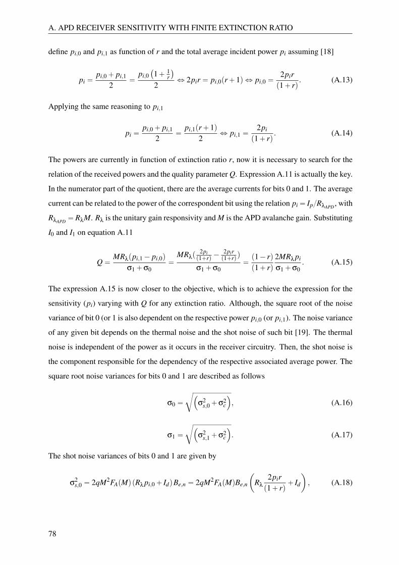
A. APD RECEIVER SENSITIVITY WITH FINITE EXTINCTION RATIO
define pi,0 and pi,1 as function of r and the total average incident power pi assuming [18]
pi “pi,0` pi,1
2“
pi,0`
1` 1r
˘
2ô 2pir “ pi,0pr`1q ô pi,0 “
2pirp1` rq
. (A.13)
Applying the same reasoning to pi,1
pi “pi,0` pi,1
2“
pi,1pr`1q2
ô pi,1 “2pi
p1` rq. (A.14)
The powers are currently in function of extinction ratio r, now it is necessary to search for the
relation of the received powers and the quality parameter Q. Expression A.11 is actually the key.
In the numerator part of the quotient, there are the average currents for bits 0 and 1. The average
current can be related to the power of the correspondent bit using the relation pi“ Ip{RλAPD , with
RλAPD “RλM. Rλ is the unitary gain responsivity and M is the APD avalanche gain. Substituting
I0 and I1 on equation A.11
Q“MRλppi,1´ pi,0q
σ1`σ0“
MRλp2pip1`rq ´
2pirp1`rqq
σ1`σ0“p1´ rqp1` rq
2MRλ pi
σ1`σ0. (A.15)
The expression A.15 is now closer to the objective, which is to achieve the expression for the
sensitivity (pi) varying with Q for any extinction ratio. Although, the square root of the noise
variance of bit 0 (or 1 is also dependent on the respective power pi,0 (or pi,1). The noise variance
of any given bit depends on the thermal noise and the shot noise of such bit [19]. The thermal
noise is independent of the power as it occurs in the receiver circuitry. Then, the shot noise is
the component responsible for the dependency of the respective associated average power. The
square root noise variances for bits 0 and 1 are described as follows
σ0 “
c
´
σ2s,0`σ2
c
¯
, (A.16)
σ1 “
c
´
σ2s,1`σ2
c
¯
. (A.17)
The shot noise variances of bits 0 and 1 are given by
σ2s,0 “ 2qM2FApMqpRλ pi,0` IdqBe,n “ 2qM2FApMqBe,n
ˆ
Rλ
2pirp1` rq
` Id
˙
, (A.18)
78
A.3 Deriving APD sensitivity expression
σ2s,1 “ 2qM2FApMqpRλ pi,1` IdqBe,n “ 2qM2FApMqBe,n
ˆ
Rλ
2pi
p1` rq` Id
˙
. (A.19)
As mentioned, the thermal noise is not dependent on the power so, it is independent of the
receiver being a PIN or an APD. Also, from the computation perspective, it would introduce
more parameters to take into account, so there is no need to replace σ2c for its expression.
The shot noise expression introduces another level of dependency, as the shot noise on
APD is also affected by another term: the excess noise factor FApMq [19] given by
FApMq “ kAM`p1´ kAqp2´1{Mq. (A.20)
Nevertheless, there is no need for substituting this additional noise factor for its expression A.20
in the shot noise expression as it will complicate even more the steps towards the result and,
ultimately, it could not simplify the result. So, it will be treated as another variable. With all
variables in (A.11) scrutinized, starting to derive the expression in order to pi is the next step.
A.3 Deriving APD sensitivity expression
The natural course of action would be to replace σ1 and σ0 in expression A.15 and compute the
result from there. That will make A.15 a very big expression. Ergo, some auxiliary variables
will be created instead, aggregating some of the variables that repeat, (such as the responsivity
or the effective noise bandwidth). That way the expression is more simple to be comprehended
and more readable. Let n be
n“ 2MRλ
p1´ rqp1` rq
(A.21)
and u be
u“ 2qM2FApMqBe,n. (A.22)
These help variables just created, are then applied in the shot noise variance expression, result-
ing in
Q“npi
c
´´
Rλ2pip1`rq ` Id
¯
u`σ2c
¯
`
c
´´
Rλ2pirp1`rq ` Id
¯
u`σ2c
¯
. (A.23)
Solving this expression by hand is very laborious due to its number of variables (even if the
auxiliary variables created are not replaced by their corresponding expression). Hence, the
whole expression was introduced into MATLAB, replacing the auxiliary variables for their val-
79
A. APD RECEIVER SENSITIVITY WITH FINITE EXTINCTION RATIO
ues, leading to the complete full expression. Such expression was then passed as an argument
to the MATLAB function solve, which solved the expression in order to pi variable, as wished.
Two solutions were obtained, solution one
pi “Qpr`1q
MRλpr´1q2
„
QqFApMqMBe,npr`1q
`
b
p2qFApMqM2Be,nId`σ2cqpr´1q2` rp2QqFApMqMBe,nq2
(A.24)
and solution two
pi “Qpr`1q
MRλpr´1q2
„
QqFApMqMBe,npr`1q
´
b
p2qFApMqM2Be,nId`σ2cqpr´1q2` rp2QqFApMqMBe,nq2
. (A.25)
The aimed solution has to have certain characteristics thus, some limitations must be imposed.
Therefore, to determine which of the solutions is the correct one, a simple imposition is made.
Since pi corresponds to a power value, physically only positive values have meaning. Thus, the
chosen solution must be always positive, in the operation domain (M ą 0).
A simple procedure for analysing both solutions consists in plotting the two functions, using
Q r Rλ [A/W] Be,n [GHz] σ2c [A2] Id [nA] kA
7 0.152 0.73 8 p100ˆ10´9q2 100 0.9
Table A.1: Set of typical values for sensitivity parameters for testing the two sensitivity solutions.
typical parameters Table A.1 and making M varying in the wanted domain. It is possible to
see, after examination of the procedure result shown in Fig. A.1, that solution two has negative
values for the sensitivity. That violates the simple imposition made, as it is not physically
possible. Ergo, solution two is excluded, leaving solution one expression A.24, as the correct
solution.
80
A.4 APD sensitivity applied to PIN
5 10 15 20 25 30−150
−100
−50
0
50
100
150
Avalanche Gain (M)
Sen
sitiv
ity (µ
W)
Solution 1Solution 2
Figure A.1: Sensitivity values for both solutions presented.
A.4 APD sensitivity applied to PIN
The sensitivity obtained expression A.24 is also valid for a PIN diode receiver, (considering
a PIN as a unitary gain APD M “ 1). The value of FApMq in that case is 1, as displayed by
expression A.26.
FApMq “ kA`p1´ kAqp2´1q “ kA´ kA`1“ 1. (A.26)
Hence, the final expression for a PIN is given by
pi “Qpr`1q
MRλpr´1q2
„
QqFApMqMBe,npr`1q
`
b
p2qFApMqM2Be,nId`σ2cqpr´1q2` rp2QqFApMqMBe,nq2
“Qpr`1q
Rλpr´1q2
„
QqBe,npr`1q`b
p2qBe,nId`σ2cqpr´1q2` rp2QqBe,nq2
(A.27)
A.5 Deriving the APD optimum gain
By inspecting Fig. A.1, due to the evolving pattern of the sensitivity curve (solution 1), there is
indication that only one value of M optimizes the sensitivity. When that gain value is reached,
the maximum sensitivity is achieved. As so, theoretically the optimum gain can be obtained
by following a series of steps: differentiating the expression A.24 in order to M; After the
differentiation is complete, the differentiated expression is equalized to zero; Then, the result
expression is solved in order to the avalanche gain M, obtaining the expression for the optimum
81
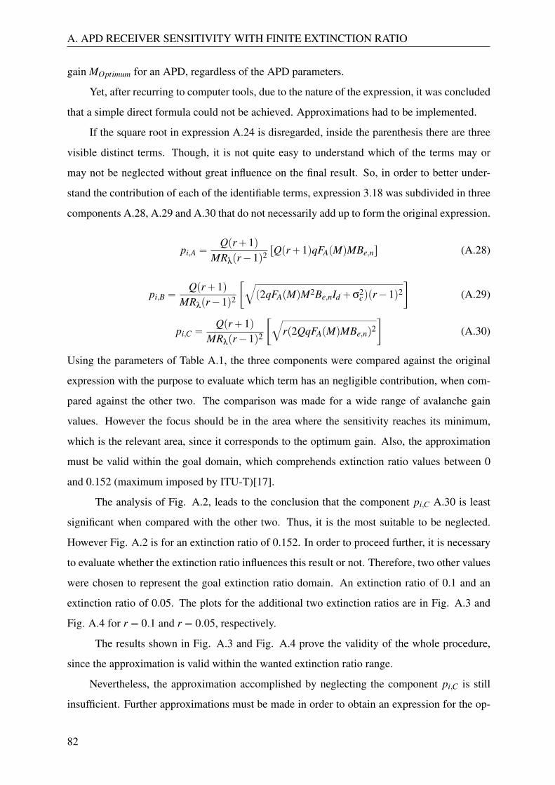
A. APD RECEIVER SENSITIVITY WITH FINITE EXTINCTION RATIO
gain MOptimum for an APD, regardless of the APD parameters.
Yet, after recurring to computer tools, due to the nature of the expression, it was concluded
that a simple direct formula could not be achieved. Approximations had to be implemented.
If the square root in expression A.24 is disregarded, inside the parenthesis there are three
visible distinct terms. Though, it is not quite easy to understand which of the terms may or
may not be neglected without great influence on the final result. So, in order to better under-
stand the contribution of each of the identifiable terms, expression 3.18 was subdivided in three
components A.28, A.29 and A.30 that do not necessarily add up to form the original expression.
pi,A “Qpr`1q
MRλpr´1q2rQpr`1qqFApMqMBe,ns (A.28)
pi,B “Qpr`1q
MRλpr´1q2
„
b
p2qFApMqM2Be,nId`σ2cqpr´1q2
(A.29)
pi,C “Qpr`1q
MRλpr´1q2
„
b
rp2QqFApMqMBe,nq2
(A.30)
Using the parameters of Table A.1, the three components were compared against the original
expression with the purpose to evaluate which term has an negligible contribution, when com-
pared against the other two. The comparison was made for a wide range of avalanche gain
values. However the focus should be in the area where the sensitivity reaches its minimum,
which is the relevant area, since it corresponds to the optimum gain. Also, the approximation
must be valid within the goal domain, which comprehends extinction ratio values between 0
and 0.152 (maximum imposed by ITU-T)[17].
The analysis of Fig. A.2, leads to the conclusion that the component pi,C A.30 is least
significant when compared with the other two. Thus, it is the most suitable to be neglected.
However Fig. A.2 is for an extinction ratio of 0.152. In order to proceed further, it is necessary
to evaluate whether the extinction ratio influences this result or not. Therefore, two other values
were chosen to represent the goal extinction ratio domain. An extinction ratio of 0.1 and an
extinction ratio of 0.05. The plots for the additional two extinction ratios are in Fig. A.3 and
Fig. A.4 for r “ 0.1 and r “ 0.05, respectively.
The results shown in Fig. A.3 and Fig. A.4 prove the validity of the whole procedure,
since the approximation is valid within the wanted extinction ratio range.
Nevertheless, the approximation accomplished by neglecting the component pi,C is still
insufficient. Further approximations must be made in order to obtain an expression for the op-
82
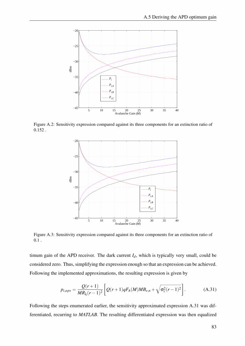
A.5 Deriving the APD optimum gain
5 10 15 20 25 30 35 40−45
−40
−35
−30
−25
−20
Avalanche Gain (M)
dBm
pi
pi,A
pi,B
pi,C
Figure A.2: Sensitivity expression compared against its three components for an extinction ratio of0.152 .
5 10 15 20 25 30 35 40−45
−40
−35
−30
−25
−20
Avalanche Gain (M)
dBm
pi
pi,A
pi,B
pi,C
Figure A.3: Sensitivity expression compared against its three components for an extinction ratio of0.1 .
timum gain of the APD receiver. The dark current Id , which is typically very small, could be
considered zero. Thus, simplifying the expression enough so that an expression can be achieved.
Following the implemented approximations, the resulting expression is given by
pi,apx “Qpr`1q
MRλpr´1q2
„
Qpr`1qqFApMqMBe,n`
b
σ2cpr´1q2
. (A.31)
Following the steps enumerated earlier, the sensitivity approximated expression A.31 was dif-
ferentiated, recurring to MATLAB. The resulting differentiated expression was then equalized
83
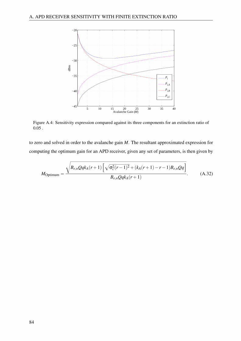
A. APD RECEIVER SENSITIVITY WITH FINITE EXTINCTION RATIO
5 10 15 20 25 30 35 40−45
−40
−35
−30
−25
−20
Avalanche Gain (M)
dBm
pi
pi,A
pi,B
pi,C
Figure A.4: Sensitivity expression compared against its three components for an extinction ratio of0.05 .
to zero and solved in order to the avalanche gain M. The resultant approximated expression for
computing the optimum gain for an APD receiver, given any set of parameters, is then given by
MOptimum “
c
Be,nQqkApr`1q”
a
σ2cpr´1q2`pkApr`1q´ r´1qBe,nQq
ı
Be,nQqkApr`1q. (A.32)
84
Appendix B
Auxiliary derivations related to MPN
B.1 BER in SLM lasers
Due to the nature of the nearly single-mode lasers behaviour, its partition mode fluctuations
cannot be treated as a Gaussian random variable. Actually, it has been observed that its proba-
bility density function exhibits a exponential distribution behaviour [28]. In order to calculate
the BER, it is necessary to add the contribution of the shot and thermal noises, whose proba-
bility density functions are well approximated by Gaussian distributions, and the contribution
from the MPN noise, which, as stated, follows an exponential distribution.
Considering the total noise current to be inptq, the Gaussian noise current to be iGptq and the
exponential noise current be iexpptq
inptq “ iGptq` iexpptq. (B.1)
Let us consider that bits 0 and 1 are two different random variables iG0ptq and iG1ptq, respec-
tively. Thus, iG0ptq and iG1ptq have different standard deviations and, therefore, different proba-
bility distributions . The corresponding probability density functions of iG0ptq, iG1ptq and iexpptq
are, respectively
pG0pxq “1
σ0?
2πexp
ˆ
´x2
2σ20
˙
. (B.2)
pG1pxq “1
σ1?
2πexp
ˆ
´x2
2σ21
˙
. (B.3)
pexppyq “
$
’
&
’
%
1b
exp´
´yb
¯
, yě 0
0, yă 0(B.4)
85
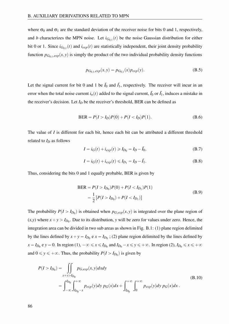
B. AUXILIARY DERIVATIONS RELATED TO MPN
where σ0 and σ1 are the standard deviation of the receiver noise for bits 0 and 1, respectively,
and b characterizes the MPN noise. Let iG0,1ptq be the noise Gaussian distribution for either
bit 0 or 1. Since iG0,1ptq and iexpptq are statistically independent, their joint density probability
function pG0,1,exppx,yq is simply the product of the two individual probability density functions
pG0,1,exppx,yq “ pG0,1pxqpexppyq. (B.5)
Let the signal current for bit 0 and 1 be I0 and I1, respectively. The receiver will incur in an
error when the total noise current inptq added to the signal current, I0 or I1, induces a mistake in
the receiver’s decision. Let ID be the receiver’s threshold, BER can be defined as
BER“ PpI ą IDqPp0q`PpI ă IDqPp1q. (B.6)
The value of I is different for each bit, hence each bit can be attributed a different threshold
related to ID as follows
I “ iGptq` iexpptq ě ID0 “ ID´ I0, (B.7)
I “ iGptq` iexpptq ď ID1 “ ID´ I1. (B.8)
Thus, considering the bits 0 and 1 equally probable, BER is given by
BER“ PpI ą ID0qPp0q`PpI ă ID1qPp1q
“12rPpI ą ID0q`PpI ă ID1qs
(B.9)
The probability PpI ą ID0q is obtained when pG,exppx,yq is integrated over the plane region of
(x,y) where x` yą ID0 . Due to its distribution, y will be zero for values under zero. Hence, the
integration area can be divided in two sub areas as shown in Fig. B.1: (1) plane region delimited
by the lines defined by x` y“ ID0 e x“ ID0 ; (2) plane region delimited by the lines defined by
x“ ID0 e y“ 0. In region (1),´8ď xď ID0 and ID0´xď yď`8. In region (2), ID0 ď xď`8
and 0ď yď`8. Thus, the probability PpI ą ID0q is given by
PpI ą ID0q “
ij
x`yąID0
pG,exppx,yqdxdy
“
ż ID0
´8
ż `8
ID0´xpexppyqdy pGpxqdx`
ż `8
ID0
ż `8
0pexppyqdy pGpxqdx .
(B.10)
86
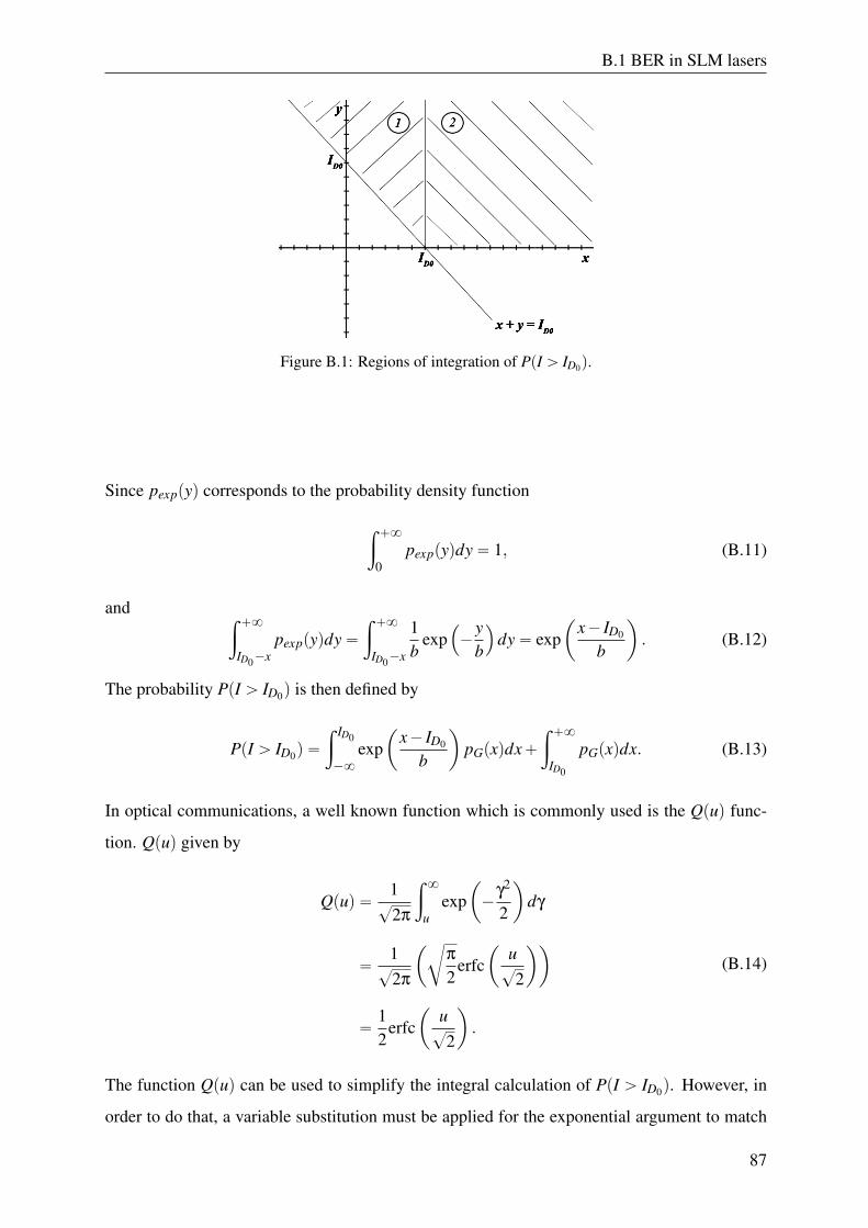
B.1 BER in SLM lasers
ID0
ID0
x
y
x + y = ID0
Figure B.1: Regions of integration of PpI ą ID0q.
Since pexppyq corresponds to the probability density function
ż `8
0pexppyqdy“ 1, (B.11)
andż `8
ID0´xpexppyqdy“
ż `8
ID0´x
1b
exp´
´yb
¯
dy“ expˆ
x´ ID0
b
˙
. (B.12)
The probability PpI ą ID0q is then defined by
PpI ą ID0q “
ż ID0
´8
expˆ
x´ ID0
b
˙
pGpxqdx`ż `8
ID0
pGpxqdx. (B.13)
In optical communications, a well known function which is commonly used is the Qpuq func-
tion. Qpuq given by
Qpuq “1?
2π
ż 8
uexp
ˆ
´γ2
2
˙
dγ
“1?
2π
ˆ
c
π
2erfc
ˆ
u?
2
˙˙
“12
erfcˆ
u?
2
˙
.
(B.14)
The function Qpuq can be used to simplify the integral calculation of PpI ą ID0q. However, in
order to do that, a variable substitution must be applied for the exponential argument to match
87
B. AUXILIARY DERIVATIONS RELATED TO MPN
´γ
2 . In the case of PpI ą ID0q, a substitution can be made by defining γ as
γ“xσ´
σ
b, (B.15)
using
dγ“1σ
dx. (B.16)
Applying the variable substitution to B.13
PpI ą ID0q “
ż ID0
´8
expˆ
x´ ID0
b
˙
pGpxqdx`ż `8
ID0
pGpxqdx.
“
exp´
´ID0b
¯
?2π
ż ID0
´8
1σ0
expˆ
´x2
2σ20`
xb´
σ20
2b2 `σ2
02b2
˙
dx`1?
2π
ż `8
ID0
1σ0
expˆ
´x2
2σ20
˙
dx
“
exp´
´ID0b `
σ20
2b2
¯
?2π
ż
ID0σ0´
σ0b
´8
expˆ
´γ2
2
˙
dγ`1?
2π
ż `8
ID0{σ0
expˆ
´γ2
2
˙
dγ
“ expˆ
´ID0
b`
σ20
2b2
˙„
1´Qˆ
ID0
σ0´
σ0
b
˙
`Qˆ
ID0
σ0
˙
.
(B.17)
On the other hand, the probability PpI ă ID1q implies that x` y ď ID1 . As before, y is zero for
ID0
ID0
x
y
x + y = ID0
Figure B.2: Region of integration of PpI ă ID1q.
values under zero. The integration area is defined by the region plane contained by the lines
defined by x`y“ ID1 and y“ 0, as shown in Fig. B.2 . With 0ď yď ID1´x and´8ď xď ID1 .
88
B.1 BER in SLM lasers
PpI ă ID1q is given by
PpI ă ID1q “
ij
x`yăID1
pG,exppx,yqdxdy
“
ż ID1
´8
ż ID1´x
0pexppyqdy pGpxqdx
“
ż ID1
´8
„
1´ expˆ
x´ ID1
b
˙
pGpxqdx.
(B.18)
In order to use Qpuq to simplify the integral calculation of PpI ă ID1q, a variable substitution
must be applied for the exponential argument to match´ γ
2 . In the case of PpI ă ID1q the variable
substitution can be accomplished by defining γ as
γ“xσ, (B.19)
using
dγ“1σ
dx. (B.20)
Applying the variable substitution to B.18
PpI ă ID1q “
ż ID1
´8
„
1´ expˆ
x´ ID1
b
˙
pGpxqdx
“
ż ID1
´8
pGpxqdx´ż ID1
´8
expˆ
x´ ID1
b
˙
pGpxqdx
“ 1´Qˆ
ID1
σ1
˙
´ expˆ
´ID1
b`
σ21
2b2
˙„
1´Qˆ
ID1
σ1´
σ1
b
˙
.
. (B.21)
The BER is then given by
BER“12
„
expˆ
´ID0
b`
σ20
2b2
˙„
1´Qˆ
ID0
σ0´
σ0
b
˙
`Qˆ
ID0
σ0
˙
` 1´Qˆ
ID1
σ1
˙
´ expˆ
´ID1
b`
σ21
2b2
˙„
1´Qˆ
ID1
σ1´
σ1
b
˙
.
(B.22)
Previously, the b value of expression B.4 was left undefined. The value of b characterizes the
MPN noise, so it is necessary to define it. The nature of a single-mode laser is quantified by the
mode suppression ration (SMSR), which is defined as the ratio of the main mode power Pmm
and the most dominant side mode power Psm. The MPN noise in a nearly single-mode laser
is related to the fluctuations of the power of the side mode. The side mode power follows a
89
B. AUXILIARY DERIVATIONS RELATED TO MPN
exponential distribution given by [28]
pexppPsmq “1¯Psm
expˆ
´Psm
¯Psm
˙
(B.23)
where ¯Psm is the average value of the random variable Psm. If the total power remains constant
[30], let us assume that the total power α“ Psm`Pmm. Then, the main mode power distribution
is given by [28]
pexppPsmq “1¯Psm
expˆ
´pα´Psmq
¯Psm
˙
. (B.24)
In this analysis, it was considered the noise currents. Thus, the MPN noise must be characterized
in terms of powers, so that the analysis is consistent. Therefore, the side mode current follows
an exponential distribution given by
pexppIsmq “1¯Ism
expˆ
´Ism¯Ism
˙
(B.25)
where ¯Ism is the average side mode current. The power of the side mode is not sensitive to the
carrier density fluctuations [30]. Thus, bits 0 and 1 will have the same average value for the
side mode current Ism. Let us consider b “ ¯Ism as the average side mode current. Substituting
b for the corresponding value in expression B.22, taking into account that ID0 “ ID´ I0 and
ID1 “ ID´ I1 and using erfc leads to BER being given by
BER“12
„
expˆ
´pID´ I0q
Is`
σ20
2Is2
˙„
1´12
erfcˆ
Q?
2´
σ0?
2Is
˙
`12
erfcˆ
Q?
2
˙
` 1´12
erfcˆ
´Q?
2
˙
´ expˆ
´pID´ I1q
Is`
σ21
2Is2
˙„
12
erfcˆ
Q?
2`
σ1?
2Is
˙(B.26)
where Q is given bypID´ I0q
σ0“pI1´ IDq
σ1” Q (B.27)
and ID is the current decision threshold. The current I may be rewritten in order to the respective
power using Eq. 3.2. Since we are considering the APD receiver, the gain factor must be added.
The current is given by
I “ PRλM. (B.28)
90
B.1 BER in SLM lasers
In order to further simplify the expression B.26, the given formula can be used
erfcpxq´ erfcp´xq “ ´2erfpxq “ ´2`2erfcpxq. (B.29)
Using the result in formula B.29, a part of expression B.26 can be simplified as follows
12
erfcˆ
Q?
2
˙
`1´12
erfcˆ
´Q?
2
˙
“ 1`12
„
´2`2erfcˆ
Q?
2
˙
“ erfcˆ
Q?
2
˙
. (B.30)
Using the simplification accomplished in Eq. B.30 and substituting on expression B.26 every
current by the corresponding power, using Eq. B.28, the BER is given by
BER“12
„
expˆ
´pPD´ P0q
¯Psm`
σ20
2p ¯PsmRλMq2
˙„
1´12
erfcˆ
Q?
2´
σ0?
2p ¯PsmRλMq
˙
` erfcˆ
Q?
2
˙
´ expˆ
´pPD´ P1q
¯Psm`
σ21
2p ¯PsmRλMq2
˙„
12
erfcˆ
Q?
2`
σ1?
2p ¯PsmRλMq
˙
(B.31)
where P0 is the average power of bit 0, P1 the average power of bit 1 and PD is the power
decision threshold. Applying the SMSR concept from Eq. 4.3 to expression B.31, BER is given
by
BER“12
«
exp
˜
´pPD´ P0qSMSR
P0`
SMSR2σ2
02pP0RλMq2
¸
„
1´12
erfcˆ
Q?
2´
SMSRσ0?
2pP0RλMq
˙
` erfcˆ
Q?
2
˙
´ exp
˜
´pPD´ P1qSMSR
P1`
SMSR2σ2
12pP1RλMq2
¸
„
12
erfcˆ
Q?
2`
SMSRσ1?
2pP1RλMq
˙
ff
(B.32)
B.1.1 BER particular cases
Consider a PIN receiver (M “ 1) with a unitary responsivity (Rλ “ 1A/W). Also, consider a null
extinction ratio (r “ 0) and the decision threshold set at Pmm{2, where Pmm is the average main
mode power and Psm is the average power of the side mode. In this case, P0 “ 0 and P1 “ Pmm.
91
B. AUXILIARY DERIVATIONS RELATED TO MPN
Therefore, the BER is given by
BER“12
„
expˆ
´Pmm
2Psm`
σ20
2P2sm
˙„
1´12
erfcˆ
Q?
2´
σ0?
2Psm
˙
` erfcˆ
Q?
2
˙
´ expˆ
Pmm
2Psm`
σ21
2P2sm
˙„
12
erfcˆ
Q?
2`
σ1?
2Psm
˙
.
(B.33)
Due to the approximations used, I “MRλP« P, thus σ0 and σ1 can be rewritten as follows
Q“ID´ I0
σ0“
PD´P0
σ0ô σ0 “
PD´P0
Q“
Pmm
2Q, (B.34)
Q“I1´ ID
σ1“
P1´PD
σ1ô σ1 “
P1´PD
Q“
Pmm
2Q. (B.35)
The ratio between the average power of the main mode and the average power of side mode is
the mode suppression ratio SMSR“ Pmm{Psm. Thus, the BER is given by
BER“12
„
expˆ
´SMSR
2`
SMSR2
8Q2
˙„
1´12
erfcˆ
Q?
2´
SMSR2?
2Q
˙
` erfcˆ
Q?
2
˙
´ expˆ
SMSR2
`SMSR2
8Q2
˙„
12
erfcˆ
Q?
2`
SMSR2?
2Q
˙
.
(B.36)
The BER expression B.36 can be simplified even further. Let us consider both erfc arguments
in expression B.36. Let us consider the first argument a “ Q?2´ SMSR
2?
2Qand the second b “
Q?2` SMSR
2?
2Q. For the values of Q and SMSR used in optical telecommunications, typically
Q ą 3 and SMSR ą 30 dB, erfcpaq « 2 and erfcpbq « 0. In fact, if Q “ 3 and SMSR “ 30 dB,
a « ´1.41 and b « 5.66 which means erfcpaq " erfcpbq. The erfc(x) function has the limits of
erfcp´8q “ 2 and erfcp`8q “ 0. Therefore, since erfcpbq is negligible, the BER expression
for a PIN receiver with null extinction ratio is given by
BER“12
erfcˆ
Q?
2
˙
`12
expˆ
´SMSR
2`
SMSR2
8Q2
˙„
1´12
erfcˆ
Q?
2´
SMSR2?
2Q
˙
. (B.37)
The obtained expression B.37 is similar to the BER expression shown in Eq. 5.4.10 of [19] in
page 208, for a PIN receiver. Thus, confirming its application to a well known case.
92
B.2 BER in SLM lasers based on Gaussian approximation
B.2 BER in SLM lasers based on Gaussian approximation
The analysis presented in section B.1 does not account for the fluctuations in the laser main
mode current. The fluctuations in the laser mode current also contribute to the noise current and
can have influence on the detected bit by the receiver. The main mode current i0,1ptq, for bit 0
or 1, can be considered a random variable with an associated statistical distribution. If the two
mode laser is considered, the total current after the optical receiver is then given by
iT0,1ptq “ i0,1ptq` isptq (B.38)
where isptq corresponds to the current after the optical receiver resulting of the side-mode .
It is known [31] that the total laser current iT0,1ptq follows a Gaussian distribution. Thus,
the probability density function for iT0,1ptq is given by
pT0,1pxq “1
σT0,1
?2π
exp
˜
´px´ IT0,1q
2
2σ2T0,1
¸
. (B.39)
where IT0,1 is the total average current for bit 0 or 1 and σT0,1 is the standard deviation of the
total current for bit 0 or 1.
We may define the total current as iT0,1ptq “ IT0,1`δiT0,1ptq, where only δiT0,1ptq is a random
variable and corresponds to the fluctuations of the total current. Hence, the probability density
function for δiT0,1ptq is given by
pδT0,1pxq “1
σT0,1
?2π
exp
˜
´x2
2σ2T0,1
¸
. (B.40)
B.2.1 BER derivation
Considering the probability of bit 0 and 1 to be equal, the BER is given by
BER“ PpiT0ptq` iG0ptq ą IDqPp0q`PpiT1ptq` iG1ptq ă IDqPp1q. (B.41)
Then, the BER is
BER“12rPpδiT0ptq` iG0ptq ą ID´ IT0 “ ID0q`PpδiT1ptq` iG1ptq ă ID´ IT1 “ ID1qs (B.42)
93
B. AUXILIARY DERIVATIONS RELATED TO MPN
where iG0,1ptq corresponds to the Gaussian noise current for bits 0 or 1, and ID is the decision
threshold. The Gaussian noise currents iG0ptq and iG1ptq have also Gaussian probability density
functions represented by Eqs. B.2 and B.3, respectively. Let Zptq “ δiT0,1ptq` iG0,1ptq be the
sum of the current at the receiver resulting from the laser power and the Gaussian current. Since
δiT0,1ptq and iG0,1ptq are statistically independent, and both are Gaussian random variables, the
probability density function of Zptq is given by
pZpzq “1
c
2π
´
σ2T0,1`σ2
G0,1
¯
exp
¨
˝´pz´pµT0,1`µG0,1qq
2
2´
σ2T0,1`σ2
G0,1
¯
˛
‚ (B.43)
where µT0,1 and µG0,1 correspond to the mean of the random variables δiT0,1ptq and iG0,1ptq, re-
spectively, and σT0,1 and σG0,1 correspond to the standard deviation of the random variables
δiT0,1ptq and iG0,1ptq, respectively. Both random variables δiT0,1ptq and iG0,1ptq have null mean,
hence, PpZptq ą ID0q is given by
PpZptq ą ID0q “
ż
ząID0
pZpzqdz
“
ż `8
ID0
1c
2π
´
σ2T0`σ2
G0
¯
exp
¨
˝´z2
2´
σ2T0`σ2
G0
¯
˛
‚dz
“12
»
—
—
–
1´ erf
¨
˚
˚
˝
ID0c
2´
σ2T0`σ2
G0
¯
˛
‹
‹
‚
fi
ffi
ffi
fl
“12
erfc
¨
˚
˚
˝
ID0c
2´
σ2T0`σ2
G0
¯
˛
‹
‹
‚
.
(B.44)
94
B.2 BER in SLM lasers based on Gaussian approximation
Applying the same reasoning, PpZptq ă ID1q is given by
PpZptq ă ID1q “
ż
zăID1
pZpzqdz
“
ż ID1
´8
1c
2π
´
σ2T1`σ2
G1
¯
exp
¨
˝´z2
2´
σ2T1`σ2
G1
¯
˛
‚dz
“12
»
—
—
–
1` erf
¨
˚
˚
˝
ID1c
2´
σ2T1`σ2
G1
¯
˛
‹
‹
‚
fi
ffi
ffi
fl
“ 1´12
erfc
¨
˚
˚
˝
ID1c
2´
σ2T1`σ2
G1
¯
˛
‹
‹
‚
“12
erfc
¨
˚
˚
˝
p´ID1qc
2´
σ2T1`σ2
G1
¯
˛
‹
‹
‚
.
(B.45)
Substituting the results of expressions B.44 and B.45 in expression B.42, BER is given by
BER“14
»
—
—
–
erfc
¨
˚
˚
˝
ID0c
2´
σ2T0`σ2
G0
¯
˛
‹
‹
‚
` erfc
¨
˚
˚
˝
p´ID1qc
2´
σ2T1`σ2
G1
¯
˛
‹
‹
‚
fi
ffi
ffi
fl
. (B.46)
In order to evaluate the influence of the MPN, introduced by the SLM laser, on BER, the
expression must be rewritten in terms of the laser side-mode ratio SMSR parameter. Let
IT0,1 “ I0,1` Ism and SMSR “ Imm{Ism, where Imm is the total current after the optical receiver
resulting from the laser main mode. Expression B.46 can be rewritten, leading to BER given by
BER“14
»
—
—
–
erfc
¨
˚
˚
˝
ID´ I0´Imm
SMSRc
2´
σ2T0`σ2
G0
¯
˛
‹
‹
‚
` erfc
¨
˚
˚
˝
I1`Imm
SMSR ´ IDc
2´
σ2T1`σ2
G1
¯
˛
‹
‹
‚
fi
ffi
ffi
fl
. (B.47)
Normally, ID is chosen to minimize BER, the minimum occurs when ID is chosen such that
´
ID´ I0´Imm
SMSR
¯2
2´
σ2T0`σ2
G0
¯ “
´
I1`Imm
SMSR ´ ID
¯2
2´
σ2T1`σ2
G1
¯ ` ln
˜
σ2T1`σ2
G1
σ2T0`σ2
G0
¸
. (B.48)
95
B. AUXILIARY DERIVATIONS RELATED TO MPN
Assuming that the last term in expression B.48 is negligible in most cases, yields that ID can be
obtained by´
ID´ I0´Imm
SMSR
¯
b
σ2T0`σ2
G0
“
´
I1`Imm
SMSR ´ ID
¯
b
σ2T1`σ2
G1
(B.49)
An explicit expression for ID is given by
ID “
b
σ2T1`σ2
G1
´
I0`Imm
SMSR
¯
`
b
σ2T0`σ2
G0
´
I1`Imm
SMSR
¯
b
σ2T0`σ2
G0`
b
σ2T1`σ2
G1
(B.50)
The BER with the optimum setting of the threshold is obtained by using expressions B.47 and
B.49. The resulting BER expression is given by
BER“14
erfcˆ
Q?
2
˙
`14
erfcˆ
Q?
2
˙
“12
erfcˆ
Q?
2
˙
«expp´Q2{2q
Q?
2π
(B.51)
where the Q parameter is obtained from expressions B.49 and B.50 and is given by
Q“I1´ I0
b
σ2T0`σ2
G0`
b
σ2T1`σ2
G1
. (B.52)
The bit noise variances σ2G0
and σ2G1
are given by expressions A.16 and A.17, respectively.
Throughout this section it was considered that bit 0 and bit 1 are equally likely to occur. Based
on that assumption, the average power of the main mode Imm may be defined as
Imm “12
I0`12
I1. (B.53)
The variance of the total current after the receiver σTi for bit i is obtained by computing the
value of Var(Imm + Ism). Since the random variables that represent the main mode current and
the side mode current are not independent, the variance is given by
VarpImm` Ismq “ VarpImmq`VarpIsmq`2CovpImm, Ismq. (B.54)
96
B.2 BER in SLM lasers based on Gaussian approximation
The covariance CovpImm, Ismq is given by
CovpImm, Ismq “ E rImmIsms´E rImmsE rIsms . (B.55)
Let us consider mspnq “ E rInsms and mpnq “ E rIn
T s, the expected value E rImmIsms is given by
E rImmIsms “
ż `8
0xpspxq
ż `8
´xypT px` yq dy dx
“
ż `8
0xpmp1q´ xq pspxq dx
“ msp1qmp1q´msp2q
“ E rIsmsE rIs´E“
I2sm‰
.
(B.56)
Since E rIs “ E rImms`E rIsms, E rIsms “ Is the covariance CovpImm, Ismq is then given by
CovpImm, Ismq “ E rImmIsms´E rImmsE rIsms
“ E rIsmsE rImms`E rIsmsE rIsms´E“
I2sm‰
´E rImmsE rIsms
“ pE rIsmsq2´E
“
I2sm‰
“´VarpIsmq.
(B.57)
The variance of the total current after the receiver σ2Ti
for bit i is then given
σ2Ti“ σ
2mmi´σ
2smi
(B.58)
where the variance of the laser intensity noise σ2mmi
is given by
σ2mmi
“ RλMPirl (B.59)
where Pi is the power of bit i and the parameter rl is a measure of the noise level of the incident
optical signal. The parameter rl is considered as the inverse of the SNR of the light emitted by
the transmitter [19]. Typically, the transmitter SNR is better than 20 dB and rl ă 0.01 [19]. The
side-mode noise variance is given by
σ2smi“
ˆ
RλMPi
SMSR
˙2
(B.60)
97
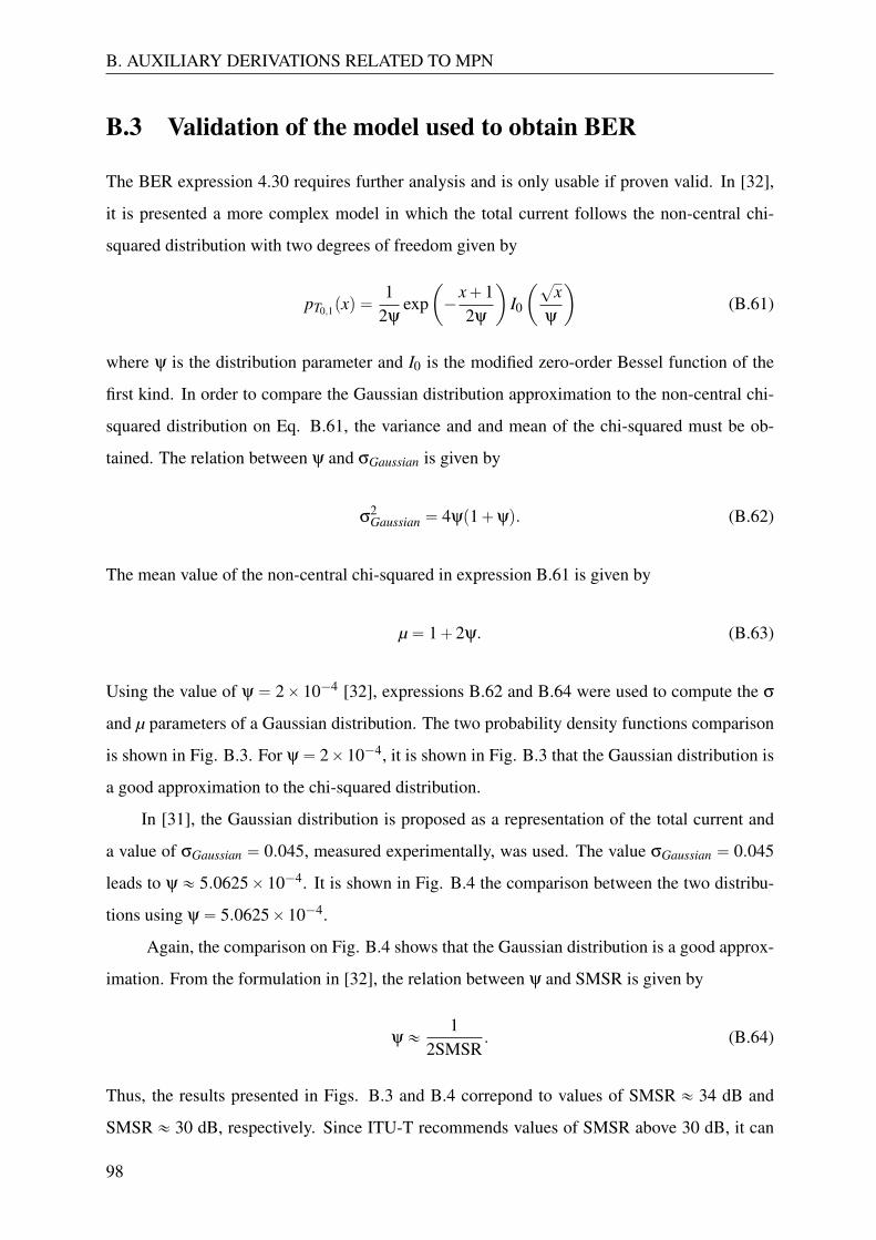
B. AUXILIARY DERIVATIONS RELATED TO MPN
B.3 Validation of the model used to obtain BER
The BER expression 4.30 requires further analysis and is only usable if proven valid. In [32],
it is presented a more complex model in which the total current follows the non-central chi-
squared distribution with two degrees of freedom given by
pT0,1pxq “1
2ψexp
ˆ
´x`12ψ
˙
I0
ˆ?x
ψ
˙
(B.61)
where ψ is the distribution parameter and I0 is the modified zero-order Bessel function of the
first kind. In order to compare the Gaussian distribution approximation to the non-central chi-
squared distribution on Eq. B.61, the variance and and mean of the chi-squared must be ob-
tained. The relation between ψ and σGaussian is given by
σ2Gaussian “ 4ψp1`ψq. (B.62)
The mean value of the non-central chi-squared in expression B.61 is given by
µ“ 1`2ψ. (B.63)
Using the value of ψ “ 2ˆ10´4 [32], expressions B.62 and B.64 were used to compute the σ
and µ parameters of a Gaussian distribution. The two probability density functions comparison
is shown in Fig. B.3. For ψ“ 2ˆ10´4, it is shown in Fig. B.3 that the Gaussian distribution is
a good approximation to the chi-squared distribution.
In [31], the Gaussian distribution is proposed as a representation of the total current and
a value of σGaussian “ 0.045, measured experimentally, was used. The value σGaussian “ 0.045
leads to ψ « 5.0625ˆ10´4. It is shown in Fig. B.4 the comparison between the two distribu-
tions using ψ“ 5.0625ˆ10´4.
Again, the comparison on Fig. B.4 shows that the Gaussian distribution is a good approx-
imation. From the formulation in [32], the relation between ψ and SMSR is given by
ψ«1
2SMSR. (B.64)
Thus, the results presented in Figs. B.3 and B.4 correpond to values of SMSR « 34 dB and
SMSR « 30 dB, respectively. Since ITU-T recommends values of SMSR above 30 dB, it can
98
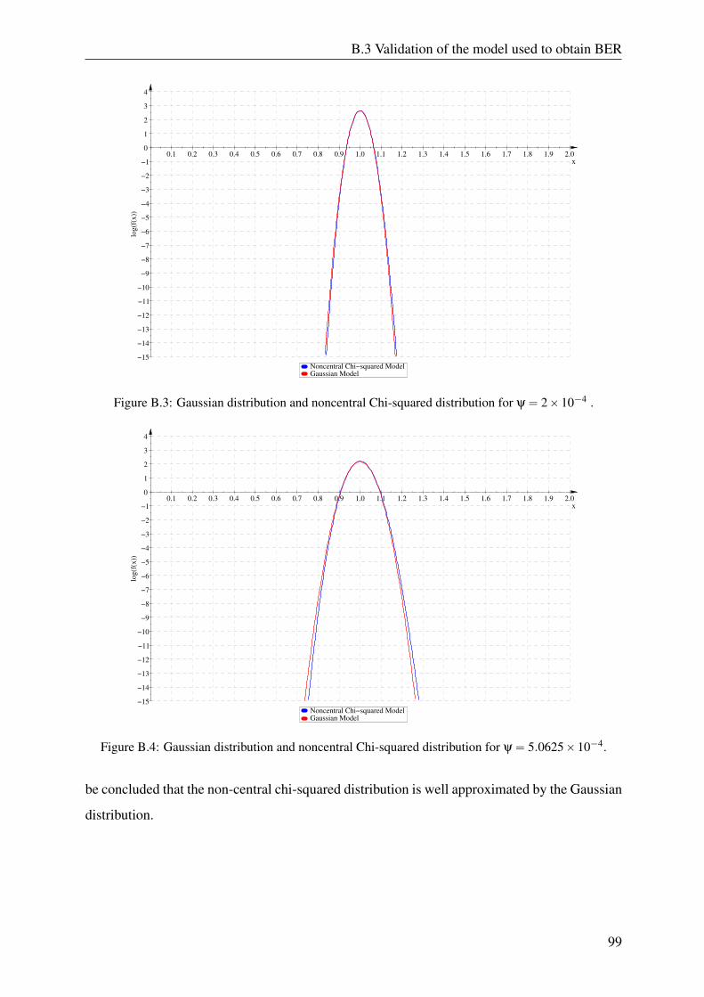
B.3 Validation of the model used to obtain BER
Noncentral Chi−squared ModelGaussian Model
0.1 0.2 0.3 0.4 0.5 0.6 0.7 0.8 0.9 1.0 1.1 1.2 1.3 1.4 1.5 1.6 1.7 1.8 1.9 2.0
−15
−14
−13
−12
−11
−10
−9
−8
−7
−6
−5
−4
−3
−2
−1
0
1
2
3
4
x
log(f
(x))
Figure B.3: Gaussian distribution and noncentral Chi-squared distribution for ψ“ 2ˆ10´4 .
Noncentral Chi−squared ModelGaussian Model
0.1 0.2 0.3 0.4 0.5 0.6 0.7 0.8 0.9 1.0 1.1 1.2 1.3 1.4 1.5 1.6 1.7 1.8 1.9 2.0
−15
−14
−13
−12
−11
−10
−9
−8
−7
−6
−5
−4
−3
−2
−1
0
1
2
3
4
x
log(f
(x))
Figure B.4: Gaussian distribution and noncentral Chi-squared distribution for ψ“ 5.0625ˆ10´4.
be concluded that the non-central chi-squared distribution is well approximated by the Gaussian
distribution.
99