Embed Size (px)
Citation preview
US 20020117697A1
(12) Patent Application Publication (10) Pub. No.: US 2002/0117697 A1 (19) United States
Tanaka et al. (43) Pub. Date: Aug. 29, 2002
(54) AVALANCHE PHOTO-DIODE AND FABRICATION METHOD THEREOF
(76) Inventors: Shigehisa Tanaka, Kunitachi (JP); Yasunobu Matsuoka, Hachioji (JP); Kazuhiro Ito, Hinode (JP); Tomohiro Ohno, Hachioji (JP); Sumiko Fujisaki, Hachioji (JP); Akira Taike, Kokubunji (JP); Tsukuru Ohtoshi, Hanno (JP); Shinji Tsuji, Hidaka (JP)
Correspondence Address: ANTONELLI TERRY STOUT AND KRAUS SUITE 1800 1300 NORTH SEVENTEENTH STREET ARLINGTON, VA 22209
(21) Appl. No.: 09/942,737
(22) Filed: Aug. 31, 2001
(30) Foreign Application Priority Data
Feb. 26, 2001 (JP) 2001-050054 Jun. 12, 2001 (JP) .................................... .. 2001-176738
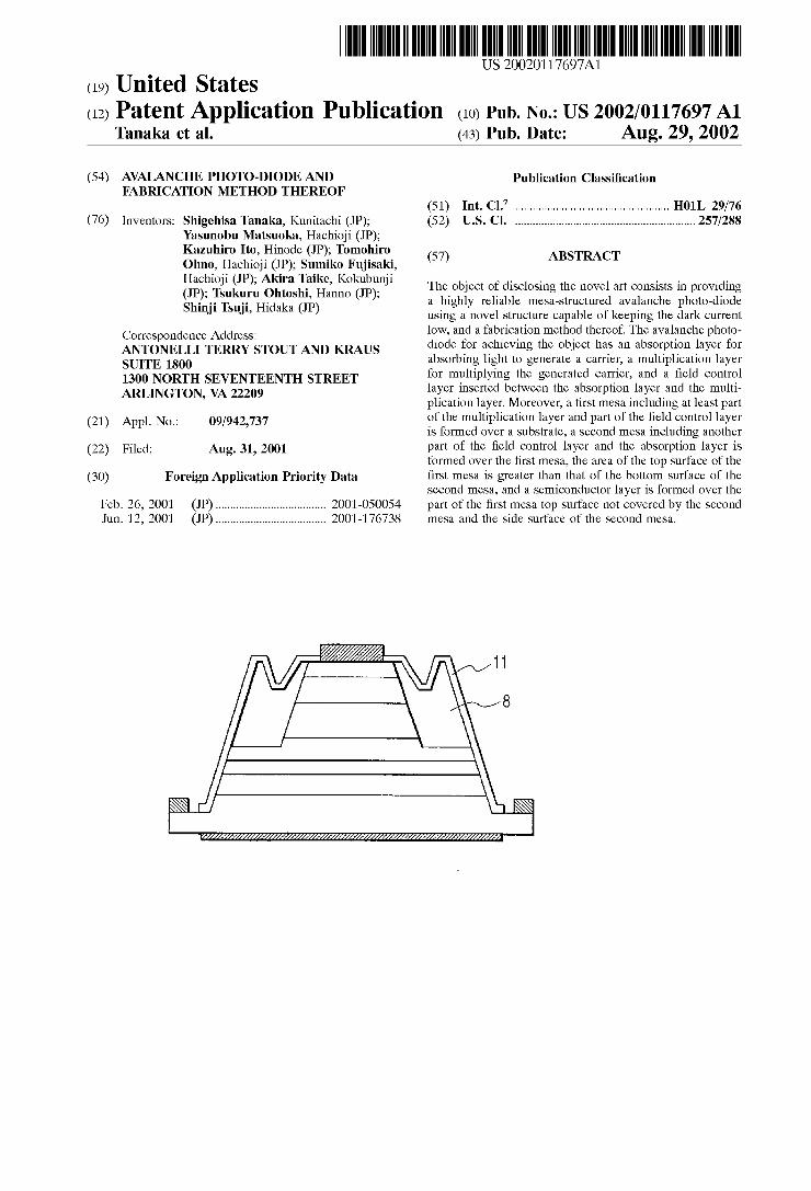
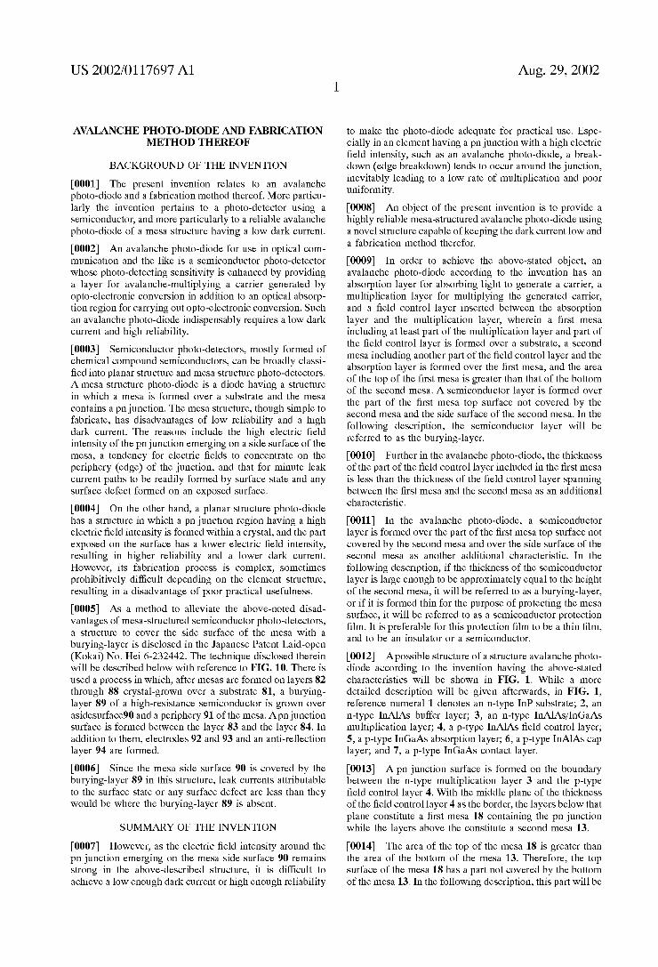
Publication Classi?cation
(51) Int. Cl? ................................................... ..H01L 29/76 (52) Us. 01. ............................................................ ..257/288
(57) ABSTRACT
The object of disclosing the novel art consists in providing a highly reliable mesa-structured avalanche photo-diode using a novel structure capable of keeping the dark current loW, and a fabrication method thereof. The avalanche photo diode for achieving the object has an absorption layer for absorbing light to generate a carrier, a multiplication layer for multiplying the generated carrier, and a ?eld control layer inserted betWeen the absorption layer and the multi plication layer. Moreover, a ?rst mesa including at least part of the multiplication layer and part of the ?eld control layer is formed over a substrate, a second mesa including another part of the ?eld control layer and the absorption layer is formed over the ?rst mesa, the area of the top surface of the ?rst mesa is greater than that of the bottom surface of the second mesa, and a semiconductor layer is formed over the part of the ?rst mesa top surface not covered by the second mesa and the side surface of the second mesa.
Patent Application Publication Aug. 29, 2002 Sheet 1 0f 15 US 2002/0117697 A1
FIG. 1
MESA QENTER MESA PEIRIPHERY '
i 10 11 i 1 1
14 ‘a _________ __
\ i //I’/ W‘ '
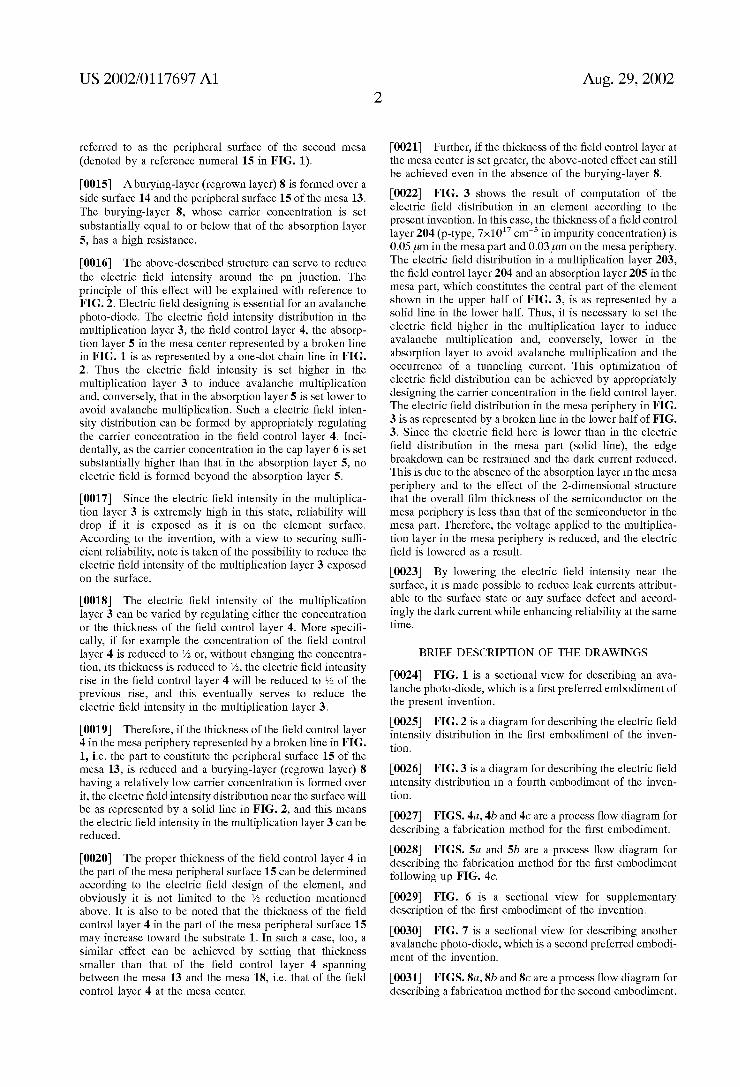
15 16 7/
\
Patent Application Publication Aug. 29, 2002 Sheet 3 0f 15 US 2002/0117697 A1
/ CENTER CENTER IN MESA (N MESA PERTPHERY CENTER
5 i 211
206
205
204 203
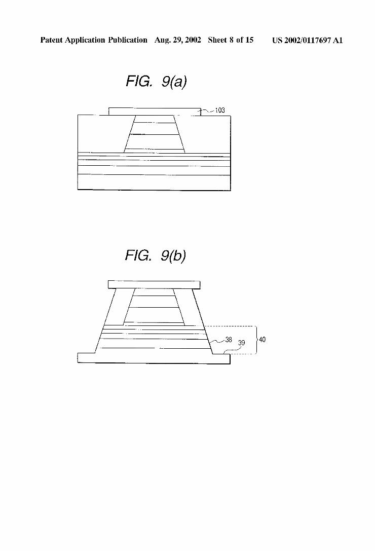
/5 £202 210w§ , g g 210 a j 201
I‘ MESA CENTER T MESA MESA PERIPHERY PERTPRERY
FIELD CCNTRCL LAYER (MESA CENTER) FIELD CONTROL LAYER ABSORPTTON LAYER (MESA PERIPHERY) (MESA CENTER)
MULTIPLICATION LAYER-/\ A|R (MESA PERIPHERY)
1000 CENTER (N MESA A "_ CENTER
5 800 — ______ __ CENTER IN MESA i PERIPHERY ‘5’ 600 ~ |J__J
E 400 -
E --------- A as 200 — -\
\l 4/3 “"“f' - _ _ _ - - - _ "'_"i"—--_T--_""(\ "-_-" O l \
0 0.2 0.4 0.6 ’ 1.42
THICKNESS ( u m)
Patent Application Publication Aug. 29, 2002 Sheet 4 0f 15 US 2002/0117697 A1
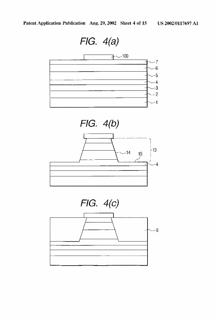
FIG. 4(a)
AIUOO-P-U‘IOUN FIG. 4(0)
FIG. 4(0)
Patent Application Publication Aug. 29, 2002 Sheet 5 0f 15 US 2002/0117697 A1
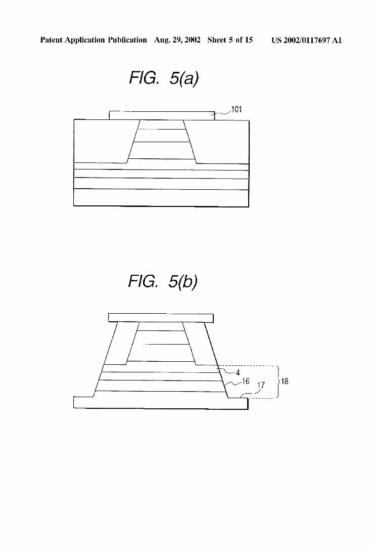
FIG. 5(a) 101
FIG. 5(b)
Patent Application Publication Aug. 29, 2002 Sheet 6 0f 15 US 2002/0117697 A1
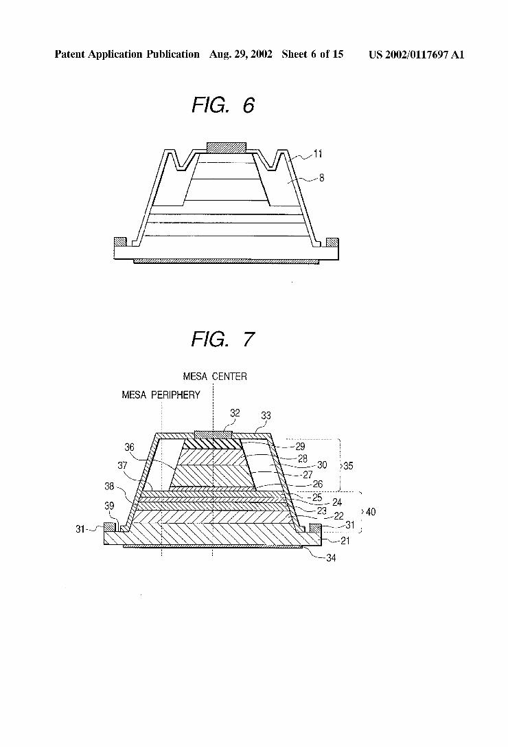
WM/Jwmmmm/mmmImmMv/m
FIG. 7
MESA CENTER
MESA PERIPHERY
E 32 33
\\\\\\\m\\\\\\\ _______________ _, - ‘_\ 36 I i \ 29 37 g V \\ 28 30 85
..- 2 ‘ \ 27 Q‘ = , ‘ 26
~ * > 5 ____ 23 22
38
39 \
will: IIIIIIIIIIIIIIIIIIIA
Patent Application Publication Aug. 29, 2002 Sheet 7 0f 15 US 2002/0117697 A1
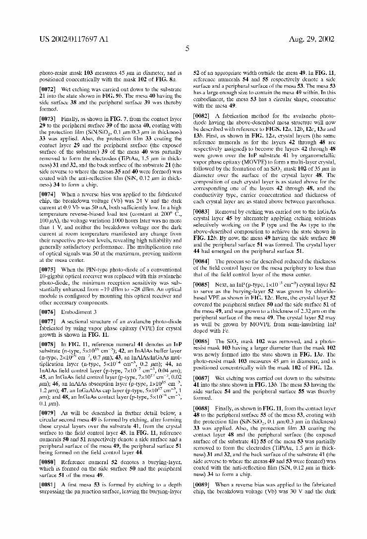
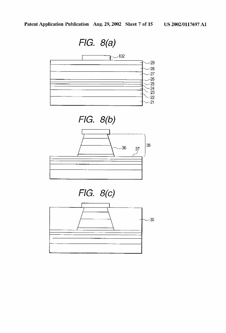
FIG. 8(a) 102
FIG. 8(b)
FIG. 8(0)
Patent Application Publication Aug. 29, 2002 Sheet 8 0f 15 US 2002/0117697 A1
FIG. 9(a)
FIG. 9(1))
Patent Application Publication Aug. 29, 2002 Sheet 9 0f 15 US 2002/0117697 A1
\\\\\\\\\\\\\\\\\
<"" III M \\\\\\\\\\\\\\\\\\\‘ YIIIIIIIIIIIIIIIIIIIIIIIIIIIIIIIIIIIIIIIIIIllIIIIIIIIIIIIIIIIIIIIIIIIIIIIIIIIIIIA
7%
FIG. 11
MESA MESA PERIPHERY CENTER
5 i 33
5() ”<7\""*% ______________________________ n
i . '4. 422 54 i l 425
\ \ - 55 - v 44 / A ; 43 53 \f\\ "0' 42
31 i 4 u ,,,,,, = [IA 41 \\\\\\\\\\\\\\\\\\\\\\\\\\\\\\\\\\\\\\\\\\\\\\\\\\\\\\\\\\\§
Patent Application Publication Aug. 29, 2002 Sheet 10 0f 15 US 2002/0117697 A1
FIG. 12(a) 102
FIG. 12(1))
FIG. 12(0) l___|
E “52
Patent Application Publication Aug. 29, 2002 Sheet 11 0f 15 US 2002/0117697 A1
FIG. 13(a)
FIG. 13(1)) 7 Z \ _____ Us; ______ V‘
{V 55 53 F4 1
Patent Application Publication Aug. 29, 2002 Sheet 12 0f 15 US 2002/0117697 A1
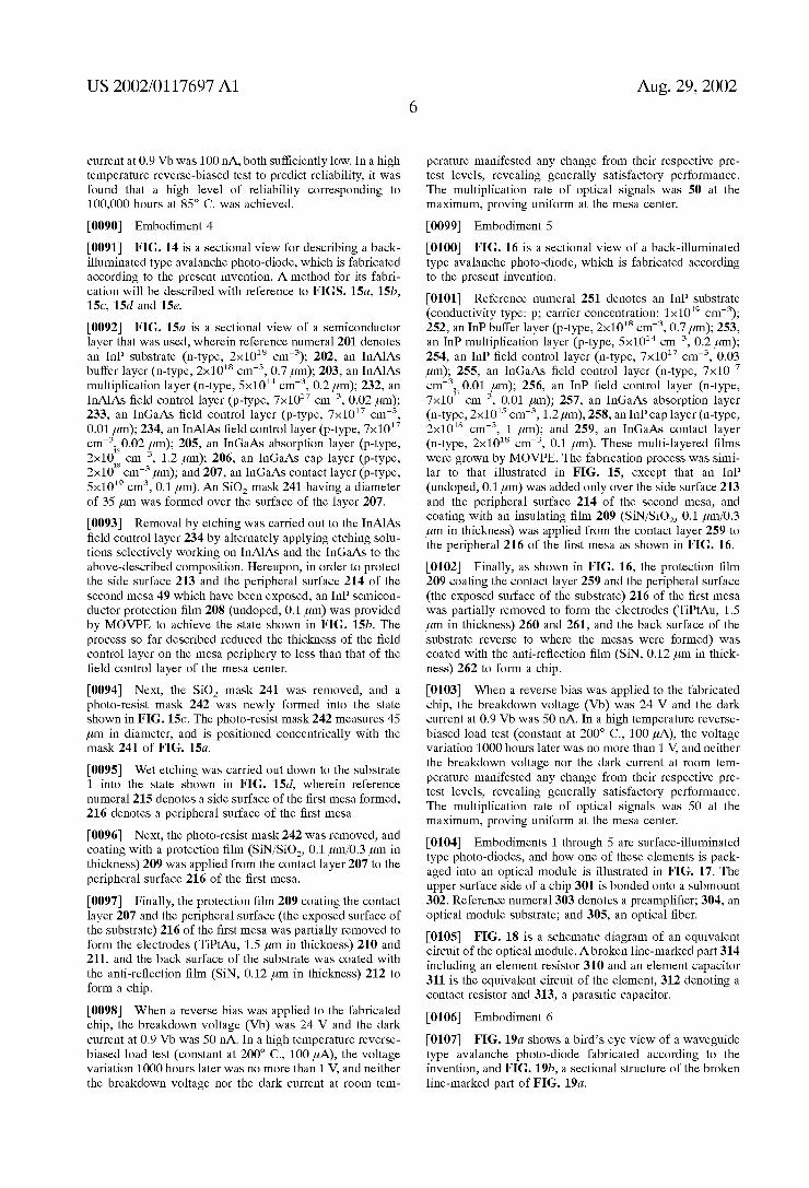
FIG. 15(a)
Patent Application Publication Aug. 29, 2002 Sheet 13 0f 15 US 2002/0117697 A1
FIG. 16
Patent Application Publication Aug. 29, 2002 Sheet 14 0f 15 US 2002/0117697 A1
FIG. 17
310
Patent Application Publication Aug. 29, 2002 Sheet 15 0f 15
FIG. 19(a)
285
284
FIG. 19(1)) 285
‘mm 284
US 2002/0117697 A1
US 2002/0117697 A1
AVALANCHE PHOTO-DIODE AND FABRICATION METHOD THEREOF
BACKGROUND OF THE INVENTION
[0001] The present invention relates to an avalanche photo-diode and a fabrication method thereof. More particu larly the invention pertains to a photo-detector using a semiconductor, and more particularly to a reliable avalanche photo-diode of a mesa structure having a loW dark current.
[0002] An avalanche photo-diode for use in optical com munication and the like is a semiconductor photo-detector Whose photo-detecting sensitivity is enhanced by providing a layer for avalanche-multiplying a carrier generated by opto-electronic conversion in addition to an optical absorp tion region for carrying out opto-electronic conversion. Such an avalanche photo-diode indispensably requires a loW dark current and high reliability.
[0003] Semiconductor photo-detectors, mostly formed of chemical compound semiconductors, can be broadly classi ?ed into planar structure and mesa structure photo-detectors. A mesa structure photo-diode is a diode having a structure in Which a mesa is formed over a substrate and the mesa
contains a pn junction. The mesa structure, though simple to fabricate, has disadvantages of loW reliability and a high dark current. The reasons include the high electric ?eld intensity of the pn junction emerging on a side surface of the mesa, a tendency for electric ?elds to concentrate on the periphery (edge) of the junction, and that for minute leak current paths to be readily formed by surface state and any surface defect formed on an eXposed surface.
[0004] On the other hand, a planar structure photo-diode has a structure in Which a pn junction region having a high electric ?eld intensity is formed Within a crystal, and the part eXposed on the surface has a loWer electric ?eld intensity, resulting in higher reliability and a loWer dark current. HoWever, its fabrication process is complex, sometimes prohibitively dif?cult depending on the element structure, resulting in a disadvantage of poor practical usefulness.
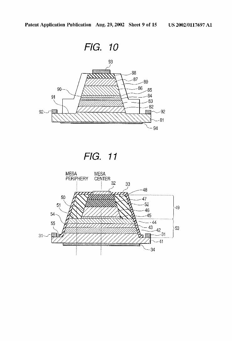
[0005] As a method to alleviate the above-noted disad vantages of mesa-structured semiconductor photo-detectors, a structure to cover the side surface of the mesa With a burying-layer is disclosed in the Japanese Patent Laid-open (Kokai) No. Hei 6-232442. The technique disclosed therein Will be described beloW With reference to FIG. 10. There is used a process in Which, after mesas are formed on layers 82 through 88 crystal-groWn over a substrate 81, a burying layer 89 of a high-resistance semiconductor is groWn over asidesurface90 and a periphery 91 of the mesa. Apn junction surface is formed betWeen the layer 83 and the layer 84. In addition to them, electrodes 92 and 93 and an anti-re?ection layer 94 are formed.
[0006] Since the mesa side surface 90 is covered by the burying-layer 89 in this structure, leak currents attributable to the surface state or any surface defect are less than they Would be Where the burying-layer 89 is absent.
SUMMARY OF THE INVENTION
[0007] HoWever, as the electric ?eld intensity around the pn junction emerging on the mesa side surface 90 remains strong in the above-described structure, it is difficult to achieve a loW enough dark current or high enough reliability
Aug. 29, 2002
to make the photo-diode adequate for practical use. Espe cially in an element having a pn junction With a high electric ?eld intensity, such as an avalanche photo-diode, a break doWn (edge breakdoWn) tends to occur around the junction, inevitably leading to a loW rate of multiplication and poor uniformity. [0008] An object of the present invention is to provide a highly reliable mesa-structured avalanche photo-diode using a novel structure capable of keeping the dark current loW and a fabrication method therefor.
[0009] In order to achieve the above-stated object, an avalanche photo-diode according to the invention has an absorption layer for absorbing light to generate a carrier, a multiplication layer for multiplying the generated carrier, and a ?eld control layer inserted betWeen the absorption layer and the multiplication layer, Wherein a ?rst mesa including at least part of the multiplication layer and part of the ?eld control layer is formed over a substrate, a second mesa including another part of the ?eld control layer and the absorption layer is formed over the ?rst mesa, and the area of the top of the ?rst mesa is greater than that of the bottom of the second mesa. A semiconductor layer is formed over the part of the ?rst mesa top surface not covered by the second mesa and the side surface of the second mesa. In the folloWing description, the semiconductor layer Will be referred to as the burying-layer.
[0010] Further in the avalanche photo-diode, the thickness of the part of the ?eld control layer included in the ?rst mesa is less than the thickness of the ?eld control layer spanning betWeen the ?rst mesa and the second mesa as an additional characteristic.
[0011] In the avalanche photo-diode, a semiconductor layer is formed over the part of the ?rst mesa top surface not covered by the second mesa and over the side surface of the second mesa as another additional characteristic. In the folloWing description, if the thickness of the semiconductor layer is large enough to be approximately equal to the height of the second mesa, it Will be referred to as a burying-layer, or if it is formed thin for the purpose of protecting the mesa surface, it Will be referred to as a semiconductor protection ?lm. It is preferable for this protection ?lm to be a thin ?lm, and to be an insulator or a semiconductor.
[0012] Apossible structure of a structure avalanche photo diode according to the invention having the above-stated characteristics Will be shoWn in FIG. 1. While a more detailed description Will be given afterWards, in FIG. 1, reference numeral 1 denotes an n-type InP substrate; 2, an n-type InAlAs buffer layer; 3, an n-type InAlAs/InGaAs multiplication layer; 4, a p-type InAlAs ?eld control layer; 5, a p-type InGaAs absorption layer; 6, a p-type InAlAs cap layer; and 7, a p-type InGaAs contact layer.
[0013] A pn junction surface is formed on the boundary betWeen the n-type multiplication layer 3 and the p-type ?eld control layer 4. With the middle plane of the thickness of the ?eld control layer 4 as the border, the layers beloW that plane constitute a ?rst mesa 18 containing the pn junction While the layers above the constitute a second mesa 13.
[0014] The area of the top of the mesa 18 is greater than the area of the bottom of the mesa 13. Therefore, the top surface of the mesa 18 has a part not covered by the bottom of the mesa 13. In the folloWing description, this part Will be
US 2002/0117697 A1
referred to as the peripheral surface of the second mesa (denoted by a reference numeral 15 in FIG. 1).
[0015] Aburying-layer (regroWn layer) 8 is formed over a side surface 14 and the peripheral surface 15 of the mesa 13. The burying-layer 8, Whose carrier concentration is set substantially equal to or beloW that of the absorption layer 5, has a high resistance.
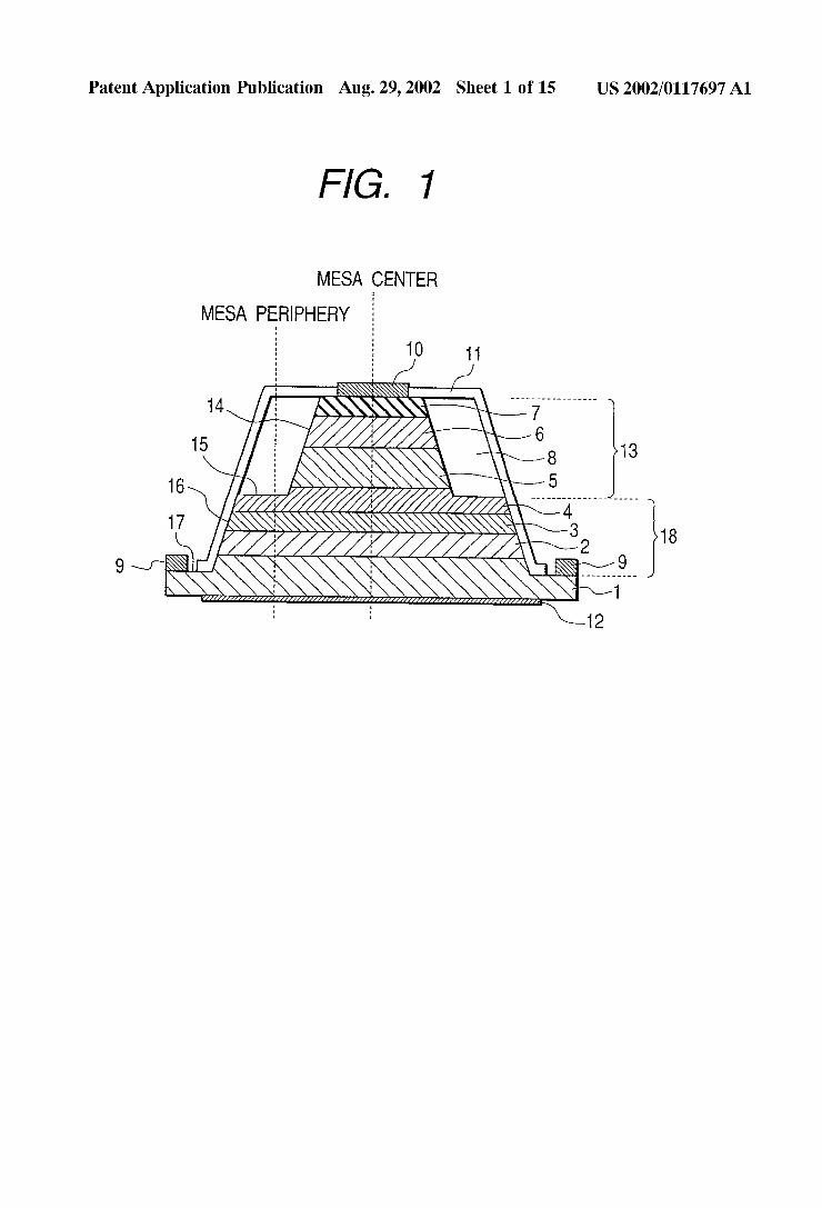
[0016] The above-described structure can serve to reduce the electric ?eld intensity around the pn junction. The principle of this effect Will be explained With reference to FIG. 2. Electric ?eld designing is essential for an avalanche photo-diode. The electric ?eld intensity distribution in the multiplication layer 3, the ?eld control layer 4, the absorp tion layer 5 in the mesa center represented by a broken line in FIG. 1 is as represented by a one-dot chain line in FIG. 2. Thus the electric ?eld intensity is set higher in the multiplication layer 3 to induce avalanche multiplication and, conversely, that in the absorption layer 5 is set loWer to avoid avalanche multiplication. Such a electric ?eld inten sity distribution can be formed by appropriately regulating the carrier concentration in the ?eld control layer 4. Inci dentally, as the carrier concentration in the cap layer 6 is set substantially higher than that in the absorption layer 5, no electric ?eld is formed beyond the absorption layer 5.
[0017] Since the electric ?eld intensity in the multiplica tion layer 3 is extremely high in this state, reliability Will drop if it is eXposed as it is on the element surface. According to the invention, With a vieW to securing suf? cient reliability, note is taken of the possibility to reduce the electric ?eld intensity of the multiplication layer 3 exposed on the surface.
[0018] The electric ?eld intensity of the multiplication layer 3 can be varied by regulating either the concentration or the thickness of the ?eld control layer 4. More speci? cally, if for eXample the concentration of the ?eld control layer 4 is reduced to 1/2 or, Without changing the concentra tion, its thickness is reduced to 1/2, the electric ?eld intensity rise in the ?eld control layer 4 Will be reduced to 1/2 of the previous rise, and this eventually serves to reduce the electric ?eld intensity in the multiplication layer 3.
[0019] Therefore, if the thickness of the ?eld control layer 4 in the mesa periphery represented by a broken line in FIG. 1, i.e. the part to constitute the peripheral surface 15 of the mesa 13, is reduced and a burying-layer (regroWn layer) 8 having a relatively loW carrier concentration is formed over it, the electric ?eld intensity distribution near the surface Will be as represented by a solid line in FIG. 2, and this means the electric ?eld intensity in the multiplication layer 3 can be reduced.
[0020] The proper thickness of the ?eld control layer 4 in the part of the mesa peripheral surface 15 can be determined according to the electric ?eld design of the element, and obviously it is not limited to the 1/2 reduction mentioned above. It is also to be noted that the thickness of the ?eld control layer 4 in the part of the mesa peripheral surface 15 may increase toWard the substrate 1. In such a case, too, a similar effect can be achieved by setting that thickness smaller than that of the ?eld control layer 4 spanning betWeen the mesa 13 and the mesa 18, i.e. that of the ?eld control layer 4 at the mesa center.
Aug. 29, 2002
[0021] Further, if the thickness of the ?eld control layer at the mesa center is set greater, the above-noted effect can still be achieved even in the absence of the burying-layer 8.
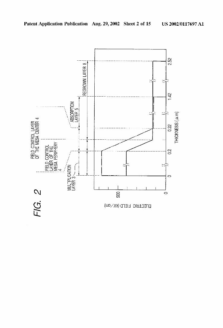
[0022] FIG. 3 shoWs the result of computation of the electric ?eld distribution in an element according to the present invention. In this case, the thickness of a ?eld control layer 204 (p-type, 7><1017 cm'3 in impurity concentration) is 0.05 pm in the mesa part and 0.03 pm on the mesa periphery. The electric ?eld distribution in a multiplication layer 203, the ?eld control layer 204 and an absorption layer 205 in the mesa part, Which constitutes the central part of the element shoWn in the upper half of FIG. 3, is as represented by a solid line in the loWer half. Thus, it is necessary to set the electric ?eld higher in the multiplication layer to induce avalanche multiplication and, conversely, loWer in the absorption layer to avoid avalanche multiplication and the occurrence of a tunneling current. This optimiZation of electric ?eld distribution can be achieved by appropriately designing the carrier concentration in the ?eld control layer. The electric ?eld distribution in the mesa periphery in FIG. 3 is as represented by a broken line in the loWer half of FIG. 3. Since the electric ?eld here is loWer than in the electric ?eld distribution in the mesa part (solid line), the edge breakdoWn can be restrained and the dark current reduced. This is due to the absence of the absorption layer in the mesa periphery and to the effect of the 2-dimensional structure that the overall ?lm thickness of the semiconductor on the mesa periphery is less than that of the semiconductor in the mesa part. Therefore, the voltage applied to the multiplica tion layer in the mesa periphery is reduced, and the electric ?eld is loWered as a result.
[0023] By loWering the electric ?eld intensity near the surface, it is made possible to reduce leak currents attribut able to the surface state or any surface defect and accord ingly the dark current While enhancing reliability at the same time.
BRIEF DESCRIPTION OF THE DRAWINGS
[0024] FIG. 1 is a sectional vieW for describing an ava lanche photo-diode, Which is a ?rst preferred embodiment of the present invention.
[0025] FIG. 2 is a diagram for describing the electric ?eld intensity distribution in the ?rst embodiment of the inven tion.
[0026] FIG. 3 is a diagram for describing the electric ?eld intensity distribution in a fourth embodiment of the inven tion.
[0027] FIGS. 4a, 4b and 4c are a process How diagram for describing a fabrication method for the ?rst embodiment.
[0028] FIGS. 5a and 5b are a process How diagram for describing the fabrication method for the ?rst embodiment folloWing up FIG. 4c.
[0029] FIG. 6 is a sectional vieW for supplementary description of the ?rst embodiment of the invention.
[0030] FIG. 7 is a sectional vieW for describing another avalanche photo-diode, Which is a second preferred embodi ment of the invention.
[0031] FIGS. 8a, 8b and 8c are a process How diagram for describing a fabrication method for the second embodiment.
US 2002/0117697 A1
[0032] FIGS. 9a and 9b are a process How diagram for describing the fabrication method for the second embodi ment following up FIG. 8c.
[0033] FIG. 10 is a sectional vieW for describing another avalanche photo-diode, Which is an embodiment of the prior art.
[0034] FIG. 11 is a sectional vieW for describing another avalanche photo-diode, Which is a third preferred embodi ment of the invention.
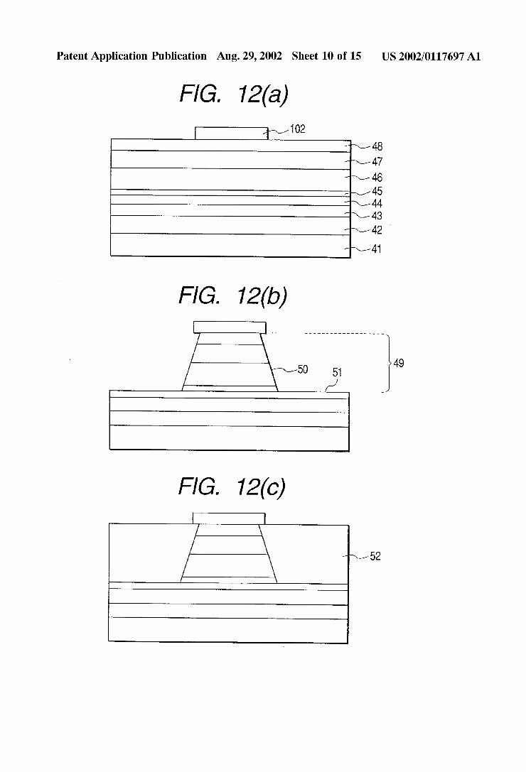
[0035] FIGS. 12a, 12b and 12c are a process How diagram for describing a fabrication method for the third embodi ment.
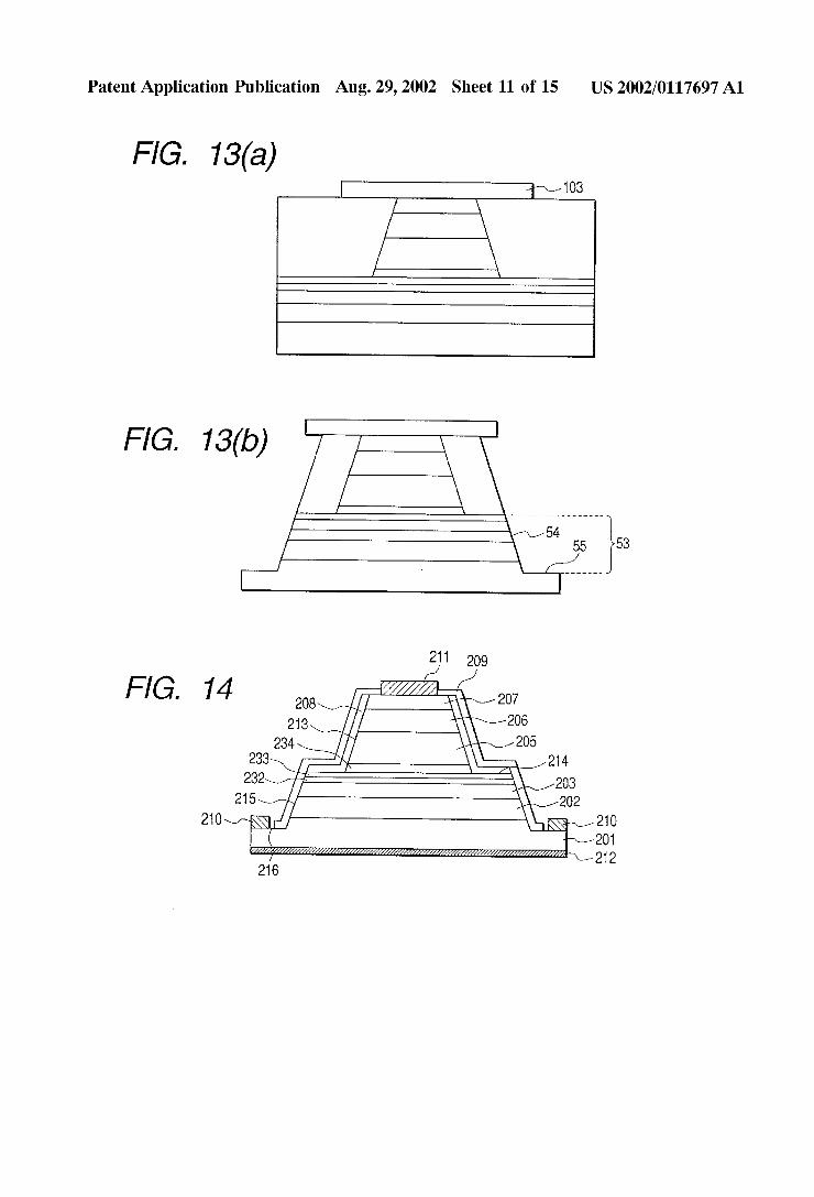
[0036] FIGS. 13a and 13b are a process How diagram for describing the fabrication method for the third embodiment folloWing up FIG. 12c.
[0037] FIG. 14 is a sectional vieW for describing another avalanche photo-diode, Which is a fourth preferred embodi ment of the invention.
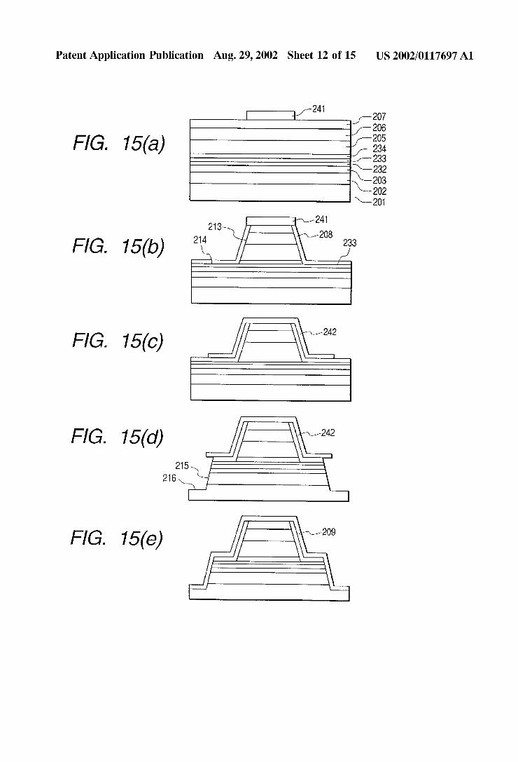
[0038] FIGS. 15a, 15b, 15c, 15d and 156 are a process How diagram for describing a fabrication method for the fourth embodiment.
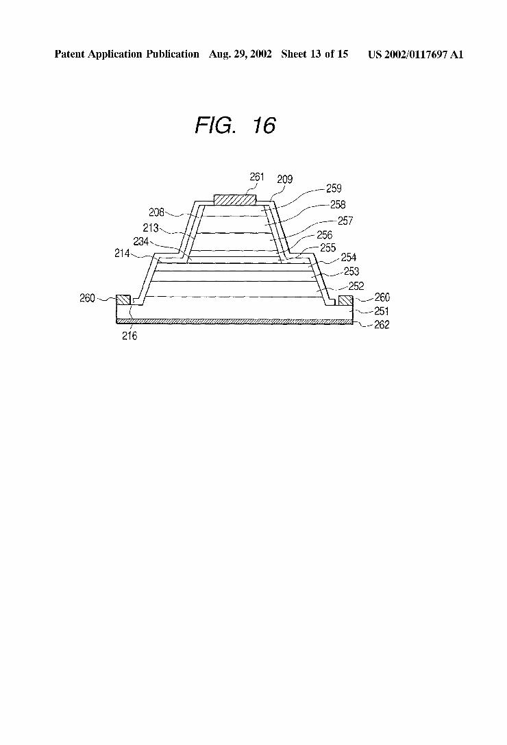
[0039] FIG. 16 is a sectional vieW for describing still another avalanche photo-diode, Which is a ?fth preferred embodiment of the invention.
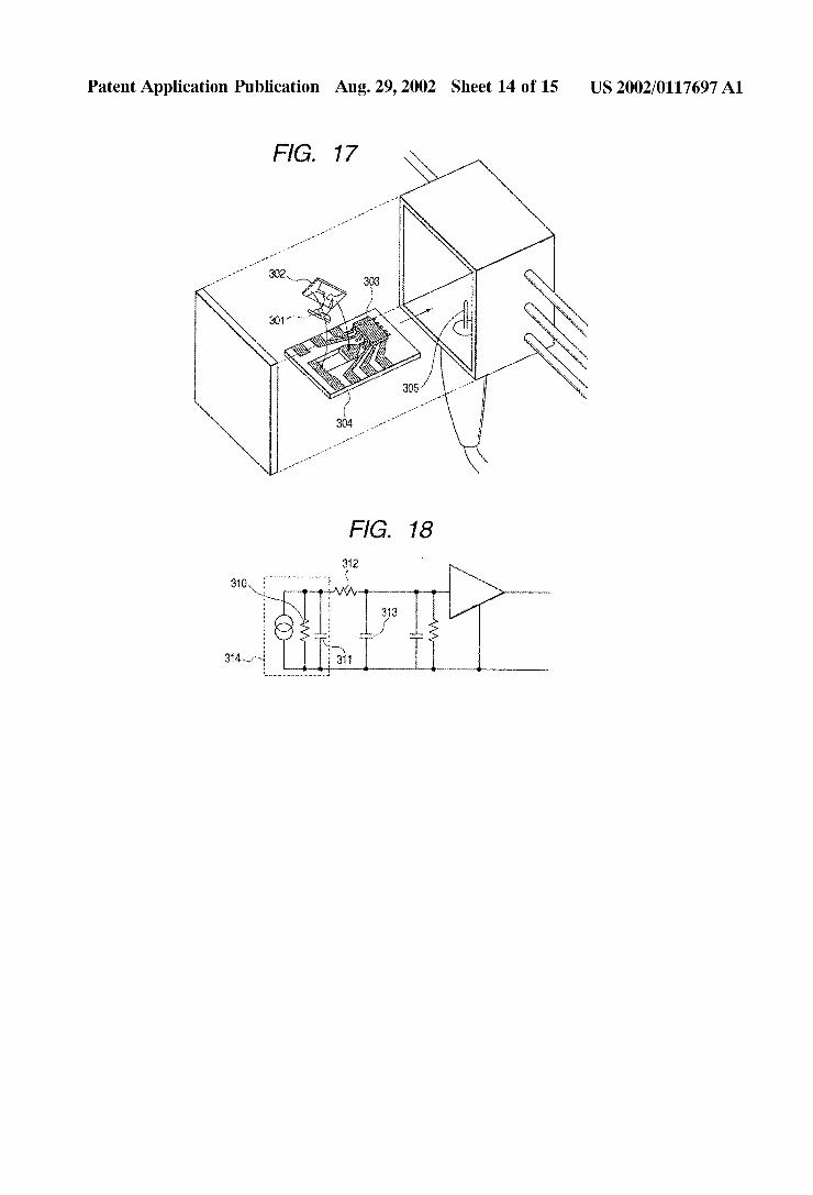
[0040] FIG. 17 illustrates hoW an optical module accord ing to the invention is packaged.
[0041] FIG. 18 is a schematic diagram of an equivalent circuit of the optical module according to the invention.
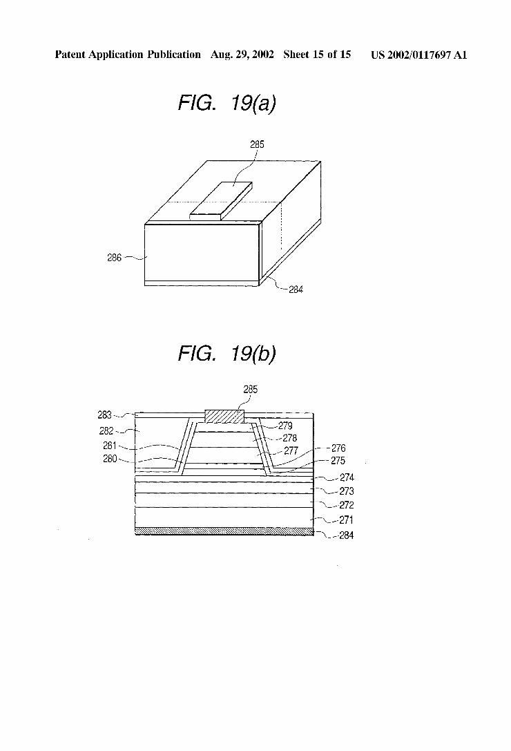
[0042] FIG. 19a is a bird’s eye vieW for describing still another avalanche photo-diode, Which is a siXth preferred embodiment of the invention.
[0043] FIG. 19b is a sectional vieW for describing the avalanche photo-diode shoWn in FIG. 19a.
DESCRIPTION OF THE PREFERRED EMBODIMENTS
[0044] Avalanche photo-diodes and fabrication methods thereof according to the present invention Will be described in further detail beloW With reference to illustrated preferred embodiments thereof.
[0045] Embodiment 1
[0046] FIG. 1 illustrates a section of the structure of the avalanche photo-diode, Which is Embodiment 1 of the invention. In FIG. 1, With the conductivity type, carrier concentration and thickness of each layer being indicated betWeen parentheses, reference numeral 1 denotes an InP substrate (n-type, 1><1019 cm_3); 2, an InAlAs buffer layer (n-type, 2><1018 cm_3, 0.7 pm); 3, an InAlAs/InGaAs mul tiplication layer (n-type, 5x1014 cm_3, 0.2 pm); 4, an InAlAs ?eld control layer (p-type, 7><1017 cm_3, 0.02 pm); 5, an InGaAs absorption layer (p-type, 2><1015 cm_3, 1.2 pm); 6, an InAlAs cap layer (p-type, 2><1018 cm_3, 1 pm); and 7, an InGaAs contact layer (p-type, 5x10¹⁹ “'3, 0.1 pm).
[0047] As Will be described in further detail beloW, the second mesa 13 is formed by etching, after forming these crystal layers over the substrate 1, from the crystal surface to midWay of the ?eld control layer 4. Whereas the shape of
Aug. 29, 2002
the mesa 13 can be chosen as preferable out of a circle, oval, rectangle, stripe or branch type, it is a circle in this embodi ment. In FIG. 1, reference numerals 14 and 15 respectively denote a side surface and a peripheral surface of the mesa 13, the peripheral surface 15 being formed on the ?eld control layer 4.
[0048] Reference numeral 8 denotes a burying-layer, Which is formed on the side surface 14 and the peripheral surface 15 of the mesa 13. The carrier concentration of the burying-layer 8, Which should preferably be not higher than that of the absorption layer 5, is 1><1014 m“3 of the p-type in this embodiment. The burying-layer 8, Which should pref erably have a suf?cient thickness for the layer to reach a higher position than the absorption layer 5 on the peripheral surface 15 of the mesa 13, is 2.31 pm thick in this embodi ment, a suf?cient thickness to let the burying-layer 8 reach the cap layer 7.
[0049] The ?rst mesa 18 is formed by etching to a depth crossing the pn junction surface (the boundary betWeen the multiplication layer 3 and the ?eld control layer 4), leaving the burying-layer 8 of an appropriate Width outside the mesa 13. In FIG. 1, reference numerals 16 and 17 respectively denote a side surface and a peripheral surface of the mesa 18. Whereas the shape of the mesa 18 can be chosen as preferable out of a circle, oval, rectangle, stripe or branch type, it has to be large enough to contain the mesa 13 Within. In the embodiment illustrated in FIG. 1, the mesa 18 has a circular shape, concentric With the mesa 13.
[0050] The pn junction surface emerges on the side sur face 16 of the mesa 18. The peripheral surface 17 of the mesa 18 may only be in a position deeper than the pn junction surface, and in this particular embodiment reaches the substrate 1. The side surface 16 of the mesa 18 and the surface of the burying-layer 8 are coated With a protection ?lm 11. Further, an electrode 10 is provided over the surface of the contact layer 7, another electrode 9 on the bottom surface 17 (the peripheral surface 17) of the mesa 18, and an anti-re?ection ?lm 12 on the back side of the substrate 1. Whether to provide a protection ?lm and an anti-re?ection ?lm and their types, if they are to be provided, and the types and positions of the electrodes can be freely selected accord ing to the pertinent requirements.
[0051] A fabrication method for the avalanche photo diode having the above-described mesa structure Will noW be described With reference to FIGS. 4a, 4b, 4c, 5a and 5b. First, as shoWn in FIG. 4a, crystal layers 2 through 7 (the same reference numerals as for the layers 2 through 7 are respectively assigned) to become the layers 2 through 7 Were groWn over the InP substrate 1 by molecular beam epitaXy (MBE) to form a multi-layer crystal, folloWed by the for mation of an SiO2 mask 100 of 35 pm in diameter over the surface of the crystal layer 7. The composition, conductivity type, carrier concentration and thickness of each crystal layer Were as stated above.
[0052] Then, Wet etching Was carried out for removal to midWay of the crystal layer 4 to achieve the state of FIG. 4b. By noW, the side surface 14 and the peripheral surface 15 of the mesa 13 Were formed. The crystal layer 4 had emerged on the peripheral surface 15.
[0053] The process so far described reduced the thickness of the ?eld control layer 4 on the mesa periphery to less than that of the ?eld control layer 4 of the mesa center.
US 2002/0117697 A1
[0054] Next, an InAlAs (p-type, 1><1014 cm_3) crystal layer 8 to serve as the burying-layer 8 was grown by MBE into the state shown in FIG. 4c. Here, the crystal layer 8 covered the peripheral surface 15 and the side surface 14 of the mesa 13, and was grown to a thickness of 2.31 pm on the peripheral surface 15 of the mesa 13.
[0055] The SiO2 mask 100 was removed, and a photo resist mask 101 having a larger diameter than the mask 100 was newly formed into the state shown in FIG. 5a. The photo-resist mask 101 measures 45 pm in diameter, and is positioned concentrically with the mask 100 of FIG. 4a.
[0056] Wet etching was carried out down to the substrate 1 into the state shown in FIG. 5b. The mesa 18 having the side surface 16 and the peripheral surface 17 was thereby formed.
[0057] Finally, as shown in FIG. 1, from the contact layer 7 to the peripheral surface 17 of the mesa 18, coating with the protection ?lm (SiN/SiO2, 0.1 pm/0.3 pm in thickness) 11 was applied. Also, the protection ?lm 11 coating the contact layer 7 and the peripheral surface (the eXposed surface of the substrate) 17 of the mesa 18 was partially removed to form the electrodes (TiPtAu, 1.5 pm in thick ness) 9 and 10, and the back surface of the substrate 1 (the side reverse to where the mesas 13 and 18 were formed) was coated with the anti-re?ection ?lm (SiN, 0.12 pm in thick ness) 12 to form a chip.
[0058] When a reverse bias was applied to the fabricated chip, the breakdown voltage was 24 V and the dark current at 0.9 Vb was 50 nA, both suf?ciently low. In a high temperature reverse-biased load test (constant at 200° C., 100 MA), the voltage variation 1000 hours later was no more than 1 V, and neither the breakdown voltage nor the dark current at room temperature manifested any change from their respective pre-test levels, revealing high reliability and generally satisfactory performance. The multiplication rate of optical signals was 50 at the maXimum, proving uniform at the mesa center.
[0059] Further, as shown in FIG. 6, similar element per formance was observed of a chip of which the top surface of the burying-layer 8 was not ?at, demonstrating that the characteristics of this element were not dependent on the shape of the burying-layer.
[0060] Embodiment 2
[0061] Since the ?eld control layer of an avalanche photo diode is as thin as about 0.05 pm, it is sometimes dif?cult to stop etching midway of the ?eld control layer. A sectional structure of an avalanche photo-diode used in such a case is illustrated in FIG. 7.
[0062] In FIG. 7, reference numeral 21 denotes an InP substrate (n-type, 1><1019 cm_3); 22, an InAlAs buffer layer (n-type, 2><1018 cc_3, 0.7 pm); 23, an InAlAs/InGaAs mul tiplication layer (n-type, 5><1014 cm_3, 0.2 pm); 24, an InAlAs ?eld control layer (p-type, 7><1017 cm_3, 0.02 pm); 25, an InGaAs ?eld control layer (p-type, 7><1017 cm_3, 0.01 pm); 26, an InAlAs ?eld control layer (p-type, 7><1017 cm_3, 0.02 pm); 27, an InGaAs absorption layer (p-type, 2><1015 cm_3, 1.2 pm); 28, an InGaAlAs cap layer (p-type, 2><1018 cm‘319 1 pm);and 29, an InGaAs contact layer (p-type, 5x10 cm_3, 0.1 pm).
Aug. 29, 2002
[0063] As will be described in further detail below, a circular second mesa 35 is formed by etching, after forming these crystal layers over the substrate 21, from the crystal surface to the ?eld control layer 26. In FIG. 7, reference numerals 36 and 37 respectively denote a side surface and a peripheral surface of the mesa 35, the peripheral surface 37 being formed on the ?eld control layer 25.
[0064] Reference numeral 30 denotes a burying-layer, which is formed on the side surface 36 and the peripheral surface 37 of the mesa 35.
[0065] A ?rst mesa 40 is formed by etching to a depth crossing the pn junction surface (the boundary between the multiplication layer 23 and the ?eld control layer 24) leaving the burying-layer 30 of an appropriate width outside the mesa 35. In FIG. 7, reference numerals 38 and 39 respec tively denote a side surface and a peripheral surface of the mesa 40. The mesa 40 has a large enough siZe to contain the mesa 35 within. In the embodiment illustrated in FIG. 7, the mesa 40 has a circular shape, concentric with the mesa 35.
[0066] The pn junction surface emerges on the side sur face 38 of the mesa 40. The peripheral surface 39 of the mesa 40 may only be in a position deeper than the pn junction surface, and in this particular embodiment reaches the substrate 21. The side surface 38 of the mesa 40 and the surface of the burying-layer 30 are coated with a protection ?lm 33. Further, an electrode 32 is provided over the surface of the contact layer 29, another electrode 31 on the bottom surface 39 of the mesa 40, and an anti-re?ection ?lm 34 on the back side of the substrate 21.
[0067] A fabrication method for the avalanche photo diode having the above-described mesa structure will now be described with reference to FIGS. 8a, 8b, 8c, 9a and 9b. First, as shown in FIG. 8a, crystal layers 22 through 29 (the same reference numerals as for the layers 22 through 29 are respectively assigned) to become the layers 22 through 29 were grown over the InP substrate 21 by MBE to form a multi-layer crystal, followed by the formation of an SiO2 mask 102 of 35 pm in diameter over the surface of the crystal layer 29. The composition, conductivity type, carrier con centration and thickness of each crystal layer were as stated above between parentheses.
[0068] Removal by etching was carried out to the InAlAs crystal layer 26 by alternately applying etching solutions selectively working on InAlAs and InGaAs to the above described composition to achieve the state shown in FIG. 8b. By now, the mesa 35 having the side surface 36 and the peripheral surface 37 were formed. The crystal layer 25 had emerged on the peripheral surface 37.
[0069] The process so far described reduced the thickness of the ?eld control layer on the mesa periphery to less than that of the ?eld control layer of the mesa center.
[0070] Next, an InAlAs (p-type, 1><1014 cm_3) crystal layer 30 to serve as the burying-layer 30 was grown by MBE into the state shown in FIG. 8c. Here, the crystal layer 30 covered the peripheral surface 37 and the side surface 36 of the mesa 35, and was grown to a thickness of 2.32 pm on the peripheral surface 37 of the mesa 35.
[0071] The SiO2 mask 102 was removed, and a photo resist mask 103 having a larger diameter than the mask 102 was newly formed into the state shown in FIG. 9a. The