Embed Size (px)
Citation preview
Avnet Embedded. Support Around The Board™
www.avnet-embedded.eu
AvnET EmBEddEd SpEcificATion.
datasheetSharp
LQ035Q7DH06
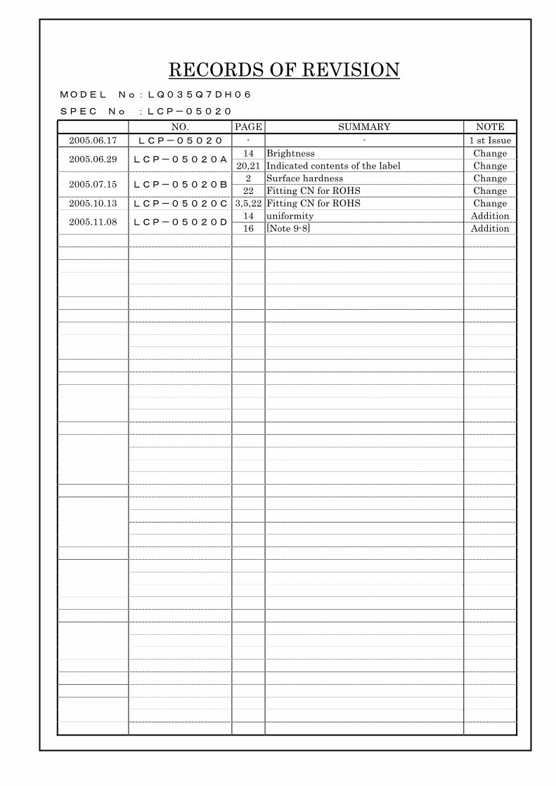
RECORDS OF REVISION MODEL No:LQ035Q7DH06
SPEC No :LCP-05020 NO. PAGE SUMMARY NOTE
2005.06.17 LCP-05020 - - 1 st Issue14 Brightness Change 2005.06.29 LCP-05020A 20,21 Indicated contents of the label Change 2 Surface hardness Change 2005.07.15 LCP-05020B 22 Fitting CN for ROHS Change
2005.10.13 LCP-05020C 3,5,22 Fitting CN for ROHS Change 14 uniformity Addition2005.11.08 LCP-05020D 16 [Note 9-8] Addition
LCP-05020-1
NOTICE This publication is the proprietary of SHARP and is copyrighted, with all rights reserved. Under the copyright laws, no part of this publication may be reproduced or transmitted in any form or by any means, electronic or mechanical for any purpose, in whole or in part, without the express written permission of SHARP. Express written permission is also required before any use of this publication may be made by a third party. The application circuit examples in this publication are provided to explain the representative applications of SHARP's devices and are not intended to guarantee any circuit design or permit any industrial property right or other rights to be executed. SHARP takes no responsibility for any problems related to any industrial property right or a third party resulting from the use of SHARP's devices, except for those resulting directly from device manufacturing processes. In the absence of confirmation by device specification sheets, SHARP takes no responsibility for any defects that occur in equipment using any of SHARP's devices, shown in catalogs, data books, etc. Contact SHARP in order to obtain the latest device specification sheets before using any SHARP's device. SHARP reserves the right to make changes in the specifications, characteristics, data, materials, structures and other contents described herein at any time without notice in order to improve design or reliability. Contact SHARP in order to obtain the latest specification sheets before using any SHARP's device. Manufacturing locations are also subject to change without notice. Observe the following points when using any device in this publication. SHARP takes no responsibility for damage caused by improper use of the devices. The devices in this publication are designed for use in general electronic equipment designs, such as: ・Personal computers ・Office automation ・Telecommunication equipment ・Test and measurement equipment ・Industrial control ・Audio visual and multimedia equipment ・Consumer electronics The appropriate design measures should be taken to ensure reliability and safety when SHARP's devices are used for equipment such as: ・Transportation control and safety equipment(i.e., aircraft, trains, automobiles, etc.) ・Traffic signals ・Gas leakage sensor breakers ・Alarm equipment ・Various safety devices etc. SHARP's devices shall not be used for equipment that requires extremely high level of reliability, such as: ・Military and space applications ・Nuclear power control equipment ・Medical equipment for life support Contact a SHARP representative, in advance, when intending to use SHARP's devices for any "specific" applications other than those recommended by SHARP. Contact and consult with a SHARP representative if there are any questions about the contents of this publication.
LCP-05020-2
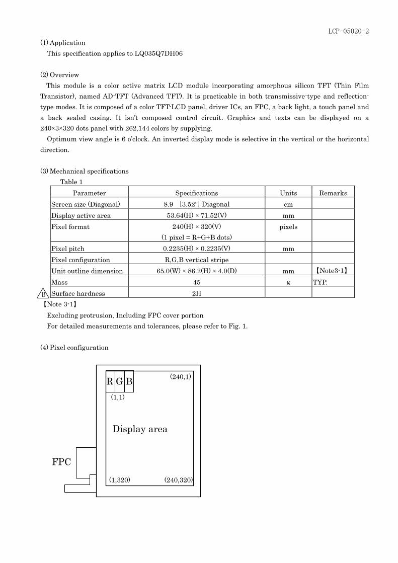
(1) Application This specification applies to LQ035Q7DH06 (2) Overview
This module is a color active matrix LCD module incorporating amorphous silicon TFT (Thin Film Transistor), named AD-TFT (Advanced TFT). It is practicable in both transmissive-type and reflection-type modes. It is composed of a color TFT-LCD panel, driver ICs, an FPC, a back light, a touch panel and a back sealed casing. It isn’t composed control circuit. Graphics and texts can be displayed on a 240×3×320 dots panel with 262,144 colors by supplying. Optimum view angle is 6 o’clock. An inverted display mode is selective in the vertical or the horizontal direction. (3) Mechanical specifications Table 1
Parameter Specifications Units Remarks Screen size (Diagonal) 8.9 [3.52"] Diagonal cm Display active area 53.64(H) × 71.52(V) mm Pixel format 240(H) × 320(V)
(1 pixel = R+G+B dots) pixels
Pixel pitch 0.2235(H) × 0.2235(V) mm Pixel configuration R,G,B vertical stripe Unit outline dimension 65.0(W) × 86.2(H) × 4.0(D) mm 【Note3-1】Mass 45 g TYP. Surface hardness 2H
【Note 3-1】 Excluding protrusion, Including FPC cover portion For detailed measurements and tolerances, please refer to Fig. 1.
(4) Pixel configuration
(1,320) (240,320)
(240,1)
(1,1)
R G B
Display area
FPC
B
LCP-05020-3
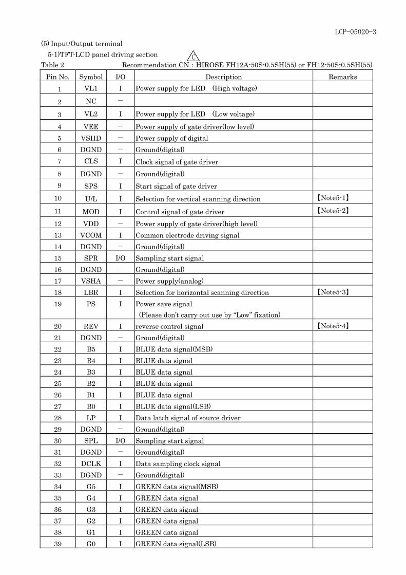
(5) Input/Output terminal 5-1)TFT-LCD panel driving section
Table 2 Recommendation CN:HIROSE FH12A-50S-0.5SH(55) or FH12-50S-0.5SH(55) Pin No. Symbol I/O Description Remarks
1 VL1 I Power supply for LED (High voltage)
2 NC -
3 VL2 I Power supply for LED (Low voltage)
4 VEE - Power supply of gate driver(low level) 5 VSHD - Power supply of digital 6 DGND - Ground(digital) 7 CLS I Clock signal of gate driver
8 DGND - Ground(digital) 9 SPS I Start signal of gate driver
10 U/L I Selection for vertical scanning direction 【Note5-1】
11 MOD I Control signal of gate driver 【Note5-2】
12 VDD - Power supply of gate driver(high level) 13 VCOM I Common electrode driving signal 14 DGND - Ground(digital) 15 SPR I/O Sampling start signal 16 DGND - Ground(digital) 17 VSHA - Power supply(analog) 18 LBR I Selection for horizontal scanning direction 【Note5-3】 19 PS I Power save signal
(Please don’t carry out use by “Low” fixation)
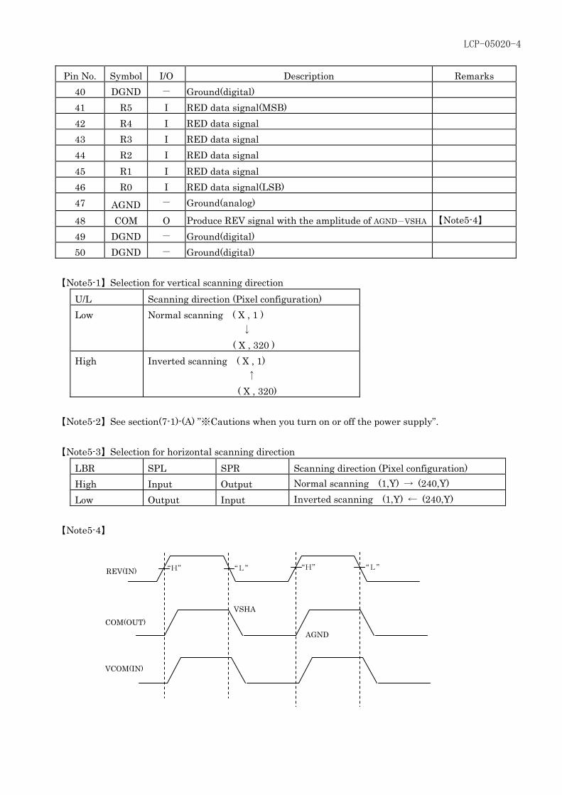
20 REV I reverse control signal 【Note5-4】 21 DGND - Ground(digital) 22 B5 I BLUE data signal(MSB) 23 B4 I BLUE data signal 24 B3 I BLUE data signal 25 B2 I BLUE data signal 26 B1 I BLUE data signal 27 B0 I BLUE data signal(LSB) 28 LP I Data latch signal of source driver 29 DGND - Ground(digital) 30 SPL I/O Sampling start signal 31 DGND - Ground(digital) 32 DCLK I Data sampling clock signal 33 DGND - Ground(digital) 34 G5 I GREEN data signal(MSB) 35 G4 I GREEN data signal 36 G3 I GREEN data signal 37 G2 I GREEN data signal 38 G1 I GREEN data signal 39 G0 I GREEN data signal(LSB)
C
LCP-05020-4
Pin No. Symbol I/O Description Remarks
40 DGND - Ground(digital) 41 R5 I RED data signal(MSB) 42 R4 I RED data signal 43 R3 I RED data signal 44 R2 I RED data signal 45 R1 I RED data signal 46 R0 I RED data signal(LSB) 47 AGND - Ground(analog)
48 COM O Produce REV signal with the amplitude of AGND-VSHA 【Note5-4】 49 DGND - Ground(digital) 50 DGND - Ground(digital)
【Note5-1】Selection for vertical scanning direction
U/L Scanning direction (Pixel configuration) Low Normal scanning ( X , 1 )
↓ ( X , 320 )
High Inverted scanning ( X , 1) ↑ ( X , 320)
【Note5-2】See section(7-1)-(A) ”※Cautions when you turn on or off the power supply”. 【Note5-3】Selection for horizontal scanning direction
LBR SPL SPR Scanning direction (Pixel configuration) High Input Output Normal scanning (1,Y) → (240,Y) Low Output Input Inverted scanning (1,Y) ← (240,Y)
【Note5-4】
“H” “L” “H” “L”REV(IN)
COM(OUT) VSHA
AGND
VCOM(IN)
LCP-05020-5
5-2) Touch panel driving section
Table 3 Recommendation CN:0.4(1.0)9FLH-SM1-GB-TB(JST) Pin No. Symbol I/O Description Remark
T1 YU - Y (12 o’clock side) T2 XL - X (right side) T3 YD - Y (6 o’clock side) T4 XR - X (left side)
(6) Absolute Maximum Ratings
Table 4 Parameter Symbol Condition Ratings Unit Remark Power supply(source/Analog) VSHA Ta=25℃ -0.3~+7.0 V Power supply(source/Digital) VSHD Ta=25℃ -0.3~+7.0 V Power supply (gate) VDD Ta=25℃ -0.3~+35.0 V Power supply (gate) VDD-VEE Ta=25℃ -0.3~+35.0 V Input voltage (Digital) VID Ta=25℃ -0.3~VSHD+0.3 V [Terminal①] Operating temperature (panel surface)
Topp - -10~70 ℃ 【Note6-1】
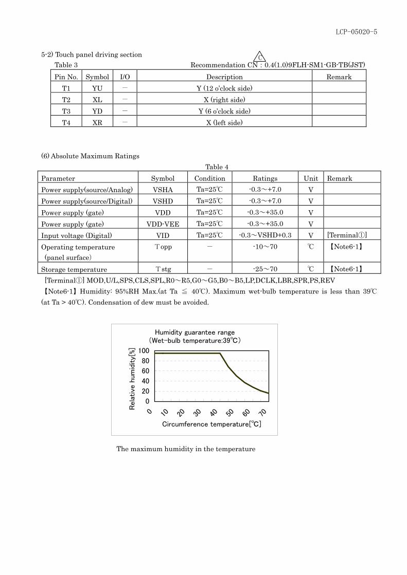
Storage temperature Tstg - -25~70 ℃ 【Note6-1】 [Terminal①] MOD,U/L,SPS,CLS,SPL,R0~R5,G0~G5,B0~B5,LP,DCLK,LBR,SPR,PS,REV 【Note6-1】Humidity: 95%RH Max.(at Ta ≦ 40℃). Maximum wet-bulb temperature is less than 39℃ (at Ta > 40℃). Condensation of dew must be avoided.
Humidity guarantee range(Wet-bulb temperature:39℃)
0
20
40
60
80
100
0 10 20 30 40 50 60 70
Circumference temperature[℃]
Rela
tive
hum
idity[
%]
The maximum humidity in the temperature
C
LCP-05020-6
(7) Electrical characteristics 7-1)Recommended operating conditions A) TFT-LCD panel driving section Table 5 GND=0V
Parameter Symbol Min. Typ. Max. Unit Remarks Supply voltage for source driver (Analog)
VSHA +4.5 +5.0 +5.5 V
Supply voltage for source driver (Digital)
VSHD +3.0 +3.3 +3.6 V
Supply voltage for gate driver
High voltage VDD +14.5 +15.0 +15.5 V
Low voltage VEE -10.5 -10.0 -9.5 V Input voltage for Source driver (Low) VILS GND - 0.2VSHD V 【Note 7-1】 Input voltage for Source driver (High) VIHS 0.8VSHD - VSHD V 【Note 7-1】 Input current for Source driver (Low) IILS - - 30 μA 【Note 7-1】
IIHS1 - - 30 μA 【Note 7-2】 Input current for Source driver (High)
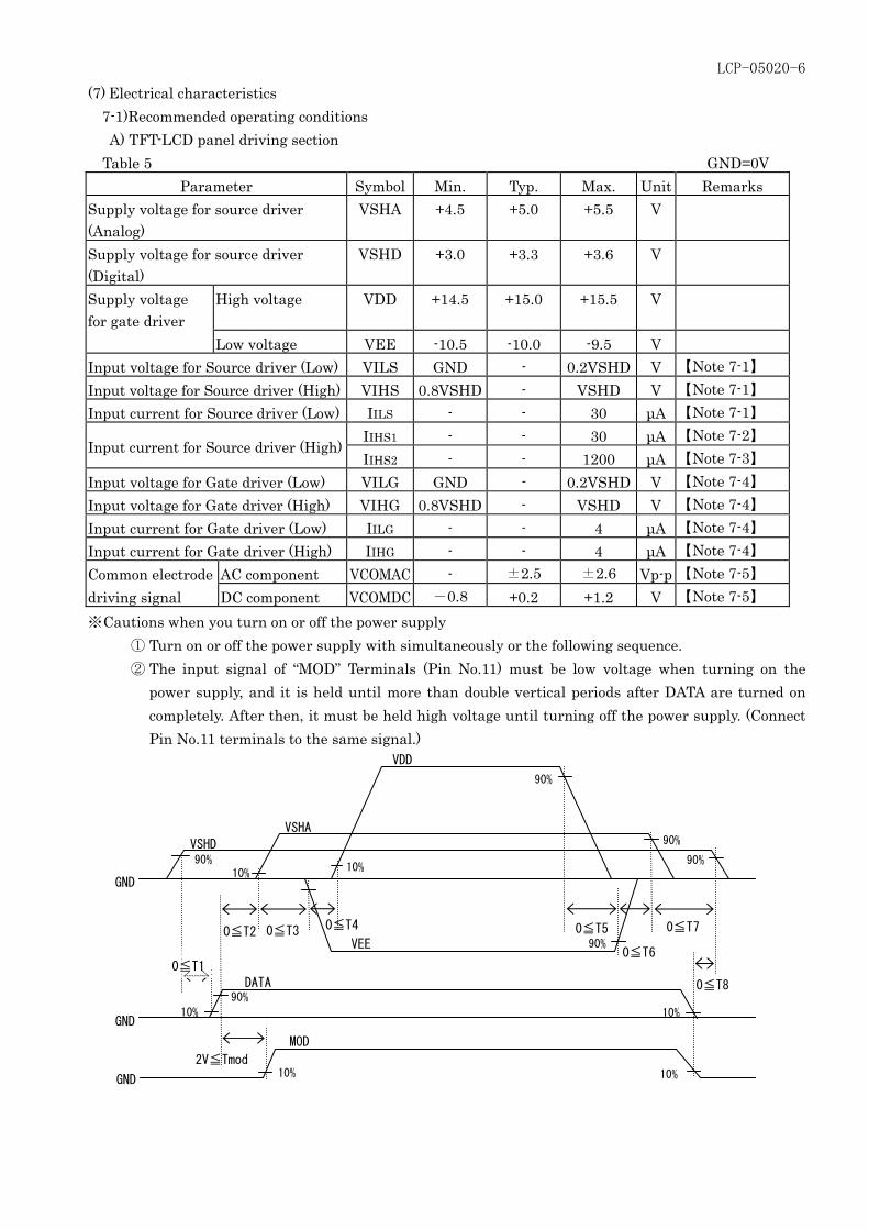
IIHS2 - - 1200 μA 【Note 7-3】 Input voltage for Gate driver (Low) VILG GND - 0.2VSHD V 【Note 7-4】 Input voltage for Gate driver (High) VIHG 0.8VSHD - VSHD V 【Note 7-4】 Input current for Gate driver (Low) IILG - - 4 μA 【Note 7-4】 Input current for Gate driver (High) IIHG - - 4 μA 【Note 7-4】 Common electrode AC component VCOMAC - ±2.5 ±2.6 Vp-p 【Note 7-5】 driving signal DC component VCOMDC -0.8 +0.2 +1.2 V 【Note 7-5】 ※ Cautions when you turn on or off the power supply
① Turn on or off the power supply with simultaneously or the following sequence. ② The input signal of “MOD” Terminals (Pin No.11) must be low voltage when turning on the
power supply, and it is held until more than double vertical periods after DATA are turned on completely. After then, it must be held high voltage until turning off the power supply. (Connect Pin No.11 terminals to the same signal.)
DATA
GND
MOD
VEE
VSHD
VSHA
VDD
GND
GND
0≦T1
0≦T2 0≦T3 0≦T4 0≦T5
0≦T6
0≦T7
0≦T8
2V≦Tmod
10% 90%
90%
10%
10%
90%
10%
10%
90%
90%
90%
10%
LCP-05020-7
【Note 7-1】DCLK,SPL,SPR,LBR,LP,PS,REV,R0~R5,G0~G5 and B0~B5 terminals are applied. 【Note 7-2】DCLK,SPL,SPR,LBR,LP,REV,R0~R5,G0~G5 and B0~B5 terminals are applied. 【Note 7-3】PS terminal is applied. 【Note 7-4】MOD,CLS,SPS and U/L terminals are applied. 【Note 7-5】VCOMAC should be alternated on VCOMDC every 1 horizontal period and 1 vertical period. VCOMDC bias is adjusted so as to minimize flicker or maximum contrast every each module.
B) Back light driving section Table 6 Ta=25℃
Parameter Symbol MIN TYP MAX Units Remarks terminal LED voltage VL - 19.2 21.6 V LED current IL - 20 22 mA Power consumption WL - 0.384 - W 【Note 7-6】 【Note 7-6】Calculated reference value(IL×VL)
LCP-05020-8
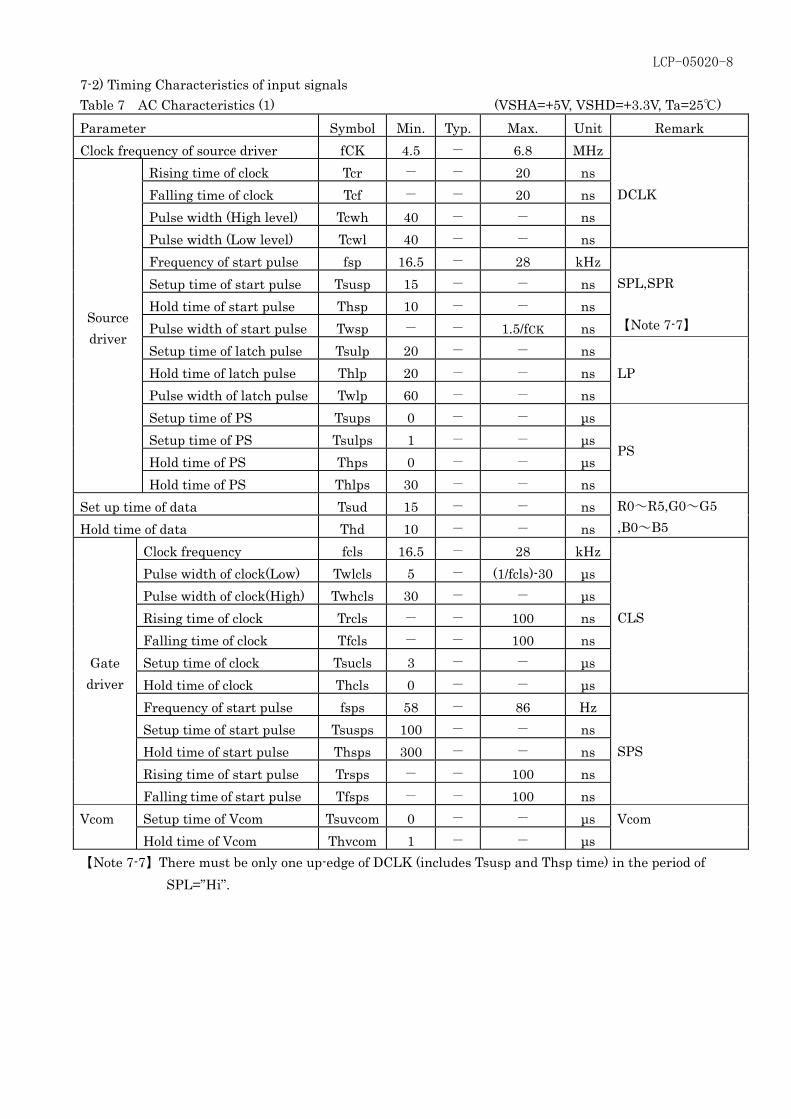
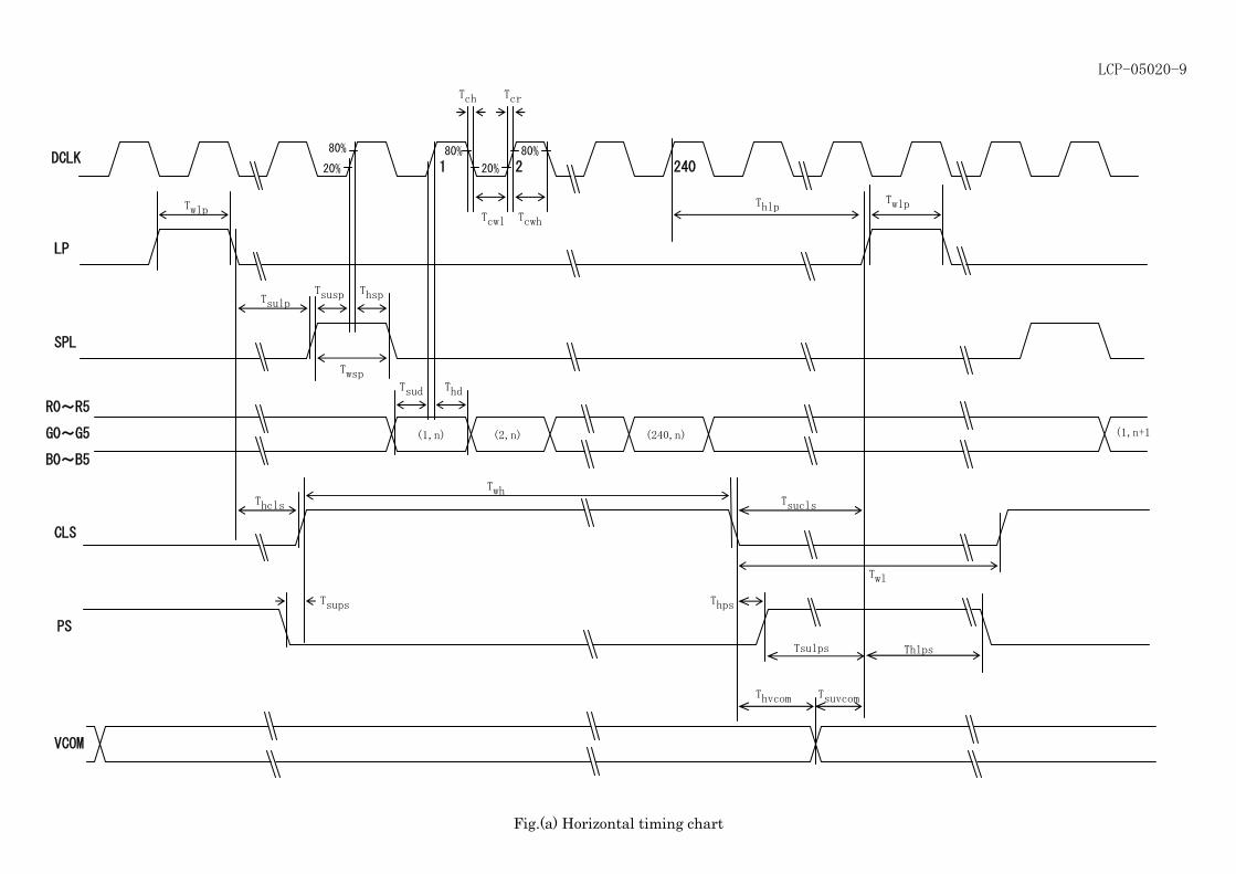
7-2) Timing Characteristics of input signals Table 7 AC Characteristics (1) (VSHA=+5V, VSHD=+3.3V, Ta=25℃) Parameter Symbol Min. Typ. Max. Unit Remark Clock frequency of source driver fCK 4.5 - 6.8 MHz
Rising time of clock Tcr - - 20 ns Falling time of clock Tcf - - 20 ns Pulse width (High level) Tcwh 40 - - ns Pulse width (Low level) Tcwl 40 - - ns
DCLK
Frequency of start pulse fsp 16.5 - 28 kHz Setup time of start pulse Tsusp 15 - - ns Hold time of start pulse Thsp 10 - - ns Pulse width of start pulse Twsp - - 1.5/fCK ns
SPL,SPR 【Note 7-7】
Setup time of latch pulse Tsulp 20 - - ns Hold time of latch pulse Thlp 20 - - ns LP Pulse width of latch pulse Twlp 60 - - ns Setup time of PS Tsups 0 - - μs Setup time of PS Tsulps 1 - - μs Hold time of PS Thps 0 - - μs
Source driver
Hold time of PS Thlps 30 - - ns
PS
Set up time of data Tsud 15 - - ns Hold time of data Thd 10 - - ns
R0~R5,G0~G5 ,B0~B5
Clock frequency fcls 16.5 - 28 kHz Pulse width of clock(Low) Twlcls 5 - (1/fcls)-30 μs Pulse width of clock(High) Twhcls 30 - - μs Rising time of clock Trcls - - 100 ns Falling time of clock Tfcls - - 100 ns Setup time of clock Tsucls 3 - - μs Hold time of clock Thcls 0 - - μs
CLS
Frequency of start pulse fsps 58 - 86 Hz Setup time of start pulse Tsusps 100 - - ns Hold time of start pulse Thsps 300 - - ns Rising time of start pulse Trsps - - 100 ns
Gate driver
Falling time of start pulse Tfsps - - 100 ns
SPS
Vcom Setup time of Vcom Tsuvcom 0 - - μs Vcom Hold time of Vcom Thvcom 1 - - μs 【Note 7-7】There must be only one up-edge of DCLK (includes Tsusp and Thsp time) in the period of SPL=”Hi”.
LCP-05020-9
Fig.(a) Horizontal timing chart
Twlp
Tsusp Thsp
(1,n) (2,n) (240,n) (1,n+1
Twlp Thlp
Tsulp
Tsud Thd
Tcwl Tcwh
Tch Tcr
80%
20%
80%
20%
80%
2 240
Twsp
Twh
Twl
DCLK
LP
SPL
R0~R5
G0~G5
B0~B5
CLS
PS
VCOM
Thcls Tsucls
Tsups Thps
Tsuvcom Thvcom
1
Tsulps Thlps
LCP-05020-10
Fig.(b) Vertical timing chart
1
Tsusps
80%CLS
SPS
2 8 9 327
Thsps
Trcls Tfcls
Trsps Tfsps
20% 20%
20%
80% 80%
20%
20%
(1~240,1) (1~240,2) (1~240,320)
1 2
fcls
1
Twlcls
Twhcls
20%
80%
LINE1 LINE2 LINE320
fsps 1
R0~R5
G0~G5
B0~B5
Non-display period Non-display period
LCP-05020-11
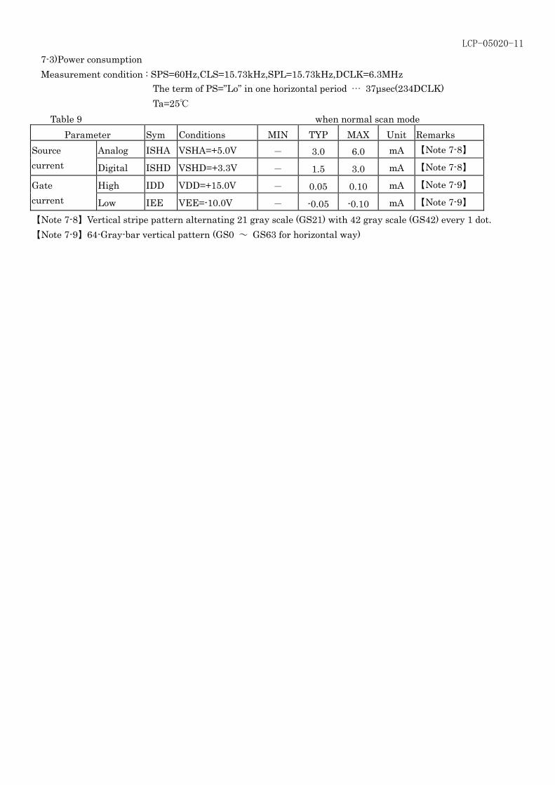
7-3)Power consumption Measurement condition : SPS=60Hz,CLS=15.73kHz,SPL=15.73kHz,DCLK=6.3MHz The term of PS=”Lo” in one horizontal period … 37μsec(234DCLK) Ta=25℃
Table 9 when normal scan mode Parameter Sym Conditions MIN TYP MAX Unit Remarks
Analog ISHA VSHA=+5.0V - 3.0 6.0 mA 【Note 7-8】 Source current Digital ISHD VSHD=+3.3V - 1.5 3.0 mA 【Note 7-8】
High IDD VDD=+15.0V - 0.05 0.10 mA 【Note 7-9】 Gate current Low IEE VEE=-10.0V - -0.05 -0.10 mA 【Note 7-9】
【Note 7-8】Vertical stripe pattern alternating 21 gray scale (GS21) with 42 gray scale (GS42) every 1 dot. 【Note 7-9】64-Gray-bar vertical pattern (GS0 ~ GS63 for horizontal way)
LCP-05020-12
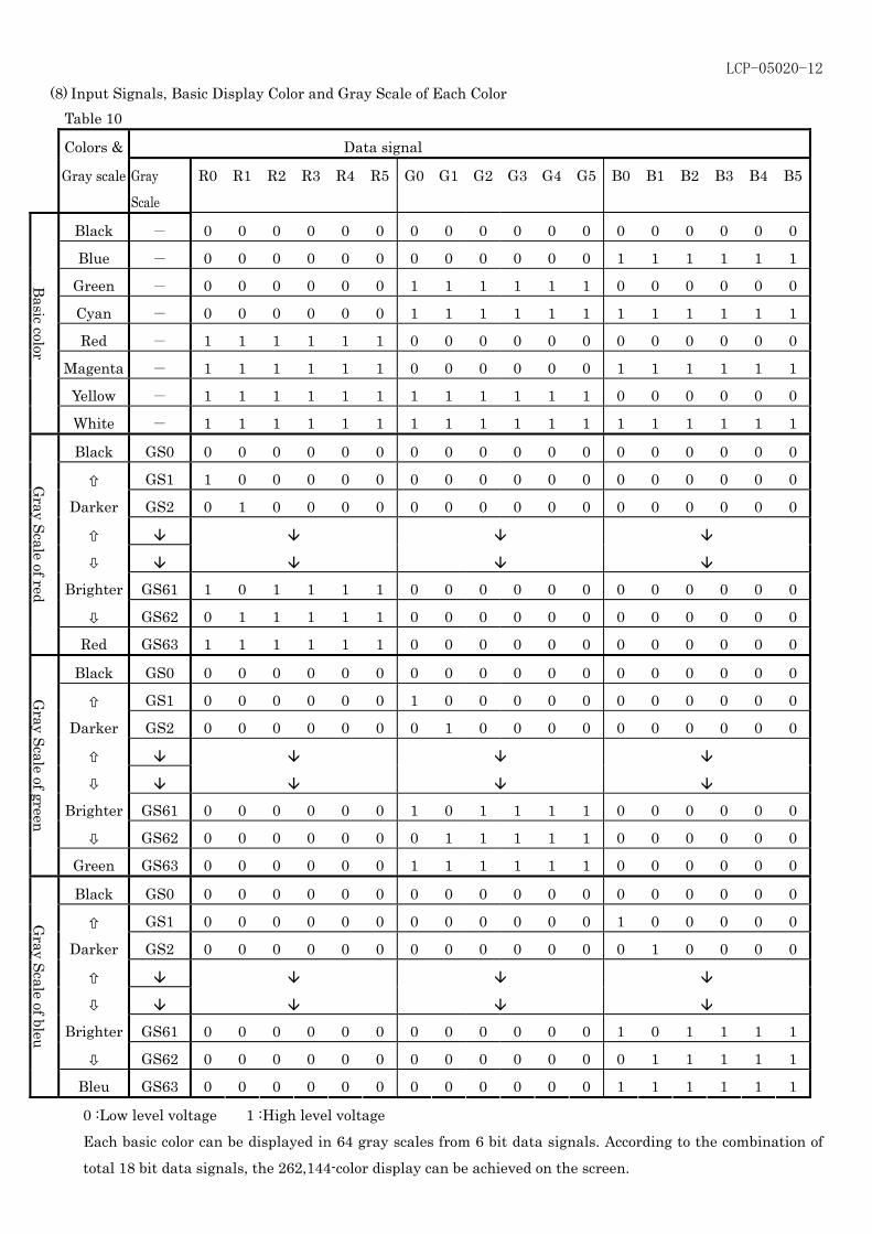
(8) Input Signals, Basic Display Color and Gray Scale of Each Color Table 10
Colors & Data signal
Gray scale Gray
Scale
R0 R1 R2 R3 R4 R5 G0 G1 G2 G3 G4 G5 B0 B1 B2 B3 B4 B5
Black - 0 0 0 0 0 0 0 0 0 0 0 0 0 0 0 0 0 0
Blue - 0 0 0 0 0 0 0 0 0 0 0 0 1 1 1 1 1 1
Green - 0 0 0 0 0 0 1 1 1 1 1 1 0 0 0 0 0 0
Cyan - 0 0 0 0 0 0 1 1 1 1 1 1 1 1 1 1 1 1
Red - 1 1 1 1 1 1 0 0 0 0 0 0 0 0 0 0 0 0
Magenta - 1 1 1 1 1 1 0 0 0 0 0 0 1 1 1 1 1 1
Yellow - 1 1 1 1 1 1 1 1 1 1 1 1 0 0 0 0 0 0
Basic color
White - 1 1 1 1 1 1 1 1 1 1 1 1 1 1 1 1 1 1
Black GS0 0 0 0 0 0 0 0 0 0 0 0 0 0 0 0 0 0 0
GS1 1 0 0 0 0 0 0 0 0 0 0 0 0 0 0 0 0 0
Darker GS2 0 1 0 0 0 0 0 0 0 0 0 0 0 0 0 0 0 0
Brighter GS61 1 0 1 1 1 1 0 0 0 0 0 0 0 0 0 0 0 0
GS62 0 1 1 1 1 1 0 0 0 0 0 0 0 0 0 0 0 0
Gray Scale of red
Red GS63 1 1 1 1 1 1 0 0 0 0 0 0 0 0 0 0 0 0
Black GS0 0 0 0 0 0 0 0 0 0 0 0 0 0 0 0 0 0 0
GS1 0 0 0 0 0 0 1 0 0 0 0 0 0 0 0 0 0 0
Darker GS2 0 0 0 0 0 0 0 1 0 0 0 0 0 0 0 0 0 0
Brighter GS61 0 0 0 0 0 0 1 0 1 1 1 1 0 0 0 0 0 0
GS62 0 0 0 0 0 0 0 1 1 1 1 1 0 0 0 0 0 0 G
ray Scale of green
Green GS63 0 0 0 0 0 0 1 1 1 1 1 1 0 0 0 0 0 0
Black GS0 0 0 0 0 0 0 0 0 0 0 0 0 0 0 0 0 0 0
GS1 0 0 0 0 0 0 0 0 0 0 0 0 1 0 0 0 0 0
Darker GS2 0 0 0 0 0 0 0 0 0 0 0 0 0 1 0 0 0 0
Brighter GS61 0 0 0 0 0 0 0 0 0 0 0 0 1 0 1 1 1 1
GS62 0 0 0 0 0 0 0 0 0 0 0 0 0 1 1 1 1 1
Gray Scale of bleu
Bleu GS63 0 0 0 0 0 0 0 0 0 0 0 0 1 1 1 1 1 1
0 :Low level voltage 1 :High level voltage
Each basic color can be displayed in 64 gray scales from 6 bit data signals. According to the combination of
total 18 bit data signals, the 262,144-color display can be achieved on the screen.
LCP-05020-13
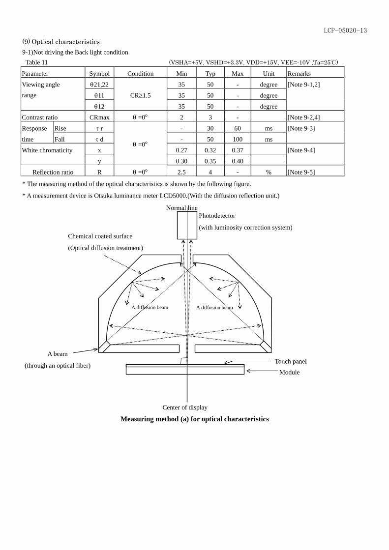
(9) Optical characteristics 9-1)Not driving the Back light condition Table 11 (VSHA=+5V, VSHD=+3.3V, VDD=+15V, VEE=-10V ,Ta=25℃)
Parameter Symbol Condition Min Typ Max Unit Remarks
θ21,22 35 50 - degree [Note 9-1,2]
θ11 CR≥1.5 35 50 - degree
Viewing angle range
θ12 35 50 - degree
Contrast ratio CRmax θ =0° 2 3 - [Note 9-2,4]
Response Rise τ r - 30 60 ms [Note 9-3]
time Fall τ d - 50 100 ms
White chromaticity x 0.27 0.32 0.37 [Note 9-4]
y
θ =0°
0.30 0.35 0.40
Reflection ratio R θ =0° 2.5 4 - % [Note 9-5]
* The measuring method of the optical characteristics is shown by the following figure.
* A measurement device is Otsuka luminance meter LCD5000.(With the diffusion reflection unit.) Center of display
Measuring method (a) for optical characteristics
Photodetector (with luminosity correction system)
Module
Chemical coated surface
(Optical diffusion treatment)
A diffusion beam A diffusion beam
Normal line
A beam
(through an optical fiber) Touch panel
LCP-05020-14
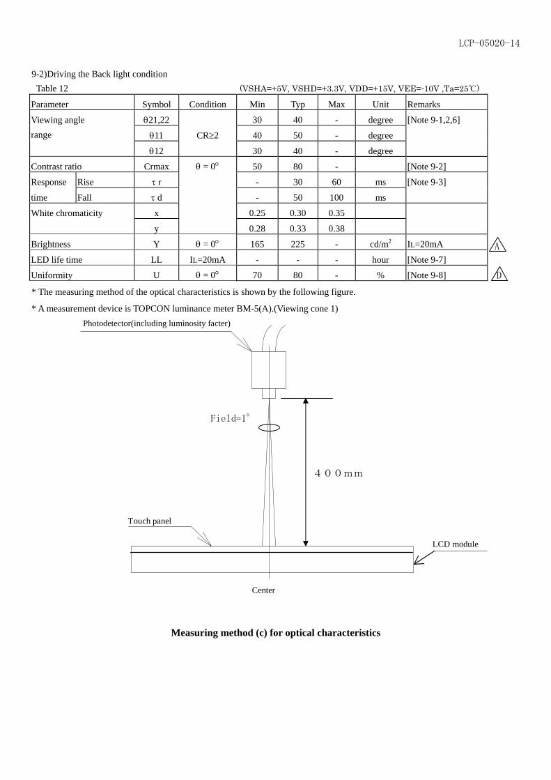
9-2)Driving the Back light condition Table 12 (VSHA=+5V, VSHD=+3.3V, VDD=+15V, VEE=-10V ,Ta=25℃)
Parameter Symbol Condition Min Typ Max Unit Remarks
θ21,22 30 40 - degree [Note 9-1,2,6]
θ11 CR≥2 40 50 - degree
Viewing angle range
θ12 30 40 - degree
Contrast ratio Crmax θ = 0° 50 80 - [Note 9-2]
Response Rise τ r - 30 60 ms [Note 9-3]
time Fall τ d - 50 100 ms
White chromaticity x 0.25 0.30 0.35
y
0.28 0.33 0.38
Brightness Y θ = 0° 165 225 - cd/m2 IL=20mA
LED life time LL IL=20mA - - - hour [Note 9-7]
Uniformity U θ = 0° 70 80 - % [Note 9-8]
* The measuring method of the optical characteristics is shown by the following figure.
* A measurement device is TOPCON luminance meter BM-5(A).(Viewing cone 1)
Measuring method (c) for optical characteristics
Photodetector(including luminosity facter)
Center
Touch panel
LCD module
A
400mm
Field=1°
D
LCP-05020-15
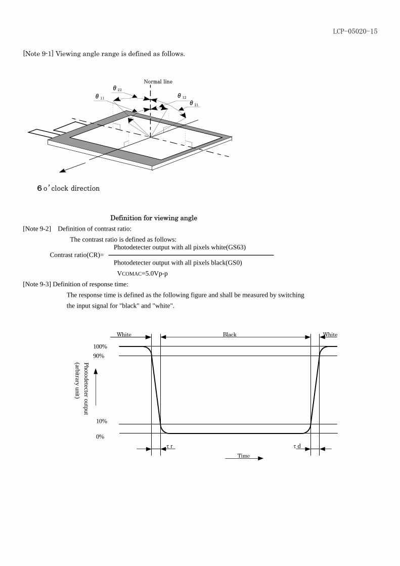
[Note 9-1] Viewing angle range is defined as follows.
6o’clock direction
θ12
θ22
θ11 θ21
Normal line
Definition for viewing angle [Note 9-2] Definition of contrast ratio: The contrast ratio is defined as follows: Photodetecter output with all pixels white(GS63) Contrast ratio(CR)= Photodetecter output with all pixels black(GS0) VCOMAC=5.0Vp-p [Note 9-3] Definition of response time: The response time is defined as the following figure and shall be measured by switching the input signal for "black" and "white".
0%
10%
90%100%
Black WhiteWhite
τ d τ rTime
Photodetecter output(arbitrary unit)
LCP-05020-16
[Note 9-4] A measurement device is Minolta CM-2002. [Note 9-5] Definition of reflection ratio Reflection ratio = [Note 9-6] A measurement device is ELDIM EZContrast [Note 9-7] This is the reference value. The White-LED life time is defind as a time when brightness not to become
under 50% of the original value(at Ta=25℃)
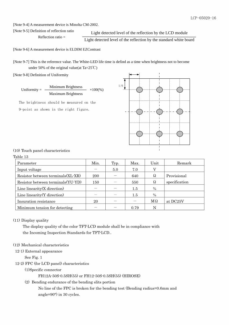
[Note 9-8] Definition of Uniformity
The brightness should be measured on the
9-point as shown in the right figure.
(10) Touch panel characteristics Table 13
Parameter Min. Typ. Max. Unit Remark Input voltage - 5.0 7.0 V Resistor between terminals(XL-XR) 200 - 640 Ω Resistor between terminals(YU-YD) 150 - 550 Ω
Provisional specification
Line linearity(X direction) - - 1.5 % Line linearity(Y direction) - - 1.5 % Insuration resistance 20 - - MΩ at DC25V Minimum tension for detecting - - 0.79 N
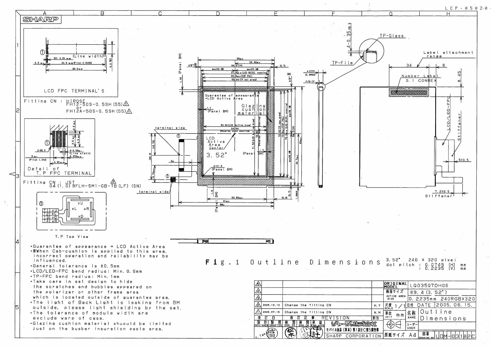
(11) Display quality The display quality of the color TFT-LCD module shall be in compliance with the Incoming Inspection Standards for TFT-LCD.. (12) Mechanical characteristics 12-1) External appearance
See Fig. 1 12-2) FPC (for LCD panel) characteristics
(1)Specific connector FH12A-50S-0.5SH(55) or FH12-50S-0.5SH(55) (HIROSE)
(2) Bending endurance of the bending slits portion No line of the FPC is broken for the bending test (Bending radius=0.6mm and angle=90°) in 30 cycles.
Light detected level of the reflection by the LCD module Light detected level of the reflection by the standard white board
Minimum Brightness
Maximum Brightness Uniformity = ×100(%)
1/6
LCP-05020-17
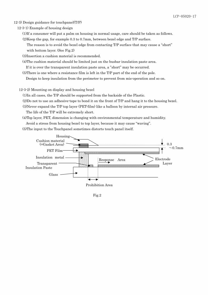
12-3) Design guidance for touchpanel(T/P) 12-3-1) Example of housing design (1)If a consumer will put a palm on housing in normal usage, care should be taken as follows.
(2)Keep the gap, for example 0.3 to 0.7mm, between bezel edge and T/P surface. The reason is to avoid the bezel edge from contacting T/P surface that may cause a “short” with bottom layer. (See Fig.2)
(3)Insertion a cushion material is recommended. (4)The cushion material should be limited just on the busbar insulation paste area. If it is over the transparent insulation paste area, a ”short” may be occurred. (5)There is one where a resistance film is left in the T/P part of the end of the pole. Design to keep insulation from the perimeter to prevent from mis-operation and so on.
12-3-2) Mounting on display and housing bezel
(1)In all cases, the T/P should be supported from the backside of the Plastic. (2)Do not to use an adhesive-tape to bond it on the front of T/P and hang it to the housing bezel. (3)Never expand the T/P top layer (PET-film) like a balloon by internal air pressure.
The life of the T/P will be extremely short. (4)Top layer, PET, dimension is changing with environmental temperature and humidity. Avoid a stress from housing bezel to top layer, because it may cause “waving”. (5)The input to the Touchpanel sometimes distorts touch panel itself.
Fig.2
Housing Cushion material
PET Film
Insulation metal
Glass
Transparent Insulation Paste
Response Area
Prohibition Area
Electrode Layer
0.3 ~0.7mm
(=Gasket Area)
LCP-05020-18
(13) Handling Precautions 13-1) Insertion and taking out of FPCs Be sure insert and take out of the FPC into the connector of the set after turning off the power supply on the set side. 13-2) Handling of FPCs The FPC for LCD panel shall be bent only slit portion. The bending slit shall be bent uniformly on the whole slit portion with bending radius larger than 0.6mm ,and only inner side (back side of the module). Don’t bend it outer side (display surface side). Don’t give the FPCs too large force, for example, hanging the module with holding FPC. 13-3) Installation of the module
On mounting the module, be sure to fix the module on the same plane. Taking care not to warp or twist the module.
13-4) Precautions when mounting (1) If water droplets and oil attaches to it for a long time, discoloration and staining occurs. Wipe them off
immediately. (2) Glass is used for the TFT-LCD panel. If it is dropped or bumped against a hard object, it may be broken.
Handle it with sufficient care. (3) As the CMOS IC is used in this module, pay attention to static electricity when handling it. Take a
measure for grounding on the human body. 13-5) Others
(1) The liquid-crystal is deteriorated by ultraviolet rays. Do not leave it in direct sunlight and strong ultraviolet rays for many hours.
(2) If it is kept at a temperature below the rated storage temperature, it becomes coagulated and the panel may be broken. Also, if it is kept at a temperature above the rated storage temperature, it becomes isotropic liquid and does not return to its original state. Therefore, it is desirable to keep it at room temperature as much as possible.
(3) If the LCD breaks, don’t put internal liquid crystal into the mouth. When the liquid crystal sticks to the hands, feet and clothes, wash it out immediately.
(4) Wipe off water drop or finger grease immediately. Long contact with water may cause discoloration or spots.
(5) Observe general precautions for all electronic components. (6) VCOM must be adjusted on condition of your final product. No adjustment causes the deterioration for
display quality. (7) Static image should not be displayed more than 5 minutes in order to prevent from occurrence of
residual image. (8) If local pressure joins T/P surface for a long time, it will become the cause of generating of Newton’s ring.
LCP-05020-19
(14) Reliability Test Conditions for TFT-LCD Module Table 14
No. Test items Test conditions 1 High temperature storage test Ta=+70℃ 240h
2 Low temperature storage test Ta=-25℃ 240h
3 High temperature and high
humidity operating test Tp=+40℃ , 95%RH 240h (But no condensation of dew)
4 High temperature operating test Tp=+70℃ 240h 5 Low temperature operating test Tp=-10℃ 240h 6 Electro static discharge test ±200V・200pF(0Ω) to Terminals(Contact)
(1 time for each terminals) ±8kV・150pF(330Ω) to Housing bezel or TP(Contact) ±15kV・150pF(330Ω) to Housing bezel or TP(in Air)
7 Shock tset 980 m/s2, 6 ms ±X,±Y,±Z 3 times for each direction (JIS C0041, A-7 Condition C)
8 Vibration test Frequency range: 10Hz~55Hz Stroke: 1.5 mm Sweep: 10Hz~55Hz X,Y,Z 2 hours for each direction (total 6 hours) (JIS C0040,A-10 Condition A)
9 Heat shock test Ta=-25℃~+70℃ / 5 cycles (1h) (1h)
10 Point activation test (Touch panel)
Hit it 1,000,000 times with a silicon rubber of R8 HS 60. Hitting force :2.4N Hitting speed : 3 times per second
11 Writing friction resistance test (Touch panel)
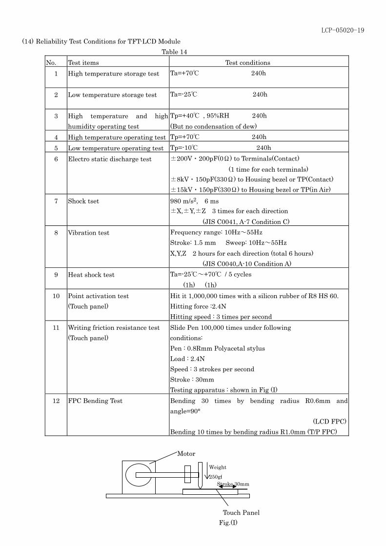
Slide Pen 100,000 times under following conditions: Pen : 0.8Rmm Polyacetal stylus Load : 2.4N Speed : 3 strokes per second Stroke : 30mm Testing apparatus : shown in Fig (I)
12 FPC Bending Test
Bending 30 times by bending radius R0.6mm and angle=90°
(LCD FPC) Bending 10 times by bending radius R1.0mm (T/P FPC)
Motor
Touch Panel
Stroke 30mm
Weight
250gf
Fig.(I)
LCP-05020-20
【Note】Ta = Ambient temperature, Tp = Panel temperature 【Check items】
(a)Test No.1~9 In the standard condition, there shall be no practical problems that may affect the display function. (b)Test No.10~No.11
The measurements after the tests are satisfied (10)-Table 13 (Touch panel characteristics) (15) Others 15-1) Indication of lot number
The lot number is shown on a label. Attached location is shown in Fig.1 (Outline Dimensions). Indicated contents of the label LQ035Q7DH06 ○○○○○○○○★ model No. lot No. T/P Code (E:j-TOUCH, G:Gunze, Y:Young Fast) 15-2) Used Regulation of Chemical Substances Breaking Ozone Stratum Substances with the object of regulating: CFCS, Carbon tetrachloride, Halon 1,1,1-Trichloro ethane (Methyl chloroform)
(a) This LCD module, Constructed part and Parts don’t contain the above substances. (b) This LCD module, Constructed part and Parts don’t contain the above substances in processes of
manufacture.
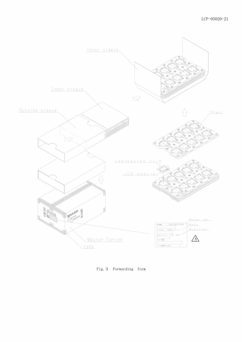
15-3) If some problems arise about mentioned items in this document and other items, the user of the TFT-LCD module and Sharp will cooperate and make efforts to solve the problems with mutual respect and good will. (16) Forwarding form(see Fig.3 Package Form) (17) Piling number of cartons: Max 8 (18) Package quantity in one cartons: 100pcs (19) Carton size: 575mm × 332mm × 209mm (20) Total mass of 1 carton filled with full modules: 8000g
Conditions for storage. Environment (1)Temperature : 0~40℃ (2)Humidity : 60%RH or less (at 40℃) No dew condensation at low temperature and high humidity. (3)Atmosphere : Harmful gas, such as acid or alkali which bites electronic components and/or wires, must not be detected. (4)Period : about 3 months (5)Opening of the package : In order to prevent the LCD module from breakdown by electrostatic charges, please control the room humidity over 50%RH and open the package taking sufficient countermeasures against electrostatic charges, such as earth, etc.
A
LCP-05020-21
Fig.3 Forwarding form
A
LCP-05020-22
Fig.1 Outline Dimensions
AvnET EmBEddEd officES.
LocAL AvnET EmBEddEd BuSinESSES:
06/2010
www.avnet-embedded.eu
All trademarks and logos are the property of their respective owners. This document provides a brief overview only and is not intended to be complete or binding offer. Product information, including information related to a product‘s specifications, uses or conformance with legal or other requirements, is obtained by Avnet from its suppliers or other sources deemed reliable and is provided by Avnet on an „As Is“ basis. Avnet makes no representation as to the accuracy or completeness of the product information and Avnet disclaims all representations, warranties and liabilities under any theory with respect to the product information, including any implied warranties of merchantability, fitness for a particular purpose, title and/or non-refringement. All product information is subject to change without notice.
dEnmArkAvnet EmbeddedAvnet Nortec A/SEllekær 92730 HerlevPhone: +45 3678 6250Fax: +45 3678 [email protected]
finLAndAvnet EmbeddedAvnet Nortec OyTiilenpolttajankuja 3 A B1720 VantaaPhone: +358 207 499260Fax: +358 942 [email protected]
frAncEAvnet EmbeddedAvnet EMG France SAImmeuble 154, Parc Chene 25, allée du General Benoist69000 BronPhone: +33 4 72 81 02 30Fax: +33 4 72 81 02 [email protected]
Avnet EmbeddedAvnet EMG France SA4, rue de la CoutureBâtiment Milan, BP 20209 94518 Rungis Cedex Phone: +33 1 49 78 88 88 Fax: +33 1 49 78 88 89 [email protected]
Avnet EmbeddedAvnet EMG France SAZA la Hallerais le Semiramis2, allée du Communel35770 Vern sur SeichePhone: +33 2 99 77 37 02Fax: +33 2 99 77 33 [email protected]
GErmAnY (AuSTriA, cZEcH rEpuBLic, HunGArY, poLAnd, SWiTZErLAnd)Avnet EmbeddedAvnet EMG GmbHGruber Straße 60c85586 PoingPhone: +49 8121 775 500 Fax: +49 8121 775 [email protected]
Avnet EmbeddedAvnet EMG GmbHLötscher Weg 6641334 NettetalPhone: +49 8121 775 500Fax: +49 8121 775 [email protected]
iTALY (porTuGAL, SpAin)Avnet EmbeddedAvnet EMG Italy SRLVia Manzoni, 4420095 Cusano MilaninoPhone: +39 02 66092 1Fax: +39 02 66092 [email protected]
nETHErLAndS (BELGium, LuXEmBourG)Avnet EmbeddedAvnet B.V.Takkebijsters 24802 BL BredaPhone: +31 76 5722400Fax: +31 76 [email protected]
SWEdEn (norWAY)Avnet EmbeddedAvnet Nortec ABEsplanaden 3 D172 67 SundbybergPhone: +46 8 564 725 50Fax: +46 8 760 01 [email protected]
uniTEd kinGdom (irELAnd)Avnet EmbeddedAvnet EMG Ltd.Pilgrims Court, 15/17 West StreetReigate, Surrey, RH2 9BLPhone: +44 1737 227800Fax: +44 1737 [email protected]


![Lecture 4 BJT Small Signal Analysis01 [??????????????????]pws.npru.ac.th/thawatchait/data/files/Lecture 4 BJT Small... · 2016-09-12 · Lecture 4 BJJg yT Small Signal Analysis Present](https://img.pdfslide.tips/doc/110x75/5e674360ee8da93175055e37/lecture-4-bjt-small-signal-analysis01-pwsnpruacththawatchaitdatafileslecture.jpg)