Embed Size (px)
Citation preview

8/7/2019 B156RW01 V.0
http://slidepdf.com/reader/full/b156rw01-v0 1/37
1 of 37
AU OPTRONICS CORPORATION
Product Specification
B156RW01 V0 Document Version : 0.1
B156RW01 V0
( V ) Preliminary Specifications
( ) Final Specifications
Module 15.6” HD+(15.55) Color TFT-LCD with LED Backlight design
Model Name B156RW01 V0 (H/W:1A)
Note ( ) LED Backlight with driving circuit design
Customer Date
Checked &Approved by
Date
Note: This Specification is subject to changewithout notice.
Approved by Date
Prepared by
NBBU Marketing Division /
AU Optronics corporation

8/7/2019 B156RW01 V.0
http://slidepdf.com/reader/full/b156rw01-v0 2/37
2 of 37
AU OPTRONICS CORPORATION
Product Specification
B156RW01 V0 Document Version : 0.1
Contents1. Handling Precautions .......................................................................................... 4
2. General Description ............................................................................................. 5
2.1 General Specification .........................................................................................................5
2.2 Optical Characteristics.......................................................................................................6
3. Functional Block Diagram................................................................................. 11
4. Absolute Maximum Ratings .............................................................................. 12
4.1 Absolute Ratings of TFT LCD Module..............................................................................12
4.2 Absolute Ratings of Environment .....................................................................................12
5. Electrical characteristics................................................................................... 13
5.1 TFT LCD Module..............................................................................................................13
5.2 Backlight Unit ...................................................................................................................15
6. Signal Characteristic.......................................................................................... 16
6.1 Pixel Format Image ..........................................................................................................16
6.2 The input data format .......................................................................................................17
6.3 Integration Interface and Pin Assignment ........................................................................18
6.4 Interface Timing................................................................................................................22
7. Connector Description....................................................................................... 25
7.1 TFT LCD Module..............................................................................................................258. LED Driving Specification ................................................................................. 26
8.1 Connector Description......................................................................................................26
8.2 Pin Assignment.................................................................................................................26
9. Vibration and Shock Test .................................................................................. 27
9.1 Vibration Test ...................................................................................................................27
9.2 Shock Test Spec:..............................................................................................................27
10. Reliability........................................................................................................... 28
11. Mechanical Characteristics............................................................................. 29 11.1 LCM Outline Dimension..................................................................................................29
11.2 Screw Hole Depth and Center Position..........................................................................31
12. Shipping and Package..................................................................................... 32
12.1 Shipping Label Format...................................................................................................32
12.2 Carton package..............................................................................................................33
12.3 Shipping package of palletizing sequence.....................................................................33
13. Appendix: EDID description............................................................................ 34

8/7/2019 B156RW01 V.0
http://slidepdf.com/reader/full/b156rw01-v0 3/37
3 of 37
AU OPTRONICS CORPORATION
Product Specification
B156RW01 V0 Document Version : 0.1
Record of Revision
Version and Date Page Old description New Description Remark
0.1 2009/01/13 All First Edition for Customer

8/7/2019 B156RW01 V.0
http://slidepdf.com/reader/full/b156rw01-v0 4/37
4 of 37
AU OPTRONICS CORPORATION
Product Specification
B156RW01 V0 Document Version : 0.1
1. Handling Precautions
1) Since front polarizer is easily damaged, pay attention not to scratch it.
2) Be sure to turn off power supply when inserting or disconnecting from input connector.
3) Wipe off water drop immediately. Long contact with water may cause discoloration or
spots.
4) When the panel surface is soiled, wipe it with absorbent cotton or other soft cloth.
5) Since the panel is made of glass, it may break or crack if dropped or bumped on hard
surface.
6) Since CMOS LSI is used in this module, take care of static electricity and insure human
earth when handling.
7) Do not open nor modify the Module Assembly.8) Do not press the reflector sheet at the back of the module to any directions.
9) At the insertion or removal of the Signal Interface Connector, be sure not to rotate nor
tilt the Interface Connector of the TFT Module.
11)After installation of the TFT Module into an enclosure (Notebook PC Bezel, for
example), do not twist nor bend the TFT Module even momentary. At designing the
enclosure, it should be taken into consideration that no bending/twisting forces are
applied to the TFT Module from outside. Otherwise the TFT Module may be damaged.
12) Small amount of materials having no flammability grade is used in the LCD module. The LCD
module should be supplied by power complied with requirements of Limited Power Source
(IEC60950 or UL1950), or be applied exemption.
13) Disconnecting power supply before handling LCD modules, it can prevent electric shock, DO
NOT TOUCH the electrode parts, cables, connectors and LED circuit part of TFT module that
a LED light bar build in as a light source of back light unit. It can prevent electrostic
breakdown.

8/7/2019 B156RW01 V.0
http://slidepdf.com/reader/full/b156rw01-v0 5/37
5 of 37
AU OPTRONICS CORPORATION
Product Specification
B156RW01 V0 Document Version : 0.1
2. General Description
B156RW01 V0 is a Color Active Matrix Liquid Crystal Display composed of a TFT LCD panel, a
driver circuit, and LED backlight system. The screen format is intended to support the HD+(1600(H) x 900(V)) screen and 262k colors (RGB 6-bits data driver) with LED backlight driving
circuit. All input signals are LVDS interface compatible.
B156RW01 V0 is designed for a display unit of notebook style personal computer and industrialmachine.
2.1 General Specification
The following items are characteristics summary on the table at 25℃ condition:
Items Unit SpecificationsScreen Diagonal [mm] 394.87 15.6”(15.55)
Active Area [mm] 344.16 X 193.59
Pixels H x V 1600x3(RGB) x 900
Pixel Pitch [mm] 0.215X0.215
Pixel Format R.G.B. Vertical Stripe
Display Mode Normally White
White Luminance (ILED=20mA) (Note: ILED is LED current)
[cd/m2] 250 typ. (5 points average)
215 min. (5 points average)
Luminance Uniformity 1.25 max. (5 points)1.53 max. (13 points)
Contrast Ratio 400:1
Response Time [ms] 8 typ/12max
Nominal Input Voltage VDD [Volt] +3.3 typ.
Power Consumption(Include Logic andBLU power)
[Watt] 7.5 max. @ 250nits2.4 max. @ 60nits
Weight [Grams] 460 max.
Min. Typ. Max.
Length - - 359.8
Width - - 210
Physical Size without inverter,bracket.
[mm]
Thickness - - 5.7
Electrical Interface 2 channel LVDS
Glass Thickness [mm] 0.5
Surface Treatment Glare, Hardness 3H,Reflection <=5%
Support Color 262K colors ( RGB 6-bit )
Temperature RangeOperatingStorage (Non-Operating)
[oC]
[oC]
0 to +50-20 to +60
RoHS Compliance RoHS Compliance

8/7/2019 B156RW01 V.0
http://slidepdf.com/reader/full/b156rw01-v0 6/37
6 of 37
AU OPTRONICS CORPORATION
Product Specification
B156RW01 V0 Document Version : 0.1
2.2 Optical Characteristics
The optical characteristics are measured under stable conditions at 25℃ (Room Temperature) :
Item Symbol Conditions Min. Typ. Max. Unit Note
White Luminance
ILED=20mA
5 points average215 250 - cd/m
2 1, 4, 5.
θR
θL
Horizontal (Right)
CR = 10 (Left)
-
-
70
70
-
-
degre
e Viewing Angle
ψH
ψL
Vertical (Upper)
CR = 10 (Lower)
-
-
60
60
-
-
4, 9
Luminance
Uniformityδ5P 5 Points - - 1.25 1, 3, 4
Luminance
Uniformityδ13P 13 Points - - 1.53 2, 3, 4
Contrast Ratio CR - 400 - 4, 6
Cross talk % TBD 4, 7
Tr Rising - TBD -
Tf Falling - TBD -Response Time
TRT Rising + Falling - 8 12
msec 4, 8
Rx - TBD -
Red Ry - TBD -
Gx - TBD -Green
Gy - TBD -
Bx - TBD -Blue
By - TBD -
Wx 0.283 0.313 0.343
Color /
Chromaticity
Coodinates
WhiteWy 0.299 0.329 0.359
NTSC %
CIE 1931
- 60 -
4

8/7/2019 B156RW01 V.0
http://slidepdf.com/reader/full/b156rw01-v0 7/37
7 of 37
AU OPTRONICS CORPORATION
Product Specification
B156RW01 V0 Document Version : 0.1
Note 1: 5 points position (Ref: Active area)
1 2
3
4 5
H /4
H /4
H /4
H /4
H
W
W /4 W /4 W /4 W /4
Note 2: 13 points position (Ref: Active area)
W /4
W
W /4
H
H /4
H /4
H /4
H /4
7
9 10
W /4
1
8
W /4
10
1 0
10
1 0
2 3
1312
4 5
6
1 1
Note 3: The luminance uniformity of 5 or13 points is defined by dividing the maximum luminance values by theminimum test point luminance
Note 4: Measurement method
The LCD module should be stabilized at given temperature for 30 minutes to avoid abrupt temperature change
during measuring. In order to stabilize the luminance, the measurement should be executed after lighting Backlight
δW13 = Maximum Brightness of thirteen points
Minimum Brightness of thirteen points
Maximum Brightness of five pointsδW5 =
Minimum Brightness of five points

8/7/2019 B156RW01 V.0
http://slidepdf.com/reader/full/b156rw01-v0 8/37
8 of 37
AU OPTRONICS CORPORATION
Product Specification
B156RW01 V0 Document Version : 0.1
for 30 minutes in a stable, windless and dark room, and it should be measured in the center of screen.
Note 5 Definition of Average Luminance of White (YL):
Measure the luminance of gray level 63 at 5 pointsYL = [L (1)+ L (2)+ L (3)+ L (4)+ L (5)] / 5
L (x) is corresponding to the luminance of the point X at Figure in Note (1).
Note 6 Definition of contrast ratio:
Contrast ratio is calculated with the following formula.
Note 7 Definition of Cross Talk (CT)
CT = | YB – YA | / YA × 100 (%)
Where
YA = Luminance of measured location without gray level 0 pattern (cd/m2)
YB = Luminance of measured location with gray level 0 pattern (cd/m2)
Center of the screen
TFT-LCD
50 cm
Photo detector
LCD Panel
Field=2°
Contrast ratio (CR)= Bri htness on the “White” state
Bri htness on the “Black” state
8/7/2019 B156RW01 V.0
http://slidepdf.com/reader/full/b156rw01-v0 9/37
9 of 37
AU OPTRONICS CORPORATION
Product Specification
B156RW01 V0 Document Version : 0.1
Note 8: Definition of response time:
The output signals of BM-7 or equivalent are measured when the input signals are changed from “Black” to“White” (falling time) and from “White” to “Black” (rising time), respectively. The response time interval between the
10% and 90% of amplitudes. Refer to figure as below.
Signal(Relativevalue)
"Black"
Tr Tf
"White""White"
0%10%
90%100%

8/7/2019 B156RW01 V.0
http://slidepdf.com/reader/full/b156rw01-v0 10/37
10 of 37
AU OPTRONICS CORPORATION
Product Specification
B156RW01 V0 Document Version : 0.1
Note 9. Definition of viewing angle
Viewing angle is the measurement of contrast ratio ≧ 10, at the screen center, over a 180° horizontal an d 180°
vertical range (off-normal v iewing angles). The 180° viewing angle range is broken down as follows; 90 ° ( θ)
horizontal left and right and 90° (Φ) vertical, high (up) and low (down). The measurement direction is typically
perpendicular to the display surface with the screen rotated about its center to develop the desired measurement
viewing angle.

8/7/2019 B156RW01 V.0
http://slidepdf.com/reader/full/b156rw01-v0 11/37
11 of 37
AU OPTRONICS CORPORATION
Product Specification
B156RW01 V0 Document Version : 0.1
3. Functional Block DiagramThe following diagram shows the functional block of the 15.6 inches wide Color TFT/LCD 40 Pin (OneCH/connector Module)

8/7/2019 B156RW01 V.0
http://slidepdf.com/reader/full/b156rw01-v0 12/37
12 of 37
AU OPTRONICS CORPORATION
Product Specification
B156RW01 V0 Document Version : 0.1
4. Absolute Maximum Ratings
An absolute maximum rating of the module is as following:
4.1 Absolute Ratings of TFT LCD Module
Item Symbol Min Max Unit ConditionsLogic/LCD Drive Vin -0.3 +4.0 [Volt] Note 1,2
4.2 Absolute Ratings of EnvironmentItem Symbol Min Max Unit Conditions
Operating Temperature TOP 0 +50 [oC] Note 4
Operation Humidity HOP 5 95 [%RH] Note 4
Storage Temperature TST -20 +60 [oC] Note 4
Storage Humidity HST 5 95 [%RH] Note 4
Note 1: At Ta (25℃ )
Note 2: Permanent damage to the device may occur if exceed maximum values
Note 3: LED specification refer to section 5.2
Note 4: For quality performance, please refer to AUO IIS (Incoming Inspection Standard).
Twb=39°C
Operating Range Storage Range
8/7/2019 B156RW01 V.0
http://slidepdf.com/reader/full/b156rw01-v0 13/37
13 of 37
AU OPTRONICS CORPORATION
Product Specification
B156RW01 V0 Document Version : 0.1
5. Electrical characteristics
5.1 TFT LCD Module
5.1.1 Power Specification
Input power specifications are as follows;
The power specification are measured under 25℃ and frame frenquency under 60Hz
Symble Parameter Min Typ Max Units Note
VDD Logic/LCD DriveVolta e
3.0 3.3 3.6 [Volt]
PDD VDD Power - - TBD [Watt] Note 1/2
IDD IDD Current - - TBD [mA] Note 1/2
IRush Inrush Current - - TBD [mA] Note 3VDDrp Allowable
Logic/LCD DriveRipple Voltage
- - TBD [mV]p-p
Note 1 : Maximum Measurement ConditionBlack Pattern
Note 2Typical Measurement Condition: Mosaic Pattern
Note 3Measure Condition
+5.0V
+12.0V
VCC
R147K
R2
1K
VR1
47K
SW1
SW MAG-SPST
1
2
F1
Q3AO6402
G
D2
S
D1
D5D6
C11uF/16V
Q3
AO6402
G
D2 SD1
D5D6
C3
0.01uF/25V
C21uF/25V
(High to Low)
Control
Signal
(LCD Module Input)
90%
10%
Vin rising time
0V
3.3V
0.5ms

8/7/2019 B156RW01 V.0
http://slidepdf.com/reader/full/b156rw01-v0 14/37
14 of 37
AU OPTRONICS CORPORATION
Product Specification
B156RW01 V0 Document Version : 0.1
5.1.2 Signal Electrical CharacteristicsInput signals shall be low or High-impedance state when VDD is off.
It is recommended to refer the specifications of THC63LVDF84A (Thine Electronics Inc.) indetail.
Signal electrical characteristics are as follows;
Parameter Condition Min Max Unit
VthDifferential Input HighThreshold (Vcm=+1.2V)
-100 [mV]
VtlDifferential Input LowThreshold (Vcm=+1.2V) -100
-[mV]
VcmDifferential Input
Common Mode Voltage1.125 1.375 [V]
Note: LVDS Signal Waveform
Vt
Vcm
VSS

8/7/2019 B156RW01 V.0
http://slidepdf.com/reader/full/b156rw01-v0 15/37
15 of 37
AU OPTRONICS CORPORATION
Product Specification
B156RW01 V0 Document Version: 0.1
5.2 Backlight Unit
LED Parameter guideline for LED driving selection (Ref. Remark 1)
Parameter Symbol Min Typ Max Units Condition
LED Forward Voltage VF 3.0 3.2 3.4 [Volt] (Ta=25℃)
LED Forward Current IF 20 30 [mA] (Ta=25℃)
LED Power
consumption
PLED 5.5 [Watt] (Ta=25℃)
Note 1 LED Life-Time N/A 10,000 - - Hour (Ta=25℃)
IF=20 mA
Note 2
Output PWM frequency F PWM 100 200 20K Hz
Duty ratio -- 5 -- 100 %
Note 1: Calculator value for reference IF×VF =P
Note 2: The LED life-time define as the estimated time to 50% degradation of initial luminous.
8/7/2019 B156RW01 V.0
http://slidepdf.com/reader/full/b156rw01-v0 16/37
16 of 37
AU OPTRONICS CORPORATION
Product Specification
B156RW01 V0 Document Version: 0.1
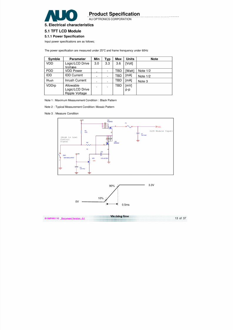
6. Signal Characteristic
6.1 Pixel Format Image
Following figure shows the relationship of the input signals and LCD pixel format.
R G B R G B
R G B R G B
R G B R G B
R G B R G B
1 1600 1st Line
900th Line

8/7/2019 B156RW01 V.0
http://slidepdf.com/reader/full/b156rw01-v0 17/37
17 of 37
AU OPTRONICS CORPORATION
Product Specification
B156RW01 V0 Document Version: 0.1
6.2 The input data format
Signal Name Description
R5
R4R3R2R1R0
Red Data 5 (MSB)
Red Data 4Red Data 3Red Data 2Red Data 1Red Data 0 (LSB)
Red-pixel Data
Red-pixel Data
Each red pixel's brightness data consists of these 6 bits pixel data.
G5G4G3G2G1G0
Green Data 5 (MSB)Green Data 4Green Data 3Green Data 2Green Data 1Green Data 0 (LSB)
Green-pixel Data
Green-pixel DataEach green pixel's brightness data consists of these 6 bits pixel data.
B5B4B3B2B1B0
Blue Data 5 (MSB)Blue Data 4Blue Data 3Blue Data 2Blue Data 1Blue Data 0 (LSB)
Blue-pixel Data
Blue-pixel DataEach blue pixel's brightness data consists of these 6 bits pixel data.
RxCLKIN Data Clock The signal is used to strobe the pixel data and DE signals. All pixel datashall be valid at the falling edge when the DE signal is high.
DE Display Timing This signal is strobed at the falling edge ofRxCLKIN. W hen the signal is high, the pixel data shall be valid to bedisplayed.
VS Vertical Sync The signal is synchronized to RxCLKIN .
HS Horizontal Sync The signal is synchronized to RxCLKIN .
Note: Output signals from any system shall be low or High-impedance state when VDD is off.

8/7/2019 B156RW01 V.0
http://slidepdf.com/reader/full/b156rw01-v0 18/37

8/7/2019 B156RW01 V.0
http://slidepdf.com/reader/full/b156rw01-v0 19/37
19 of 37
AU OPTRONICS CORPORATION
Product Specification
B156RW01 V0 Document Version: 0.1
35 PWM System PWM Signal Input
36 LED_EN LED enable pin(+3.3V Input)
37 NC No Connection (Reserve)
38 VLED LED Power Supply 7V-21V
39 VLED LED Power Supply 7V-21V
40 VLED LED Power Supply 7V-21V

8/7/2019 B156RW01 V.0
http://slidepdf.com/reader/full/b156rw01-v0 20/37
20 of 37
AU OPTRONICS CORPORATION
Product Specification
B156RW01 V0 Document Version: 0.1
Note1: Start from right side
Note2: Input signals shall be low or High-impedance state when VDD is off.
40 1
GN D
N C
Connector
IPEX-20455-040E-12

8/7/2019 B156RW01 V.0
http://slidepdf.com/reader/full/b156rw01-v0 21/37
21 of 37
AU OPTRONICS CORPORATION
Product Specification
B156RW01 V0 Document Version: 0.1
internal circuit of LVDS inputs are as following.The module uses a 100ohm resistor between positive and negative data lines of each receiver input
R
R
R
R
LVDS Receiver
Signal Input
Pin No.
9 11
12
14
15 17
18
8
RxIN0+
RxIN0-
RxIN1+
RxIN1-
RxIN2+
RxIN2-
RxCLKIN+
RxCLKIN-
8/7/2019 B156RW01 V.0
http://slidepdf.com/reader/full/b156rw01-v0 22/37
22 of 37
AU OPTRONICS CORPORATION
Product Specification
B156RW01 V0 Document Version: 0.1
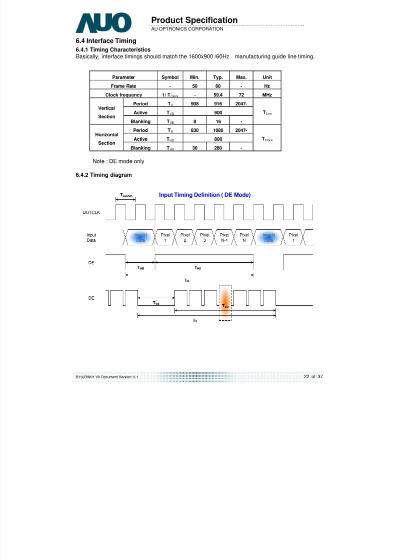
6.4 Interface Timing
6.4.1 Timing Characteristics
Basically, interface timings should match the 1600x900 /60Hz manufacturing guide line timing.
Parameter Symbol Min. Typ. Max. Unit
Frame Rate - 50 60 - Hz
Clock frequency 1/ TClock - 59.4 72 MHz
Period TV 908 916 2047-
Active TVD 900Vertical
SectionBlanking TVB 8 16 -
TLine
Period TH 830 1080 2047-
Active THD 800Horizontal
SectionBlanking THB 30 280 -
TClock
Note : DE mode only
6.4.2 Timing diagram
DOTCLK
DE
TH
THB THD
DE
TV
TVBTVD
Input Timing Definition ( DE Mode) TCLOCK
Input
Data
Pixel
1
Pixel
2
Pixel
3
Pixel
N-1
Pixel
N
Invaild
Data
Invaild
Data
Pixel
1

8/7/2019 B156RW01 V.0
http://slidepdf.com/reader/full/b156rw01-v0 23/37
23 of 37
AU OPTRONICS CORPORATION
Product Specification
B156RW01 V0 Document Version: 0.1
6.5 Power ON/OFF Sequence
VDD power on/off sequence is as follows. Interface signals are also shown in the chart. Signalsfrom any system shall be Hi-Z state or low level when VDD is off
Power Sequence Timing
Value
Parameter Min. Typ. Max. Units
T1 0.5 - 10
T2 0 - 50
T3 0 - 50
T4 400 - -
T5 200 - -
T6 200 - -
T7 0 - 10
ms

8/7/2019 B156RW01 V.0
http://slidepdf.com/reader/full/b156rw01-v0 24/37
24 of 37
AU OPTRONICS CORPORATION
Product Specification
B156RW01 V0 Document Version: 0.1
LED on/off sequence is as follows. Interface signals are also shown in the chart.
Values
Symbol Min Typ Max Unit
T1 10 --- ---
T2 10 --- ---
T3 50 --- ---
T4 0 --- ---
T5 10 --- ---
ms
Note: The duty of LED dimming signal should be more than 20% in T2 and T3.

8/7/2019 B156RW01 V.0
http://slidepdf.com/reader/full/b156rw01-v0 25/37
25 of 37
AU OPTRONICS CORPORATION
Product Specification
B156RW01 V0 Document Version: 0.1
7. Connector Description
Physical interface is described as for the connector on module.
These connectors are capable of accommodating the following signals and will be followingcomponents.
7.1 TFT LCD Module
Connector Name / Designation For Signal Connector
Manufacturer IPEX or compatible
Type / Part Number IPEX-20455-040E-12 or compatible
Mating Housing/Part Number IPEX-20453-040T-11 or compatible

8/7/2019 B156RW01 V.0
http://slidepdf.com/reader/full/b156rw01-v0 26/37
26 of 37
AU OPTRONICS CORPORATION
Product Specification
B156RW01 V0 Document Version: 0.1
8. LED Driving Specification
8.1 Connector Description
It is a intergrative interface and comibe into LVDS connector. The type and mating refer tosection 7.
8.2 Pin Assignment
Ref. to 6.3

8/7/2019 B156RW01 V.0
http://slidepdf.com/reader/full/b156rw01-v0 27/37
27 of 37
AU OPTRONICS CORPORATION
Product Specification
B156RW01 V0 Document Version: 0.1
9. Vibration and Shock Test
9.1 Vibration TestTest Spec:
Test method: Non-Operation
Acceleration: 1.5 G
Frequency: 10 - 500Hz Random
Sweep: 30 Minutes each Axis (X, Y, Z)
9.2 Shock Test Spec:
Test Spec:
Test method: Non-Operation
Acceleration: 220 G , Half sine wave
Active time: 2 ms
Pulse: X,Y,Z .one time for each side

8/7/2019 B156RW01 V.0
http://slidepdf.com/reader/full/b156rw01-v0 28/37
28 of 37
AU OPTRONICS CORPORATION
Product Specification
B156RW01 V0 Document Version: 0.1
10. Reliability
Items Required Condition Note
TemperatureHumidity Bias
Ta= 40℃℃℃℃, 90%RH, 300h
High Temperature
OperationTa= 50℃℃℃℃, Dry, 300h
Low Temperature
OperationTa= 0℃℃℃℃, 300h
High Temperature
StorageTa= 60℃℃℃℃, 35%RH, 300h
Low Temperature
StorageTa= -20℃℃℃℃, 50%RH, 250h
Thermal Shock
TestTa=-20℃℃℃℃to 60℃℃℃℃, Duration at 30 min, 100 cycles
ESDContact : ±8 KV
Air : ±15 KV
Note 1
Note1: According to EN 61000-4-2 , ESD class B: Some performance degradation allowed. No data lost
. Self-recoverable. No hardware failures.
Remark: MTBF (Excluding the LED): 30,000 hours with a confidence level 90%

8/7/2019 B156RW01 V.0
http://slidepdf.com/reader/full/b156rw01-v0 29/37
AU OPTRONICS CORPORATION
Product Specification
B156RW01 V0 Document Version: 0.1
11. Mechanical Characteristics
11.1 LCM Outline Dimension

8/7/2019 B156RW01 V.0
http://slidepdf.com/reader/full/b156rw01-v0 30/37
AU OPTRONICS CORPORATION
Product Specification
B156RW01 V0 Document Version: 0.1
Note: Prevention IC damage, IC positions not allowed any overlap over these

8/7/2019 B156RW01 V.0
http://slidepdf.com/reader/full/b156rw01-v0 31/37
31 of 37
AU OPTRONICS CORPORATION
Product Specification
B156RW01 V0 Document Version: 0.1
11.2 Screw Hole Depth and Center Position
Screw hole minimum depth, from side surface = 2.5 mm Max. (See drawing)
Screw hole center location, from front surface = 3.1±
0.3mm (See drawing)Screw Torque: Maximum 2.5 kgf-cm

8/7/2019 B156RW01 V.0
http://slidepdf.com/reader/full/b156rw01-v0 32/37
32 of 37
AU OPTRONICS CORPORATION
Product Specification
B156RW01 V0 Document Version: 0.1
12. Shipping and Package
12.1 Shipping Label Format
Week code Model name
H/W

8/7/2019 B156RW01 V.0
http://slidepdf.com/reader/full/b156rw01-v0 33/37
33 of 37
AU OPTRONICS CORPORATION
Product Specification
B156RW01 V0 Document Version: 0.1
12.2 Carton package(TBD)
12.3 Shipping package of palletizing sequence

8/7/2019 B156RW01 V.0
http://slidepdf.com/reader/full/b156rw01-v0 34/37
34 of 37
AU OPTRONICS CORPORATION
Product Specification
B156RW01 V0 Document Version: 0.1
13. Appendix: EDID description (TBD)
Address FUNCTION Value Value Value Note
HEX
0001
02
03
04
05
06
07
08
09
0A
0B
0C
0D
0E
0F
10
11
12
13
14
15
16
17
18
19
1A
1B
1C
1D
1E
1F
20
21
22
23
24
25
26

8/7/2019 B156RW01 V.0
http://slidepdf.com/reader/full/b156rw01-v0 35/37
35 of 37
AU OPTRONICS CORPORATION
Product Specification
B156RW01 V0 Document Version: 0.1
27
28
29
2A
2B
2C
2D
2E
2F
30
31
32
3334
35
36
37
38
39
3A
3B
3C
3D
3E
3F
40
41
42
43
44
45
46
47
48
49
4A
4B
4C
4D4E
4F
50
51

8/7/2019 B156RW01 V.0
http://slidepdf.com/reader/full/b156rw01-v0 36/37
36 of 37
AU OPTRONICS CORPORATION
Product Specification
B156RW01 V0 Document Version: 0.1
52
53
54
55
56
57
58
59
5A
5B
5C
5D
5E5F
60
61
62
63
64
65
66
67
68
69
6A
6B
6C
6D
6E
6F
70
71
72
73
74
75
76
77
7879
7A
7B
7C

8/7/2019 B156RW01 V.0
http://slidepdf.com/reader/full/b156rw01-v0 37/37
AU OPTRONICS CORPORATION
Product Specification
7D
7E
7F


![#2 & ) 0 # %%#$' % $2 - icamanzioranuccialfieri.it · ³,pshjqr h 5hvsrqvdelolwj shu xqd 6fxrod &rpxqlwj´ #!# \^ #!# \ ] \2 + v ) +v\0%+#$+ #2 & ) 0 # %%#$' % $2 '+, ] _\ \ v \ ]](https://img.pdfslide.tips/doc/110x75/6046025af5b6a4392651b5d7/2-0-2-ica-pshjqr-h-5hvsrqvdelolwj-shu-xqd-6fxrod-rpxqlwj.jpg)