Embed Size (px)
Citation preview
EE 330 Lecture 31
• Basic Amplifier Analysis • High-Gain Amplifiers • Current Source Biasing
– (just introduction)
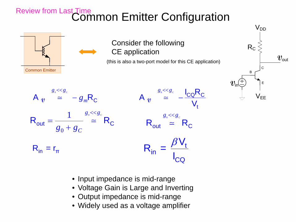
Common Emitter Configuration
Common Emitter
Consider the following CE application
B
E
C
VDD
Vin
RC
Vout
VEE0
CA RCg g
mg<<
−V
in πR = r
• Input impedance is mid-range • Voltage Gain is Large and Inverting • Output impedance is mid-range • Widely used as a voltage amplifier
0
0
1out CR R
Cg g
Cg g
<<
=+
0CQ C
t
I RA
VCg g<<
−V
0
out CR RCg g<<
tin
CQ
VR = Iβ
(this is also a two-port model for this CE application)
Review from Last Time
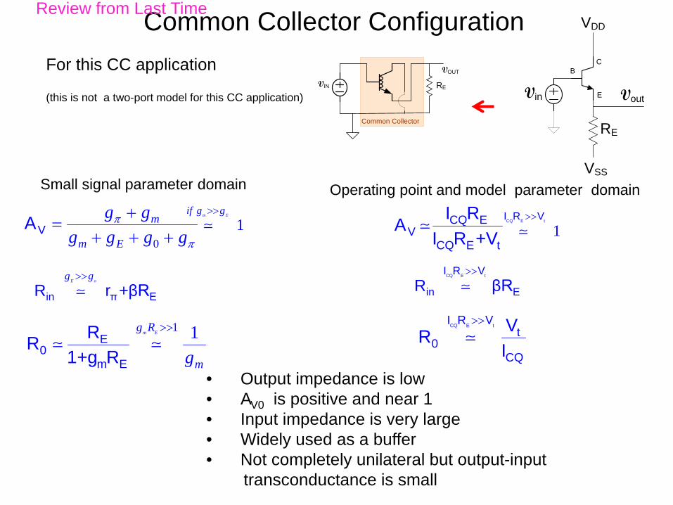
Common Collector Configuration For this CC application B
E
C
VSS
VDD
Vin
RE
Vout
0VA m
m E
g gg g g g
π
π
+=
+ + +
in π ER r +βRE og g>>
1 1E0
m E
RR1+g R
m Eg R
mg
>>
• Output impedance is low • AV0 is positive and near 1 • Input impedance is very large • Widely used as a buffer • Not completely unilateral but output-input transconductance is small
CQ EV
CQ E t
I RA
I R +V
CQ E tI R V
in ER βR>>
CQ E tI R Vt
0CQ
VRI
>>
(this is not a two-port model for this CC application)
1m Eif g g>>
1CQ E tI R V>>
Common Collector
REVIN
VOUT
Small signal parameter domain Operating point and model parameter domain
Review from Last Time
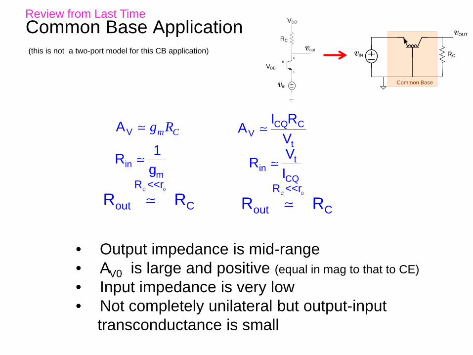
Common Base Application B
E
C
VBB
VDD
Vin
RC
Vout
C 0R <<r
out CR R
VA m Cg R
inm
1Rg
CQ CV
t
I RA
V
tin
CQ
VRI
C 0R <<r
out CR R
• Output impedance is mid-range • AV0 is large and positive (equal in mag to that to CE) • Input impedance is very low • Not completely unilateral but output-input transconductance is small
(this is not a two-port model for this CB application) VIN
Common Base
RC
VOUT
Review from Last Time
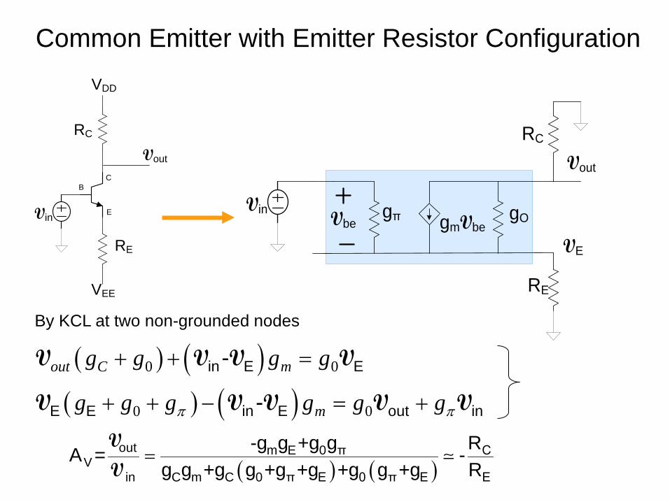
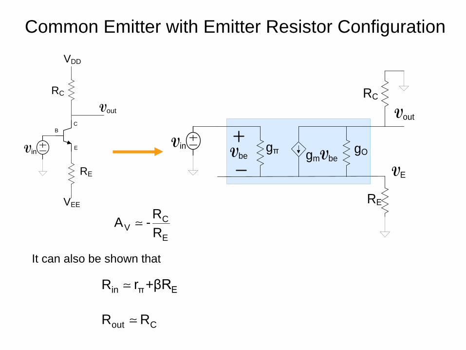
Common Emitter with Emitter Resistor Configuration
B
E
C
VDD
Vin
RC
Vout
RE
VEE
Vbe gOgmVbegπ
Vin
RC
RE
Vout
VE
By KCL at two non-grounded nodes
( ) ( )0 0in E E-out C mg g g g+ + =V V V V
( ) ( )0 0E E in E out in- mg g g g g gπ π+ + − = +V V V V V
( ) ( )out m E 0 π C
Vin C m C 0 π E 0 π E E
-g g +g g RA = -g g +g g +g +g +g g +g R
=
V
V
Common Emitter with Emitter Resistor Configuration
B
E
C
VDD
Vin
RC
Vout
RE
VEE
Vbe gOgmVbegπ
Vin
RC
RE
Vout
VE
CV
E
RA -R
It can also be shown that
out CR R
in π ER r +βR
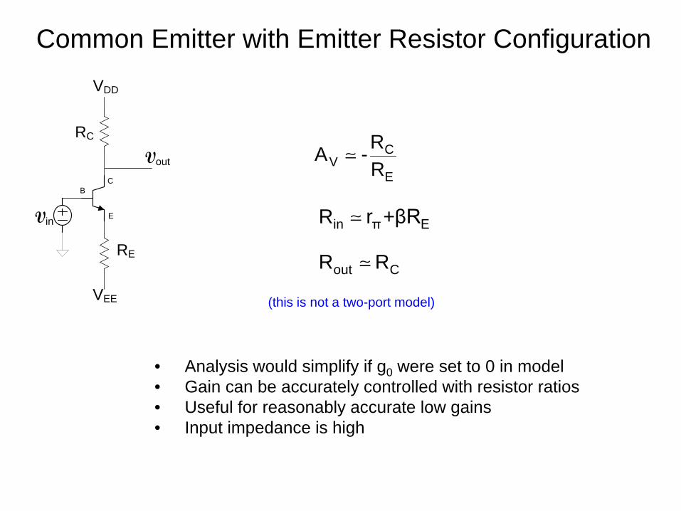
Common Emitter with Emitter Resistor Configuration
B
E
C
VDD
Vin
RC
Vout
RE
VEE
CV
E
RA -R
out CR R
in π ER r +βR
• Analysis would simplify if g0 were set to 0 in model • Gain can be accurately controlled with resistor ratios • Useful for reasonably accurate low gains • Input impedance is high
(this is not a two-port model)
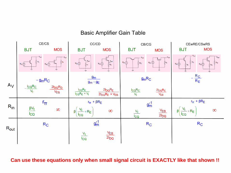
Can use these equations only when small signal circuit is EXACTLY like that shown !!
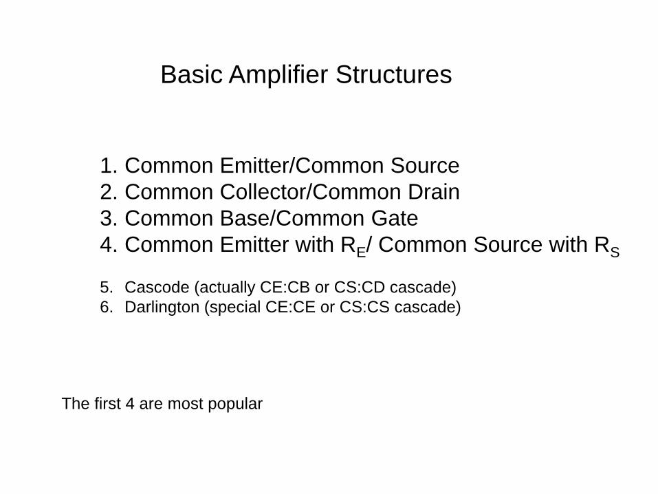
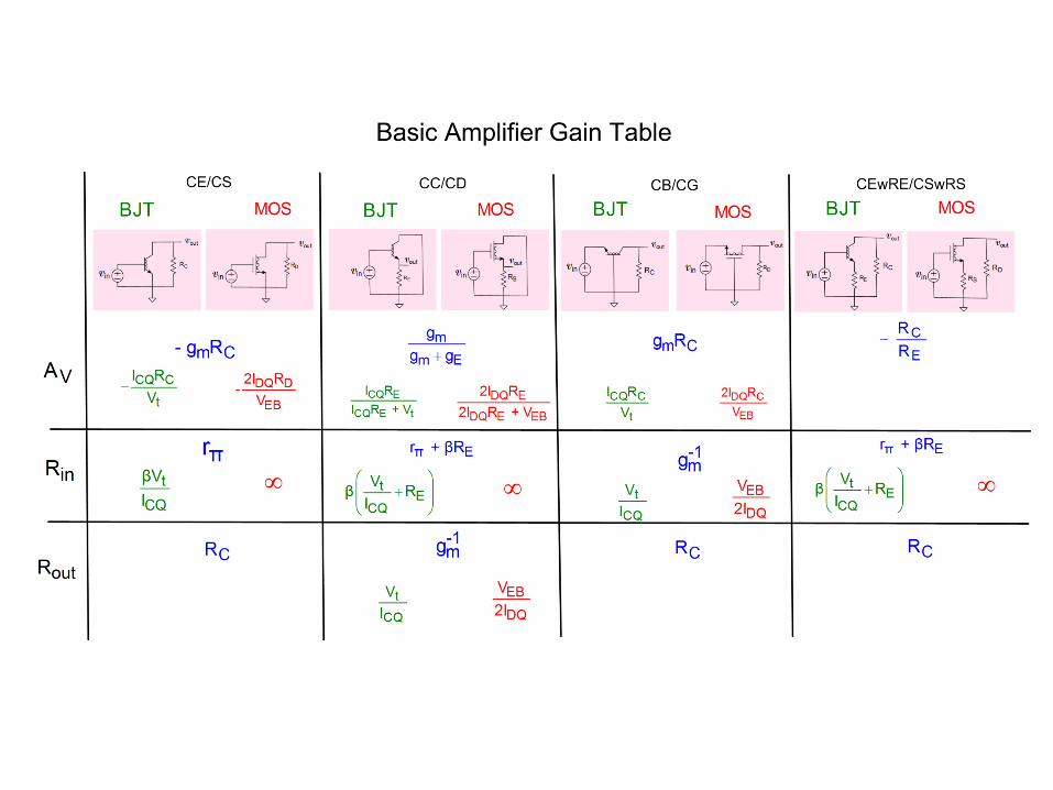
Basic Amplifier Structures
1. Common Emitter/Common Source 2. Common Collector/Common Drain 3. Common Base/Common Gate 4. Common Emitter with RE/ Common Source with RS
5. Cascode (actually CE:CB or CS:CD cascade) 6. Darlington (special CE:CE or CS:CS cascade)
The first 4 are most popular

Why are we focusing on these basic circuits?
1. So that we can develop analytical skills
2. So that we can design a circuit
3. So that we can get the insight needed to design a circuit
Which is the most important?

Why are we focusing on these basic circuits?
1. So that we can develop analytical skills
2. So that we can design a circuit
3. So that we can get the insight needed to design a circuit
Which is the most important?
1. So that we can get the insight needed to design a circuit
2. So that we can design a circuit
3. So that we can develop analytical skills
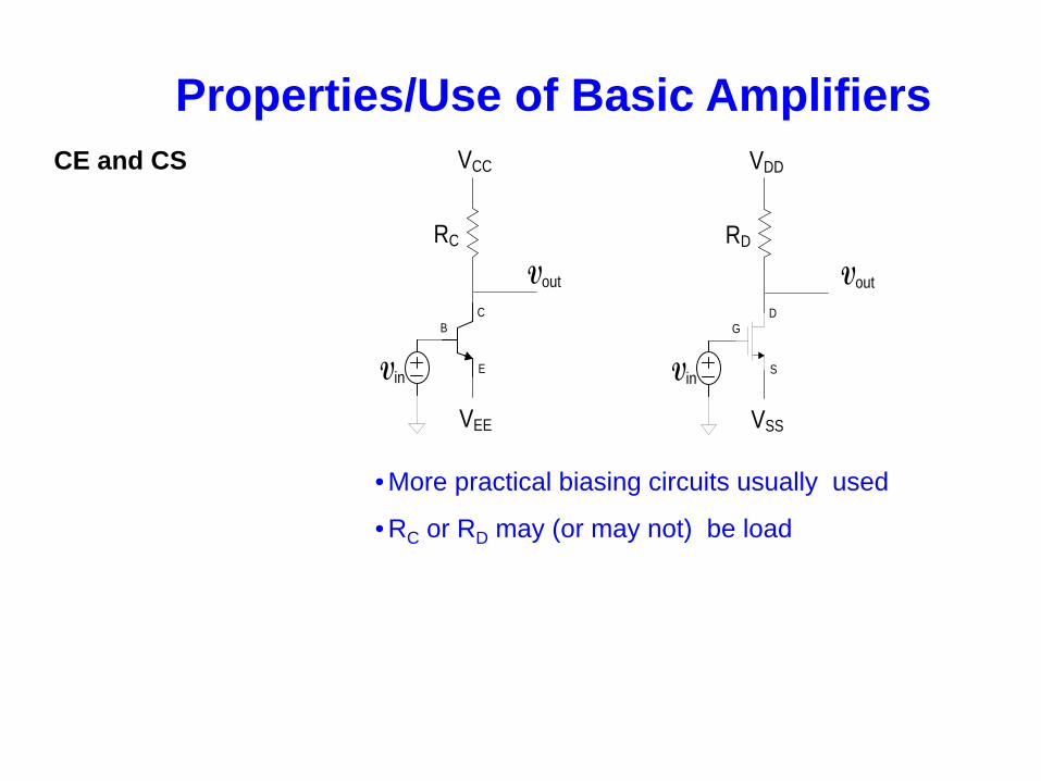
Properties/Use of Basic Amplifiers CE and CS
B
E
C
VCC
Vin
RC
Vout
VEE
G
S
D
VDD
Vin
RD
VSS
Vout
• More practical biasing circuits usually used
• RC or RD may (or may not) be load
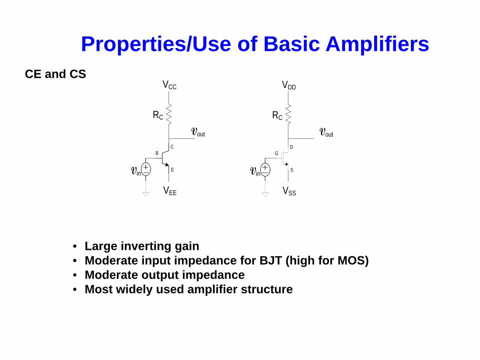
Properties/Use of Basic Amplifiers CE and CS
B
E
C
VCC
Vin
RC
Vout
VEE
G
S
D
VDD
Vin
RC
VSS
Vout
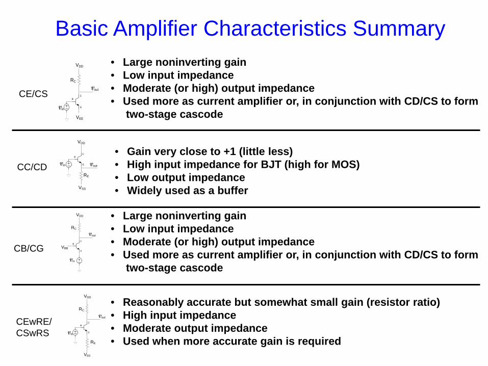
• Large inverting gain • Moderate input impedance for BJT (high for MOS) • Moderate output impedance • Most widely used amplifier structure
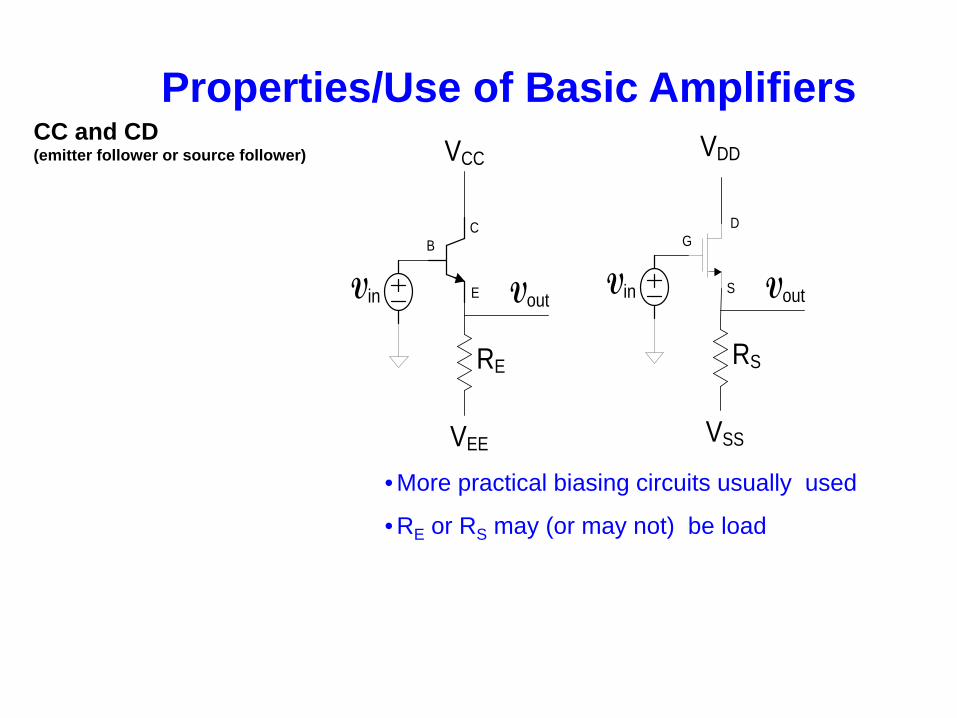
Properties/Use of Basic Amplifiers CC and CD (emitter follower or source follower)
B
E
C
VEE
VCC
Vin
RE
Vout
G
S
D
VSS
VDD
Vin
RS
Vout
• More practical biasing circuits usually used
• RE or RS may (or may not) be load
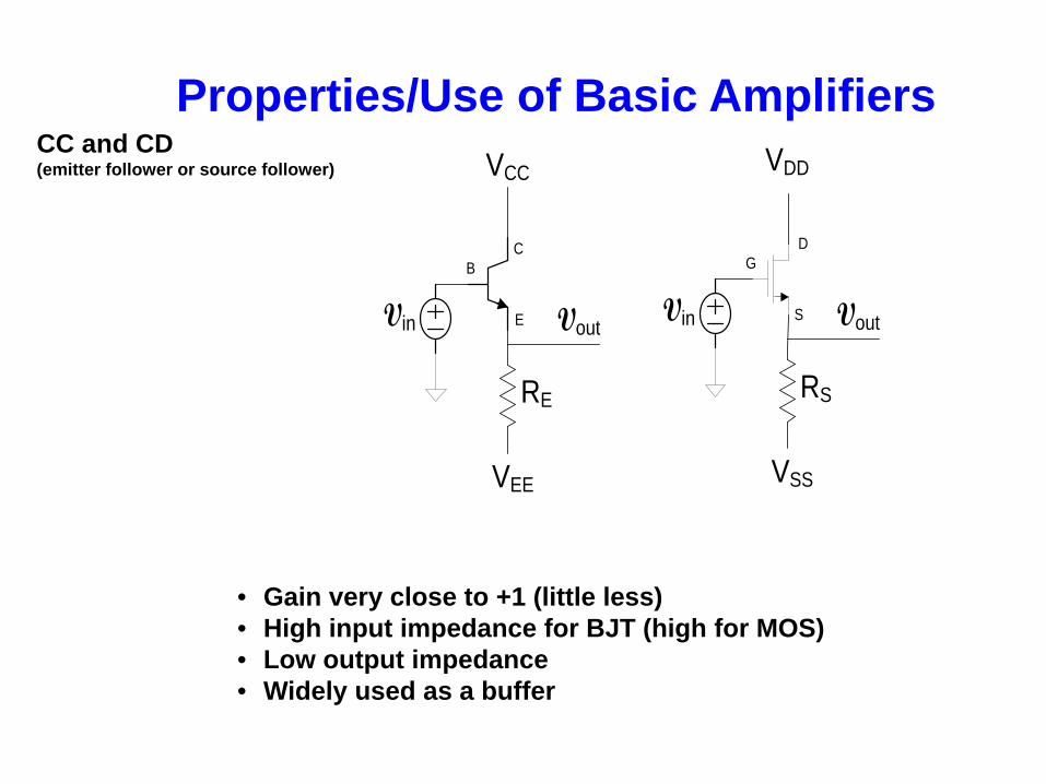
Properties/Use of Basic Amplifiers CC and CD (emitter follower or source follower)
B
E
C
VEE
VCC
Vin
RE
Vout
G
S
D
VSS
VDD
Vin
RS
Vout
• Gain very close to +1 (little less) • High input impedance for BJT (high for MOS) • Low output impedance • Widely used as a buffer
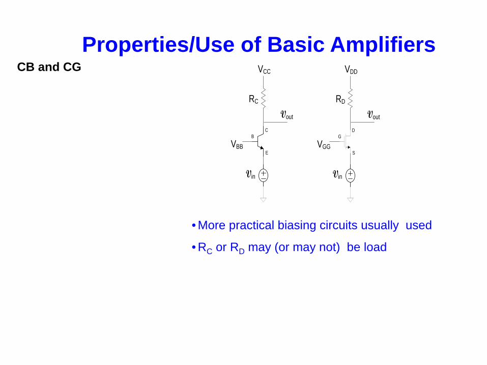
Properties/Use of Basic Amplifiers CB and CG
B
E
C
VBB
VCC
Vin
RC
Vout
G
S
D
VGG
VDD
Vin
RD
Vout
• More practical biasing circuits usually used
• RC or RD may (or may not) be load
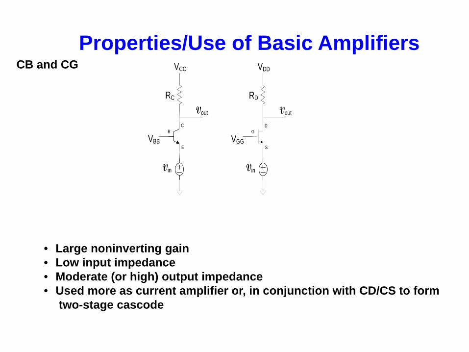
Properties/Use of Basic Amplifiers CB and CG
• Large noninverting gain • Low input impedance • Moderate (or high) output impedance • Used more as current amplifier or, in conjunction with CD/CS to form
two-stage cascode
B
E
C
VBB
VCC
Vin
RC
Vout
G
S
D
VGG
VDD
Vin
RD
Vout
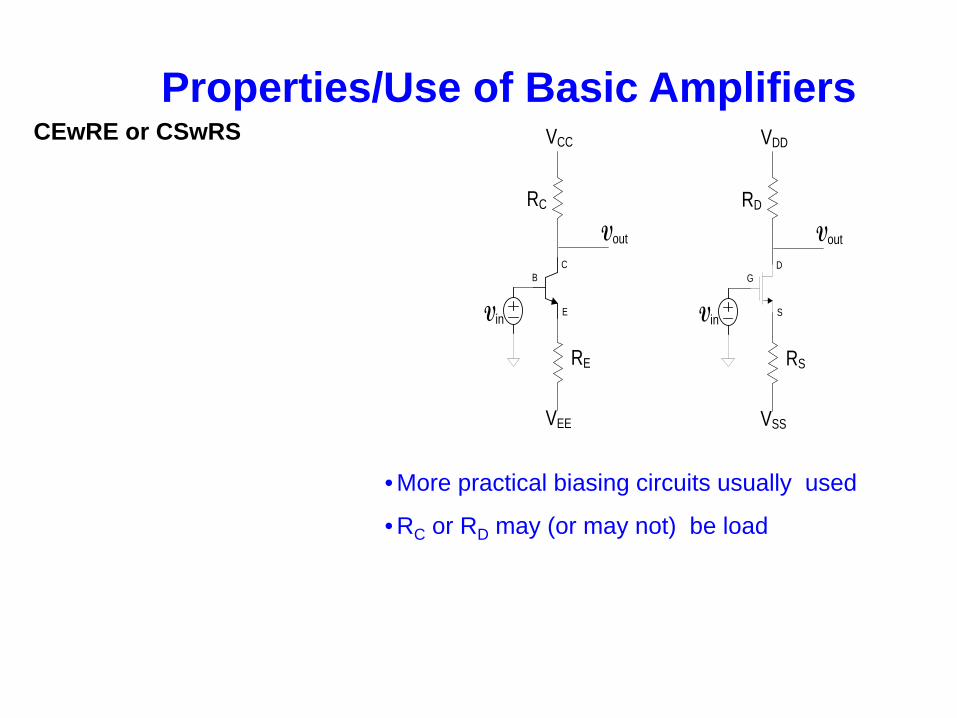
Properties/Use of Basic Amplifiers CEwRE or CSwRS
B
E
C
VCC
Vin
RC
Vout
RE
VEE
G
S
D
VDD
Vin
RD
Vout
RS
VSS
• More practical biasing circuits usually used
• RC or RD may (or may not) be load
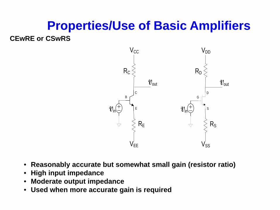
Properties/Use of Basic Amplifiers CEwRE or CSwRS
• Reasonably accurate but somewhat small gain (resistor ratio) • High input impedance • Moderate output impedance • Used when more accurate gain is required
B
E
C
VCC
Vin
RC
Vout
RE
VEE
G
S
D
VDD
Vin
RD
Vout
RS
VSS
B
E
C
VDD
Vin
RC
Vout
RE
VEE
B
E
C
VSS
VDD
Vin
RE
Vout
B
E
C
VDD
Vin
RC
Vout
VEE
B
E
C
VBB
VDD
Vin
RC
Vout
CE/CS
CC/CD
CB/CG
CEwRE/ CSwRS
Basic Amplifier Characteristics Summary
• Reasonably accurate but somewhat small gain (resistor ratio) • High input impedance • Moderate output impedance • Used when more accurate gain is required
• Large noninverting gain • Low input impedance • Moderate (or high) output impedance • Used more as current amplifier or, in conjunction with CD/CS to form
two-stage cascode
• Large noninverting gain • Low input impedance • Moderate (or high) output impedance • Used more as current amplifier or, in conjunction with CD/CS to form
two-stage cascode
• Gain very close to +1 (little less) • High input impedance for BJT (high for MOS) • Low output impedance • Widely used as a buffer
Cascaded Amplifier Analysis and Operation
RoX1V1 v01 1A V V2
RiX1 RL
RS
Vin
VoutRoX2
V3v02 3A V V4RiX2RL1
out iX1 L1 iX2 LV V01 V02
in iX1 S L1 iX2 0X1 L 0X2
R R //R RA A AR +R R //R +R R +R
= =
VV
Repeat from earlier discussions on amplifiers
Accounts for all loading between stages !
(applicable when all stages are unilateral)
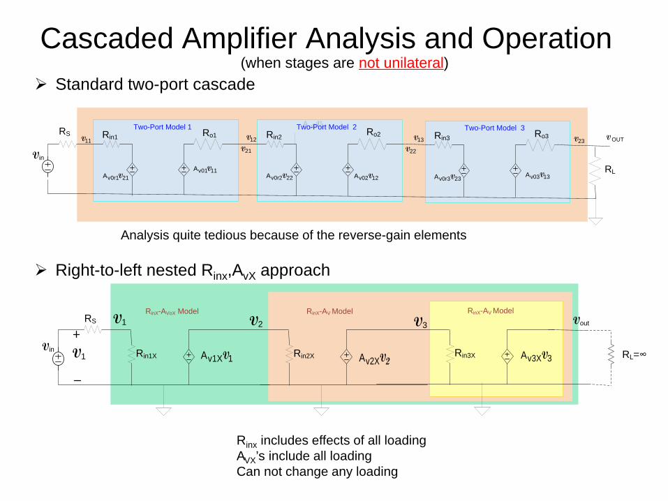
Cascaded Amplifier Analysis and Operation (when stages are not unilateral)
Ro1v0 1A V
Rin1
v0r1 21A V
Two-Port Model 1 Ro2
v02 12A V
Rin2
v0r2 22A V
Two-Port Model 2Ro3
v03 13A V
Rin3
v0r3 23A V
Two-Port Model 3
RL
OUT V23 V13 V
22 V
12 V
21 V
v01 11A V
11 VRS
Vin
Analysis quite tedious because of the reverse-gain elements
Right-to-left nested Rinx,AvX approach
Standard two-port cascade
Rinx includes effects of all loading AVX’s include all loading Can not change any loading
V1 v1X 1A VRin1XVin
RSRinX-AVoX Model
v3X 3A VRin3X
RinX-AV ModelVout
RL=∞v2XA 2VRin2X
RinX-AV ModelV3V2V1

End of Lecture 33