Embed Size (px)
Citation preview
1
BIPOLARJUNCTIONTRANSISTORSLAB7:INTRODUCTIONTOTRANSISTORAMPLIFERSANDMAKINGANAUDIOAMPLIFIER
DEFINITIONShfeorβ –transistorcurrentgainintrinsictothetransistoritself.VE,VB,VC–voltagesattheemitter,base,andcollector,respectively.
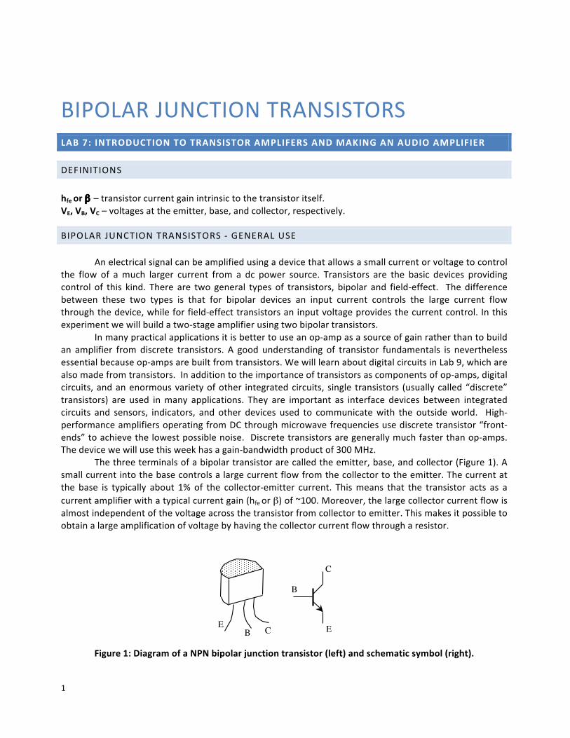
BIPOLARJUNCTIONTRANSISTORS-GENERALUSE Anelectricalsignalcanbeamplifiedusingadevicethatallowsasmallcurrentorvoltagetocontrolthe flow of amuch larger current from a dc power source. Transistors are the basic devices providingcontrol of this kind. There are two general types of transistors, bipolar and field-effect. The differencebetween these two types is that for bipolar devices an input current controls the large current flowthroughthedevice,whileforfield-effecttransistorsaninputvoltageprovidesthecurrentcontrol. Inthisexperimentwewillbuildatwo-stageamplifierusingtwobipolartransistors. Inmanypracticalapplicationsitisbettertouseanop-ampasasourceofgainratherthantobuildan amplifier from discrete transistors. A good understanding of transistor fundamentals is neverthelessessentialbecauseop-ampsarebuiltfromtransistors.WewilllearnaboutdigitalcircuitsinLab9,whicharealsomadefromtransistors.Inadditiontotheimportanceoftransistorsascomponentsofop-amps,digitalcircuits,andanenormousvarietyofother integratedcircuits, single transistors (usuallycalled“discrete”transistors) are used inmany applications. They are important as interface devices between integratedcircuits and sensors, indicators, and other devices used to communicatewith the outsideworld. High-performanceamplifiersoperatingfromDCthroughmicrowavefrequenciesusediscretetransistor“front-ends”toachievethelowestpossiblenoise.Discretetransistorsaregenerallymuchfasterthanop-amps.Thedevicewewillusethisweekhasagain-bandwidthproductof300MHz. Thethreeterminalsofabipolartransistorarecalledtheemitter,base,andcollector(Figure1).Asmallcurrentintothebasecontrolsalargecurrentflowfromthecollectortotheemitter.Thecurrentatthe base is typically about 1% of the collector-emitter current. Thismeans that the transistor acts as acurrentamplifierwithatypicalcurrentgain(hfeorβ)of~100.Moreover,thelargecollectorcurrentflowisalmostindependentofthevoltageacrossthetransistorfromcollectortoemitter.Thismakesitpossibletoobtainalargeamplificationofvoltagebyhavingthecollectorcurrentflowthrougharesistor.
Figure1:DiagramofaNPNbipolarjunctiontransistor(left)andschematicsymbol(right).
Figure 7.1 Pin-out of 2N3904 and 1 k trimpot
EB C E
B
C
cw
ccwwiper
ccw
wiper
cw
2
CURRENTAMPLIFIERMODELOFABIPOLARTRANSISTOR Fromthesimplestpointofviewabipolartransistorisacurrentamplifier.Thecurrentflowingfromcollectortoemitterisequaltothebasecurrentmultipliedbyafactor.Annpntransistorlikethe2N3904operateswiththecollectorvoltageat leasta fewtenthsofavoltabovetheemitter,andwithacurrentflowing into the base (There are also pnp transistorswith opposite polarity voltages and currents). Thebase-emitterjunctionthenactslikeaforward-biaseddiodewitha0.6Vdrop:VB≈ VE+0.6V.Undertheseconditions,thecollectorcurrentisproportionaltothebasecurrent:IC=hfeIB. The constant of proportionality (‘current gain’) is called hfe because it is one of the "h-parameters," a set of numbers that give a complete description of the small-signal properties of atransistor.Itisimportanttokeepinmindthathfeisnotreallyaconstant.Itdependsoncollectorcurrent(seeH&HFig.2.78),anditvariesby50%ormorefromdevicetodevice.Ifyouwanttoknowtheemittercurrentratherthanthecollectorcurrentyoucanfinditbycurrentconservation:IE=IB+IC=(1/hfe+1)IC.ThedifferencebetweenICandIEisalmostneverimportantsincehfeisnormallyintherange100–1000.Another way to say this is that the base current is very small compared to the collector and emittercurrents.
EMITTERFOLLOWERANDCOMMONEMITTERAMPLIFIERS Wewillbeginbyconstructingacommonemitteramplifier,whichoperateson theprincipleofacurrentamplifier.Amajorfaultofasingle-stagecommonemitteramplifier is itshighoutputimpedance.(Rememberwhythisisaproblem?ThinkvoltagedividerandOhm’sLaw.)Thisproblemcanbeaddressedbyaddinganemitterfollowerasasecondstage.Intheemitterfollowercircuit,thecontrolsignalisagainappliedat thebase,but theoutput is takenfromtheemitter. Theemittervoltageprecisely followsthebasevoltage,butmorecurrentisavailablefromtheemitter.Thecommon-emitterstageandtheemitterfollowerstagearethemostcommonbipolartransistorcircuitconfigurations.
3
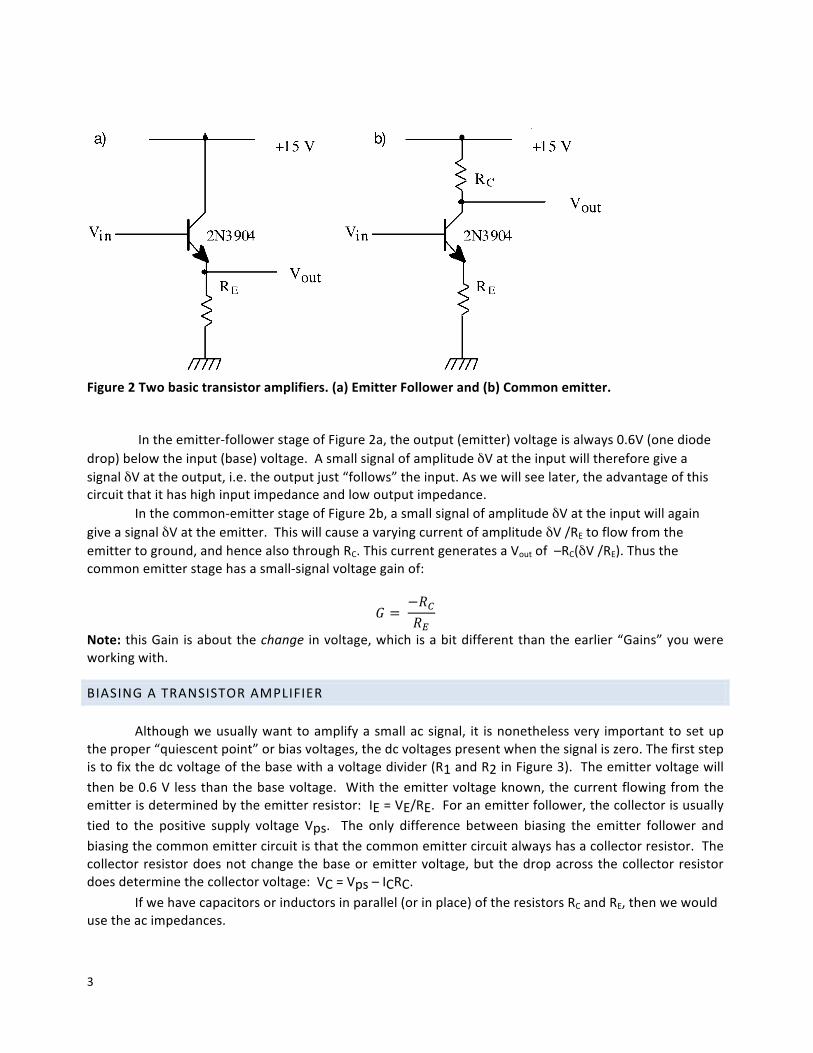
Figure2Twobasictransistoramplifiers.(a)EmitterFollowerand(b)Commonemitter.
Intheemitter-followerstageofFigure2a,theoutput(emitter)voltageisalways0.6V(onediodedrop)belowtheinput(base)voltage.AsmallsignalofamplitudeδVattheinputwillthereforegiveasignalδVattheoutput,i.e.theoutputjust“follows”theinput.Aswewillseelater,theadvantageofthiscircuitthatithashighinputimpedanceandlowoutputimpedance. Inthecommon-emitterstageofFigure2b,asmallsignalofamplitudeδVattheinputwillagaingiveasignalδVattheemitter.ThiswillcauseavaryingcurrentofamplitudeδV/REtoflowfromtheemittertoground,andhencealsothroughRC.ThiscurrentgeneratesaVoutof–RC(δV/RE).Thusthecommonemitterstagehasasmall-signalvoltagegainof:
𝐺 = −𝑅!𝑅!
Note: thisGain isaboutthechange involtage,which isabitdifferentthantheearlier“Gains”youwereworkingwith.
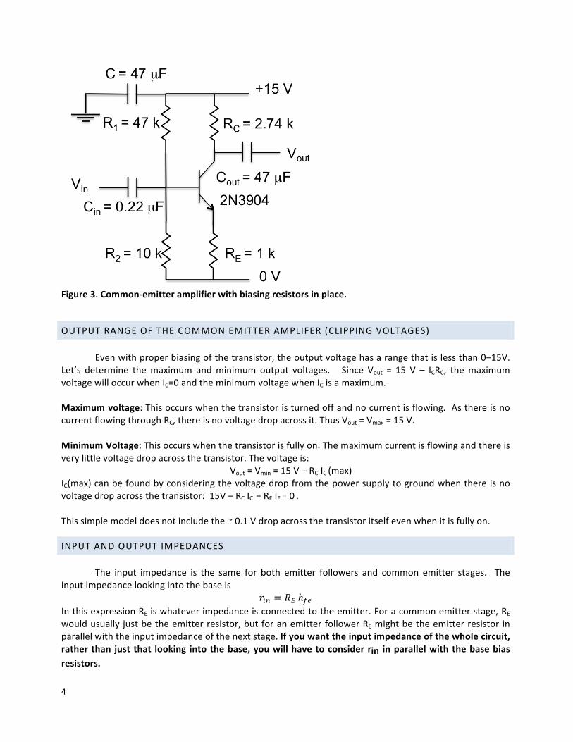
BIASINGATRANSISTORAMPLIFIER Althoughweusuallywanttoamplifyasmallacsignal, it isnonethelessvery importanttosetuptheproper“quiescentpoint”orbiasvoltages,thedcvoltagespresentwhenthesignaliszero.Thefirststepistofixthedcvoltageofthebasewithavoltagedivider(R1andR2inFigure3).Theemittervoltagewillthenbe0.6V lessthanthebasevoltage. Withtheemittervoltageknown,thecurrentflowingfromtheemitterisdeterminedbytheemitterresistor:IE=VE/RE.Foranemitterfollower,thecollectorisusuallytied to the positive supply voltage Vps. The only difference between biasing the emitter follower andbiasingthecommonemittercircuitisthatthecommonemittercircuitalwayshasacollectorresistor.Thecollectorresistordoesnotchangethebaseoremittervoltage,butthedropacrossthecollectorresistordoesdeterminethecollectorvoltage:VC=Vps–ICRC. Ifwehavecapacitorsorinductorsinparallel(orinplace)oftheresistorsRCandRE,thenwewouldusetheacimpedances.
4
Figure3.Common-emitteramplifierwithbiasingresistorsinplace.
OUTPUTRANGEOFTHECOMMONEMITTERAMPLIFER(CLIPPINGVOLTAGES) Evenwithproperbiasingofthetransistor,theoutputvoltagehasarangethatislessthan0−15V.Let’s determine themaximum andminimum output voltages. Since Vout = 15 V – ICRC, themaximumvoltagewilloccurwhenIC=0andtheminimumvoltagewhenICisamaximum.Maximumvoltage:Thisoccurswhenthetransistoristurnedoffandnocurrentisflowing.AsthereisnocurrentflowingthroughRC,thereisnovoltagedropacrossit.ThusVout=Vmax=15V.MinimumVoltage:Thisoccurswhenthetransistorisfullyon.Themaximumcurrentisflowingandthereisverylittlevoltagedropacrossthetransistor.Thevoltageis: Vout=Vmin=15V–RCIC(max)IC(max)canbefoundbyconsideringthevoltagedropfromthepowersupplytogroundwhenthereisnovoltagedropacrossthetransistor:15V–RCIC−REIE=0.Thissimplemodeldoesnotincludethe~0.1Vdropacrossthetransistoritselfevenwhenitisfullyon.
INPUTANDOUTPUTIMPEDANCES The input impedance is the same for both emitter followers and common emitter stages. Theinputimpedancelookingintothebaseis
𝑟!" = 𝑅! ℎ!" InthisexpressionREiswhateverimpedanceisconnectedtotheemitter.Foracommonemitterstage,RE
wouldusually justbetheemitterresistor,butforanemitterfollowerREmightbetheemitterresistor inparallelwiththeinputimpedanceofthenextstage.Ifyouwanttheinputimpedanceofthewholecircuit,rather than just that looking intothebase,youwillhavetoconsiderrin inparallelwiththebasebiasresistors.
5
Theoutputimpedanceofacommonemitterstage(Fig.2b)aloneisjustequaltothecollectorresistorRC.
𝑟!"# = 𝑅! (commonemitterstage)Theoutputimpedancelookingintotheemitterofanemitterfollower(e.g.Fig.2a)isgivenby
𝑟!"# =!!
!!"!!(emitterfollowerstage)
RB stands for whatever impedance is connected to the base. Usually this impedance is in parallel with whateverimpedanceisconnectedtotheemitter(RE).
EBERS-MOLLMODELOFABIPOLARTRANSISTOR Aslightlymorecompletemodelofthebipolartransistorisrequiredtounderstandwhathappenswhentheemitterresistorisverysmall.Insteadofusingthecurrentamplifiermodel,onecantaketheviewthatthecollectorcurrentICiscontrolledbythebase-emittervoltageVBE.Forourpurposes,theEbers-Mollmodelmodifiesourcurrentamplifiermodelofthetransistorinonlyoneimportantway.Forsmallvariationsaboutthequiescentpoint,thetransistornowactsasifithasasmallinternalresistor,re,inserieswiththeemitter.Themagnitudeoftheintrinsicemitterresistance,re,dependsonthecollectorcurrentIC.
𝑟! = 25Ω 1 𝑚𝐴𝐼!
Thepresenceoftheintrinsicemitterresistance,re,modifiestheaboveequationsasfollows.
𝑟!" = (𝑅! + 𝑟!)ℎ!"
𝑟!"# =!!
!!"!!+ 𝑟! (emitterfollowerstage)
Themostimportantoftheseresultsisthemodifiedgain:
𝐺 = −𝑅!𝑅! + 𝑟!
whichshowsthatthecommonemittergainisnotinfinitewhentheexternalemitterresistorgoestozero.
USEFULREADINGS1. Diefenderfer&Holton8.1–8.42. Adatasheetforthe2N3904transistorispostedonourcoursewebsite.3. HorowitzandHill,Chapter2. Themost importantsectionsare2.01–2.03,2.05, thefirstpageof
2.06,2.07,2.09–2.12,andthepartof2.13onpage84and85.HavealookatTable2.1andFigure2.78forasummaryofthespecificationsofsomerealdevices.
LABPREPACTIVITIES
AnswerthefollowingquestionsusingMathematicaorbyhandinyourlabbook.Bringanelectroniccopyofyournotebooktolab,preferablyonyourownlaptop.
6
Question1
Biasingthetransistora. Calculatethequiescentvoltages(theDCvoltageswithnosignalpresent)VB,VE,and
VC and the currents IE and IC for the commonemitter circuit in Figure 3. Youmayassumethathfeissolargethatthebasecurrentisnegligible.
b. Howmuchpowerisdissipatedinthetransistoritself?IsthepowersafelybelowPmax?See2N3904datasheetpostedonourwebsite.
c. Whatisthepurposeoftheinputandoutputcapacitors,CinandCout?
Question2
Transistoramplifier–singlestage(commonemitter)a. What is themaximumhfevalueat10mAcollectorcurrent?See2N3904datasheet
postedonourwebsite.(Youmayusethisvalueforcalculationsbelow.)b. WhatistheacvoltagegainofthecircuitinFigure3for15kHzsinewaves?c. Whatarethemaximumandminimumpossibleoutputvoltages?d. For thesingle stage inFigure3,whatare the inputandoutput impedances rinand
routat15kHz?NotethattheinputimpedanceofthecommonemitterwiththebiasresistornetworkistheinputresistanceofthecommonemitterinparallelwithbothR1andR2.Thatis,rin(total)=rin(commonemitter)||R1||R2.
e. Calculate the fraction of the original amplitude obtained when a 560 Ω load isconnectedtotheoutputviaacouplingcapacitor(Cout inFig.3)toground.HINT:the560Ω resistorwill be in serieswith theoutput impedanceof the circuit to ground.Even at only 15 kHz, the output capacitor acts as a wire for the ac impedance. ItservestoblockonlytheDCvoltage.
Question3
Transistoramplifier–dualstage(commonemitter+emitterfollower)a. What is the ac voltage gain of the entire dual-stage amplifier (common emitter +
emitterfollower)circuitinFigure4for15kHzsinewaves?b. FortheentiredualstageamplifierinFigure4,whatistheoutputimpedanceroutat
15kHz? HINT: The impedance at the base of the emitter follower is the collectorresistorofthecommonemitter.
f. Calculate the fraction of the original amplitude obtained when a 560 Ω load isconnected to the output via a coupling capacitor (Cout in Fig. 4).HINT: the 560Ωresistorwillbe inserieswiththeoutput impedanceofthecircuit toground.Evenatonly 15 kHz, the output capacitor acts as awire for the ac impedance. It serves toblockonlytheDCvoltage.
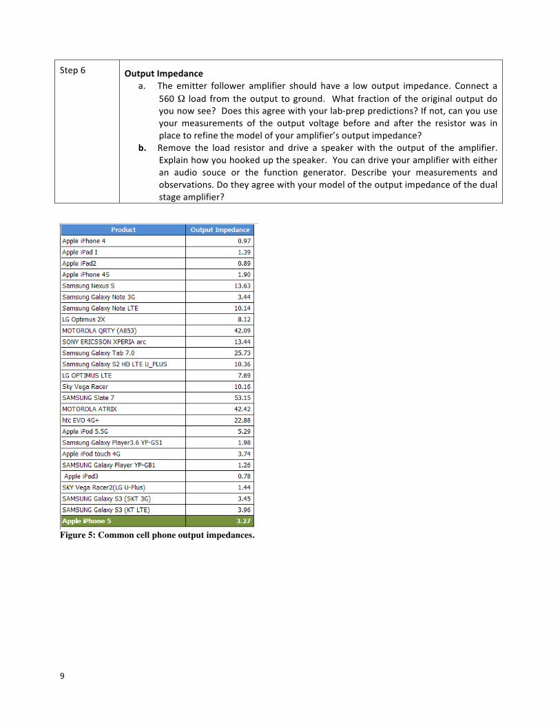
Question4 AudioAmplifiera. Whatistheoutputimpedanceofyourphone(orpartner’sphone)?SeeFigure5.b. Astandardnon-amplifiedspeakerhasaninputimpedanceof8Ω.Ifyourphonehad
anoutputvoltageat1Vunloaded,whatwouldtheloadedvoltagebeifyouhookedituptothe8Ωspeaker?HINT:Thinkvoltagedivider.
c. Now,insteadyoucanusethecommonemittertoamplifythesignalfromyourphonefirst. If your common emitter amplifier has an unloaded output voltage of 2.7 V(assumingagainof2.7),whatistheoutputvoltageifyouconnectan8Ωspeakertotheamplifier?HINT:Thinkvoltagedividerwiththeoutputimpedanceofthecommonemitter.
d. Finally,considerusingthetwo-stageamplifiershowninfigure4todrivethespeaker.Iftheemitterfolloweramplifieroutputstagehasanunloadedoutputvoltageof2.7V(assumingagainof2.7),whatistheoutputvoltageifyouconnectan8Ωspeakertotheamplifier?HINT:Thinkvoltagedividerwiththeoutput impedanceoftheemitterfollower.
7
Question5 Labactivitiesa. Readthroughallofthelabstepsandidentifythestep(orsub-step)thatyouthinkwill
bethemostchallenging.b. Listatleastonequestionyouhaveaboutthelabactivity.
COMMOMEMITTERAMPLIFIER
Step1
QuiescentState a. BuildthecommonemitteramplifiershowninFigure3(withoutthecapacitorsCin
andCout)andcheckthatthecorrectdclevels(quiescentvoltages)areestablished.Measure the resistorsbeforeputting them in thecircuit, and if theydiffer fromthevaluesusedinyourcalculations,recalculatethepredictedquiescentvoltages.Drawthecircuitschematic inyour labbookand labelall components.Whatarethe dc levels VB (at the transistor base), VE (at the emitter) and VC (at thecollector)?Dotheyagreewithyourpredictions?
Step2 LowfrequencyACGaina. ConvertthepreviouscircuittoanACamplifierbyaddingthecouplingcapacitors
CinandCout.Makesuretogetthepolaritycorrect(forCout,considergroundontheright).Thecapacitorswilltransmitacsignalsbutblockdcsignals.Thisallowsyoutoconnectsignalswithoutdisturbingthequiescentconditions.
b. When you switch on the power, you may see high frequency spontaneousoscillations. These must be suppressed before you can proceed. An additionalbypasscapacitor(~100nF)between+15Vandgroundclosetothetransistormayhelp.Also,reducingthelengthofyourcircuitwirescanhelp.
c. Assembleatestset-uptoobservethe inputandoutputoftheamplifierwith15kHzsinewaves,usingthe10xscopeprobefortheoutput.HINT:Youmayneedtoadda220kΩresistortogroundafterCouttokeepthedclevelatthescopeinputnear ground as the large output capacitor can slowly charge up. Youmay alsowanttoputthescopeonaccouplingwhenyouprobepointswithlargedcoffsetsbutswitchitbacktoDCifyouwanttomeasurequiescentvoltages.Varytheinputamplitude todetermine theoutputamplitudeatwhich clippingbegins. Youwillwant to stay below half of this clipping voltage to assure the amplifier is notdistortingtheoutputwaveform.
d. Measurethegainoftheamplifierfor15kHzsinewaves.Doesyourmeasurementagreewithyourprediction?
Step3 OutputImpedancea. The common emitter amplifier often has a large output impedance. Connect a
560Ω load fromtheoutput toground. What fractionof theoriginaloutputdoyounowsee?Doesthisagreewithyourlab-preppredictions?Ifnot,canyouuseyourmeasurements of the output voltage before and after the resistor was inplacetorefinethemodelofyouramplifier’soutputimpedance?
b. Remove the load resistor and drive a speakerwith the output of the amplifier.Explainhowyouhookedupthespeaker.Firstdrivethecircuitwiththefunctiongenerator. Describe your measurements and observations. Do they agree withyour model of the output impedance of the common emitter amplifier?HINT:
8
Consider themaximumandminimumoutput voltagespossible you calculated intheprelab.
c. Now drive the circuit with an audio source. Describe your measurements andobservations.
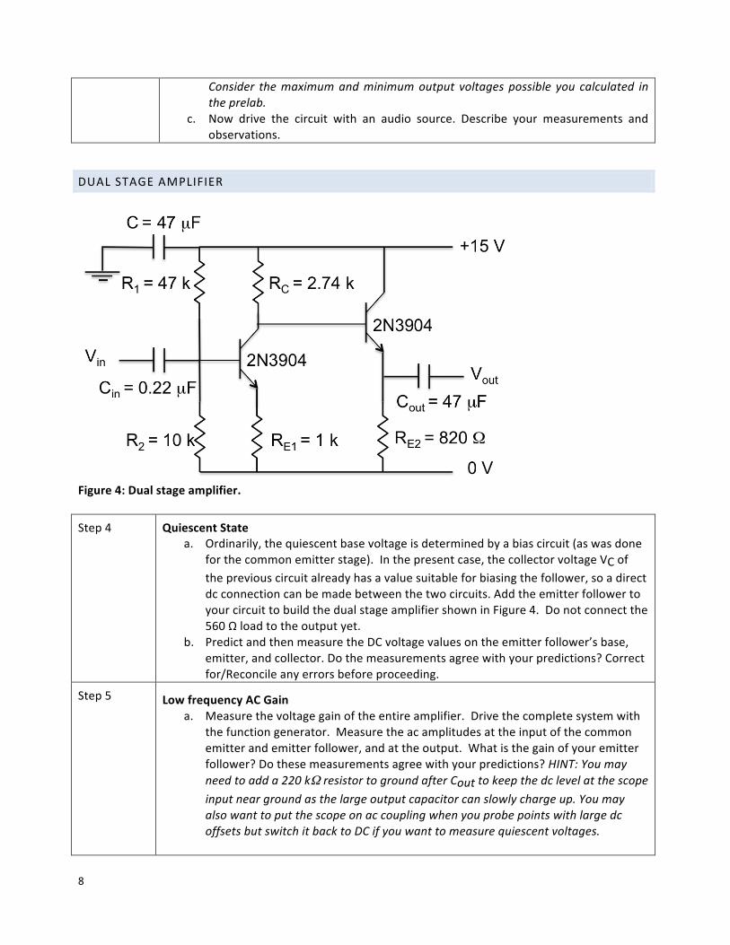
DUALSTAGEAMPLIFIER
Figure4:Dualstageamplifier.
Step4
QuiescentState a. Ordinarily,thequiescentbasevoltageisdeterminedbyabiascircuit(aswasdone
forthecommonemitterstage).Inthepresentcase,thecollectorvoltageVCofthepreviouscircuitalreadyhasavaluesuitableforbiasingthefollower,soadirectdcconnectioncanbemadebetweenthetwocircuits.AddtheemitterfollowertoyourcircuittobuildthedualstageamplifiershowninFigure4.Donotconnectthe560Ωloadtotheoutputyet.
b. PredictandthenmeasuretheDCvoltagevaluesontheemitterfollower’sbase,emitter,andcollector.Dothemeasurementsagreewithyourpredictions?Correctfor/Reconcileanyerrorsbeforeproceeding.
Step5 LowfrequencyACGaina. Measurethevoltagegainoftheentireamplifier.Drivethecompletesystemwith
thefunctiongenerator.Measuretheacamplitudesattheinputofthecommonemitterandemitterfollower,andattheoutput.Whatisthegainofyouremitterfollower?Dothesemeasurementsagreewithyourpredictions?HINT:Youmayneedtoadda220kΩresistortogroundafterCouttokeepthedclevelatthescopeinputneargroundasthelargeoutputcapacitorcanslowlychargeup.YoumayalsowanttoputthescopeonaccouplingwhenyouprobepointswithlargedcoffsetsbutswitchitbacktoDCifyouwanttomeasurequiescentvoltages.
9
Step6 OutputImpedancea. The emitter follower amplifier should have a low output impedance. Connect a
560Ω load fromtheoutput toground. What fractionof theoriginaloutputdoyounowsee?Doesthisagreewithyourlab-preppredictions?Ifnot,canyouuseyour measurements of the output voltage before and after the resistor was inplacetorefinethemodelofyouramplifier’soutputimpedance?
b. Remove the load resistor and drive a speaker with the output of the amplifier.Explainhowyouhookedupthespeaker.Youcandriveyouramplifierwitheitheran audio souce or the function generator. Describe your measurements andobservations.Dotheyagreewithyourmodeloftheoutputimpedanceofthedualstageamplifier?
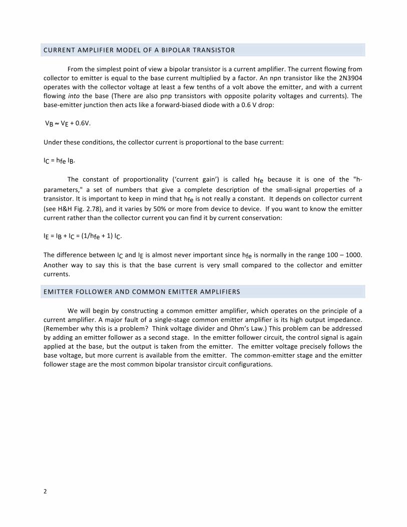
Figure 5: Common cell phone output impedances.