Embed Size (px)
Citation preview
INVESTIGACION REVISTA MEXICANA DE FISICA 55 (5) 347–353 OCTUBRE 2009
Bode plots applied to microscopic interferometry
J.M. Flores, M. Cywiak*, M. Servın, and L. JuarezCentro de Investigaciones enOptica, A.C.,
Loma del Bosque 115, Lomas del Campestre, Leon, Guanajuato, 37150 Mexico,∗e-mail: [email protected]
Recibido el 16 de junio de 2008; aceptado el 7 de septiembre de 2009
We describe a technique for using Bode plots in microscopic interferometry, in particular as applied to the three Gaussian beam interferometerrecently reported in the literature. The technique is used in a similar manner to its application to an electric or electronic system in findingits frequency response. The Bode response is used to deconvolve the raw data obtained directly from the interferometer to compensate forthe data in frequency, making it possible to obtain more realistic profiles of the samples under test. We apply this technique to obtain profilesof the inner reflective layers of two optical types of surfaces for data storage commercially available, namely, the compact disk (CD-R) andthe digital versatile disk (DVD-R). We report the experimental results of radial scans of these devices without data marks, before and afterapplying the transfer function of the system. The measurements are obtained by placing the devices with the polycarbonate surfaces so asto aim the probe beam of the interferometer at them, taking advantage of the vertical depth discrimination of the microscope. We show thatthe resulting profiles, obtained across the Polycarbonate layer, measured with this interferometer, give valuable information of the real trackprofiles, making the combination of the Bode plots with this interferometer a suitable tool for quality control of the surface storage devices.
Keywords: Bode transform; gaussian beam; interferometry.
Describimos una tecnica que permite utilizar las graficas de Bode en interferometrıa microscopica, en particular aplicada al interferometrode tres haces Gaussianos recientemente reportado en la literatura. La tecnica es utilizada de una manera similar a la forma en que sehace para encontrar la respuesta en frecuencia de un sistema electrico o electronico. La respuesta de Bode es utilizada para calcular ladeconvolucion de los datos crudos obtenidos directamente del interferometro para compensar los datos en frecuencia, permitiendo obtenerun perfil mas realista de las muestras bajo prueba. Aplicamos la tecnica para obtener los perfiles de las superficies reflectoras internas dedos dispositivosopticos comercialmente disponibles para almacenamiento de datos, el disco compacto (CD-R) y el disco digital versatil(DVD-R). Reportamos resultados experimentales de una exploracion radial de estos dispositivos sin datos almacenados, antes y despues deaplicar la funcion de transferencia del sistema. Las mediciones son obtenidas colocando los dispositivos con la superficie de Policarbonatoapuntando al haz de prueba del interferometro, aprovechando la ventaja de la discriminacion de profundidad del microscopio. Mostramos quelos perfiles resultantes, obtenidos a traves de la capa del Policarbonato, medidos con este interferometro, proporcionan informacion valiosade los perfiles reales de las pistas de estos dispositivos, por lo que la combinacion de Bode aunada al uso de este interferometro representanuna herramienta adecuada para el control de calidad de los dispositivosopticos de almacenamiento de datos mencionados.
Descriptores: Bode transform; gaussian beam; interferometry.
PACS: 07.60.; 42.79.Vb; 42.87.d
1. Introduction
Bode plots represent a useful tool for determining and analyz-ing the frequency response of an electronic or electrical sys-tem. These plots make it possible to detect important prop-erties of the response of a system, for example, resonancefrequencies. Two types of Bode plots are commonly used,namely magnitude vs. frequency, and phase vs. frequency.In this report, we are interested in the first plot.
Bode plots are based on the poles and zeros of a systemand are commonly used in feedback theory. In addition, theshape of the frequency response of the system makes it pos-sible to compensate for the resulting outputs by means of adeconvolution process. The magnitude versus frequency re-sponse is called the transfer function of the system and it isobtained simply by finding many frequency values, calculat-ing the magnitude of the output at each frequency and chart-ing them against a frequency coordinate.
It can be said in summary, as described in Refs. 1 and 2,that Bode plots represent two main aspects:
- They compress the spectral information of the functionalong the spectral axis. This permits the measurementof the dangerous (undamped) frequencies of a givensystemi.e., the poles of the frequency response func-tion.
- The above information of the dangerous frequencies isimportant for anticipating the noise and stability per-formance of the system.
For applying the Bode method to an optical system, inthis report, we have chosen the three-Gaussian beam interfer-ometer (TGBI) [3]. We have selected this interferometer be-cause it exhibits a Gaussian transfer function, centered at theorigin, thus making it simple to perform the process of decon-volution. We present the methodology for finding the Bodeplots for the TGBI by measuring several reflecting gratingswith different pitches, commercially available. The techniquepresented here is intended to be used in any interferometricmicroscope by using a set of calibrated gratings, in analogywith the sweep generator used in electronics.
348 J.M. FLORES, M. CYWIAK, M. SERVIN, AND L. JUAREZ
The presentation of this report is as follows. In the nextsection we describe the TGBI, which consists on of the het-erodyning of three beams with a Gaussian intensity profile.In sub-Sec. 2.1 our proposal to obtain the Bode responseis described and then applied for measuring the profiles oftwo optical storage devices, a CD and a DVD without datamarks. In Sec. 3, we present the experimental results of themeasurements of the profiles of the optical devices. Finally,our conclusions are presented in Sec. 4.
2. The three Gaussian beam interferometer
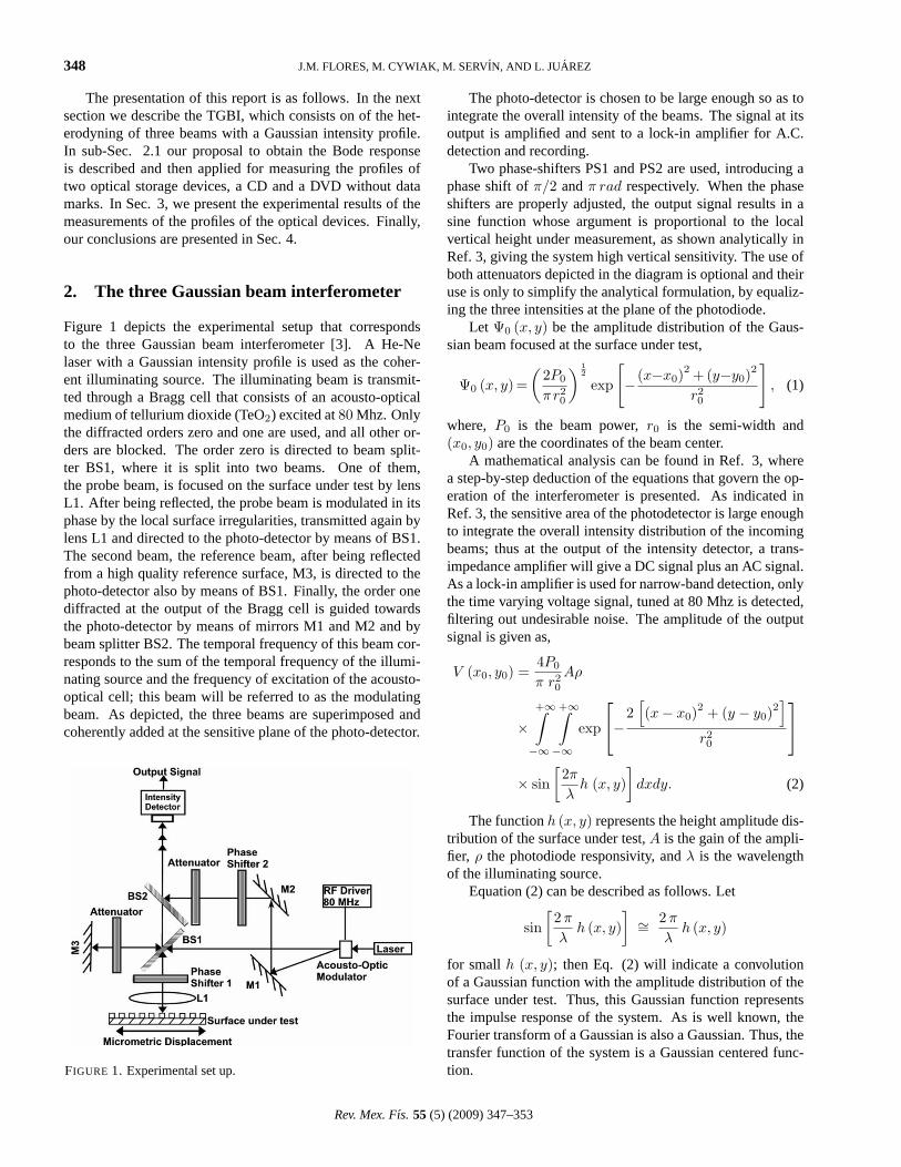
Figure 1 depicts the experimental setup that correspondsto the three Gaussian beam interferometer [3]. A He-Nelaser with a Gaussian intensity profile is used as the coher-ent illuminating source. The illuminating beam is transmit-ted through a Bragg cell that consists of an acousto-opticalmedium of tellurium dioxide (TeO2) excited at80 Mhz. Onlythe diffracted orders zero and one are used, and all other or-ders are blocked. The order zero is directed to beam split-ter BS1, where it is split into two beams. One of them,the probe beam, is focused on the surface under test by lensL1. After being reflected, the probe beam is modulated in itsphase by the local surface irregularities, transmitted again bylens L1 and directed to the photo-detector by means of BS1.The second beam, the reference beam, after being reflectedfrom a high quality reference surface, M3, is directed to thephoto-detector also by means of BS1. Finally, the order onediffracted at the output of the Bragg cell is guided towardsthe photo-detector by means of mirrors M1 and M2 and bybeam splitter BS2. The temporal frequency of this beam cor-responds to the sum of the temporal frequency of the illumi-nating source and the frequency of excitation of the acousto-optical cell; this beam will be referred to as the modulatingbeam. As depicted, the three beams are superimposed andcoherently added at the sensitive plane of the photo-detector.
FIGURE 1. Experimental set up.
The photo-detector is chosen to be large enough so as tointegrate the overall intensity of the beams. The signal at itsoutput is amplified and sent to a lock-in amplifier for A.C.detection and recording.
Two phase-shifters PS1 and PS2 are used, introducing aphase shift ofπ/2 andπ rad respectively. When the phaseshifters are properly adjusted, the output signal results in asine function whose argument is proportional to the localvertical height under measurement, as shown analytically inRef. 3, giving the system high vertical sensitivity. The use ofboth attenuators depicted in the diagram is optional and theiruse is only to simplify the analytical formulation, by equaliz-ing the three intensities at the plane of the photodiode.
Let Ψ0 (x, y) be the amplitude distribution of the Gaus-sian beam focused at the surface under test,
Ψ0 (x, y) =(
2P0
πr20
) 12
exp
[− (x−x0)
2 +(y−y0)2
r20
], (1)
where, P0 is the beam power,r0 is the semi-width and(x0, y0) are the coordinates of the beam center.
A mathematical analysis can be found in Ref. 3, wherea step-by-step deduction of the equations that govern the op-eration of the interferometer is presented. As indicated inRef. 3, the sensitive area of the photodetector is large enoughto integrate the overall intensity distribution of the incomingbeams; thus at the output of the intensity detector, a trans-impedance amplifier will give a DC signal plus an AC signal.As a lock-in amplifier is used for narrow-band detection, onlythe time varying voltage signal, tuned at 80 Mhz is detected,filtering out undesirable noise. The amplitude of the outputsignal is given as,
V (x0, y0) =4P0
π r20
Aρ
×+∞∫
−∞
+∞∫
−∞exp
−
2[(x− x0)
2 + (y − y0)2]
r20
× sin[2πλ
h (x, y)]
dxdy. (2)
The functionh (x, y) represents the height amplitude dis-tribution of the surface under test,A is the gain of the ampli-fier, ρ the photodiode responsivity, andλ is the wavelengthof the illuminating source.
Equation (2) can be described as follows. Let
sin[2 π
λh (x, y)
]∼= 2 π
λh (x, y)
for small h (x, y); then Eq. (2) will indicate a convolutionof a Gaussian function with the amplitude distribution of thesurface under test. Thus, this Gaussian function representsthe impulse response of the system. As is well known, theFourier transform of a Gaussian is also a Gaussian. Thus, thetransfer function of the system is a Gaussian centered func-tion.
Rev. Mex. Fıs. 55 (5) (2009) 347–353
BODE PLOTS APPLIED TO MICROSCOPIC INTERFEROMETRY 349
2.1. Determination of the frequency system responseand calibration procedure
As can be seen from Eq. (2), the whole optical process canbe represented as the convolution of the system impulse re-sponse with the sine of the input function. The impulse re-sponse is then,
K(x0, y0) = exp
[−2
(x2
0 + y20
)
r20
]. (3)
Using Eq. (3), it allows us to write Eq. (2) as
V (x0, y0) =4P0
π r20
Aρ
×+∞∫
−∞
+∞∫
−∞K (x− x0, y − y0)
× sin[2π
λh (x, y)
]dxdy. (4)
Equation (4) indicates that to obtain the local surfaceheight, h (x0, y0), a deconvolution process has to be per-formed and an inverse sine has to be calculated. However, asthe object of this manuscript is limited in showing the prin-ciple of the technique, we shall follow a simpler approach,which gives accurate results for the measurements of interestin this report. One of the measurements consists in obtainingthe topography of three holographic reflecting gratings whosepitches are300, 600 and1200 lines/mm; the vertical heightof the gratings being less thanλ/4. The measurement of thegrating topographies will serve to obtain the Bode plot of theinterferometer.
For the samples just described, studied in the experimen-tal part of this work, Eq. (2) can be approximated as
V (x0, y0) =4P0
π r20
Aρ sin[2π
λh (x0, y0)
]. (5)
Equation (5) has been introduced only for descriptive pur-poses and can be considered a first order approximation.This can be confirmed by computer simulations, calculat-ing the convolution of the impulse Gaussian function withsemi-widthr0=0.44 µm, with the three gratings described.In Sec. 3, profiles that are more realistic will be obtained bycalculating the convolution indicated by Eq. (4).
From Eq. (5) one obtains the local height at(x0, y0) as
h (x0, y0) =λ
2πsin−1
[π r2
0V (x0, y0)4AρP0
]. (6)
In addition, we notice that for heights less thanλ/4, phaseunwrapping techniques are not necessary. However, in gen-eral an unwrapping technique may be required. As indicatedabove, Eqs. (5) and (6) are introduced only for illustrativepurposes.
It should be remarked that the interferometer works withGaussian beams. The focusing lens has an aperture large
enough to transmit the beams (forward and reflected), with-out any clipping. Thus, the Fresnel diffraction integral canbe used to calculate the overall propagation of the beams, inparticular the semi-width of the focusing spot. LetR0 be thesemi-width at the output of the He-Ne laser (∼= 0.72 mm inour case). For an easy placement of the components in theexperimental set-up, the distance from the laser output to thefocusing lens was chosen of approximately 2 m. Thus, witha focal length of2 mm one obtains for the Gaussian beamfocused at the surface under test a semi-widthr0 = 0.44 µm.The corresponding focusing distance is at2.001 mm. Thus,the distance where the probe beam is best focussed is locatedslightly away from the focal distance of the lens. Experimen-tally, placement of the surface under test at this position caneasily be achieved by monitoring the reflected light.
As mentioned above, to obtain the Bode plot of the sys-tem, three holographic reflecting gratings with pitches300,600 and1200 lines/mm were measured and compared withthe results of an AFM (Atomic Force Microscope). It shouldbe pointed out that more gratings are required for better accu-racy; however, taking advantage of our a-priori knowledge ofthe Gaussian transfer function, for this report, we shall limitourselves to showing the principle of the technique. For ob-taining a Bode plot with accuracy for a general microscopeinterferometer, a set of several gratings will be necessary.
To obtain the Bode plot of the system, it is necessary tocalculate the Fourier transform of the impulse response of thesystem. Taking the Fourier transform of Eq. (3) as
={K(x0, y0)} =
+∞∫
−∞
+∞∫
−∞exp
[−2
(x2
0 + y20
)
r20
]
× exp [−i2π (ux0 + vy0)] dx0dy0, (7)
it allows us to express the transfer function of the system as
F (u, v) =π r2
0
2exp
(−π2r2
0
u2 + v2
2
). (8)
From Eq. (8) the cut-off frequency of the system (in onedimension) is
uC =√
2π r0
. (9)
As r0 = 0.44 µm, the cut-off frequency
uc = 1.023× 10⁶m−1.
Thus, formally, for an object under test consisting of a grat-ing, the shortest period that this system would detect is about0.98µm.
The physical reason for the limitation in the lateral resolu-tion depends on capturing the diffracted orders reflected fromthe surface under test. With lens L1 being a microscope lenshaving a numerical aperture of 0.7, mainly the first ordersdiffracted by the reflecting grating are captured for detection.
Rev. Mex. Fıs. 55 (5) (2009) 347–353
350 J.M. FLORES, M. CYWIAK, M. SERVIN, AND L. JUAREZ
Thus, subsurface features are difficult to detect. This prob-lem can be alleviated by using an illuminating beam havinga shorter wavelength and also by using a lens with a largernumerical aperture.
The frequency response represented by Eq. (8) is a con-sequence of the Gaussian intensity profile of the probe beam.Several measurements were taken for each of the gratings ina small zone of interest and compared with the results of the
AFM. The AFM, gives the results in real height (nm) andthe proposed system in Volts, according to Eq. (6). For theproposed system, the calibration technique is as follows.
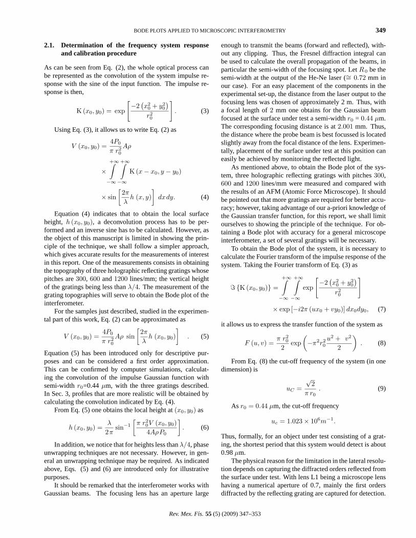
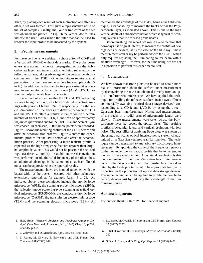
First, for each grating an average height distribution overthe small zone of interest was estimated. The three averages(one for each grating), obtained with the AFM, are shown inFig. 2a (Right). For each of these three average distributions,an rms vertical height value was obtained for each grating.
FIGURE 2. a). (Left) Line-profiles obtained with the interferometric technique. (Right) Line-profiles obtained with an atomic force micro-scope. b). Plot of the normalized frequency response of the system and the corresponding noise distribution.
Rev. Mex. Fıs. 55 (5) (2009) 347–353
BODE PLOTS APPLIED TO MICROSCOPIC INTERFEROMETRY 351
Second, for each grating an average height distributionwas obtained with the proposed technique, however, thistime, the resulting height distributions were obtained in voltsas expressed by Eq. (2). These measurements are shown onthe left side of Fig. 2a, already in nanometers as describedbellow.
In order to convert the Volts obtained for each gratinginto nanomemeters, we took in consideration the followingparameters:
i) the responsivity (ρ) of the photodetector, given in Am-peres/Watt
ii) the gain of the trans-impedance amplifier at the outputof the photodetector, and
iii) the power of the beam focused on the sample, whichcan be written asP0 = AdI0, whereAd is the areaof the photodiode andI0 the intensity of the beam, ac-cording to Eq. (6). Thus, we obtain directly the heightof the surface under test from the voltage measured bythe photodetector. This information is sent to a Lock-in amplifier and processed by a computer. The scan-ning distance is obtained by means of a previously cal-ibrated flexured piezoelectric (PZT).
Before proceeding with the experimental description, adiscussion on the results depicted in Fig. 2a is given. Adirect, detailed comparison between methods is not simple,as it is not possible to achieve exactly the same line scanwith both methods. In addition, the optical system is lim-ited in its lateral resolution because of diffraction; as usual,one can considerλg to be a limit. Further, the AFM respondsto different physical properties as compared with the opti-cal system. An ample discussion on this topic can be foundin Ref. 22. Figure 2a (Left) reveals that, the more difficultcase, the grating with a spatial frequency of1200 lines/mm(period = 0.83 µm), can easily be detected with the pro-posed method. Thus a lateral resolution nearλg is attained.This is attributed to the high vertical sensitivity of the systemthat in turn improves the lateral resolution. Thus, for a rea-sonable comparison of the methods, the average rms valuesof a set of measurements are used.
Third, from the above rms values obtained, the ratiosof the rms output voltages to the rms corresponding heightswere calculated for each spatial frequency.
A frequency response curve for the above ratios was fit-ted. For simplicity, a normalized plot is shown in Fig. 2b.It will be noticed that the frequency response experimentallyobtained is in good agreement with the theoretical responsegiven by Eq. (9).
As previously mentioned, the curve of the response wasadjusted by using only three points. This is done only for il-lustrative purposes and more points can be added if desired.For clarity, a symmetric spatial frequency axis is shown.
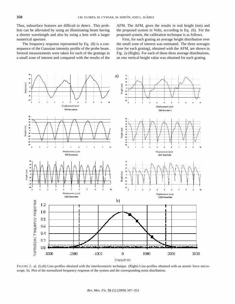
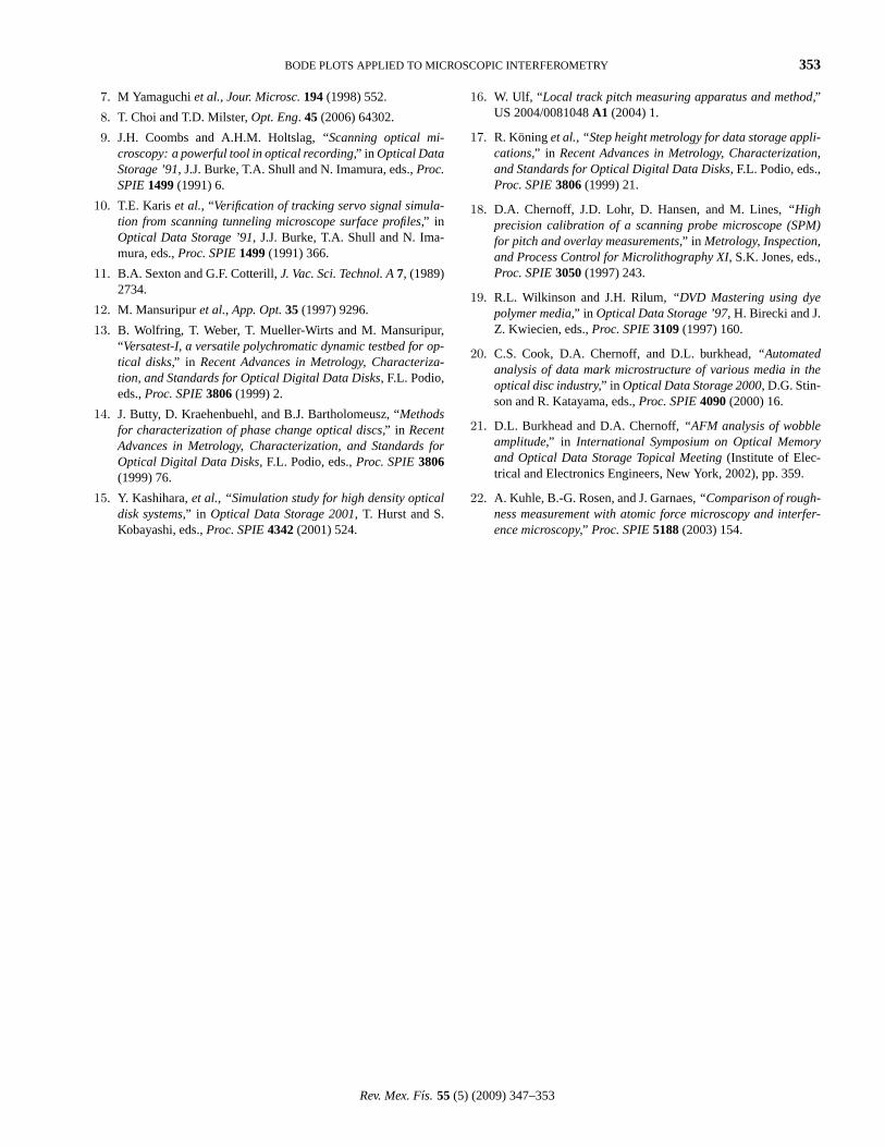
FIGURE 3. Line scans of a) CD-R and b) CD-R after the deconvo-lution process.
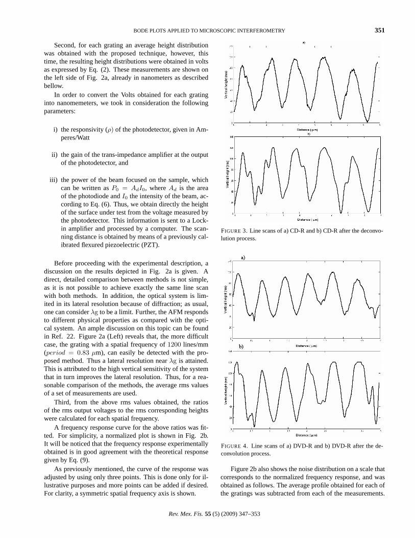
FIGURE 4. Line scans of a) DVD-R and b) DVD-R after the de-convolution process.
Figure 2b also shows the noise distribution on a scale thatcorresponds to the normalized frequency response, and wasobtained as follows. The average profile obtained for each ofthe gratings was subtracted from each of the measurements.
Rev. Mex. Fıs. 55 (5) (2009) 347–353
352 J.M. FLORES, M. CYWIAK, M. SERVIN, AND L. JUAREZ
Then, by placing each result of each subtraction one after an-other, a set was formed. This gives a representative noise ofthe set of samples. Finally, the Fourier transform of the setwas obtained and plotted. In Fig. 2b the vertical dotted linesindicate the useful area inside the filter that can be used torecover the input profile to be measured by the system.
3. Profile measurements
For the experiments, we arbitrarily chose a Sonyr CD-R anda Verbatimr DVD-R without data marks. The probe beamenters at a normal incidence, propagating across the Poly-carbonate layer, and travels back after being reflected by thereflective surface, taking advantage of the vertical depth dis-crimination of the (TGBI). Other techniques require specialpreparation for the measurements (see for example Refs. 5to 16). In addition, in the manufacture processing, it is com-mon to use an atomic force microscope (AFM) [17-21] be-fore the Polycarbonate layer is deposited.
It is important to mention that the CD and DVD reflectingsurfaces being measured, can be considered reflecting grat-ings with periods 1.6 and 0.74µm respectively. As the lat-eral dimensions of the tracks are different between the CDand the DVD, to attain a similar visualization of a certainnumber of tracks for the CD-R, a line scan of approximately10µm was performed and for the DVD-R, a line scan of 5µmwas chosen. In each scan, 1500 sample points were recorded.Figure 3 shows the resulting profiles of the CD-R before andafter the deconvolution process. Figure 4 shows the exper-imental profiles for the DVD before and after the deconvo-lution process. After processing, a more realistic profile isexpected as the high frequency features recover their origi-nal amplitude value. This would not be possible if one usedEqs. (5) directly. and (6). In adddition, the deconvolutionwas performed inside the valid frequency of the filter; thus,an additional advantage is that some noise has been filteredout as can be appreciated in the reported results.
The measurements shown are in good agreement with thelateral width of the tracks, measured with other techniquesextensively reported, as for example Refs. 5 to 21. Asindicated above, these techniques include the atomic forcemicroscope (AFM), the scanning probe microscope (SPM),the reflection-mode scattering-type scanning near-field op-tical microscope (RS-SNOM), the conductive-atomic forcemicroscope (C-AFM), the transmission electron microscope(TEM) and the scanning electron microscope (SEM). As
mentioned, the advantage of the TGBI, being a far field tech-nique, is its capability to measure the tracks across the Poly-carbonate layer, as indicated above. This is due to the highvertical depth of field discrimination which is typical of scan-ning systems that use focused probe beams.
Before finishing this report, we would like to mention thatnowadays it is of great interest, to measure the profiles of newhigh-density devices, as is the case of the blue ray. Thesemeasurements can easily be performed with the TGBI, whichonly requires replacing the illuminating source beam with asmaller wavelength. However, for the time being, we are notin a position to perform this experimental test.
4. Conclusions
We have shown that Bode plots can be used to obtain morerealistic information about the surface under measurementby deconvolving the raw data obtained directly from an op-tical inteferometric microscope. We have applied the tech-nique for profiling the reflected surfaces inside two differentcommercially available “optical data storage devices” cor-responding to a CD-R and DVD-R, by using the three -Gaussian- beam interferometer. Normalized measurementsof the tracks in a radial scan of micrometric length wereshown. These measurements were taken across the Poly-carbonate layer that covers the optical disks. The resultingprofiles showed high lateral and vertical resolution, with lownoise. The feasibility of applying Bode plots was shown bychoosing a particular optical interferometric system charac-terized by a Gaussian centered transfer function. The tech-nique can be generalized to any arbitrary microscopic inter-ferometer. By applying the curve of the frequency responseto the raw experimental data, a profile that better resemblesthe real surface was obtained. A collateral conclusion is thatthe combination of the three -Gaussian- beam interferome-ter with the deconvolution with the transfer function calcu-lated by the Bode plot turns out to be appropriate for qualityinspection in the production of optical data storage devices.The same technique can be applied to profile the new high-density devices just by reducing the wavelength of the illu-minating source.
Acknowledgments
The authors thank CONACYT for financial support.
1. H.W. Bode, “Network Analysis and Feedback Amplifier De-sign” (Van Nostrand, Princeton, N.J., 1945) Chap.13, p.286;Chap.15, p.337.
2. Z. Zalevsky and D. Mendlovic,Appl. Opt.34 (1995) 828.
3. L. Juarez, M. Cywiak, B. Barrientos, and J.M. Flores,Opt.Commun.268(2006) 209.
4. L. Juarez, M. Cywiak, M. Servın, and J.M. Flores,Opt. Express15 (2007) 5277.
5. T. Kikukawa and H. Utsunomiya,Microsc. Microanal.7 (2001)363.
6. S. Kai, I. Chun, and D. Ping,Opt. Express14 (2006) 4452.
Rev. Mex. Fıs. 55 (5) (2009) 347–353
BODE PLOTS APPLIED TO MICROSCOPIC INTERFEROMETRY 353
7. M Yamaguchiet al., Jour. Microsc.194(1998) 552.
8. T. Choi and T.D. Milster,Opt. Eng. 45 (2006) 64302.
9. J.H. Coombs and A.H.M. Holtslag, “Scanning optical mi-croscopy: a powerful tool in optical recording,” in Optical DataStorage ’91, J.J. Burke, T.A. Shull and N. Imamura, eds.,Proc.SPIE1499(1991) 6.
10. T.E. Kariset al., “Verification of tracking servo signal simula-tion from scanning tunneling microscope surface profiles,” inOptical Data Storage ’91, J.J. Burke, T.A. Shull and N. Ima-mura, eds.,Proc. SPIE1499(1991) 366.
11. B.A. Sexton and G.F. Cotterill,J. Vac. Sci. Technol. A7, (1989)2734.
12. M. Mansuripuret al., App. Opt.35 (1997) 9296.
13. B. Wolfring, T. Weber, T. Mueller-Wirts and M. Mansuripur,“Versatest-I, a versatile polychromatic dynamic testbed for op-tical disks,” in Recent Advances in Metrology, Characteriza-tion, and Standards for Optical Digital Data Disks, F.L. Podio,eds.,Proc. SPIE3806(1999) 2.
14. J. Butty, D. Kraehenbuehl, and B.J. Bartholomeusz, “Methodsfor characterization of phase change optical discs,” in RecentAdvances in Metrology, Characterization, and Standards forOptical Digital Data Disks, F.L. Podio, eds.,Proc. SPIE3806(1999) 76.
15. Y. Kashihara,et al., “Simulation study for high density opticaldisk systems,”in Optical Data Storage 2001, T. Hurst and S.Kobayashi, eds.,Proc. SPIE4342(2001) 524.
16. W. Ulf, “ Local track pitch measuring apparatus and method,”US 2004/0081048A1 (2004) 1.
17. R. Koninget al., “Step height metrology for data storage appli-cations,” in Recent Advances in Metrology, Characterization,and Standards for Optical Digital Data Disks, F.L. Podio, eds.,Proc. SPIE3806(1999) 21.
18. D.A. Chernoff, J.D. Lohr, D. Hansen, and M. Lines,“Highprecision calibration of a scanning probe microscope (SPM)for pitch and overlay measurements,”in Metrology, Inspection,and Process Control for Microlithography XI, S.K. Jones, eds.,Proc. SPIE3050(1997) 243.
19. R.L. Wilkinson and J.H. Rilum,“DVD Mastering using dyepolymer media,”in Optical Data Storage ’97, H. Birecki and J.Z. Kwiecien, eds.,Proc. SPIE3109(1997) 160.
20. C.S. Cook, D.A. Chernoff, and D.L. burkhead,“Automatedanalysis of data mark microstructure of various media in theoptical disc industry,”in Optical Data Storage 2000, D.G. Stin-son and R. Katayama, eds.,Proc. SPIE4090(2000) 16.
21. D.L. Burkhead and D.A. Chernoff,“AFM analysis of wobbleamplitude,” in International Symposium on Optical Memoryand Optical Data Storage Topical Meeting(Institute of Elec-trical and Electronics Engineers, New York, 2002), pp. 359.
22. A. Kuhle, B.-G. Rosen, and J. Garnaes,“Comparison of rough-ness measurement with atomic force microscopy and interfer-ence microscopy,” Proc. SPIE5188(2003) 154.
Rev. Mex. Fıs. 55 (5) (2009) 347–353


![Prof. Dr. S. Zacher Stabilitätsprüfung und Regler ... · Das Zwei-Bode-Plots Verfahren wurde von Zacher aus dem Zweiortskurvenverfahren [1] hergeleitet und zu einem neuen Stabilitätskriterium](https://img.pdfslide.tips/doc/110x75/5e146a3f741ea236bf78183a/prof-dr-s-zacher-stabilittsprfung-und-regler-das-zwei-bode-plots-verfahren.jpg)