Embed Size (px)
Citation preview
8/8/2019 Boost Convertor
http://slidepdf.com/reader/full/boost-convertor 1/28
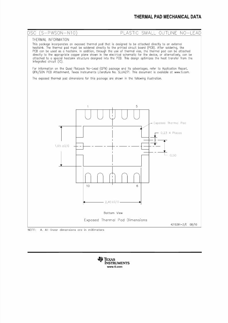
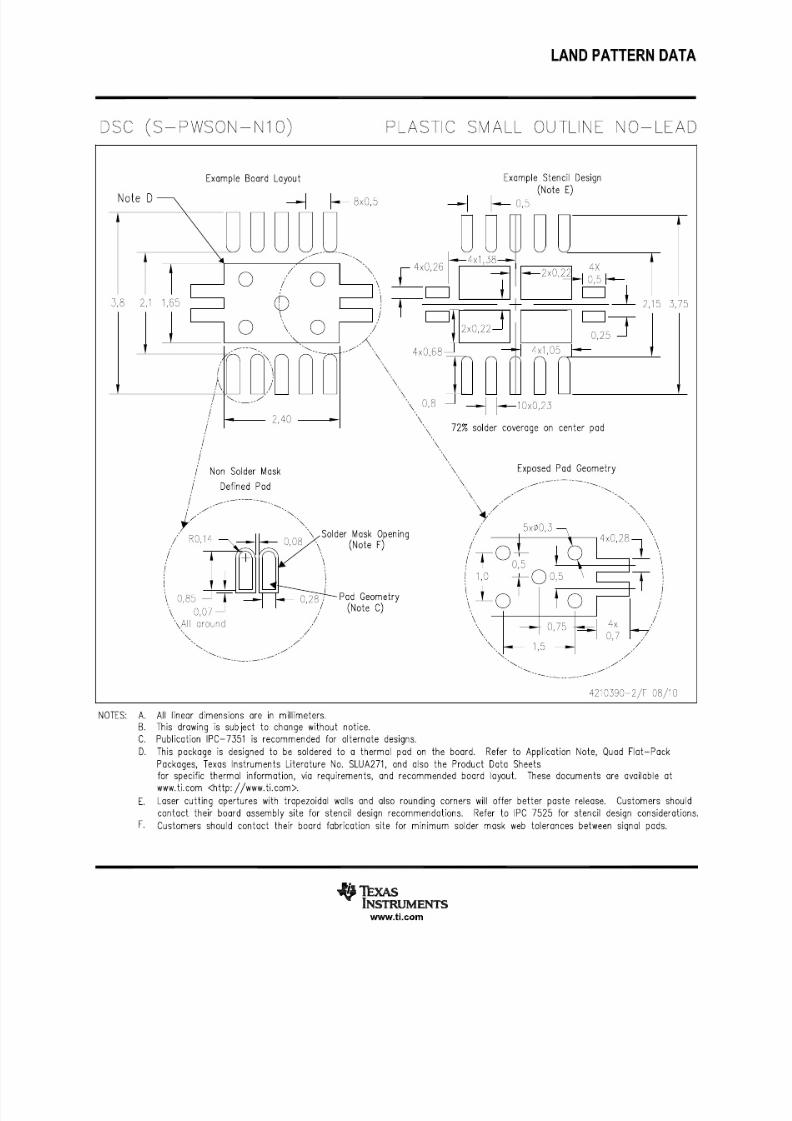
Actual Size
3 mm x 3 mm
IN
EN
SW
FBFREQ
AGND COMP
SS
14
68
3 7
2
5PGND
9
10
SW
Cby
1 F
16V
m
Cin2*10 F16Vm
V
2.5Vto6VIN
L
3.3 Hm
DSL22
V
15V/500mAS
R1200kW
R2
18kW
Cout
4*10 F25V
m
Rcomp
100kW
Ccomp820pFCss
100nFTPS61087
TP S 61 08 7
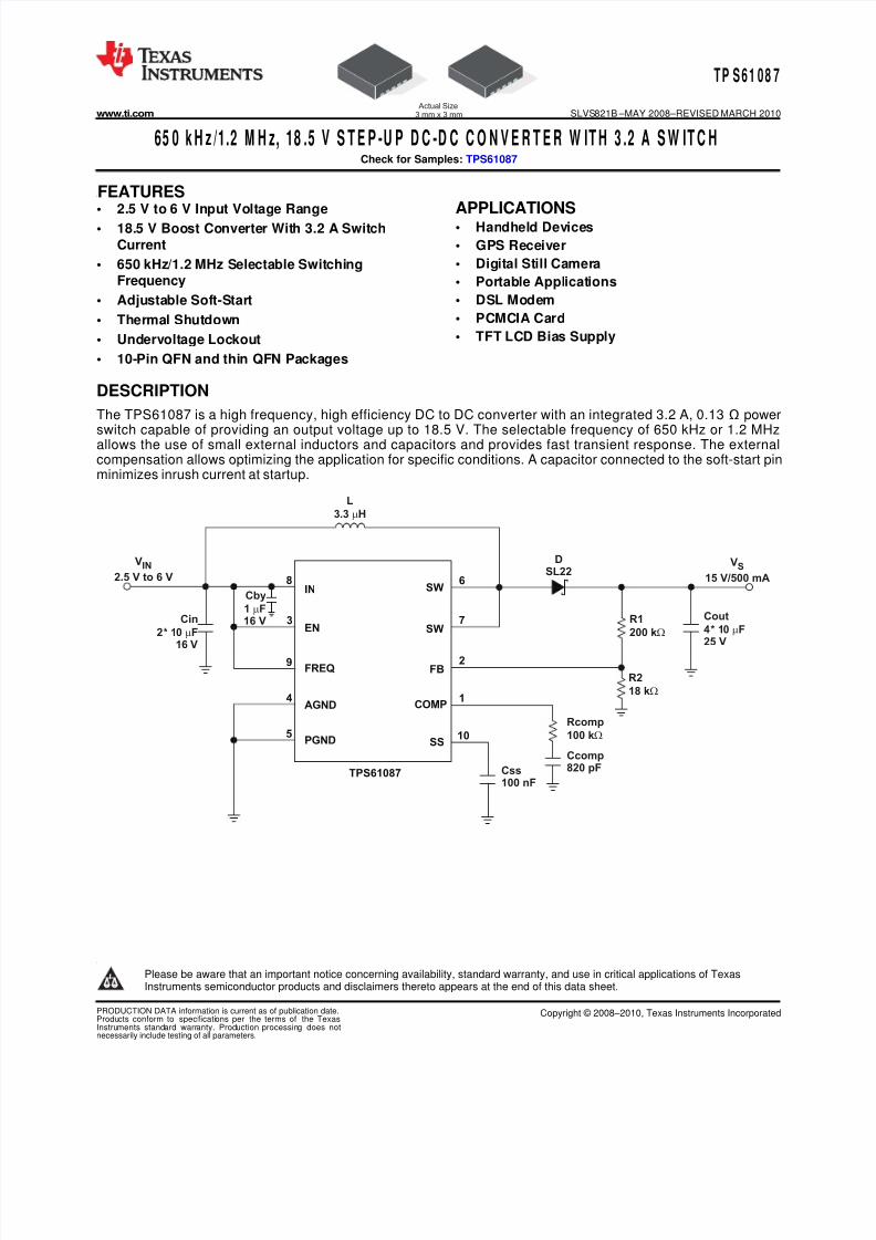
www.ti.com SLVS821B –MAY 2008–REVISED MARCH 2010
65 0 k H z /1.2 M H z, 18 .5 V S T E P -U P D C -D C C O N V E R T E R W IT H 3 .2 A S W IT C HCheck for Samples: TPS61087
1FEATURES
• 2.5 V to 6 V Input Voltage Range APPLICATIONS• Handheld Devices• 18.5 V Boost Converter With 3.2 A Switch
Current • GPS Receiver
• Digital Still Camera• 650 kHz/1.2 MHz Selectable SwitchingFrequency • Portable Applications
• DSL Modem• Adjustable Soft-Start
• PCMCIA Card• Thermal Shutdown
• TFT LCD Bias Supply• Undervoltage Lockout
• 10-Pin QFN and thin QFN Packages
DESCRIPTION
The TPS61087 is a high frequency, high efficiency DC to DC converter with an integrated 3.2 A, 0.13 Ω powerswitch capable of providing an output voltage up to 18.5 V. The selectable frequency of 650 kHz or 1.2 MHzallows the use of small external inductors and capacitors and provides fast transient response. The externalcompensation allows optimizing the application for specific conditions. A capacitor connected to the soft-start pinminimizes inrush current at startup.
1
Please be aware that an important notice concerning availability, standard warranty, and use in critical applications of TexasInstruments semiconductor products and disclaimers thereto appears at the end of this data sheet.
PRODUCTION DATA information is current as of publication date. Copyright © 2008–2010, Texas Instruments IncorporatedProducts conform to specifications per the terms of the TexasInstruments standard warranty. Production processing does not
necessarily include testing of all parameters.
8/8/2019 Boost Convertor
http://slidepdf.com/reader/full/boost-convertor 2/28
TP S 61 08 7
SLVS821B –MAY 2008–REVISED MARCH 2010 www.ti.com
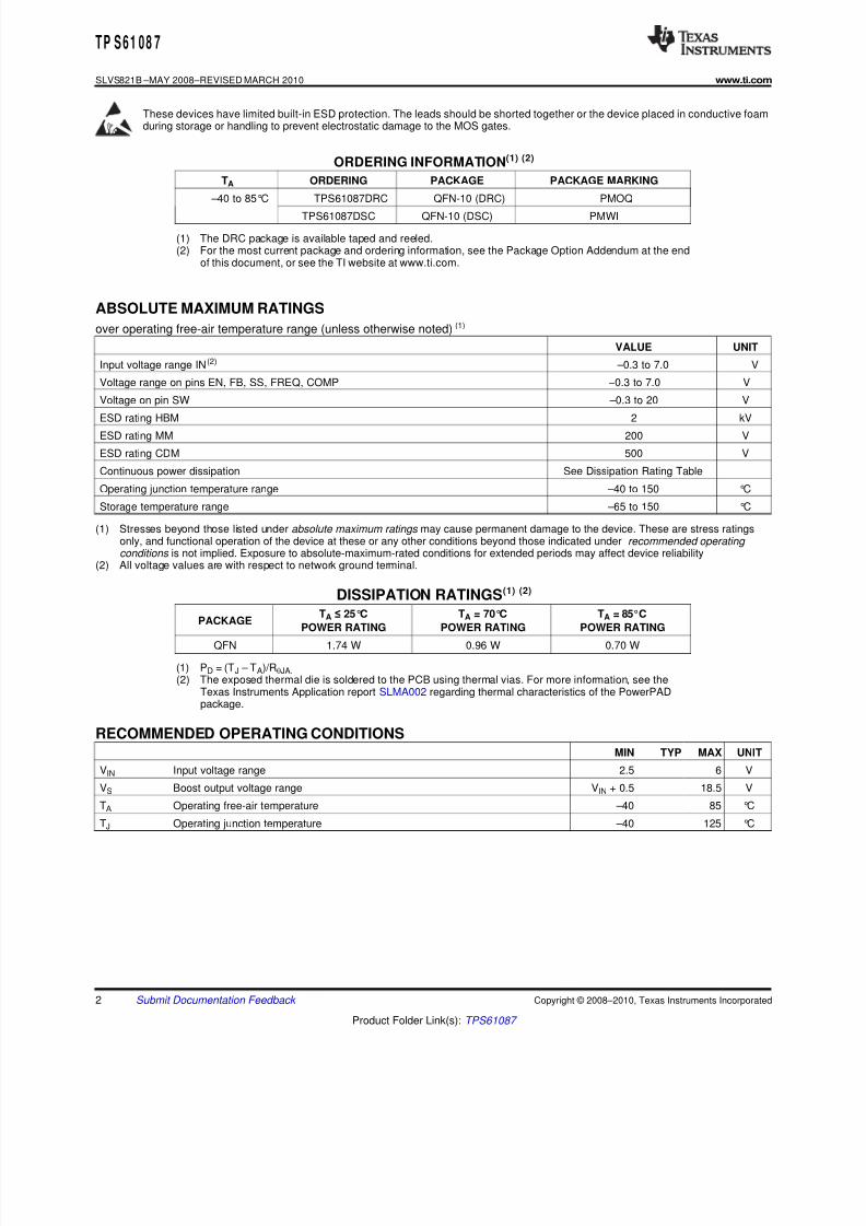
These devices have limited built-in ESD protection. The leads should be shorted together or the device placed in conductive foamduring storage or handling to prevent electrostatic damage to the MOS gates.
ORDERING INFORMATION(1) (2)
TA ORDERING PACKAGE PACKAGE MARKING
–40 to 85°C TPS61087DRC QFN-10 (DRC) PMOQ
TPS61087DSC QFN-10 (DSC) PMWI
(1) The DRC package is available taped and reeled.(2) For the most current package and ordering information, see the Package Option Addendum at the end
of this document, or see the TI website at www.ti.com.
ABSOLUTE MAXIMUM RATINGS
over operating free-air temperature range (unless otherwise noted) (1)
VALUE UNIT
Input voltage range IN (2) –0.3 to 7.0 V
Voltage range on pins EN, FB, SS, FREQ, COMP –0.3 to 7.0 V
Voltage on pin SW –0.3 to 20 V
ESD rating HBM 2 kV
ESD rating MM 200 V
ESD rating CDM 500 V
Continuous power dissipation See Dissipation Rating Table
Operating junction temperature range –40 to 150 °C
Storage temperature range –65 to 150 °C
(1) Stresses beyond those listed under absolute maximum ratings may cause permanent damage to the device. These are stress ratingsonly, and functional operation of the device at these or any other conditions beyond those indicated under recommended operating conditions is not implied. Exposure to absolute-maximum-rated conditions for extended periods may affect device reliability
(2) All voltage values are with respect to network ground terminal.
DISSIPATION RATINGS(1) (2)
TA ≤ 25°C TA = 70°C TA = 85°CPACKAGEPOWER RATING POWER RATING POWER RATING
QFN 1.74 W 0.96 W 0.70 W
(1) PD = (TJ – TA)/RqJA.
(2) The exposed thermal die is soldered to the PCB using thermal vias. For more information, see theTexas Instruments Application report SLMA002 regarding thermal characteristics of the PowerPADpackage.
RECOMMENDED OPERATING CONDITIONSMIN TYP MAX UNIT
VIN Input voltage range 2.5 6 V
VS Boost output voltage range VIN + 0.5 18.5 V
TA Operating free-air temperature –40 85 °C
TJ Operating junction temperature –40 125 °C
2 Submit Documentation Feedback Copyright © 2008–2010, Texas Instruments Incorporated
Product Folder Link(s): TPS61087
8/8/2019 Boost Convertor
http://slidepdf.com/reader/full/boost-convertor 3/28
TP S 61 08 7
www.ti.com SLVS821B –MAY 2008–REVISED MARCH 2010
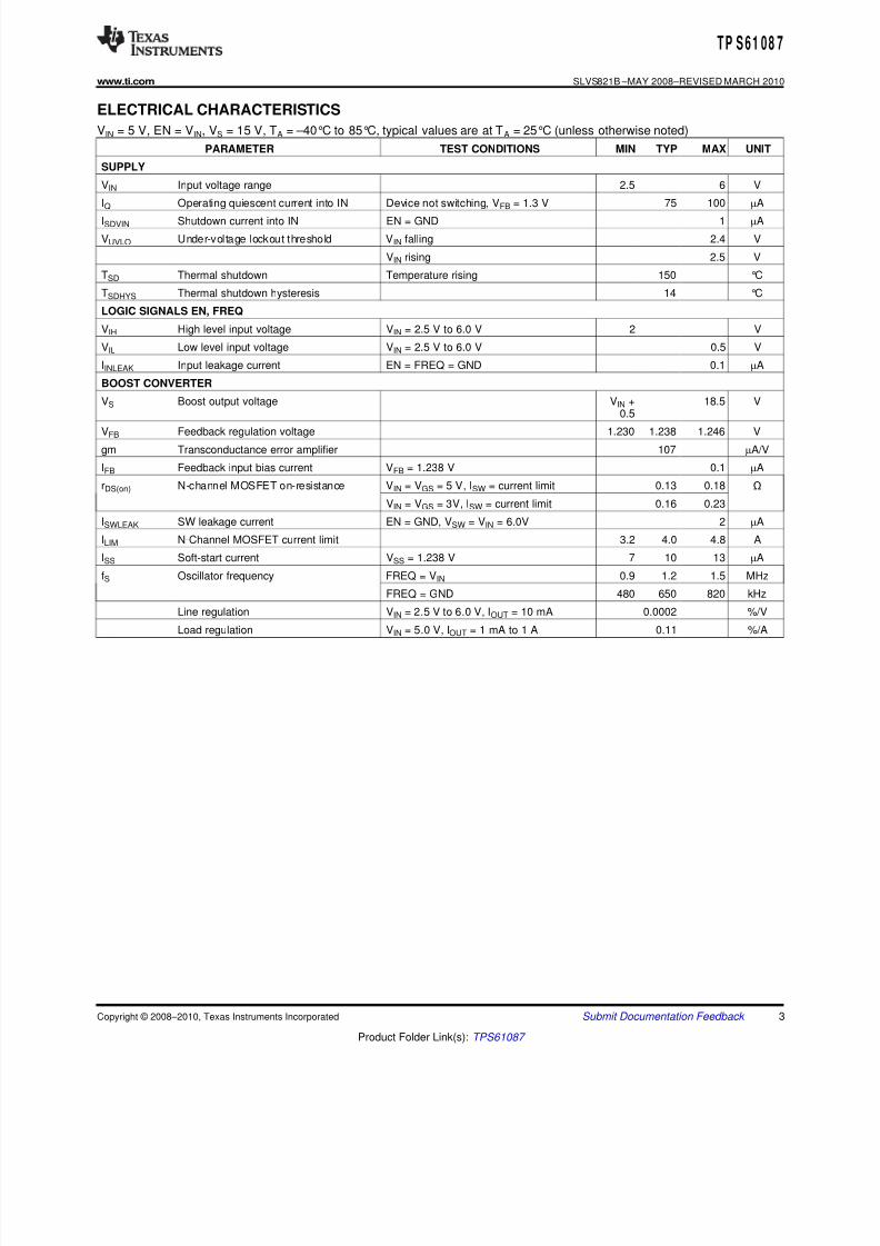
ELECTRICAL CHARACTERISTICS
VIN = 5 V, EN = VIN, VS = 15 V, TA = –40°C to 85°C, typical values are at TA = 25°C (unless otherwise noted)
PARAMETER TEST CONDITIONS MIN TYP MAX UNIT
SUPPLY
VIN Input voltage range 2.5 6 V
IQ Operating quiescent current into IN Device not switching, VFB = 1.3 V 75 100 mAISDVIN Shutdown current into IN EN = GND 1 mA
VUVLO Under-voltage lockout threshold VIN falling 2.4 V
VIN rising 2.5 V
TSD Thermal shutdown Temperature rising 150 °C
TSDHYS Thermal shutdown hysteresis 14 °C
LOGIC SIGNALS EN, FREQ
VIH High level input voltage VIN = 2.5 V to 6.0 V 2 V
VIL Low level input voltage VIN = 2.5 V to 6.0 V 0.5 V
IINLEAK Input leakage current EN = FREQ = GND 0.1 mA
BOOST CONVERTER
VS Boost output voltage VIN + 18.5 V
0.5VFB Feedback regulation voltage 1.230 1.238 1.246 V
gm Transconductance error amplifier 107 mA/V
IFB Feedback input bias current VFB = 1.238 V 0.1 mA
rDS(on) N-channel MOSFET on-resistance VIN = VGS = 5 V, ISW = current limit 0.13 0.18 Ω
VIN = VGS = 3V, ISW = current limit 0.16 0.23
ISWLEAK SW leakage current EN = GND, VSW = VIN = 6.0V 2 mA
ILIM N-Channel MOSFET current limit 3.2 4.0 4.8 A
ISS Soft-start current VSS = 1.238 V 7 10 13 mA
fS Oscillator frequency FREQ = VIN 0.9 1.2 1.5 MHz
FREQ = GND 480 650 820 kHz
Line regulation VIN = 2.5 V to 6.0 V, IOUT = 10 mA 0.0002 %/V
Load regulation VIN = 5.0 V, IOUT = 1 mA to 1 A 0.11 %/A
Copyright © 2008–2010, Texas Instruments Incorporated Submit Documentation Feedback 3
Product Folder Link(s): TPS61087
8/8/2019 Boost Convertor
http://slidepdf.com/reader/full/boost-convertor 4/28
SW
SS
FREQ
IN
SW
AGND
COMP
FB
EN
PGND
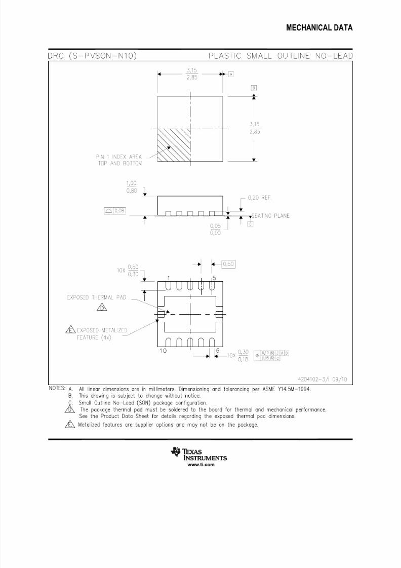
10-PIN3mmx3mmx1mmQFN
ThermalPad
TP S 61 08 7
SLVS821B –MAY 2008–REVISED MARCH 2010 www.ti.com
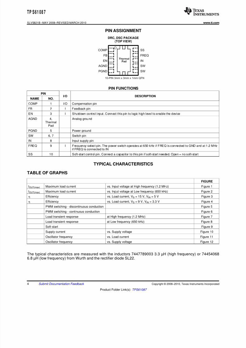
PIN ASSIGNMENT
DRC, DSC PACKAGE(TOP VIEW)
PIN FUNCTIONS
PINI/O DESCRIPTION
NAME NO.
COMP 1 I/O Compensation pin
FB 2 I Feedback pin
EN 3 I Shutdown control input. Connect this pin to logic high level to enable the device
AGND 4, Analog groundThermal
Pad
PGND 5 Power ground
SW 6, 7 Switch pin
IN 8 Input supply pin
FREQ 9 I Frequency select pin. The power switch operates at 650 kHz if FREQ is connected to GND and at 1.2 MHzif FREQ is connected to IN
SS 10 Soft-start control pin. Connect a capacitor to this pin if soft-start needed. Open = no soft-start
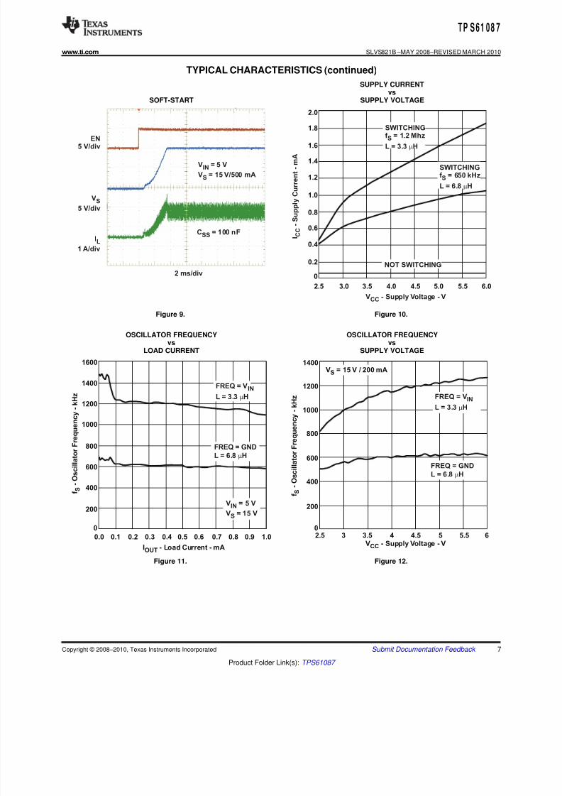
TYPICAL CHARACTERISTICS
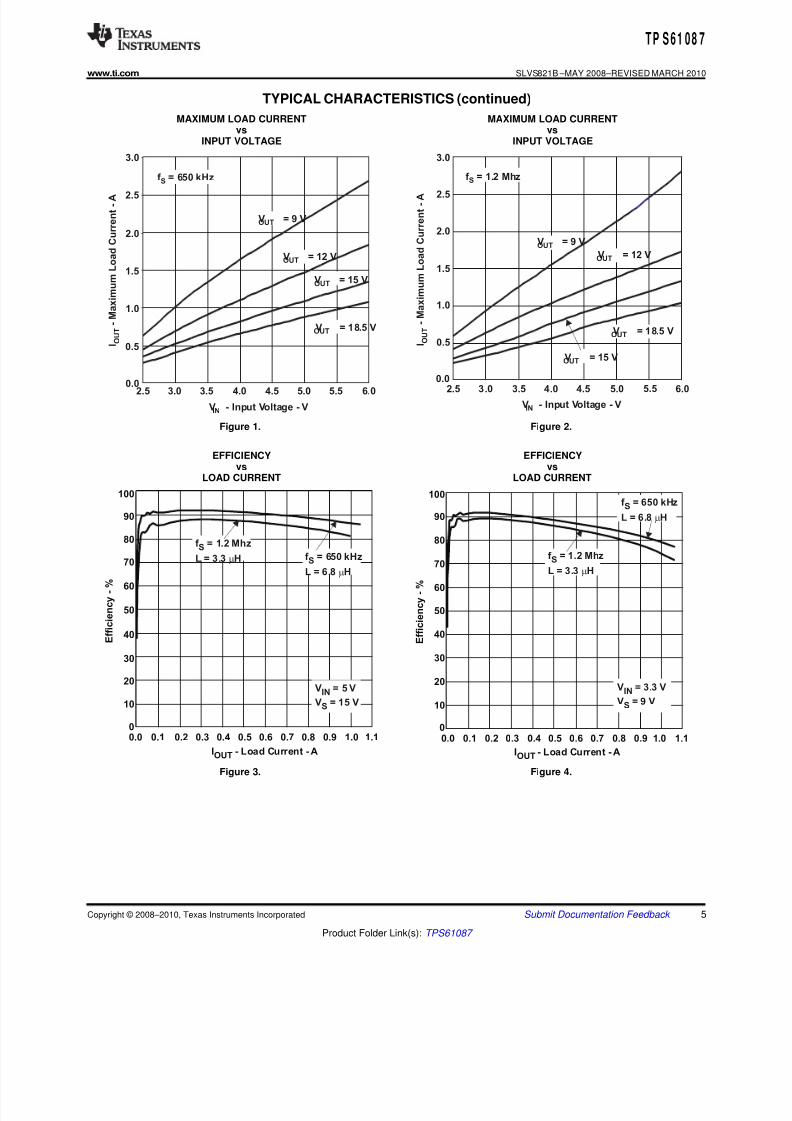
TABLE OF GRAPHSFIGURE
IOUT(max) Maximum load current vs. Input voltage at High frequency (1.2 MHz) Figure 1
IOUT(max) Maximum load current vs. Input voltage at Low frequency (650 kHz) Figure 2
h Efficiency vs. Load current, VS = 15 V, VIN = 5 V Figure 3
h Efficiency vs. Load current, VS = 9 V, VIN = 3.3 V Figure 4
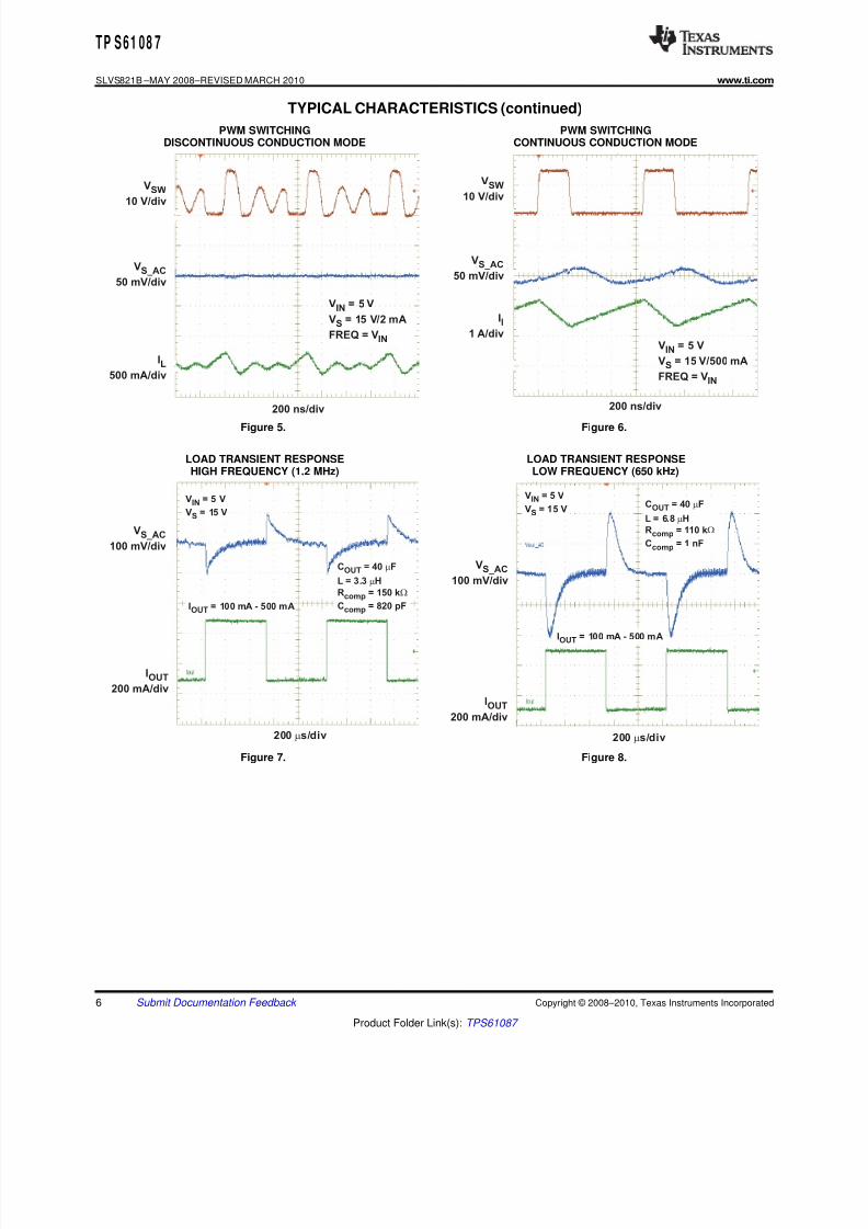
PWM switching - discontinuous conduction Figure 5
PWM switching - continuous conduction Figure 6
Load transient response at High frequency (1.2 MHz) Figure 7
Load transient response at Low frequency (650 kHz) Figure 8
Soft-start Figure 9
Supply current vs. Supply voltage Figure 10Oscillator frequency vs. Load current Figure 11
Oscillator frequency vs. Supply voltage Figure 12
The typical characteristics are measured with the inductors 7447789003 3.3 µH (high frequency) or 744540686.8 µH (low frequency) from Wurth and the rectifier diode SL22.
4 Submit Documentation Feedback Copyright © 2008–2010, Texas Instruments Incorporated
Product Folder Link(s): TPS61087
8/8/2019 Boost Convertor
http://slidepdf.com/reader/full/boost-convertor 5/28
V -InputVoltage-VIN
I
- M a x
i m u m
L o a
d C u r r e n
t -
A
O U T
3.0
2.5
2.0
1.5
1.0
0.5
0.04.52.5 3.0 3.5 4.0 5.0 5.5 6.0
V =9VOUT
V =15VOUT
V =18.5VOUT
f =1.2MhzS
V =12VOUT
V =9VOUT
V =12VOUT
V =15VOUT
V =18.5VOUT
V -InputVoltage-VIN
I
- M a x
i m u m
L o a
d C u r r e n
t -
A
O U T
3.0
2.5
2.0
1.5
1.0
0.5
0.02.5 3.0 3.5 4.0 4.5 5.0 5.5 6.0
f =650kHzS
0
10
20
30
40
50
60
70
80
90
100
0.0 0.1 0.2 0.3 0.4 0.5 0.6 0.7 0.8 0.9 1.0 1.1
I -LoadCurrent- AOUT
E f f i c i e n c y
- %
f =650kHz
L =6.8 HS
m
f =1.2Mhz
L =3.3 H
S
m
V = 5V
V =15V
IN
S
0
10
20
30
40
50
60
70
80
90
100
0.0 0.1 0.2 0.3 0.4 0.5 0.6 0.7 0.8 0.9 1.0 1.1
I -LoadCurrent- AOUT
E f f i c i e n c y
- %
f =650kHz
L =6.8 H
S
m
f =1.2Mhz
L =3.3 H
S
m
V =3.3V
V =9V
IN
S
TP S 61 08 7
www.ti.com SLVS821B –MAY 2008–REVISED MARCH 2010
TYPICAL CHARACTERISTICS (continued)
MAXIMUM LOAD CURRENT MAXIMUM LOAD CURRENTvs vs
INPUT VOLTAGE INPUT VOLTAGE
Figure 1. Figure 2.
EFFICIENCY EFFICIENCYvs vs
LOAD CURRENT LOAD CURRENT
Figure 3. Figure 4.
Copyright © 2008–2010, Texas Instruments Incorporated Submit Documentation Feedback 5
Product Folder Link(s): TPS61087
8/8/2019 Boost Convertor
http://slidepdf.com/reader/full/boost-convertor 6/28
V
10V/divSW
V
50mV/divS_AC
I
1 A/divl
200ns/div
V =5V
V =15V/500mA
FREQ=V
IN
S
IN
V
10V/div
SW
V
50mV/divS_AC
I
500mA/divL
200ns/div
V = 5V
V =15V/2mA
FREQ=V
IN
S
IN
V
100mV/divS_AC
I
200mA/divOUT
200 s/divm
V =5V
V =15VIN
S
I =100mA -500mAOUT
C =40 F
L =3.3 H
R =150k
C =820pF
OUT
comp
comp
m
m
W
V
100mV/divS_AC
I
200mA/divOUT
V =5 V
V =15VIN
S
I =100mA -500mAOUT
C =40 F
L =6.8 H
R =110k
C =1nF
OUT
comp
comp
m
m
W
200 s/divm
TP S 61 08 7
SLVS821B –MAY 2008–REVISED MARCH 2010 www.ti.com
TYPICAL CHARACTERISTICS (continued)
PWM SWITCHING PWM SWITCHINGDISCONTINUOUS CONDUCTION MODE CONTINUOUS CONDUCTION MODE
Figure 5. Figure 6.
LOAD TRANSIENT RESPONSE LOAD TRANSIENT RESPONSEHIGH FREQUENCY (1.2 MHz) LOW FREQUENCY (650 kHz)
Figure 7. Figure 8.
6 Submit Documentation Feedback Copyright © 2008–2010, Texas Instruments Incorporated
Product Folder Link(s): TPS61087
8/8/2019 Boost Convertor
http://slidepdf.com/reader/full/boost-convertor 7/28
EN
5V/div
V
5V/div
S
I
1 A/div
L
V =5 V
V =15V/500mA
IN
S
C =100nFSS
2ms/div 0
0.2
0.4
0.6
0.8
1.0
1.2
1.4
1.6
1.8
2.0
2.5 3.0 3.5 4.0 4.5 5.0 5.5 6.0
SWITCHINGf =1.2Mhz
L =3.3 H
S
m
SWITCHINGf =650kHz
L =6.8 H
S
m
NOTSWITCHING
I
- S u p p
l y C u r r e n
t -
m A
C C
V -SupplyVoltage-VCC
0
200
400
600
800
1000
1200
1400
1600
0.0 0.1 0.2 0.3 0.4 0.5 0.6 0.7 0.8 0.9 1.0
I -LoadCurrent-mAOUT
f
- O s c
i l l a t o r
F r e q u e n c y -
k H
z
S
FREQ=V
L =3.3 H
IN
m
FREQ=GND
L =6.8 Hm
V = 5 V
V =15V
IN
S
0
200
400
600
800
1000
1200
1400
2.5 3 3.5 4 4.5 5 5.5 6V -SupplyVoltage-VCC
f
- O s c
i l l a t o r
F r e q u e n c y -
k H z
S
V =15V/200mAS
FREQ=VL =3.3 H
INm
FREQ=GND
L =6.8 Hm
TP S 61 08 7
www.ti.com SLVS821B –MAY 2008–REVISED MARCH 2010
TYPICAL CHARACTERISTICS (continued)
SUPPLY CURRENTvs
SOFT-START SUPPLY VOLTAGE
Figure 9. Figure 10.
OSCILLATOR FREQUENCY OSCILLATOR FREQUENCYvs vs
LOAD CURRENT SUPPLY VOLTAGE
Figure 11. Figure 12.
Copyright © 2008–2010, Texas Instruments Incorporated Submit Documentation Feedback 7
Product Folder Link(s): TPS61087
8/8/2019 Boost Convertor
http://slidepdf.com/reader/full/boost-convertor 8/28
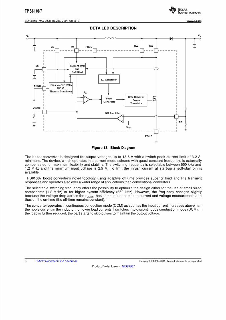
COMP
FB
GM Amplifier
Vref
SW SW
GateDriverof
Power
Transistor
IN
SS
PWM
Generator
Currentlimit
and
SoftStart
t Generator OFF
tON
PGND
BiasVref = 1.238V
UVLO
ThermalShutdown
AGND
EN FREQ
VIN VS
TP S 61 08 7
SLVS821B –MAY 2008–REVISED MARCH 2010 www.ti.com
DETAILED DESCRIPTION
Figure 13. Block Diagram
The boost converter is designed for output voltages up to 18.5 V with a switch peak current limit of 3.2 A
minimum. The device, which operates in a current mode scheme with quasi-constant frequency, is externallycompensated for maximum flexibility and stability. The switching frequency is selectable between 650 kHz and1.2 MHz and the minimum input voltage is 2.5 V. To limit the inrush current at start-up a soft-start pin isavailable.
TPS61087 boost converter’s novel topology using adaptive off-time provides superior load and line transientresponses and operates also over a wider range of applications than conventional converters.
The selectable switching frequency offers the possibility to optimize the design either for the use of small sizedcomponents (1.2 MHz) or for higher system efficiency (650 kHz). However, the frequency changes slightlybecause the voltage drop across the rDS(on) has some influence on the current and voltage measurement andthus on the on-time (the off-time remains constant).
The converter operates in continuous conduction mode (CCM) as soon as the input current increases above halfthe ripple current in the inductor, for lower load currents it switches into discontinuous conduction mode (DCM). If
the load is further reduced, the part starts to skip pulses to maintain the output voltage.
8 Submit Documentation Feedback Copyright © 2008–2010, Texas Instruments Incorporated
Product Folder Link(s): TPS61087

8/8/2019 Boost Convertor
http://slidepdf.com/reader/full/boost-convertor 9/28
1IN
S
V D
V
h×= -
( )(max) (min) 12
L
out LIM
I I I D
Dæ ö= - × -ç ÷
è ø
D
I I I out L swpeak
-+
D=
12
IN L
S
V D I
f L
×D =
×
TP S 61 08 7
www.ti.com SLVS821B –MAY 2008–REVISED MARCH 2010
Design Procedure
The first step in the design procedure is to verify that the maximum possible output current of the boost convertersupports the specific application requirements. A simple approach is to estimate the converter efficiency, bytaking the efficiency numbers from the provided efficiency curves or to use a worst case assumption for theexpected efficiency, e.g. 90%.
1. Duty cycle, D :
(1)
2. Maximum output current, I out(max) :
(2)
3. Peak switch current in application, I swpeak :
(3)
with the inductor peak-to-peak ripple current, ΔI L
(4)
and
V IN Minimum input voltage
V S Output voltage
I LIM(min) Converter switch current limit (minimum switch current limit = 3.2 A)
f S Converter switching frequency (typically 1.2 MHz or 650 kHz)
L Selected inductor value
h Estimated converter efficiency (please use the number from the efficiency plots or 90% as an estimation)
The peak switch current is the steady state peak switch current that the integrated switch, inductor and externalSchottky diode has to be able to handle. The calculation must be done for the minimum input voltage where thepeak switch current is the highest.
Soft-start
The boost converter has an adjustable soft-start to prevent high inrush current during start-up. To minimize theinrush current during start-up an external capacitor, connected to the soft-start pin SS and charged with aconstant current, is used to slowly ramp up the internal current limit of the boost converter. When the EN pin ispulled high, the soft-start capacitor CSS is immediately charged to 0.3 V. The capacitor is then charged at aconstant current of 10 mA typically until the output of the boost converter VS has reached its Power Goodthreshold (roughly 98% of VS nominal value). During this time, the SS voltage directly controls the peak inductorcurrent, starting with 0 A at VSS = 0.3 V up to the full current limit at VSS = 800 mV. The maximum load current is
available after the soft-start is completed. The larger the capacitor the slower the ramp of the current limit and thelonger the soft-start time. A 100 nF capacitor is usually sufficient for most of the applications. When the EN pin ispulled low, the soft-start capacitor is discharged to ground.
Copyright © 2008–2010, Texas Instruments Incorporated Submit Documentation Feedback 9
Product Folder Link(s): TPS61087

8/8/2019 Boost Convertor
http://slidepdf.com/reader/full/boost-convertor 10/28
2
-
0.35
IN S IN
S out S
V V V L
V I f
hæ öæ ö æ ö= × ×ç ÷ç ÷ ç ÷× è øè ø è ø
TP S 61 08 7
SLVS821B –MAY 2008–REVISED MARCH 2010 www.ti.com
Inductor Selection
The TPS61087 is designed to work with a wide range of inductors. The main parameter for the inductor selectionis the saturation current of the inductor which should be higher than the peak switch current as calculated in theDesign Procedure section with additional margin to cover for heavy load transients. An alternative, moreconservative, is to choose an inductor with a saturation current at least as high as the maximum switch currentlimit of 4.8 A. The other important parameter is the inductor DC resistance. Usually the lower the DC resistance
the higher the efficiency. It is important to note that the inductor DC resistance is not the only parameterdetermining the efficiency. Especially for a boost converter where the inductor is the energy storage element, thetype and core material of the inductor influences the efficiency as well. At high switching frequencies of 1.2 MHzinductor core losses, proximity effects and skin effects become more important. Usually an inductor with a largerform factor gives higher efficiency. The efficiency difference between different inductors can vary between 2% to10%. For the TPS61087, inductor values between 3 mH and 6 mH are a good choice with a switching frequencyof 1.2 MHz, typically 3.3 mH. At 650 kHz we recommend inductors between 6 mH and 13 mH, typically 6.8 mH.Possible inductors are shown in Table 1.
Typically, it is recommended that the inductor current ripple is below 35% of the average inductor current.Therefore, the following equation can be used to calculate the inductor value, L:
(5)with
V IN Minimum input voltage
V S Output voltage
I out Maximum output current in the application
f S Converter switching frequency (typically 1.2 MHz or 650 kHz)
h Estimated converter efficiency (please use the number from the efficiency plots or 90% as an estimation)
Table 1. Inductor Selection
L COMPONENT SIZE DCR TYPSUPPLIER Isat (A)CODE(mH) (L×W×H mm) (mΩ)
1.2 MHz
4.2 Sumida CDRH5D28 5.7 × 5.7 × 3 23 2.2
4.7 Wurth Elektronik 7447785004 5.9 × 6.2 × 3.3 60 2.5
5 Coilcraft MSS7341 7.3 × 7.3 × 4.1 24 2.9
5 Sumida CDRH6D28 7 × 7 × 3 23 2.4
4.6 Sumida CDR7D28 7.6 × 7.6 × 3 38 3.15
4.7 Wurth Elektronik 7447789004 7.3 × 7.3 × 3.2 33 3.9
3.3 Wurth Elektronik 7447789003 7.3 × 7.3 × 3.2 30 4.2
650 kHz
10 Wurth Elektronik 744778910 7.3 × 7.3 × 3.2 51 2.2
10 Sumida CDRH8D28 8.3 × 8.3 × 3 36 2.7
6.8 Sumida CDRH6D26HPNP 7 × 7 × 2.8 52 2.9
6.2 Sumida CDRH8D58 8.3 × 8.3 × 6 25 3.3
10 Coilcraft DS3316P 12.95 × 9.40 × 80 3.55.08
10 Sumida CDRH8D43 8.3 × 8.3 × 4.5 29 4
6.8 Wurth Elektronik 74454068 12.7 × 10 × 4.9 55 4.1
10 Submit Documentation Feedback Copyright © 2008–2010, Texas Instruments Incorporated
Product Folder Link(s): TPS61087
8/8/2019 Boost Convertor
http://slidepdf.com/reader/full/boost-convertor 11/28
avg out I I =
D avg forward P I V = ×
2 1870
1.238
m= » W
=
FB
FB
V R k
A
V V
1 2 1S
FB
V R R
V
æ ö= × -ç ÷
è øV
FB
R1
R2
V S
110 IN S out
COMP
out
V V C R
L I
× ××
=
× 7.5
s out
COMP
out COMP
V C C
I R
×
=
× ×
TP S 61 08 7
www.ti.com SLVS821B –MAY 2008–REVISED MARCH 2010
Rectifier Diode Selection
To achieve high efficiency a Schottky type should be used for the rectifier diode. The reverse voltage ratingshould be higher than the maximum output voltage of the converter. The averaged rectified forward current I avg ,the Schottky diode needs to be rated for, is equal to the output current I out :
(6)
Usually a Schottky diode with 2 A maximum average rectified forward current rating is sufficient for mostapplications. The Schottky rectifier can be selected with lower forward current capability depending on the outputcurrent I out but has to be able to dissipate the power. The dissipated power, P D , is the average rectified forwardcurrent times the diode forward voltage, V forward .
(7)
Typically the diode should be able to dissipate around 500mW depending on the load current and forwardvoltage.
Table 2. Rectifier Diode Selection
CURRENTV r V forward /I avg SUPPLIER COMPONENT CODE
RATING I avg
2 A 20 V 0.44 V / 2 A Vishay Semiconductor SL222 A 20 V 0.5 V / 2 A Fairchild Semiconductor SS22
Setting the Output Voltage
The output voltage is set by an external resistor divider. Typically, a minimum current of 50 mA flowing throughthe feedback divider gives good accuracy and noise covering. A standard low side resistor of 18 kΩ is typicallyselected. The resistors are then calculated as:
(8)
Compensation (COMP)
The regulator loop can be compensated by adjusting the external components connected to the COMP pin. TheCOMP pin is the output of the internal transconductance error amplifier.
Standard values of R COMP = 16 k Ω and C COMP = 2.7 nF will work for the majority of the applications.
See Table 3 for dedicated compensation networks giving an improved load transient response. The followingequations can be used to calculate R COMP and C COMP :
(9)
with
V IN Minimum input voltage
V S Output voltage
C out Output capacitance
L Inductor value, e.g. 3.3 mH or 6.8 mH
I out Maximum output current in the application
Make sure that R COMP < 120 k Ω and C COMP > 820 pF , independent of the results of the above formulas.
Copyright © 2008–2010, Texas Instruments Incorporated Submit Documentation Feedback 11
Product Folder Link(s): TPS61087
8/8/2019 Boost Convertor
http://slidepdf.com/reader/full/boost-convertor 12/28
-D = ×
×
S IN out C
S S out
V V I V
V f C _ ( ) _ D = ×C ESR L peak C ESRV I R
TP S 61 08 7
SLVS821B –MAY 2008–REVISED MARCH 2010 www.ti.com
Table 3. Recommended Compensation Network Values at High/Low Frequency
FREQUENCY L VS VIN ± 20% RCOMP CCOMP
5 V 100 kΩ 820 pF15 V
3.3 V 91 kΩ 1.2 nF
5 V 68 kΩ 820 pFHigh (1.2 MHz) 3.3 mH 12 V
3.3 V 68 kΩ
1.2 nF5 V 39 kΩ 820 pF
9 V3.3 V 39 kΩ 1.2 nF
5 V 51 kΩ 1.5 nF15 V
3.3 V 47 kΩ 2.7 nF
5 V 33 kΩ 1.5 nFLow (650 kHz) 6.8 mH 12 V
3.3 V 33 kΩ 2.7 nF
5 V 18 kΩ 1.5 nF9 V
3.3 V 18 kΩ 2.7 nF
Table 3 gives conservative R COMP and C COMP values for certain inductors, input and output voltages providing avery stable system. For a faster response time, a higher R COMP value can be used to enlarge the bandwidth, aswell as a slightly lower value of C COMP to keep enough phase margin. These adjustments should be performed in
parallel with the load transient response monitoring of TPS61087.
Input Capacitor Selection
For good input voltage filtering low ESR ceramic capacitors are recommended. TPS61087 has an analog inputIN. Therefore, a 1 mF bypass is highly recommended as close as possible to the IC from IN to GND.
Two 10 mF (or one 22 mF) ceramic input capacitors are sufficient for most of the applications. For better inputvoltage filtering this value can be increased. See Table 4 and typical applications for input capacitorrecommendation.
Output Capacitor Selection
For best output voltage filtering a low ESR output capacitor like ceramic capcaitor is recommended. Four 10 mFceramic output capacitors (or two 22 mF) work for most of the applications. Higher capacitor values can be used
to improve the load transient response. See Table 4 for the selection of the output capacitor.
Table 4. Rectifier Input and Output Capacitor Selection
CAPACITOR/SIZE VOLTAGE RATING SUPPLIER COMPONENT CODE
CIN 22 mF/1206 16 V Taiyo Yuden EMK316 BJ 226ML
IN bypass 1 mF/0603 16 V Taiyo Yuden EMK107 BJ 105KA
COUT 10 mF/1206 25 V Taiyo Yuden TMK316 BJ 106KL
To calculate the output voltage ripple, the following equation can be used:
(10)
with
ΔV C Output voltage ripple dependent on output capacitance,output current and switching frequency
V S Output voltage
V IN Minimum input voltage of boost converter
f S Converter switching frequency (typically 1.2 MHz or 650 kHz)
I out Output capacitance
ΔV C_ESR Output voltage ripple due to output capacitors ESR (equivalent series resistance)
I SWPEAK Inductor peak switch current in the application
12 Submit Documentation Feedback Copyright © 2008–2010, Texas Instruments Incorporated
Product Folder Link(s): TPS61087

8/8/2019 Boost Convertor
http://slidepdf.com/reader/full/boost-convertor 13/28
TP S 61 08 7
www.ti.com SLVS821B –MAY 2008–REVISED MARCH 2010
R C_ESR Output capacitors equivalent series resistance (ESR)
ΔVC_ESR can be neglected in many cases since ceramic capacitors provide low ESR.
Frequency Select Pin (FREQ)
The frequency select pin FREQ allows to set the switching frequency of the device to 650 kHz (FREQ = low) or
1.2 MHz (FREQ = high). Higher switching frequency improves load transient response but reduces slightly theefficiency. The other benefits of higher switching frequency are a lower output ripple voltage. The use of a 1.2MHz switching frequency is recommended unless light load efficiency is a major concern.
Undervoltage Lockout (UVLO)
To avoid mis-operation of the device at low input voltages an undervoltage lockout is included that disables thedevice, if the input voltage falls below 2.4 V.
Thermal Shutdown
A thermal shutdown is implemented to prevent damages due to excessive heat and power dissipation. Typicallythe thermal shutdown happens at a junction temperature of 150°C. When the thermal shutdown is triggered thedevice stops switching until the junction temperature falls below typically 136°C. Then the device starts switchingagain.
Overvoltage Prevention
If overvoltage is detected on the FB pin (typically 3 % above the nominal value of 1.238 V) the part stopsswitching immediately until the voltage on this pin drops to its nominal value. This prevents overvoltage on theoutput and secures the circuits connected to the output from excessive overvoltage.
Copyright © 2008–2010, Texas Instruments Incorporated Submit Documentation Feedback 13
Product Folder Link(s): TPS61087
8/8/2019 Boost Convertor
http://slidepdf.com/reader/full/boost-convertor 14/28
IN
EN
SW
FBFREQ
AGND COMP
SS
14
68
3 7
2
5PGND
9
10
SW
Cby1µF16VCin
2*10µF16V
L3.3µH
D
SL22
R1200k
R218k
Cout4*10µF25V
Rcomp100k
Ccomp820pFCss
100nFTPS61087
V
5V±20%IN
V
15V/900mA max.
S
IN
EN
SW
FBFREQ
AGND COMP
SS
14
68
3 7
2
5PGND
9
10
SW
Cby
1µF16VCin
2*10µF16V
DSL22
R1200k
R218k
Cout4*10µF25V
Css100nF
TPS61087
V
5V±20%IN
L6.8µH
V
15V/900mA max.S
Rcomp51k
Ccomp1.5nF
TP S 61 08 7
SLVS821B –MAY 2008–REVISED MARCH 2010 www.ti.com
APPLICATION INFORMATION
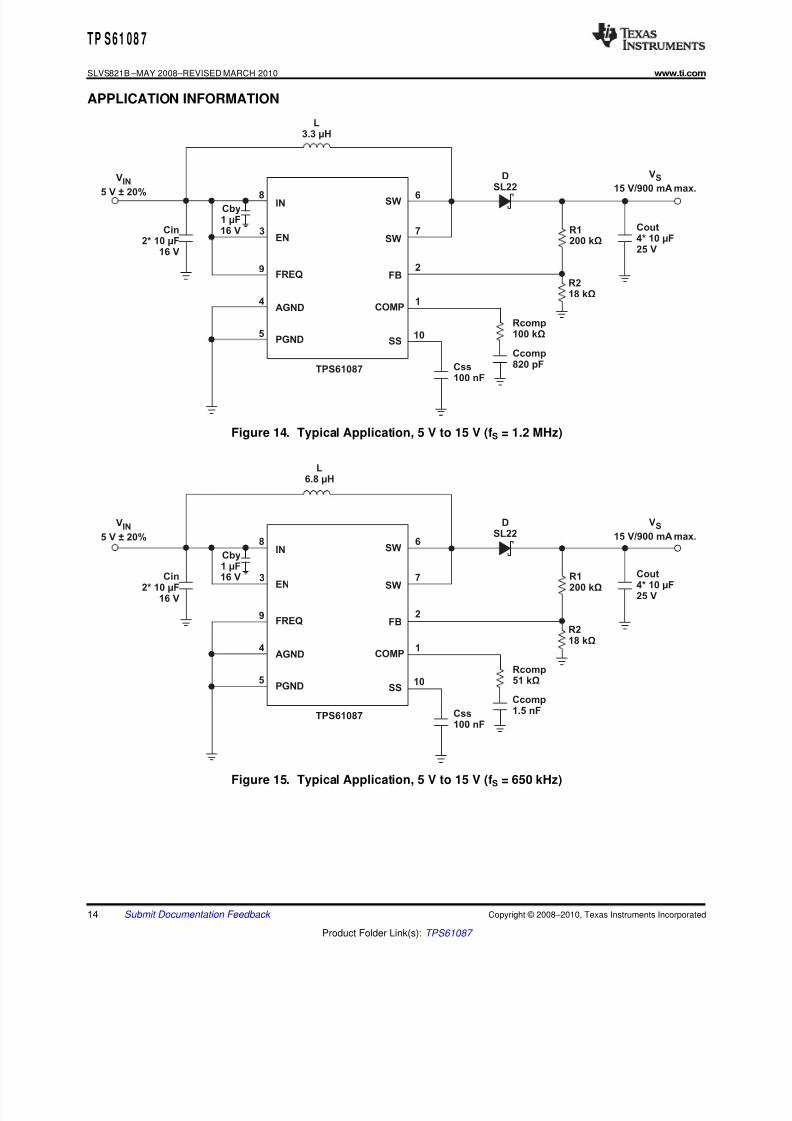
Figure 14. Typical Application, 5 V to 15 V (fS = 1.2 MHz)
Figure 15. Typical Application, 5 V to 15 V (fS = 650 kHz)
14 Submit Documentation Feedback Copyright © 2008–2010, Texas Instruments Incorporated
Product Folder Link(s): TPS61087
8/8/2019 Boost Convertor
http://slidepdf.com/reader/full/boost-convertor 15/28
IN
EN
SW
FBFREQ
AGND COMP
SS
14
68
3 7
2
5PGND
9
10
SW
Cby1µF16VCin
2*10µF16V
L3.3µH
DSL22
R218k
Cout4*10µF25V
Css100nF
TPS61087
V
3.3V±20%IN V
9V/950mA max.S
R1110k
Rcomp39k
Ccomp1.2nF
IN
EN
SW
FBFREQ
AGND COMP
SS
14
68
3 7
2
5PGND
9
10
SW
Cby1µF
16VCin2*10µF
16V
DSL22
R218k
Cout4*10µF25V
Css100nF
TPS61087
V
3.3V±20%IN
L6.8µH
V
9V/950mA max.S
R1110k
Rcomp18k
Ccomp2.7nF
TP S 61 08 7
www.ti.com SLVS821B –MAY 2008–REVISED MARCH 2010
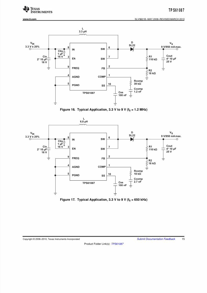
Figure 16. Typical Application, 3.3 V to 9 V (fS = 1.2 MHz)
Figure 17. Typical Application, 3.3 V to 9 V (fS = 650 kHz)
Copyright © 2008–2010, Texas Instruments Incorporated Submit Documentation Feedback 15
Product Folder Link(s): TPS61087

8/8/2019 Boost Convertor
http://slidepdf.com/reader/full/boost-convertor 16/28
V
5V±20%IN
IN
EN
SW
D
FBFREQ
AGND COMP
SL22
SS
14
68
3 7
2
5PGND
9
10
SW
TPS61087
Cin2*10µF/
16V
Cby1µF/16V
L6.8µH
Riso
10kW
BC857C
Ciso1µF/25V
Rcomp51k
Ccomp1.5nFCss
100nF
R1200k
R218k
Cout4*10µF/25V
V
15V/300mAS
Enable
IN
EN
SW
FBFREQ
AGND COMP
SS
14
68
3 7
2
5PGND
9
10
SW
Cby1µF16VCin
2*10µF
16V
DSL22
R1200k
R218k
Cout4*10µF
25V
Css100nF
TPS61087
V
5V±20%IN
L6.8µH
V
15V/900mA max.S
Rcomp51k
Ccomp1.5nF
Rlimit110
DzBZX84C18V
OvervoltageProtection
TP S 61 08 7
SLVS821B –MAY 2008–REVISED MARCH 2010 www.ti.com
Figure 18. Typical Application with External Load Disconnect Switch
Figure 19. Typical Application, 5 V to 15 V (fS = 1.2 MHz) with Overvoltage Protection
16 Submit Documentation Feedback Copyright © 2008–2010, Texas Instruments Incorporated
Product Folder Link(s): TPS61087

8/8/2019 Boost Convertor
http://slidepdf.com/reader/full/boost-convertor 17/28
C19470nF/50V
C18470nF/50V
T2BC850B
Vgh26.5V/20mA
IN
EN
SW
FB
Cout
FREQ
AGND COMP
4*10µF/
25V
SS
14
68
3 7
2
5PGND
9
10
SW
V
-7V/20mAGL
C201µF/35V
T1BC857B
R86.8k
D8BZX84C7V5
C14470nF/25V
-Vs
D4BAV99
C15470nF/50V
C16470nF/50V
C17470nF/50V
D3BAV99
D2BAV99
3·Vs
2·Vs
R1013k
D9BZX84C27V
L3.3µH
V
5V±20%IN
Cby1µF/16V
DSL22 V
15V/500mAS
R1200k
R218k
Rcomp100k
Ccomp820pF
Css100nF
Cin2*10µF/
16V
TPS61087
C131µF/35V
TP S 61 08 7
www.ti.com SLVS821B –MAY 2008–REVISED MARCH 2010
TFT LCD APPLICATION
Figure 20. Typical Application 5 V to 15 V (fS = 1.2 MHz) for TFT LCD with External Charge Pumps (VGH,VGL)
Copyright © 2008–2010, Texas Instruments Incorporated Submit Documentation Feedback 17
Product Folder Link(s): TPS61087
8/8/2019 Boost Convertor
http://slidepdf.com/reader/full/boost-convertor 18/28
IN
EN
SW
D
FBFREQ
AGND COMP
SL22
SS
14
68
3 7
2
5PGND
9
10
SW
TPS61087
V
5V±20%IN
Cin2*10µF/
16V
Cby1µF/16V
L6.8µH
Css100nF
Rcomp51k
Ccomp1.5nF
Rsense15
Cout4*10µF/25V
V
500mAS3S3P wLED
LWE67C
DzBZX84C18V
Rlimit110
optional
IN
EN
SW
D
FBFREQ
AGND COMP
SL22
SS
14
68
3 7
2
5PGND
9
10
SW
TPS61087
V
5V±20%IN
Cin2*10µF/
16V
Cby1µF/16V
L6.8µH
Css100nF
Rcomp51k
Ccomp1.5nF
Rsense15
Cout4*10µF/25V
V
500mAS3S3P wLED
LWE67C
DzBZX84C18V
Rlimit110
PWM100Hzto500Hz
optional
TP S 61 08 7
SLVS821B –MAY 2008–REVISED MARCH 2010 www.ti.com
WHITE LED APPLICATIONS
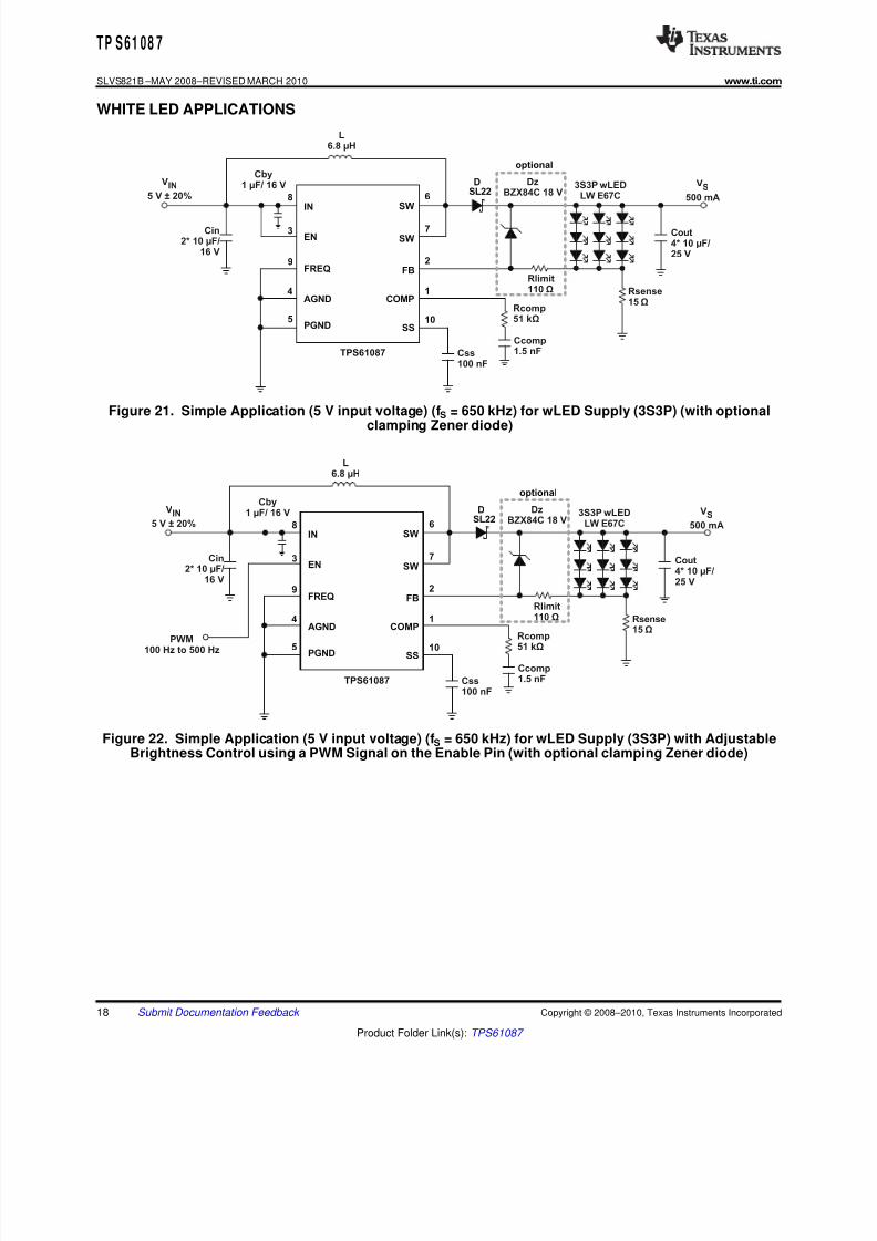
Figure 21. Simple Application (5 V input voltage) (fS = 650 kHz) for wLED Supply (3S3P) (with optionalclamping Zener diode)
Figure 22. Simple Application (5 V input voltage) (fS = 650 kHz) for wLED Supply (3S3P) with AdjustableBrightness Control using a PWM Signal on the Enable Pin (with optional clamping Zener diode)
18 Submit Documentation Feedback Copyright © 2008–2010, Texas Instruments Incorporated
Product Folder Link(s): TPS61087

8/8/2019 Boost Convertor
http://slidepdf.com/reader/full/boost-convertor 19/28
IN
EN
SW
D
FBFREQ
AGND COMP
SL22
SS
14
68
3 7
2
5PGND
9
10
SW
TPS61087
V
5V±20%IN
Cin2*10µF/
16V
Cby1µF/16V
L6.8µH
Css100nF
Rcomp51k
Ccomp1.5nF
Rsense15
Cout4*10µF/25V
V
500mAS3S3P wLED
LWE67C
DzBZX84C18V
RlimitR1
180k
AnalogBrightnessControl
PWMSignal
3.3V~wLEDoff 0V~l =30mA (eachstring)
Canbeusedswingingfrom0Vto3.3V
LED
R2127k
110
optional
TP S 61 08 7
www.ti.com SLVS821B –MAY 2008–REVISED MARCH 2010
Figure 23. Simple Application (5 V input voltage) (fS = 650 kHz) for wLED Supply (3S3P) with Adjustable
Brightness Control using an Analog Signal on the Feedback Pin (with optional clamping Zener diode)
Copyright © 2008–2010, Texas Instruments Incorporated Submit Documentation Feedback 19
Product Folder Link(s): TPS61087
8/8/2019 Boost Convertor
http://slidepdf.com/reader/full/boost-convertor 20/28
TP S 61 08 7
SLVS821B –MAY 2008–REVISED MARCH 2010 www.ti.com
REVISION HISTORY
Changes from Original (May 2008) to Revision A Page
• Added three paragraphs of text to the Detailed Description - following the Block Diagram ................................................. 8
Changes from Revision A (June 2008) to Revision B Page
• Added DSC device to top of front page ................................................................................................................................ 1
• Changed the Description to read From: The selectable frequency of 650 kHz and 1.2 MHz... To: The selectable
frequency of 650 kHz or 1.2 MHz ......................................................................................................................................... 1
• Added DSC package to ORDERING INFORMATION ......................................................................................................... 2
• Deleted Lead temperature from Absolute Maximum Ratings ............................................................................................... 2
• Changed Voltage on pin SW from 20 V to –0.3 to 20 V in Absolute Maximum Ratings ...................................................... 2
• Deleted RqJA from DISSIPATION RATINGS ......................................................................................................................... 2
• Changed fosc to fS in Electrical Characteristics Boost Converter Oscillator Frequency ............. .............. ............. .............. .. 3
• Changed FREQ = high to FREQ = VIN in Electrical Characteristics Boost Converter Oscillator Frequency ....................... 3
• Changed FREQ = low to FREQ = GND in Electrical Characteristics Boost Converter Oscillator Frequency ...................... 3• Added DSC package to PIN ASSIGNMENT ........................................................................................................................ 4
• Added Maximum load current vs. Input voltage graph ......................................................................................................... 4
• Added Maximum load current vs. Input voltage graph ......................................................................................................... 4
• Changed f to fS and Frequency to Oscillator Frequency in Figure 11 .................................................................................. 7
• Changed f to fS and Frequency to Oscillator Frequency in Figure 12 .................................................................................. 7
• Changed the text to the Detailed Description - reduced the numer of paragraphs from four to two. ................................... 8
• Changed the Design Procudures step 3 details - to make formulas easier to understand .................................................. 9
• Changed Inductor Selection text From: Typically, it is recommended that the inductor current ripple is below 20%
To: Typically, it is recommended that the inductor current ripple is below 35% ................................................................. 10
• Changed the format of Table 3 ........................................................................................................................................... 12
• Changed wording in Compensation description ................................................................................................................. 12• Added detailed information following Table 4 - to make formulas easier to understand .................................................... 12
• Changed wording in Thermal Shutdown section ................................................................................................................ 13
20 Submit Documentation Feedback Copyright © 2008–2010, Texas Instruments Incorporated
Product Folder Link(s): TPS61087
8/8/2019 Boost Convertor
http://slidepdf.com/reader/full/boost-convertor 21/28
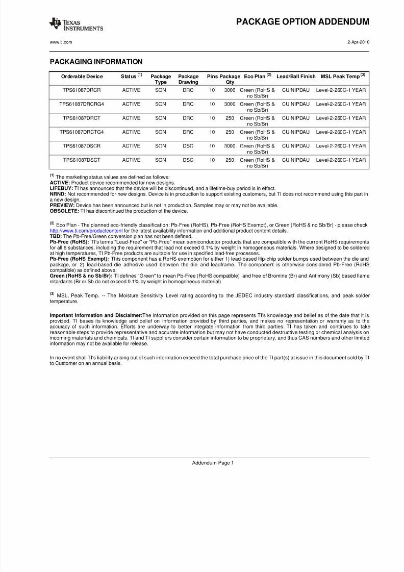
PACKAGING INFORMATION
Orderable Device Status (1) PackageType
PackageDrawing
Pins PackageQty
Eco Plan (2) Lead/Ball Finish MSL Peak Temp (3)
TPS61087DRCR ACTIVE SON DRC 10 3000 Green (RoHS &
no Sb/Br)
CU NIPDAU Level-2-260C-1 YEAR
TPS61087DRCRG4 ACTIVE SON DRC 10 3000 Green (RoHS &no Sb/Br)
CU NIPDAU Level-2-260C-1 YEAR
TPS61087DRCT ACTIVE SON DRC 10 250 Green (RoHS &no Sb/Br)
CU NIPDAU Level-2-260C-1 YEAR
TPS61087DRCTG4 ACTIVE SON DRC 10 250 Green (RoHS &no Sb/Br)
CU NIPDAU Level-2-260C-1 YEAR
TPS61087DSCR ACTIVE SON DSC 10 3000 Green (RoHS &no Sb/Br)
CU NIPDAU Level-2-260C-1 YEAR
TPS61087DSCT ACTIVE SON DSC 10 250 Green (RoHS &no Sb/Br)
CU NIPDAU Level-2-260C-1 YEAR
(1)The marketing status values are defined as follows:
ACTIVE: Product device recommended for new designs.LIFEBUY: TI has announced that the device will be discontinued, and a lifetime-buy period is in effect.NRND: Not recommended for new designs. Device is in production to support existing customers, but TI does not recommend using this part ina new design.PREVIEW: Device has been announced but is not in production. Samples may or may not be available.OBSOLETE: TI has discontinued the production of the device.
(2) Eco Plan - The planned eco-friendly classification: Pb-Free (RoHS), Pb-Free (RoHS Exempt), or Green (RoHS & no Sb/Br) - please checkhttp://www.ti.com/productcontent for the latest availability information and additional product content details.TBD: The Pb-Free/Green conversion plan has not been defined.Pb-Free (RoHS): TI's terms "Lead-Free" or "Pb-Free" mean semiconductor products that are compatible with the current RoHS requirementsfor all 6 substances, including the requirement that lead not exceed 0.1% by weight in homogeneous materials. Where designed to be solderedat high temperatures, TI Pb-Free products are suitable for use in specified lead-free processes.Pb-Free (RoHS Exempt): This component has a RoHS exemption for either 1) lead-based flip-chip solder bumps used between the die andpackage, or 2) lead-based die adhesive used between the die and leadframe. The component is otherwise considered Pb-Free (RoHScompatible) as defined above.Green (RoHS & no Sb/Br): TI defines "Green" to mean Pb-Free (RoHS compatible), and free of Bromine (Br) and Antimony (Sb) based flameretardants (Br or Sb do not exceed 0.1% by weight in homogeneous material)
(3) MSL, Peak Temp. -- The Moisture Sensitivity Level rating according to the JEDEC industry standard classifications, and peak soldertemperature.
Important Information and Disclaimer:The information provided on this page represents TI's knowledge and belief as of the date that it isprovided. TI bases its knowledge and belief on information provided by third parties, and makes no representation or warranty as to theaccuracy of such information. Efforts are underway to better integrate information from third parties. TI has taken and continues to takereasonable steps to provide representative and accurate information but may not have conducted destructive testing or chemical analysis onincoming materials and chemicals. TI and TI suppliers consider certain information to be proprietary, and thus CAS numbers and other limitedinformation may not be available for release.
In no event shall TI's liability arising out of such information exceed the total purchase price of the TI part(s) at issue in this document sold by TIto Customer on an annual basis.
PACKAGE OPTION ADDENDUM
www.ti.com 2-Apr-2010
Addendum-Page 1
8/8/2019 Boost Convertor
http://slidepdf.com/reader/full/boost-convertor 22/28
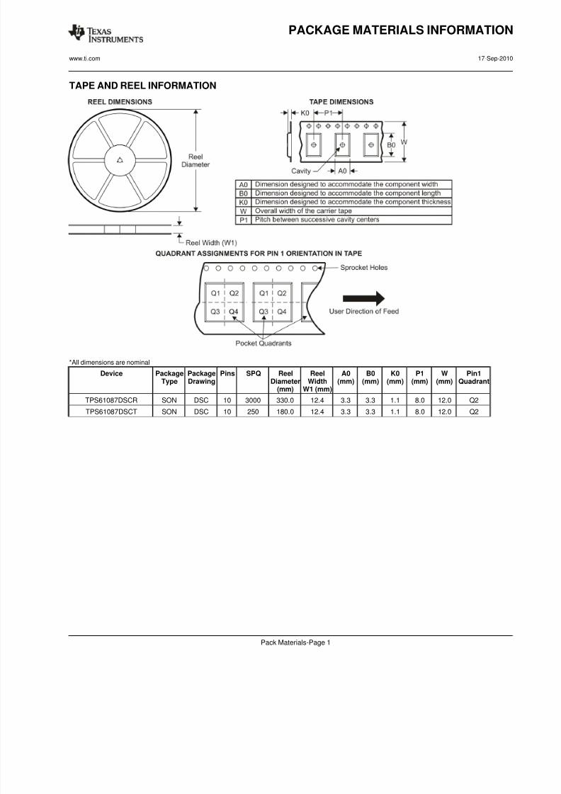
TAPE AND REEL INFORMATION
*All dimensions are nominal
Device PackageType
PackageDrawing
Pins SPQ ReelDiameter
(mm)
ReelWidth
W1 (mm)
A0(mm)
B0(mm)
K0(mm)
P1(mm)
W(mm)
Pin1Quadrant
TPS61087DSCR SON DSC 10 3000 330.0 12.4 3.3 3.3 1.1 8.0 12.0 Q2
TPS61087DSCT SON DSC 10 250 180.0 12.4 3.3 3.3 1.1 8.0 12.0 Q2
PACKAGE MATERIALS INFORMATION
www.ti.com 17-Sep-2010
Pack Materials-Page 1
8/8/2019 Boost Convertor
http://slidepdf.com/reader/full/boost-convertor 23/28
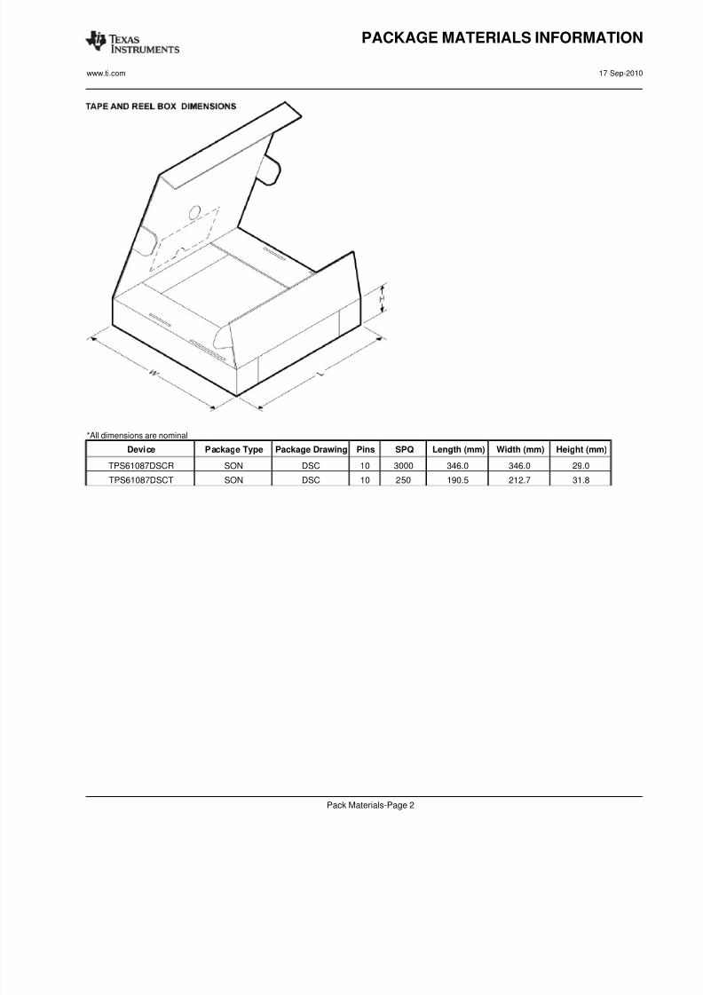
*All dimensions are nominal
Device Package Type Package Drawing Pins SPQ Length (mm) Width (mm) Height (mm)
TPS61087DSCR SON DSC 10 3000 346.0 346.0 29.0
TPS61087DSCT SON DSC 10 250 190.5 212.7 31.8
PACKAGE MATERIALS INFORMATION
www.ti.com 17-Sep-2010
Pack Materials-Page 2
8/8/2019 Boost Convertor
http://slidepdf.com/reader/full/boost-convertor 24/28

8/8/2019 Boost Convertor
http://slidepdf.com/reader/full/boost-convertor 25/28
8/8/2019 Boost Convertor
http://slidepdf.com/reader/full/boost-convertor 26/28
8/8/2019 Boost Convertor
http://slidepdf.com/reader/full/boost-convertor 27/28
8/8/2019 Boost Convertor
http://slidepdf.com/reader/full/boost-convertor 28/28
IMPORTANT NOTICE
Texas Instruments Incorporated and its subsidiaries (TI) reserve the right to make corrections, modifications, enhancements, improvements,and other changes to its products and services at any time and to discontinue any product or service without notice. Customers shouldobtain the latest relevant information before placing orders and should verify that such information is current and complete. All products aresold subject to TI’s terms and conditions of sale supplied at the time of order acknowledgment.
TI warrants performance of its hardware products to the specifications applicable at the time of sale in accordance with TI’s standardwarranty. Testing and other quality control techniques are used to the extent TI deems necessary to support this warranty. Except where
mandated by government requirements, testing of all parameters of each product is not necessarily performed.
TI assumes no liability for applications assistance or customer product design. Customers are responsible for their products andapplications using TI components. To minimize the risks associated with customer products and applications, customers should provideadequate design and operating safeguards.
TI does not warrant or represent that any license, either express or implied, is granted under any TI patent right, copyright, mask work right,or other TI intellectual property right relating to any combination, machine, or process in which TI products or services are used. Informationpublished by TI regarding third-party products or services does not constitute a license from TI to use such products or services or awarranty or endorsement thereof. Use of such information may require a license from a third party under the patents or other intellectualproperty of the third party, or a license from TI under the patents or other intellectual property of TI.
Reproduction of TI information in TI data books or data sheets is permissible only if reproduction is without alteration and is accompaniedby all associated warranties, conditions, limitations, and notices. Reproduction of this information with alteration is an unfair and deceptivebusiness practice. TI is not responsible or liable for such altered documentation. Information of third parties may be subject to additionalrestrictions.
Resale of TI products or services with statements different from or beyond the parameters stated by TI for that product or service voids allexpress and any implied warranties for the associated TI product or service and is an unfair and deceptive business practice. TI is not
responsible or liable for any such statements.
TI products are not authorized for use in safety-critical applications (such as life support) where a failure of the TI product would reasonablybe expected to cause severe personal injury or death, unless officers of the parties have executed an agreement specifically governingsuch use. Buyers represent that they have all necessary expertise in the safety and regulatory ramifications of their applications, andacknowledge and agree that they are solely responsible for all legal, regulatory and safety-related requirements concerning their productsand any use of TI products in such safety-critical applications, notwithstanding any applications-related information or support that may beprovided by TI. Further, Buyers must fully indemnify TI and its representatives against any damages arising out of the use of TI products insuch safety-critical applications.
TI products are neither designed nor intended for use in military/aerospace applications or environments unless the TI products arespecifically designated by TI as military-grade or "enhanced plastic." Only products designated by TI as military-grade meet militaryspecifications. Buyers acknowledge and agree that any such use of TI products which TI has not designated as military-grade is solely atthe Buyer's risk, and that they are solely responsible for compliance with all legal and regulatory requirements in connection with such use.
TI products are neither designed nor intended for use in automotive applications or environments unless the specific TI products aredesignated by TI as compliant with ISO/TS 16949 requirements. Buyers acknowledge and agree that, if they use any non-designatedproducts in automotive applications, TI will not be responsible for any failure to meet such requirements.
Following are URLs where you can obtain information on other Texas Instruments products and application solutions:
Products Applications
Amplifiers amplifier.ti.com Audio www.ti.com/audio
Data Converters dataconverter.ti.com Automotive www.ti.com/automotive
DLP® Products www.dlp.com Communications and www.ti.com/communicationsTelecom
DSP dsp.ti.com Computers and www.ti.com/computersPeripherals
Clocks and Timers www.ti.com/clocks Consumer Electronics www.ti.com/consumer-apps
Interface interface.ti.com Energy www.ti.com/energy
Logic logic.ti.com Industrial www.ti.com/industrial
Power Mgmt power.ti.com Medical www.ti.com/medical
Microcontrollers microcontroller.ti.com Security www.ti.com/security
RFID www.ti-rfid.com Space, Avionics & www.ti.com/space-avionics-defenseDefense
RF/IF and ZigBee® Solutions www.ti.com/lprf Video and Imaging www.ti.com/video
Wireless www.ti.com/wireless-apps
Mailing Address: Texas Instruments, Post Office Box 655303, Dallas, Texas 75265Copyright © 2010, Texas Instruments Incorporated