Embed Size (px)
Citation preview
ACCESS IC LAB
Graduate Institute of Electronics Engineering, NTU
CH16 Sequential Circuit DesignCH16 Sequential Circuit Design
Lecturer:吳安宇 教授
Date:2007/1/5Ver 1.1

Graduate Institute of Electronics Engineering, NTU
pp. 2台灣大學 吳安宇 教授
OutlineOutline
16.1 Summary of Design Procedure forSequential Circuits
16.2 Design Example-Code Converter
16.3 Design of Iterative CircuitsDesign of a Comparator
16.4 Design of Sequential Circuits UsingROMs and PLAs

Graduate Institute of Electronics Engineering, NTU
pp. 3台灣大學 吳安宇 教授
Design ExampleDesign Example--Code ConverterCode Converter
Adds 3 to BCD code (0~9)Serial I/O with the LSB first
x0 x1 x2 x3
z0 z1 z2 z3
Reset to initial state after receiving four inputs
Code
Converterx3x2x1x0 z3z2z1z0
t3 t2 t1 t0 t3 t2 t1 t0
X = (x3x2x1x0), Z = (z3z2z1z0)
BCD code Excess-3 code
(1010 ~ 1111) x x x x
Graduate Institute of Electronics Engineering, NTU
pp. 4台灣大學 吳安宇 教授
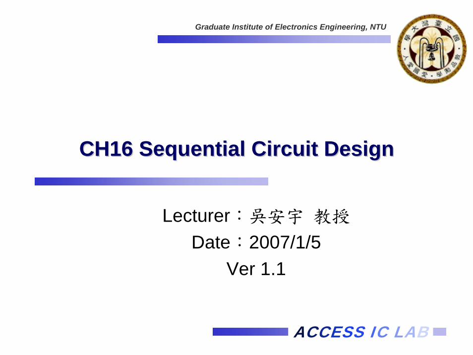
Design ExampleDesign Example--Code ConverterCode ConverterState Table for Code Converter
State Graph for Code Converterstep1
Step2: Reduce the table using row matchingWatch the effects of “X”!!

Graduate Institute of Electronics Engineering, NTU
pp. 5台灣大學 吳安宇 教授
Serial Code ConverterSerial Code ConverterReduced State Table for Code Converter
GFGFE
LKJILKJIH
PNPNM
, eliminate
, , , eliminate
, eliminate
⇒≡≡
⇒≡≡≡≡
⇒≡≡
step2
After elimination, the state table reduces to 7 rows.
Graduate Institute of Electronics Engineering, NTU
pp. 6台灣大學 吳安宇 教授
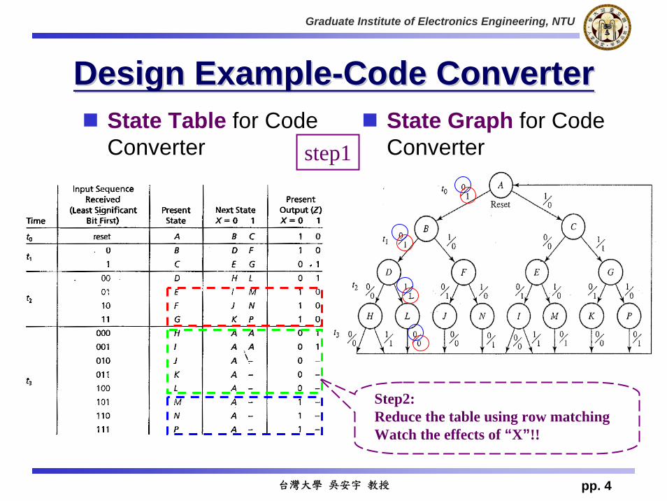
Serial Code ConverterSerial Code ConverterImplementation:Assignment Map and Transition Table for Flip-Flops
7 states 3 flip-flops are requiredstep3~4
(A better way can be examined!)
--
Z=f (Q1,Q2,Q3,X)
0
1236754
XQ1Q2Q3

Graduate Institute of Electronics Engineering, NTU
pp. 7台灣大學 吳安宇 教授
Construct Truth TableConstruct Truth Table
Graduate Institute of Electronics Engineering, NTU
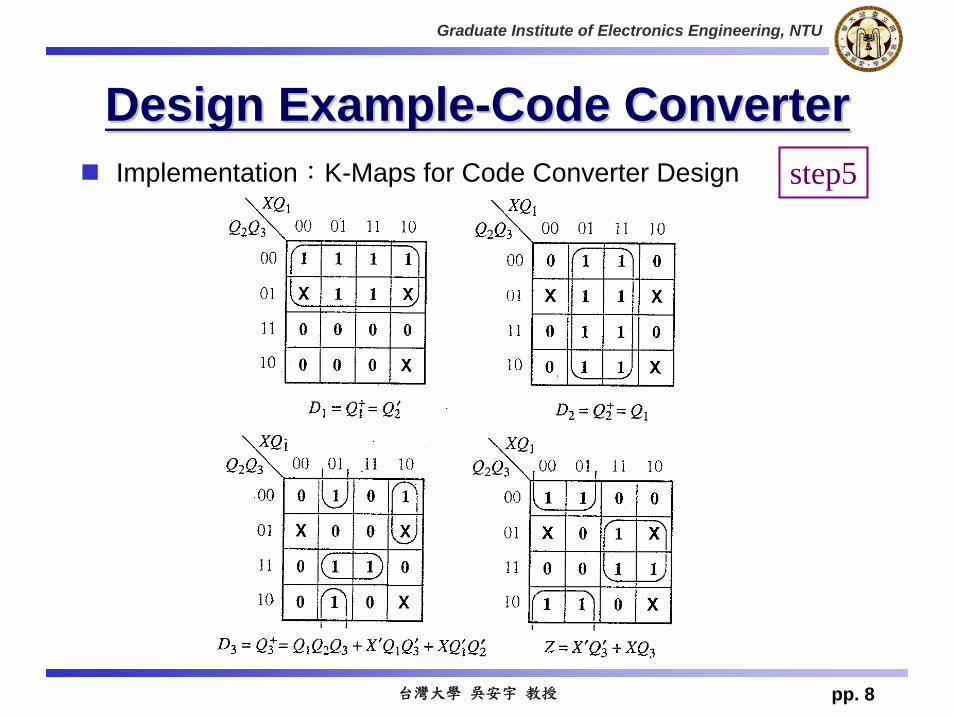
pp. 8台灣大學 吳安宇 教授
Design ExampleDesign Example--Code ConverterCode ConverterImplementation:K-Maps for Code Converter Design step5

Graduate Institute of Electronics Engineering, NTU
pp. 9台灣大學 吳安宇 教授
Design Example Design Example -- Code ConverterCode Converter
Implementation:Code Converter Circuit step6
Output function
StatesCombinational Circuits
Graduate Institute of Electronics Engineering, NTU
pp. 10台灣大學 吳安宇 教授
OutlineOutline
16.1 Summary of Design Procedure forSequential Circuits
16.2 Design Example-Code Converter16.3 Design of Iterative Circuits
Design of a Comparator16.4 Design of Sequential Circuits Using
ROMs and PLAs

Graduate Institute of Electronics Engineering, NTU
pp. 11台灣大學 吳安宇 教授
Design of Iterative CircuitsDesign of Iterative CircuitsUnilateral Iterative Circuit
Regular structure:Parallel-input, parallel-output
Xi:input , Zi:outputai+1 ai (state)
Unilateral Iterative Circuit is very similar tothe design of a sequential circuit

Graduate Institute of Electronics Engineering, NTU
pp. 12台灣大學 吳安宇 教授
Design of a Design of a SequentialSequential ComparatorComparatorForm of Iterative Circuit for Comparing Binary Numbers
X = { x1x2.....xn } Y = { y1y2.....yn } x1,y1:MSB (most significant bit)
time t1 t2 tn
Graduate Institute of Electronics Engineering, NTU
pp. 13台灣大學 吳安宇 教授
Design of a Sequential ComparatorDesign of a Sequential Comparator
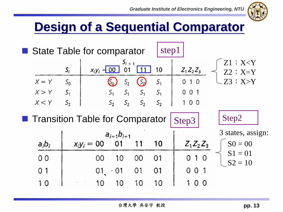
State Table for comparator
Transition Table for Comparator
step1Z1:X<YZ2:X=YZ3:X>Y
3 states, assign:S0 = 00S1 = 01S2 = 10
Step2Step3
Graduate Institute of Electronics Engineering, NTU
pp. 14台灣大學 吳安宇 教授
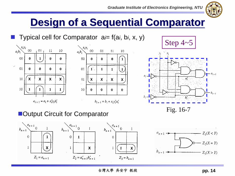
Design of a Sequential ComparatorDesign of a Sequential ComparatorTypical cell for Comparator ai= f(ai, bi, x, y)
Step 4~5
Output Circuit for ComparatorFig. 16-7

Graduate Institute of Electronics Engineering, NTU
pp. 15台灣大學 吳安宇 教授
Complete Iterative Comparator CircuitComplete Iterative Comparator CircuitX = { x1x2.....xn } Y = { y1y2.....yn }
time t1 t2 tn
x1,y1:MSB (most significant bit)xn,yn:LSB (least significant bit)

Graduate Institute of Electronics Engineering, NTU
pp. 16台灣大學 吳安宇 教授
OutlineOutline
16.1 Summary of Design Procedure forSequential Circuits
16.2 Design Example-Code Converter16.3 Design of Iterative Circuits
Design of a Comparator16.4 Design of Sequential Circuits Using
ROMs and PLAs

Graduate Institute of Electronics Engineering, NTU
pp. 17台灣大學 吳安宇 教授
Design of Sequential Circuits Using Design of Sequential Circuits Using ROMs and ROMs and PLAsPLAs
Realize Code Converter using a ROM and D filp-flops

Graduate Institute of Electronics Engineering, NTU
pp. 18台灣大學 吳安宇 教授
Design of Sequential Circuits Using Design of Sequential Circuits Using ROMs and ROMs and PLAsPLAs
ROM contents
Input
Address
ROM
a3
a2
a1
a0
Z D1 D2 D3

Graduate Institute of Electronics Engineering, NTU
pp. 19台灣大學 吳安宇 教授
Design of Sequential Circuits Using Design of Sequential Circuits Using ROMs and ROMs and PLAsPLAs (using D flip(using D flip--flops)flops)

Graduate Institute of Electronics Engineering, NTU
pp. 20台灣大學 吳安宇 教授
Design of Code Converter Using Design of Code Converter Using PLAsPLAs
Graduate Institute of Electronics Engineering, NTU
pp. 21台灣大學 吳安宇 教授
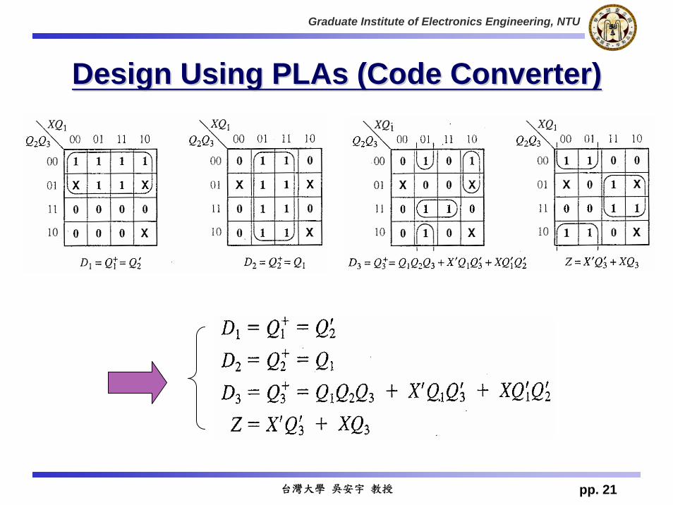
Design Using Design Using PLAsPLAs (Code Converter)(Code Converter)
Graduate Institute of Electronics Engineering, NTU
pp. 22台灣大學 吳安宇 教授
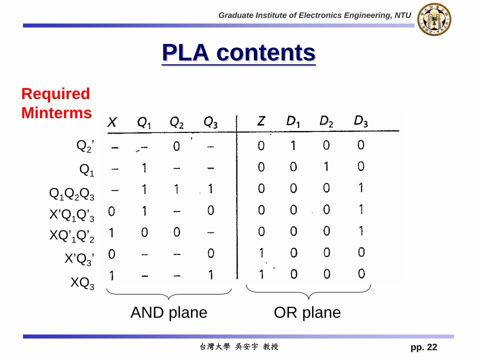
Q2’
Q1
Q1Q2Q3
X’Q1Q’3XQ’1Q’2
X’Q3’
XQ3
AND plane OR plane
PLA contentsPLA contentsRequiredMinterms
Graduate Institute of Electronics Engineering, NTU
pp. 23台灣大學 吳安宇 教授
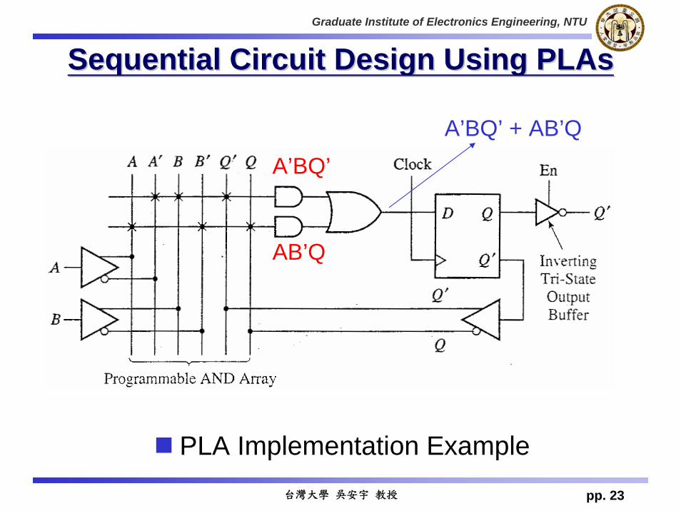
Sequential Circuit Design Using Sequential Circuit Design Using PLAsPLAs
PLA Implementation Example
A’BQ’
AB’Q
A’BQ’ + AB’Q

Graduate Institute of Electronics Engineering, NTU
pp. 24台灣大學 吳安宇 教授
Sec. 16.1: Design Procedure for Sec. 16.1: Design Procedure for Sequential CircuitsSequential Circuits
1. Given the problem statement, determine the relationship between input and output Derive a state table (graph).
2. Reduce the table to a minimum number of states.
3. Assign a unique combination of flip-flop states to correspond to each state in the reduced table.
4. Form the transition table.
5. Plot next-state maps and input maps for each flip-flop. Derive the flip-flop input equations. Derive the output equations.
6. Realize the flip-flop input equations and the output equations.
7. Check your design by signal tracing, computer simulation, or laboratory testing.