Embed Size (px)
DESCRIPTION
Chapter 3 and 4 TEM Crystallography and Diffraction
Citation preview
7/18/2019 Chapter 3 and 4 TEM Crystallography and Diffraction
http://slidepdf.com/reader/full/chapter-3-and-4-tem-crystallography-and-diffraction 1/29
Duncan Alexander : TEM Crystallography and Diffraction CIME, EPFL
TEM Crystallographyand Diffraction
1
Duncan Alexander EPFL-CIME
Duncan Alexander : TEM Crystallography and Diffraction CIME, EPFL
Contents
• Introduction to electron diffraction
• Basic crystallography and symmetry
•Electron diffraction theory
• Scattering from slits
• Bragg law
• Reciprocal lattice and Ewald sphere
• Relrods and diffraction spot intensity
•Elastic scattering theory
2
7/18/2019 Chapter 3 and 4 TEM Crystallography and Diffraction
http://slidepdf.com/reader/full/chapter-3-and-4-tem-crystallography-and-diffraction 2/29
Duncan Alexander : TEM Crystallography and Diffraction CIME, EPFL
Introduction toelectron diffraction
3
Duncan Alexander : TEM Crystallography and Diffraction CIME, EPFL
Diffraction: constructive and destructive interference of waves
! electrons interact very strongly with matter => strong diffraction intensity(can take patterns in seconds, unlike X-ray diffraction)
" diffraction from only selected set of planes in one pattern - e.g. only 2D information
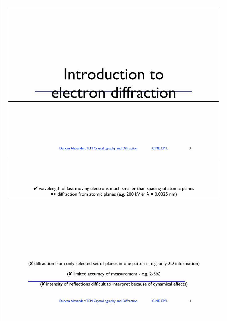
! wavelength of fast moving electrons much smaller than spacing of atomic planes=> diffraction from atomic planes (e.g. 200 kV e-, " = 0.0025 nm)
! spatially-localized information (! 200 nm for selected-area diffraction; 2 nm possible with convergent-beam electron diffraction)
! orientation information
! close relationship to diffraction contrast in imaging
! immediate in the TEM!
" limited accuracy of measurement - e.g. 2-3%
" intensity of reflections difficult to interpret because of dynamical effects
Why use electron diffraction?
4
(" diffraction from only selected set of planes in one pattern - e.g. only 2D information)
(" limited accuracy of measurement - e.g. 2-3%)
(" intensity of reflections difficult to interpret because of dynamical effects)
7/18/2019 Chapter 3 and 4 TEM Crystallography and Diffraction
http://slidepdf.com/reader/full/chapter-3-and-4-tem-crystallography-and-diffraction 3/29
Duncan Alexander : TEM Crystallography and Diffraction CIME, EPFL
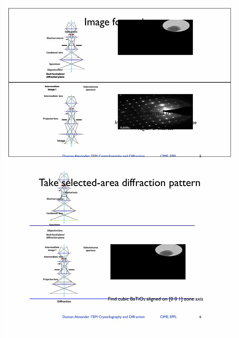
Insert selected area aperture to chooseregion of interest
Optical axis
Electron source
Condenser lens
Specimen
Objective lens
Back focal plane/
diff raction plane
Intermediate lens
Projector lens
Image
Intermediate
image 1
Optical axis
Electron source
Condenser lens
Specimen
Objective lens
Back focal plane/
diff raction plane
Intermediate lens
Projector lens
Image
Intermediate
image 1Selected area
aperture
BaTiO3 nanocrystals (Psaltis lab)
Image formation
5
Duncan Alexander : TEM Crystallography and Diffraction CIME, EPFL
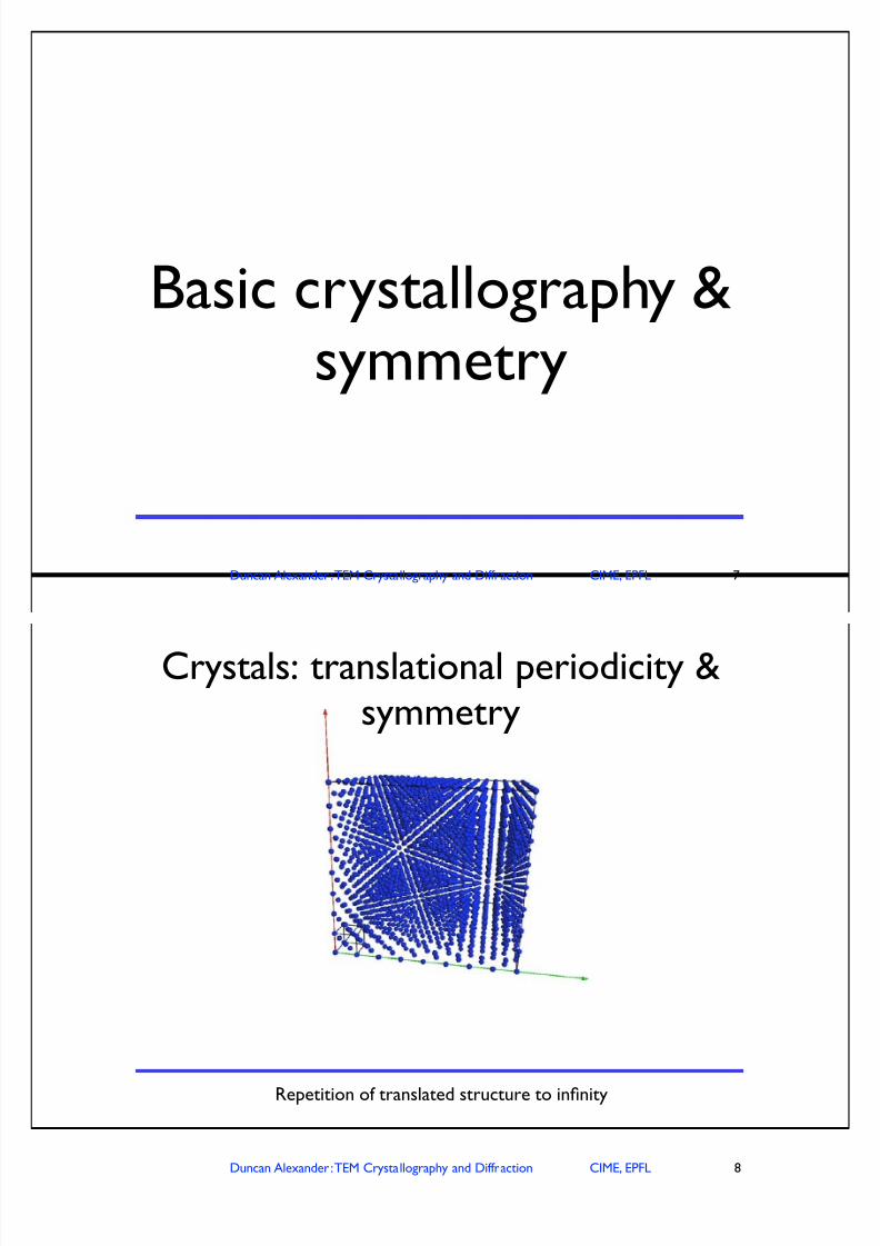
Press “D” for diffraction on microscope console -alter strength of intermediate lens and focus
diffraction pattern on to screen
Optical axis
Electron source
Condenser lens
Specimen
Objective lens
Back focal plane/
diff raction plane
Intermediate lens
Projector lens
Image
Intermediate
image 1Selected area
aperture
Optical axis
Electron source
Condenser lens
Specimen
Objective lens
Back focal plane/
diff raction plane
Intermediate lens
Projector lens
Diff raction
Intermediate
image 1Selected area
aperture
Find cubic BaTiO3 aligned on [0 0 1] zone axis
Take selected-area diffraction pattern
6
7/18/2019 Chapter 3 and 4 TEM Crystallography and Diffraction
http://slidepdf.com/reader/full/chapter-3-and-4-tem-crystallography-and-diffraction 4/29
Duncan Alexander : TEM Crystallography and Diffraction CIME, EPFL
Basic crystallography &symmetry
7
Duncan Alexander : TEM Crystallography and Diffraction CIME, EPFL
Repetition of translated structure to infinity
Crystals: translational periodicity &symmetry
8
7/18/2019 Chapter 3 and 4 TEM Crystallography and Diffraction
http://slidepdf.com/reader/full/chapter-3-and-4-tem-crystallography-and-diffraction 5/29
Duncan Alexander : TEM Crystallography and Diffraction CIME, EPFL
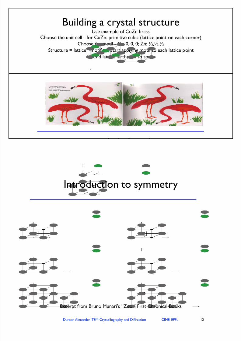
Unit cell is the smallest repeating unit of the crystal lattice Has a lattice point on each corner (and perhaps more elsewhere)
Defined by lattice parameters a, b, c along axes x , y , zand angles between crystallographic axes:# = b^c ;$ = a^c ; % = a^b
Crystallography: the unit cell
9
Duncan Alexander : TEM Crystallography and Diffraction CIME, EPFL
Use example of CuZn brassChoose the unit cell - for CuZn: primitive cubic (lattice point on each corner)
x
y
z
Choose the motif - Cu: 0, 0, 0; Zn: ",","
x
y
z
Motif:Cu
Zn
x
y
z
Structure = lattice +motif => Start applying motif to each lattice point
x
y
z
Motif:Cu
Zn
x
y
z
x
y
z
Motif:Cu
Zn
x
y
z
Building a crystal structure
10
7/18/2019 Chapter 3 and 4 TEM Crystallography and Diffraction
http://slidepdf.com/reader/full/chapter-3-and-4-tem-crystallography-and-diffraction 6/29
Duncan Alexander : TEM Crystallography and Diffraction CIME, EPFL
x
y
z
Motif:
Cu
Zn
x
y
z
Use example of CuZn brassChoose the unit cell - for CuZn: primitive cubic (lattice point on each corner)
Choose the motif - Cu: 0, 0, 0; Zn: ",","
Structure = lattice +motif => Start applying motif to each lattice point
Extend lattice further in to space
x
y
z
Cu
Zn
x
y
z
Cu
Zn
x
y
z
Cu
Zn
y
x
y
zCu
Zn
y
y
x
y
zCu
Zn
y
y
y
x
y
zCu
Zn
y
y
y
y
Building a crystal structure
11
Duncan Alexander : TEM Crystallography and Diffraction CIME, EPFL
Introduction to symmetry
12
Flamingos
know
they
are beautiful
and strange,
and play
at symmetry.
\,t
4r
l
T
al
\/ \
/\
/
\ / I V
\ 1
\ X Y \ \
q
l
\
Excerpt from Bruno Munari’s “Zoo”, First Chronical Books
7/18/2019 Chapter 3 and 4 TEM Crystallography and Diffraction
http://slidepdf.com/reader/full/chapter-3-and-4-tem-crystallography-and-diffraction 7/29
Duncan Alexander : TEM Crystallography and Diffraction CIME, EPFL
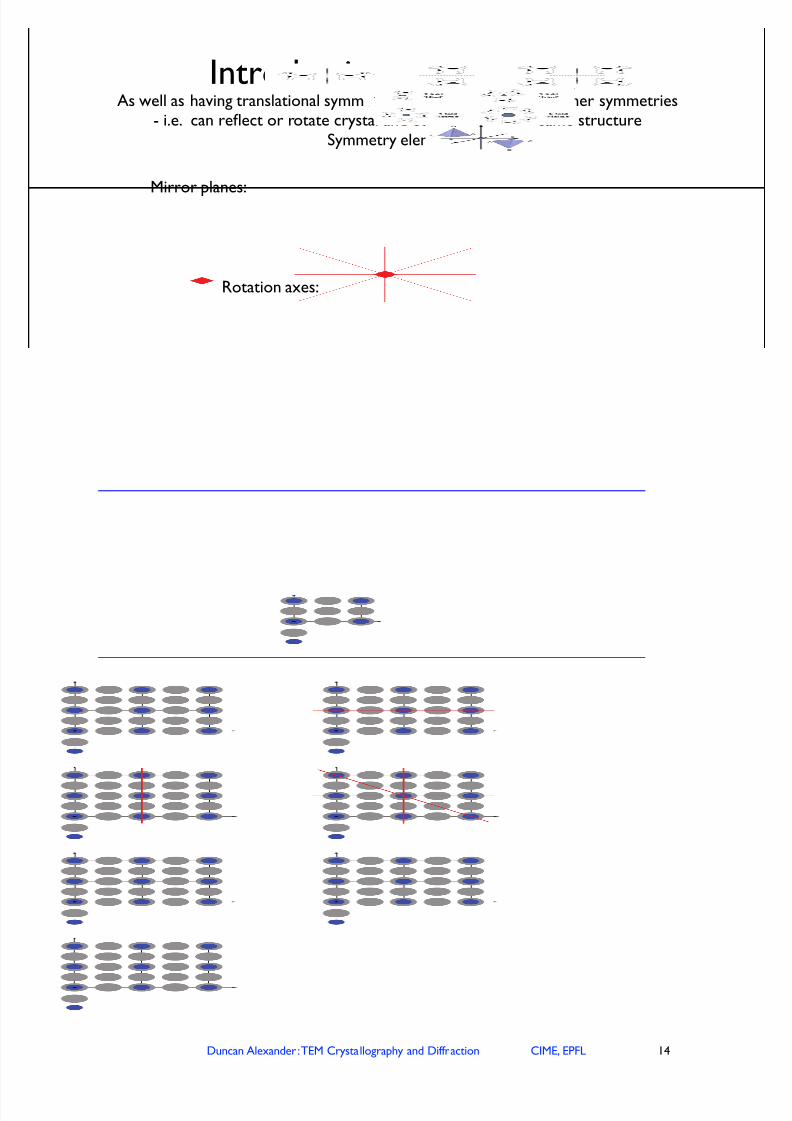
As well as having translational symmetry, nearly all crystals obey other symmetries- i.e. can reflect or rotate crystal and obtain exactly the same structure
Symmetry elements:
Mirror planes:
Rotation axes:
Inversion axes: combination of rotation axis with centre of symmetry
Centre of symmetry or inversion centre:
Introduction to symmetry
13
Duncan Alexander : TEM Crystallography and Diffraction CIME, EPFL
Example - Tetragonal lattice:a = b & c ;# = $ = % = 90°
Anatase TiO2 (body-centred lattice) view down [0 0 1] ( z-axis):
x
y
z
O
Ti
x
y
z
O
Ti
Identify mirror planes
x
y
z
O
Ti
x
y
z
O
Ti
x
y
z
O
Ti
x
y
z
O
Ti
x
y
z
O
Ti
x
y
z
O
Ti
Tetrad:
4-fold rotation
axis
Mirror plane
Identify rotation axis: 4-fold = defining symmetry of tetragonal lattice!
Introduction to symmetry
14
7/18/2019 Chapter 3 and 4 TEM Crystallography and Diffraction
http://slidepdf.com/reader/full/chapter-3-and-4-tem-crystallography-and-diffraction 8/29
Duncan Alexander : TEM Crystallography and Diffraction CIME, EPFL
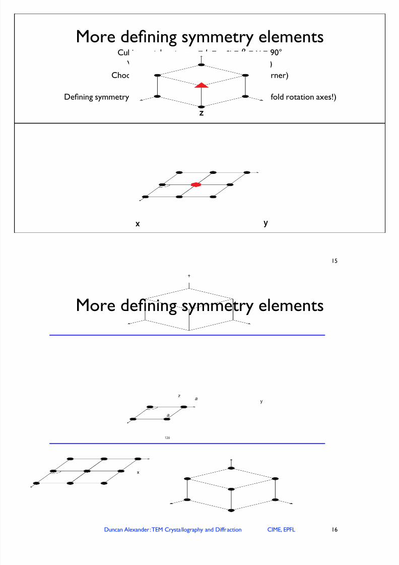
Cubic crystal system: a = b = c ;# = $ = % = 90°
View down body diagonal (i.e. [1 1 1] axis)
Choose Primitive cell (lattice point on each corner)
Identify rotation axis: 3-fold (triad)
Defining symmetry of cube: four 3-fold rotation axes (not 4-fold rotation axes!)
x y
z
x y
z
x y
z
More defining symmetry elements
15
Duncan Alexander : TEM Crystallography and Diffraction CIME, EPFL
Hexagonal crystal system: a = b & c ;# = $ = 90°, % = 120°
Primitive cell, lattice points on each corner; view down z-axis - i.e.[1 0 0]
x
y
z
120
a
a
Draw 2 x 2 unit cells
Identify rotation axis: 6-fold (hexad) - defining symmetry of hexagonal lattice
x
yz
120
a
a
x
yz
120
a
a
More defining symmetry elements
16
7/18/2019 Chapter 3 and 4 TEM Crystallography and Diffraction
http://slidepdf.com/reader/full/chapter-3-and-4-tem-crystallography-and-diffraction 9/29
Duncan Alexander : TEM Crystallography and Diffraction CIME, EPFL
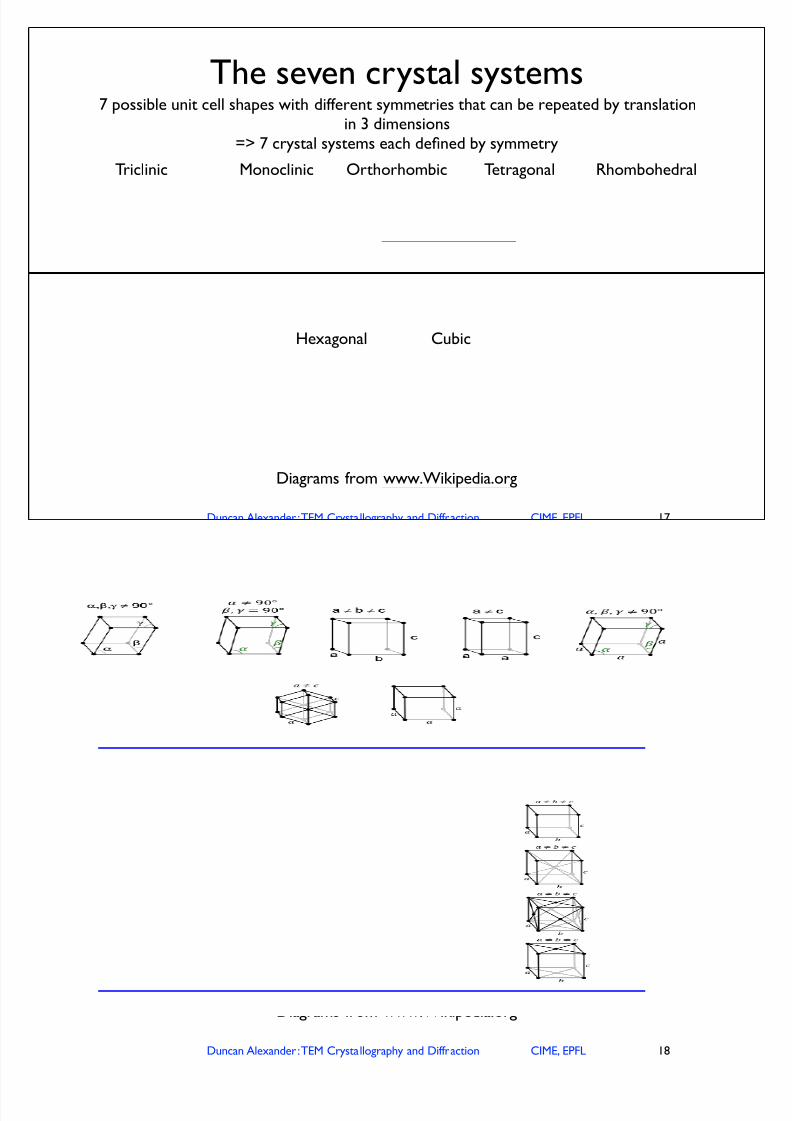
7 possible unit cell shapes with different symmetries that can be repeated by translationin 3 dimensions
=> 7 crystal systems each defined by symmetry
Triclinic Monoclinic Orthorhombic Tetragonal Rhombohedral
Hexagonal Cubic
Diagrams from www.Wikipedia.org
The seven crystal systems
17
Duncan Alexander : TEM Crystallography and Diffraction CIME, EPFL
P: Primitive - lattice points on cell corners
I: Body-centred - additional lattice point at cell centre
F: Face-centred - one additional lattice point at centreof each face
A/B/C: Centred on a single face - one additional lattice
point centred on A, B or C face
Diagrams from www.Wikipedia.org
Four possible lattice centerings
18
7/18/2019 Chapter 3 and 4 TEM Crystallography and Diffraction
http://slidepdf.com/reader/full/chapter-3-and-4-tem-crystallography-and-diffraction 10/29
Duncan Alexander : TEM Crystallography and Diffraction CIME, EPFL
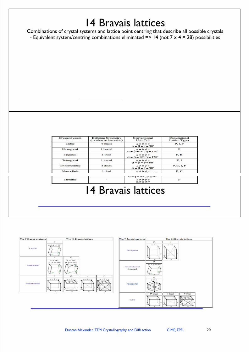
Combinations of crystal systems and lattice point centring that describe all possible crystals - Equivalent system/centring combinations eliminated => 14 (not 7 x 4 = 28) possibilities
Diagrams from www.Wikipedia.org
14 Bravais lattices
19
Duncan Alexander : TEM Crystallography and Diffraction CIME, EPFL
14 Bravais lattices
20
7/18/2019 Chapter 3 and 4 TEM Crystallography and Diffraction
http://slidepdf.com/reader/full/chapter-3-and-4-tem-crystallography-and-diffraction 11/29
Duncan Alexander : TEM Crystallography and Diffraction CIME, EPFL
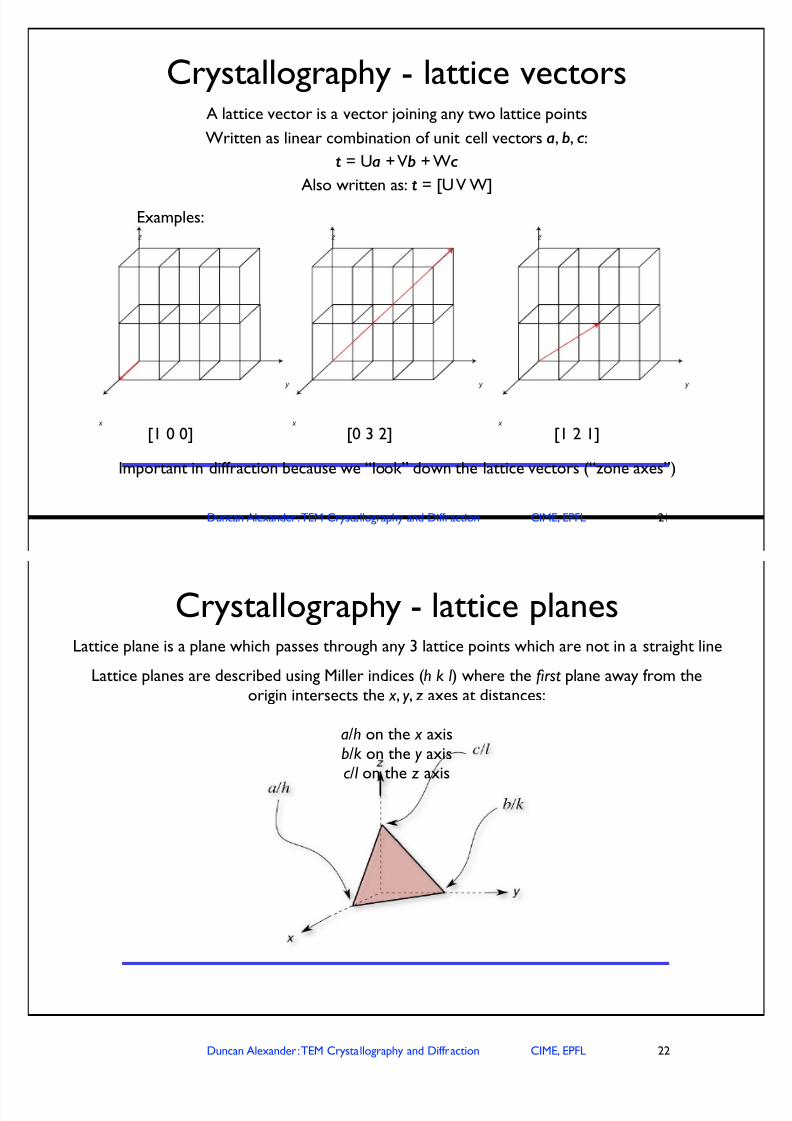
A lattice vector is a vector joining any two lattice points
Written as linear combination of unit cell vectors a, b, c:
t = Ua + Vb + Wc
Also written as: t = [U V W]
Examples: z
x
y
z
x
y
z
x
y
[1 0 0] [0 3 2] [1 2 1]
Important in diffraction because we “look” down the lattice vectors (“zone axes”)
Crystallography - lattice vectors
21
Duncan Alexander : TEM Crystallography and Diffraction CIME, EPFL
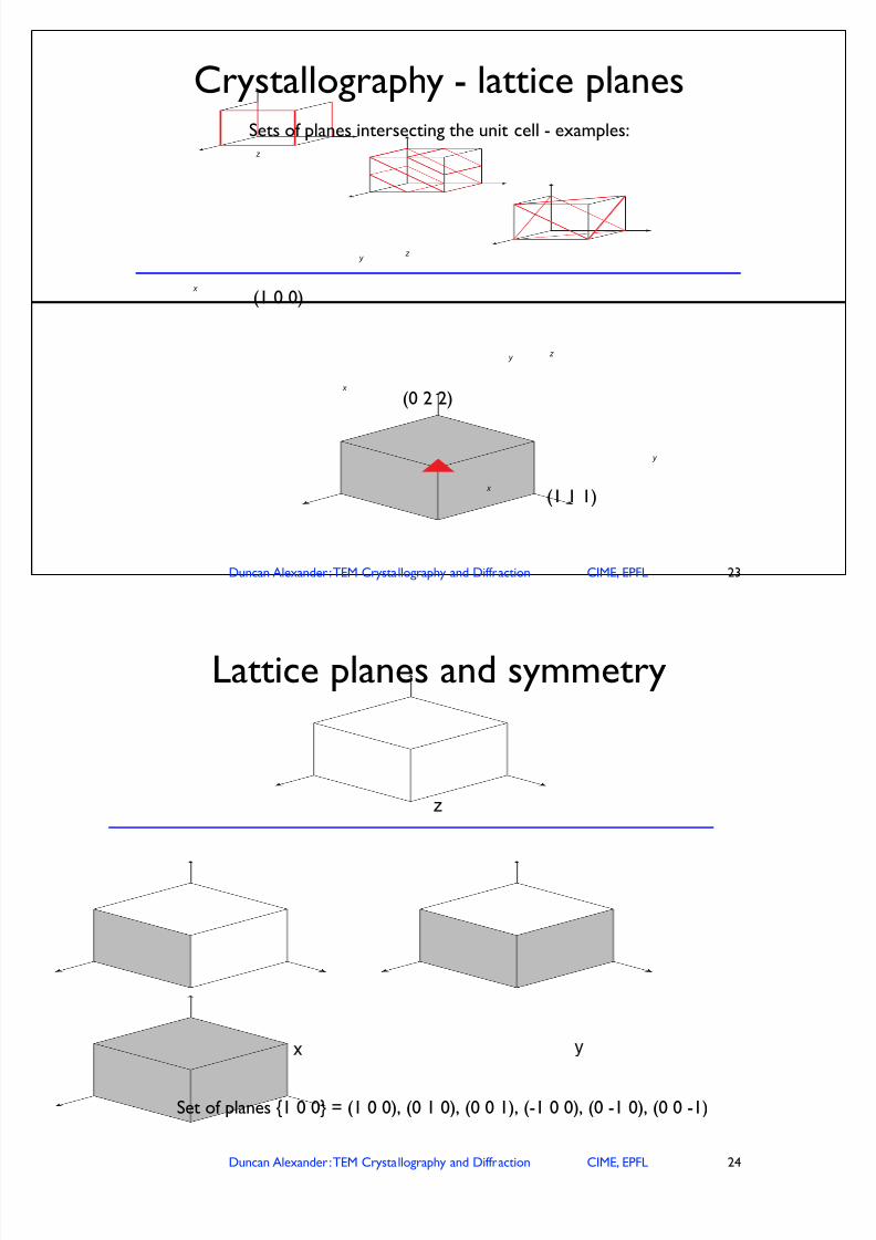
Lattice plane is a plane which passes through any 3 lattice points which are not in a straight line
Lattice planes are described using Miller indices (h k l ) where the first plane away from theorigin intersects the x , y , z axes at distances:
a/h on the x axis b/k on the y axis c /l on the z axis
Crystallography - lattice planes
22
7/18/2019 Chapter 3 and 4 TEM Crystallography and Diffraction
http://slidepdf.com/reader/full/chapter-3-and-4-tem-crystallography-and-diffraction 12/29
Duncan Alexander : TEM Crystallography and Diffraction CIME, EPFL
Sets of planes intersecting the unit cell - examples:
x
z
y
x
z
y
x
z
y
(1 0 0)
(0 2 2)
(1 1 1)
Crystallography - lattice planes
23
Duncan Alexander : TEM Crystallography and Diffraction CIME, EPFL
Lattice planes in a crystal related by the crystal symmetry
For example, in cubic lattices the 3-fold rotation axis on the [1 1 1] body diagonalrelates the planes (1 0 0), (0 1 0), (0 0 1):
x y
z
x y
z
x y
z
x y
z
x y
z
Set of planes {1 0 0} = (1 0 0), (0 1 0), (0 0 1), (-1 0 0), (0 -1 0), (0 0 -1)
Lattice planes and symmetry
24
7/18/2019 Chapter 3 and 4 TEM Crystallography and Diffraction
http://slidepdf.com/reader/full/chapter-3-and-4-tem-crystallography-and-diffraction 13/29
Duncan Alexander : TEM Crystallography and Diffraction CIME, EPFL
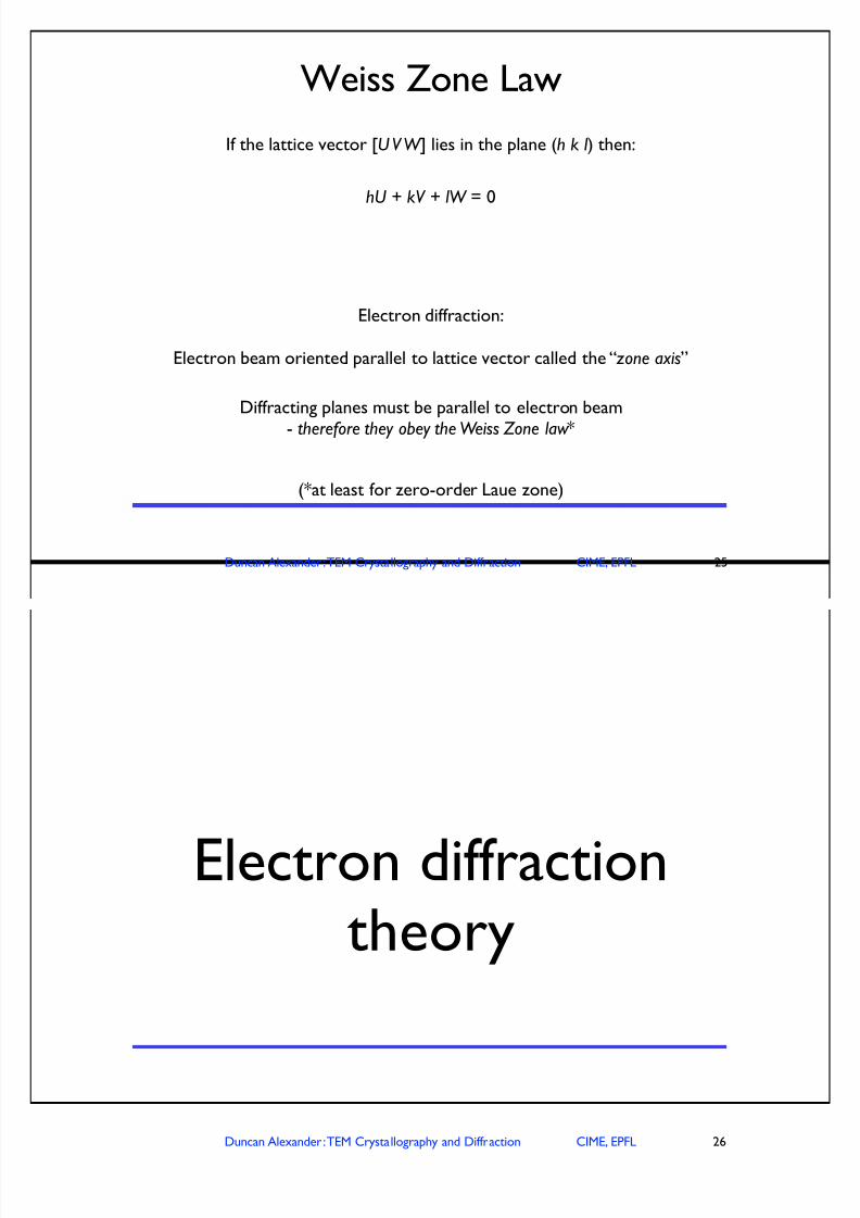
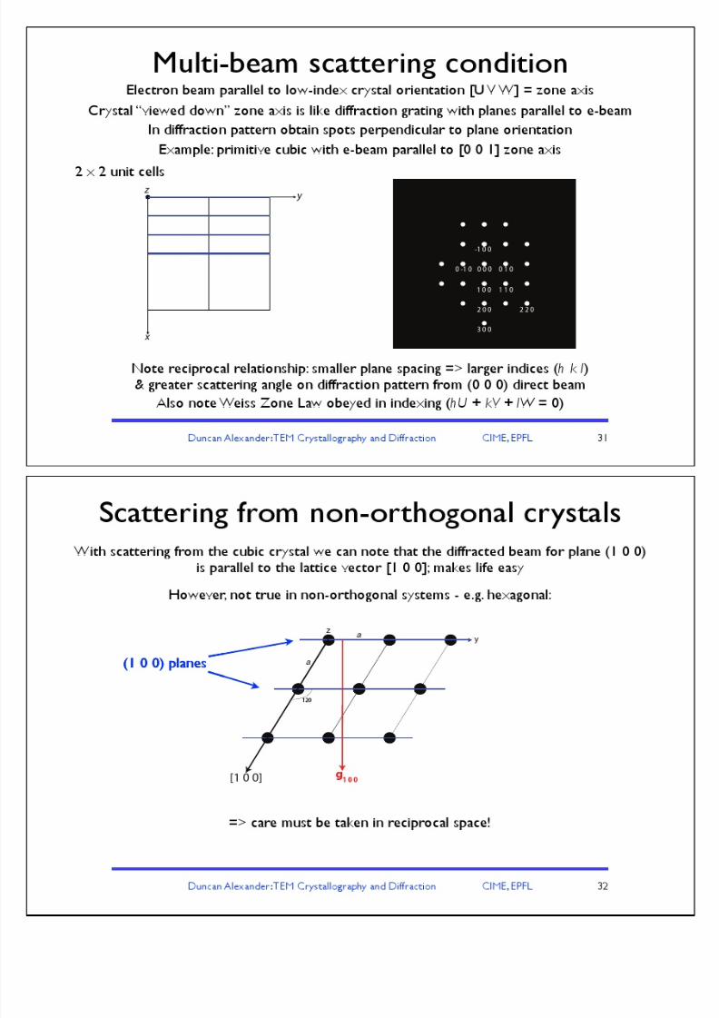
If the lattice vector [U V W ] lies in the plane (h k l ) then:
hU + kV + lW = 0
Electron diffraction:
Electron beam oriented parallel to lattice vector called the “ zone axis”
Diffracting planes must be parallel to electron beam
- therefore they obey the Weiss Zone law *
(*at least for zero-order Laue zone)
Weiss Zone Law
25
Duncan Alexander : TEM Crystallography and Diffraction CIME, EPFL
Electron diffractiontheory
26
7/18/2019 Chapter 3 and 4 TEM Crystallography and Diffraction
http://slidepdf.com/reader/full/chapter-3-and-4-tem-crystallography-and-diffraction 14/29
Duncan Alexander : TEM Crystallography and Diffraction CIME, EPFL 27
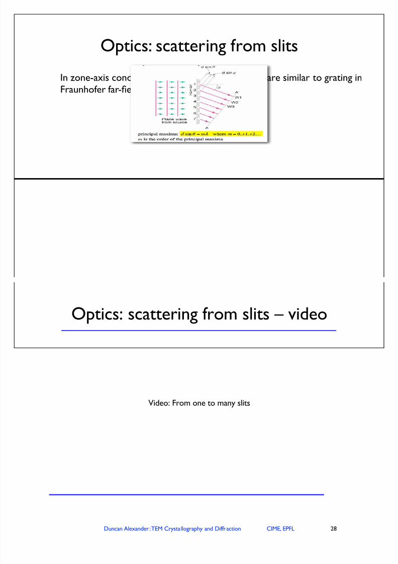
Optics: scattering from slits
In zone-axis condition our TEM optics and sample are similar to grating inFraunhofer far-field diffraction geometry
Incident plane wave (far-field) on diffraction grating => Periodic array of spots in diffraction plane
Duncan Alexander : TEM Crystallography and Diffraction CIME, EPFL 28
Video: From one to many slits
Optics: scattering from slits – video
7/18/2019 Chapter 3 and 4 TEM Crystallography and Diffraction
http://slidepdf.com/reader/full/chapter-3-and-4-tem-crystallography-and-diffraction 15/29
Duncan Alexander : TEM Crystallography and Diffraction CIME, EPFL
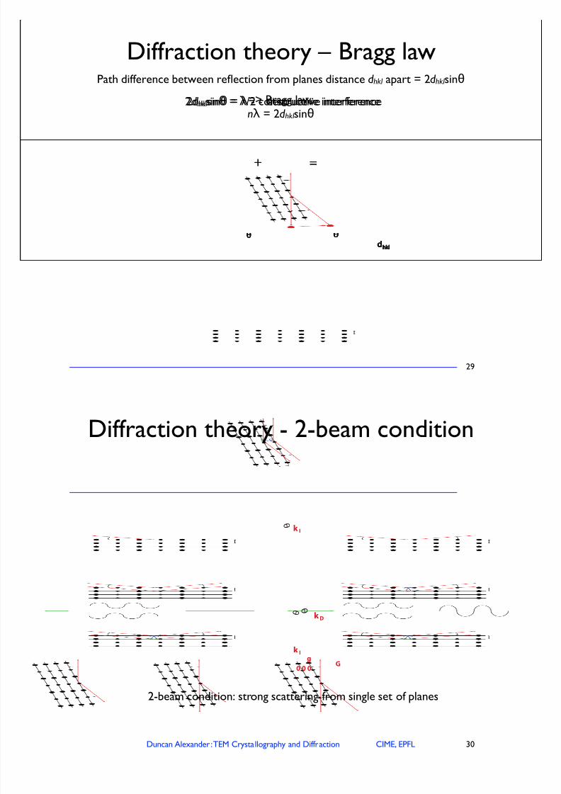
Path difference between reflection from planes distance d hkl apart = 2d hkl sin'
Electron diffraction: " ~ 0.001 nm therefore: " " d hkl
=> small angle approximation: n" ( 2d hkl '
Reciprocity: scattering angle ' # d hkl -1
dhkl
d
θ
hkld
θ θ
hkld
θ θ
hkld
θ θ
hkld
θ θ
+ =
hkld
θ θ
+ =
hkl
2d hkl sin' = "/2 - destructive interference2d hkl sin' = " - constructive interference=> Bragg law: n" = 2d hkl sin'
Diffraction theory – Bragg law
29
Duncan Alexander : TEM Crystallography and Diffraction CIME, EPFL
d
θ
θ
h k l
θ
θ
θ
θ θ
k I
θ
θ θ
k I
k D
k I
θ
θ
0 0 0G
g
θ
k I
k D
k I
2-beam condition: strong scattering from single set of planes
Diffraction theory - 2-beam condition
30
7/18/2019 Chapter 3 and 4 TEM Crystallography and Diffraction
http://slidepdf.com/reader/full/chapter-3-and-4-tem-crystallography-and-diffraction 16/29
7/18/2019 Chapter 3 and 4 TEM Crystallography and Diffraction
http://slidepdf.com/reader/full/chapter-3-and-4-tem-crystallography-and-diffraction 17/29
Duncan Alexander : TEM Crystallography and Diffraction CIME, EPFL
Diffraction as Fourier Transform
33
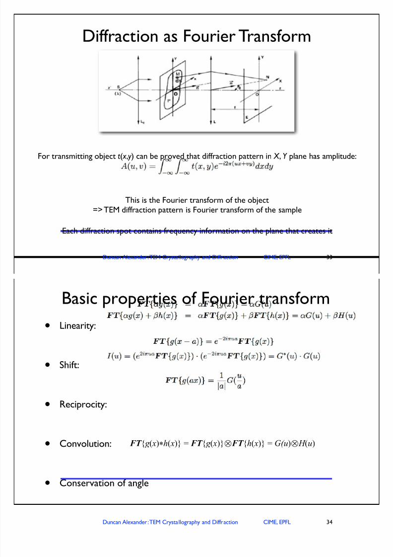
For transmitting object t( x , y ) can be proved that diffraction pattern in X , Y plane has amplitude:
This is the Fourier transform of the object=> TEM diffraction pattern is Fourier transform of the sample
Each diffraction spot contains frequency information on the plane that creates it
Duncan Alexander : TEM Crystallography and Diffraction CIME, EPFL
Basic properties of Fourier transform
• Linearity:
• Shift:
• Reciprocity:
• Convolution:
• Conservation of angle
34
FT { g ( x)*h( x)} = FT { g ( x)}$FT {h( x)} = G(u)$ H (u)
7/18/2019 Chapter 3 and 4 TEM Crystallography and Diffraction
http://slidepdf.com/reader/full/chapter-3-and-4-tem-crystallography-and-diffraction 18/29
Duncan Alexander : TEM Crystallography and Diffraction CIME, EPFL
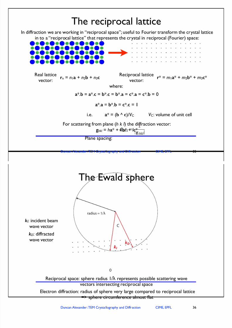
For scattering from plane (h k l ) the diffraction vector: ghkl = ha* + kb* + l c*
rn = n1a + n2b + n3cReal lattice
vector:
In diffraction we are working in “reciprocal space”; useful to Fourier transform the crystal latticein to a “reciprocal lattice” that represents the crystal in reciprocal (Fourier) space:
r* = m1a* + m2b* + m3c*Reciprocal lattice
vector:
a*.b = a*.c = b*.c = b*.a = c*.a = c*.b = 0
a*.a = b*.b = c*.c = 1
a* = (b ^ c)/V C
where:
i.e. V C: volume of unit cell
Plane spacing:
The reciprocal lattice
35
Duncan Alexander : TEM Crystallography and Diffraction CIME, EPFL
radius = 1/λ
0
k I
k D
C
Reciprocal space: sphere radius 1/" represents possible scattering wavevectors intersecting reciprocal space
kI: incident beamwave vector
kD: diffractedwave vector
Electron diffraction: radius of sphere very large compared to reciprocal lattice=> sphere circumference almost flat
The Ewald sphere
36
7/18/2019 Chapter 3 and 4 TEM Crystallography and Diffraction
http://slidepdf.com/reader/full/chapter-3-and-4-tem-crystallography-and-diffraction 19/29
Duncan Alexander : TEM Crystallography and Diffraction CIME, EPFL
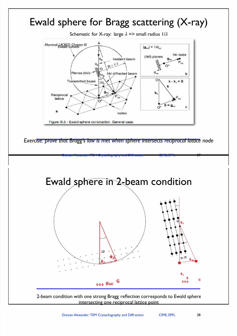
Ewald sphere for Bragg scattering (X-ray)
37
Schematic for X-ray: large ! => small radius 1/!
Morniroli LACBED Chapter III
Exercise: prove that Bragg’s law is met when sphere intersects reciprocal lattice node
Duncan Alexander : TEM Crystallography and Diffraction CIME, EPFL
k I
k D
ghkl
k k
G0 0 0
2θ
θ
θ
0 0 0G
g
θ
k I
k D
k I
2-beam condition with one strong Bragg reflection corresponds to Ewald sphereintersecting one reciprocal lattice point
Ewald sphere in 2-beam condition
38
7/18/2019 Chapter 3 and 4 TEM Crystallography and Diffraction
http://slidepdf.com/reader/full/chapter-3-and-4-tem-crystallography-and-diffraction 20/29
Duncan Alexander : TEM Crystallography and Diffraction CIME, EPFL
0 0 0
k I
k Dk k
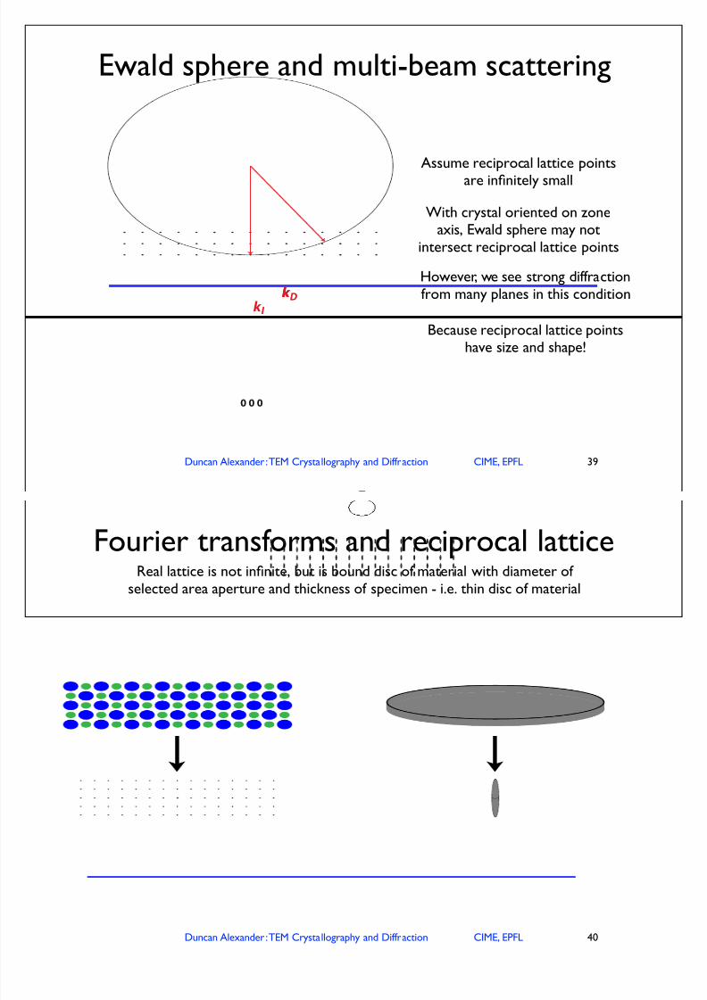
With crystal oriented on zoneaxis, Ewald sphere may not
intersect reciprocal lattice points
However, we see strong diffraction from many planes in this condition
Assume reciprocal lattice points
are infinitely small
Because reciprocal lattice points
have size and shape!
Ewald sphere and multi-beam scattering
39
Duncan Alexander : TEM Crystallography and Diffraction CIME, EPFL
Real lattice is not infinite, but is bound disc of material with diameter of selected area aperture and thickness of specimen - i.e. thin disc of material
X
FT FT
X “Relrod”
=2 lengths scales in reciprocal space!
Fourier transforms and reciprocal lattice
40
7/18/2019 Chapter 3 and 4 TEM Crystallography and Diffraction
http://slidepdf.com/reader/full/chapter-3-and-4-tem-crystallography-and-diffraction 21/29
Duncan Alexander : TEM Crystallography and Diffraction CIME, EPFL
0 0 0
k I
k Dk k
0 0 0
k I
k Dk k
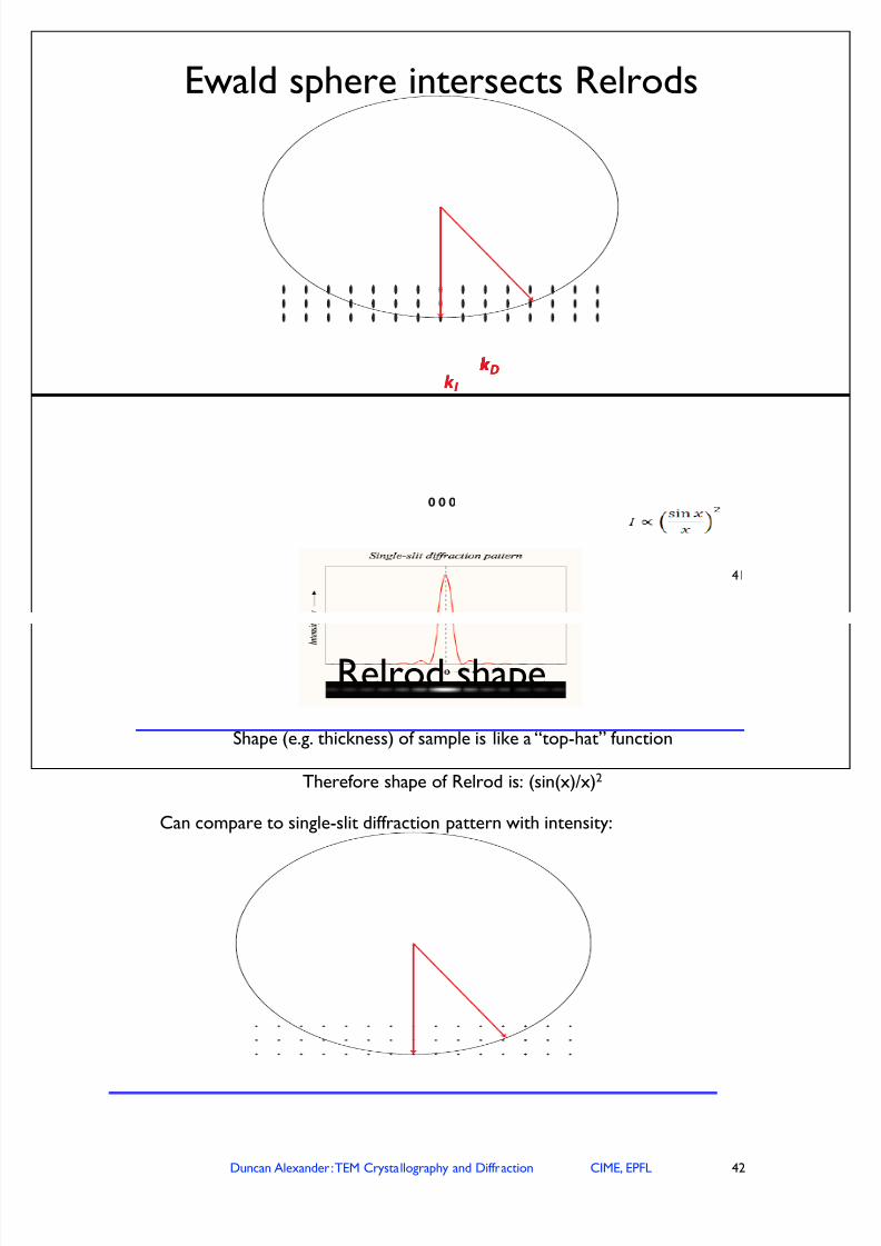
Ewald sphere intersects Relrods
41
Duncan Alexander : TEM Crystallography and Diffraction CIME, EPFL
Shape (e.g. thickness) of sample is like a “top-hat” function
Therefore shape of Relrod is: (sin(x)/x)2
Can compare to single-slit diffraction pattern with intensity:
Relrod shape
42
7/18/2019 Chapter 3 and 4 TEM Crystallography and Diffraction
http://slidepdf.com/reader/full/chapter-3-and-4-tem-crystallography-and-diffraction 22/29
Duncan Alexander : TEM Crystallography and Diffraction CIME, EPFL
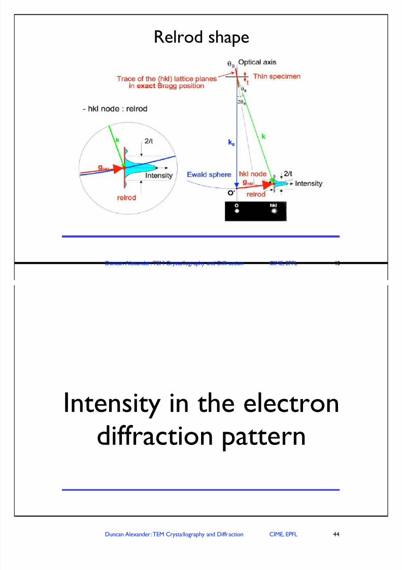
Relrod shape
43
Duncan Alexander : TEM Crystallography and Diffraction CIME, EPFL
Intensity in the electrondiffraction pattern
44
7/18/2019 Chapter 3 and 4 TEM Crystallography and Diffraction
http://slidepdf.com/reader/full/chapter-3-and-4-tem-crystallography-and-diffraction 23/29
Duncan Alexander : TEM Crystallography and Diffraction CIME, EPFL
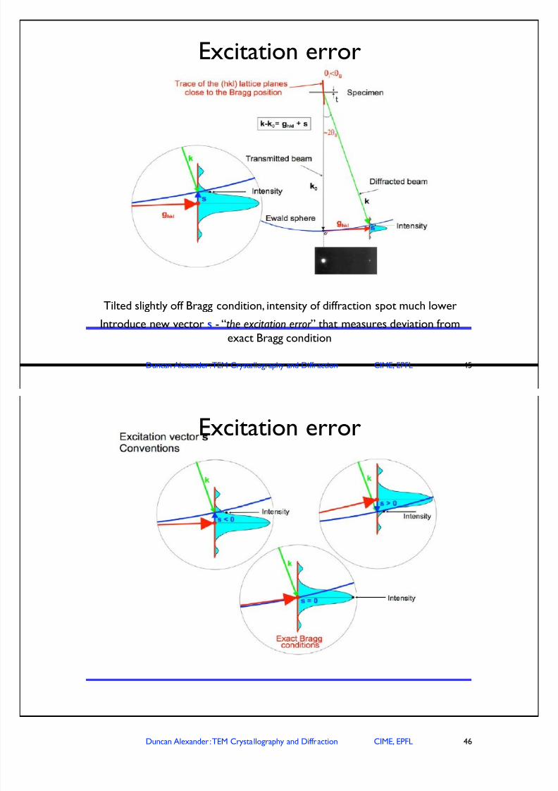
Tilted slightly off Bragg condition, intensity of diffraction spot much lower
Introduce new vector s - “the excitation error ” that measures deviation from exact Bragg condition
Excitation error
45
Duncan Alexander : TEM Crystallography and Diffraction CIME, EPFL
Excitation error
46
7/18/2019 Chapter 3 and 4 TEM Crystallography and Diffraction
http://slidepdf.com/reader/full/chapter-3-and-4-tem-crystallography-and-diffraction 24/29
Duncan Alexander : TEM Crystallography and Diffraction CIME, EPFL
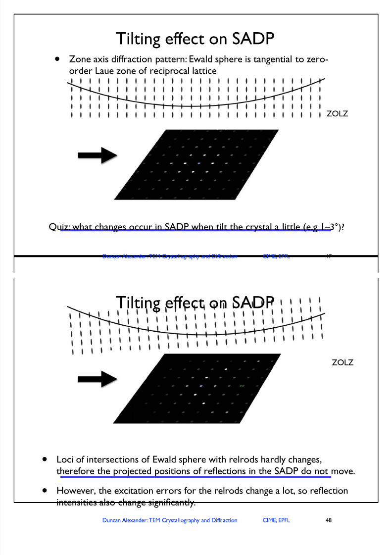
Tilting effect on SADP• Zone axis diffraction pattern: Ewald sphere is tangential to zero-
order Laue zone of reciprocal lattice
Quiz: what changes occur in SADP when tilt the crystal a little (e.g 1 –3°)?
ZOLZ
47
Duncan Alexander : TEM Crystallography and Diffraction CIME, EPFL
Tilting effect on SADP
ZOLZ
• Loci of intersections of Ewald sphere with relrods hardly changes,therefore the projected positions of reflections in the SADP do not move.
• However, the excitation errors for the relrods change a lot, so reflectionintensities also change significantly.
48
7/18/2019 Chapter 3 and 4 TEM Crystallography and Diffraction
http://slidepdf.com/reader/full/chapter-3-and-4-tem-crystallography-and-diffraction 25/29
Duncan Alexander : TEM Crystallography and Diffraction CIME, EPFL
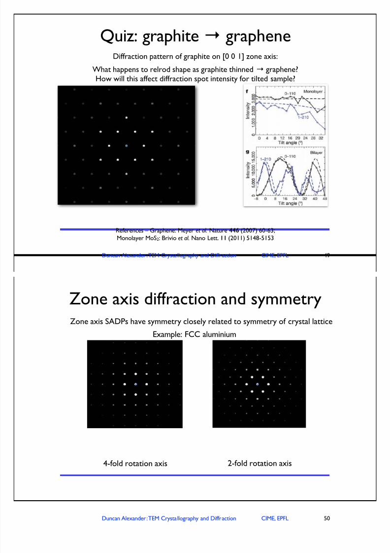
Quiz: graphite ) graphene
49
Diffraction pattern of graphite on [0 0 1] zone axis:
References – Graphene: Meyer et al. Nature 446 (2007) 60-63;
Monolayer MoS2: Brivio et al. Nano Lett. 11 (2011) 5148-5153
What happens to relrod shape as graphite thinned ) graphene? How will this affect diffraction spot intensity for tilted sample?
Duncan Alexander : TEM Crystallography and Diffraction CIME, EPFL
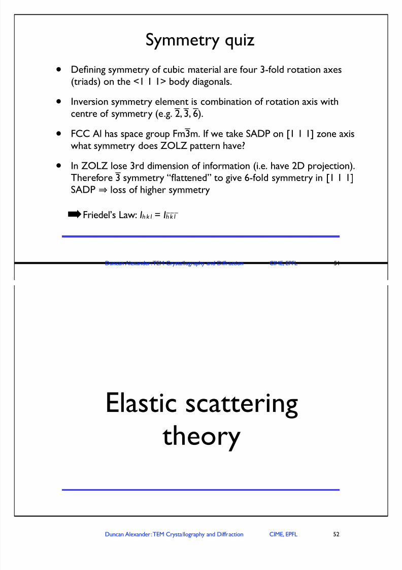
Zone axis diffraction and symmetry
50
Zone axis SADPs have symmetry closely related to symmetry of crystal lattice
Example: FCC aluminium
[0 0 1] [1 1 0]
4-fold rotation axis 2-fold rotation axis
7/18/2019 Chapter 3 and 4 TEM Crystallography and Diffraction
http://slidepdf.com/reader/full/chapter-3-and-4-tem-crystallography-and-diffraction 26/29
Duncan Alexander : TEM Crystallography and Diffraction CIME, EPFL
Symmetry quiz
• Defining symmetry of cubic material are four 3-fold rotation axes(triads) on the <1 1 1> body diagonals.
• Inversion symmetry element is combination of rotation axis withcentre of symmetry (e.g. 2, 3, 6).
• FCC Al has space group Fm3m. If we take SADP on [1 1 1] zone axiswhat symmetry does ZOLZ pattern have?
• In ZOLZ lose 3rd dimension of information (i.e. have 2D projection).Therefore 3 symmetry “flattened” to give 6-fold symmetry in [1 1 1]SADP loss of higher symmetry
#Friedel’s Law: Ih k l = Ih k l
51
– – –
–
–––
–
Duncan Alexander : TEM Crystallography and Diffraction CIME, EPFL
Elastic scatteringtheory
52
7/18/2019 Chapter 3 and 4 TEM Crystallography and Diffraction
http://slidepdf.com/reader/full/chapter-3-and-4-tem-crystallography-and-diffraction 27/29
Duncan Alexander : TEM Crystallography and Diffraction CIME, EPFL
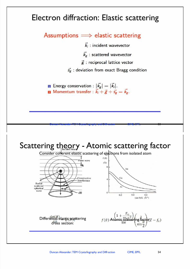
Electron diffraction: Elastic scattering
53
Duncan Alexander : TEM Crystallography and Diffraction CIME, EPFL
Consider coherent elastic scattering of electrons from isolated atom
Differential elastic scattering cross section:
Atomic scattering factor
Scattering theory - Atomic scattering factor
54
7/18/2019 Chapter 3 and 4 TEM Crystallography and Diffraction
http://slidepdf.com/reader/full/chapter-3-and-4-tem-crystallography-and-diffraction 28/29
Duncan Alexander : TEM Crystallography and Diffraction CIME, EPFL
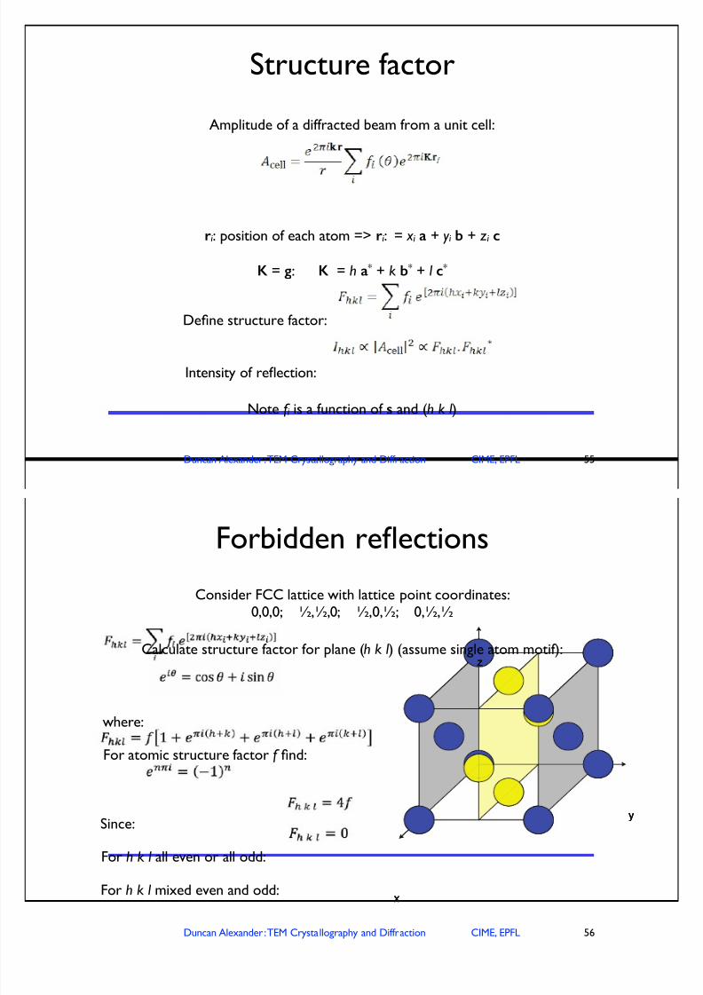
Amplitude of a diffracted beam from a unit cell:
ri : position of each atom => ri : = x i a + y i b + zi c
K = g: K = h a* + k b* + l c*
Define structure factor:
Intensity of reflection:
Structure factor
55
Note f i is a function of s and (h k l )
Duncan Alexander : TEM Crystallography and Diffraction CIME, EPFL
Consider FCC lattice with lattice point coordinates: 0,0,0; ",",0; ",0,"; 0,","
x
z
y
Calculate structure factor for plane (h k l ) (assume single atom motif):
x
z
y
x
z
y
x
z
y
Forbidden reflections
56
where:
For atomic structure factor f find:
Since:
For h k l all even or all odd:
For h k l mixed even and odd:
7/18/2019 Chapter 3 and 4 TEM Crystallography and Diffraction
http://slidepdf.com/reader/full/chapter-3-and-4-tem-crystallography-and-diffraction 29/29
Duncan Alexander : TEM Crystallography and Diffraction CIME, EPFL
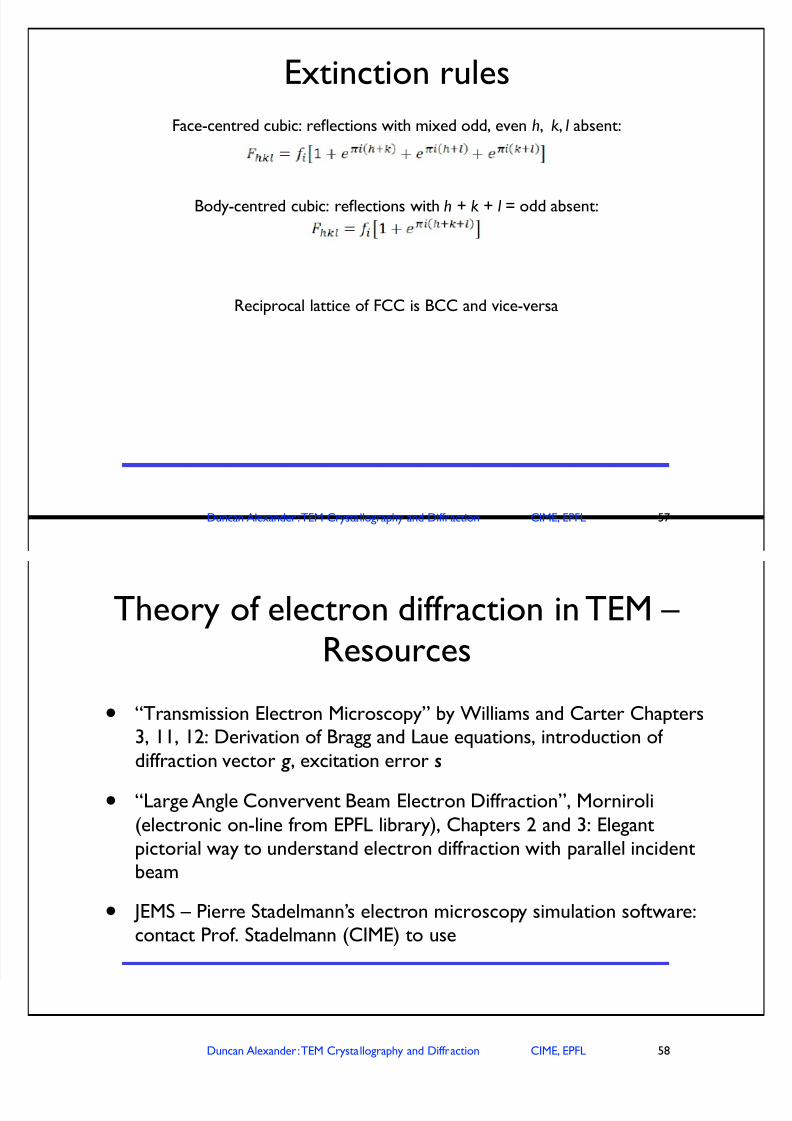
Reciprocal lattice of FCC is BCC and vice-versa
Extinction rules
57
Face-centred cubic: reflections with mixed odd, even h, k, l absent:
Body-centred cubic: reflections with h + k + l = odd absent:
Theory of electron diffraction in TEM – Resources
• “Transmission Electron Microscopy” by Williams and Carter Chapters3, 11, 12: Derivation of Bragg and Laue equations, introduction ofdiffraction vector g , excitation error s
• “Large Angle Convervent Beam Electron Diffraction”, Morniroli(electronic on-line from EPFL library), Chapters 2 and 3: Elegantpictorial way to understand electron diffraction with parallel incidentbeam
• JEMS – Pierre Stadelmann’s electron microscopy simulation software:contact Prof. Stadelmann (CIME) to use