Embed Size (px)
Citation preview
Sains Malaysiana 46(7)(2017): 1103–1109 http://dx.doi.org/10.17576/jsm-2017-4607-13
Characterization of Transparent Conducting Carbon Nanotube Thin Films Prepared via Different Methods
(Pencirian Filem Nipis Pengalir Lutsinar Tiub Nano Karbon Disediakan Melalui Pelbagai Kaedah)
ISKANDAR YAHYA*, LEE LI THENG, SERI MASTURA MUSTAZA, HUDA ABDULLAH & NOWSHAD AMIN
ABSTRACT
The fabrication and characterization of transparent conductors based on single walled carbon nanotube (SWCNT) thin films were carried out in controlled environment and its performance compared. Here, we demonstrate the fabrication of thin, transparent, optically homogeneous, electrically conducting films of metallic enriched single-walled carbon nanotubes via three different deposition techniques namely dip coating, vacuum filtration and Langmuir Blodgett. Optical characterization showed that the maximum transmittance, TM, in Vis region is ~ 96.3% and minimum surface roughness, Ra ~ 4.87 nm achieved via Langmuir-Blodgett technique. I-V characteristics shows minimum sheet resistance, Rs ~ 3.62 × 10³ Ω/sq and maximum conductivity, σ ~ 27.65 Ω-1cm-1 for vacuum filtration technique. It is shown that SWCNT deposition technique significantly affects the optical and electrical characteristics of resulting thin films. Langmuir Blodgett method produced film with the lowest surface roughness of Ra ~ 4.87 nm and uniform conductivity of σ ~ 0.025 Ω-1cm-1, whereas vacuum filtration method produced film with the highest surface roughness of Ra ~ 12.83 nm and non-uniform conductivity, σ, ranging from ~ 0.199 to ~0.017 Ω-1cm-1 depending on the film dimensions.
Keywords: Single walled carbon nanotubes; thin films; transparent conductor
ABSTRAK
Fabrikasi dan pencirian pengalir lutsinar berdasarkan filem nipis tiub nano karbon dinding tunggal (SWCNT) telah dijalankan dalam persekitaran terkawal dan perbandingan prestasinya dibuat. Di sini, kita menunjukkan fabrikasi filem nipis, telus, homogen dan bersifat konduksi elektrik daripada karbon tiub nano dinding tunggal yang diperkaya secara metalik melalui tiga teknik pemendapan yang berbeza iaitu celup salutan, penapisan vakum dan Langmuir-Blodgett. Pencirian optik menunjukkan bahawa pemindahan maksimum, TM, bagi gelombang Vis adalah ~ 96.3% dan kekasaran permukaan minimum, Ra adalah ~ 4.87 nm dicapai melalui teknik Langmuir-Blodgett. Pencirian I-V menunjukkan rintangan helaian, Rs ~ 3.62 × 10³ Ω/sq dan kekonduksian maksima, σ ~ 27.65 Ω-1cm-1 melalui teknik penapisan vakum. Ditunjukkan bahawa teknik pemendapan SWCNT memberi kesan yang signifikan terhadap ciri optik dan elektrik filem nipis yang dihasilkan. Teknik Langmuir Blodgett menghasilkan filem nipis dengan kekasaran permukaan terendah iaitu Ra ~ 4.87 nm dan kekonduksian yang sekata pada nilai σ ~ 0.025 Ω-1cm-1, manakala teknik penapisan vakum menghasilkan filem nipis dengan kekasaran permukaan tertinggi iaitu Ra ~ 12.83 nm dan kekonduksian, σ, yang tidak sekata pada julat ~ 0.199 to ~0.017 Ω-1cm-1, bergantung kepada dimensi filem.
Kata kunci: Filem nipis; karbon tiub nano dinding tunggal; konduktor telus
INTRODUCTION
Carbon nanotubes (CNTs) are high aspect ratio conducting nanomaterials that demonstrate excellent optical and electronic properties. They are ideal building blocks for use in assembling a randomly oriented, highly connected nano-porous and thin continuous network. Single-walled carbon nanotubes (SWCNTs) exhibit metallic or semiconducting electronic properties depending on the chirality (Jorio et al. 2008). When a network of separated metallic SWCNTs is deposited on top of a substrate forming a thin film with thickness in the range of 10-250 nm, it behaves as a transparent conducting film; an important material for many electronic device applications, currently dominated by tin-doped indium oxide (ITO) (Mizuhashi 1980).
The demand for transparent conductors is expected to grow rapidly as electronic devices, such as displays, solar cells and touch screens become more interactive and ubiquitous. However, commonly used transparent conductor materials such as Indium tin oxide (ITO) are scares, expensive, brittle and suffers from thermal degradation. Therefore, there is a need for cheaper and higher performance alternative materials. Such a material is carbon nanotube thin films, which have shown much potential as high performance transparent conductor. However, the fabrication of SWCNT thin films are not straight forward due to several challenges. Firstly, synthesized SWCNTs statistically contains a mixture of both metallic and semiconducting SWCNTs; although it has been
1104
shown that controlling the growth selectivity either metallic (Zhao et al. 2012) or semiconducting (Li et al. 2014) enriched is possible, albeit not 100%. In order to produce a SWCNT thin film with maximum conductivity requires pure metallic SWCNTs, and to date, the most practical and scalable method to obtain it is by post-synthesis separation via solution based processes, which adds complexity to the overall thin film fabrication. Secondly, direct growth of metallic enriched SWCNT transparent thin films is possible but only limited to using quartz substrate (Ding et al. 2008). Therefore, there is a need for an added step to transfer the films to other transparent substrates such as glass, plastics and polymers. The simplest route to produce transparent conducting SWCNT thin films is by using solution-based processed SWCNTs via several deposition techniques for producing uniform and thin conducting layer. Three of the techniques already explored are dip-coating (DP) (Ko et al. 2014), vacuum filtration (VF) (Wu 2004) and Langmuir-Blodgett (LB) (Kim et al. 2003). Each of the three techniques is unique in terms of the inherent trade-off between complexity of the method and performance of the resulting films. Therefore, there is a need for a comparative study to investigate the characteristics and performance of the transparent conducting SWCNT thin films fabricated using the aforementioned techniques. Here, we demonstrate the fabrication of transparent conducting SWCNT thin films using DP, VF and LB techniques with a common SWCNT source and controlled environment. The optical and electrical characterization of the fabricated thin films are compared and reported.
MATERIALS AND METHODS
The SWCNTs source used were obtained from Nikkisso Japan Corp synthesized by chemical vapor deposition (CVD) enhanced with direct injection pyrolytic (Ago et al. 2001) with average tube diameter and range of 2.0 nm and 0.8 - 3.0 nm, respectively. The tube lengths are between 1- 10 μm. The as-received SWCNT carbon soot were purified and subjected to post-synthesis separation via temperature controlled gel-agarose chromatography filtration technique to obtain metallic enriched SWCNTs. We have reported the detailed methods for purification and separation previously elsewhere (Yahya et al. 2015). From comprehensive resonance Raman scattering (RRS) spectroscopy analysis, the purity of the metallic enriched SWCNTs was estimated to be ~ 70%, which is higher than that of as prepared samples with metallic SWCNT population of ~ 30% (Yahya et al. 2015). The metallic SWCNTs enriched portion of the separation yield solution were vacuum filtered using mixed cellulose esters membrane filters with pore size of ~ 0.22 μm to remove the solvent and surfactants. These filtered metallic SWCNTs enriched tubes were then dispersed in two different solvents depending on the thin film deposition techniques described here. For dip-coating (DC) deposition technique, the SWCNTs dispersions are prepared by adding 1 mg/10 mL
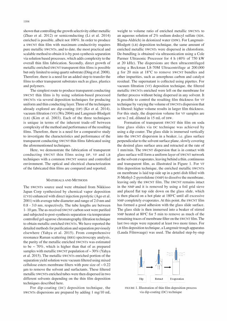
weight to volume ratio of enriched metallic SWCNTs to an aqueous solution of 2% sodium dodecyl sulfate (SDS, Sigma-Aldrich) in deionized water (DIW). For Langmuir-Blodgett (LB) deposition technique, the same amount of enriched metallic SWCNTs were dispersed in chloroform. De-bundling is obtained via ultrasonication using a Cole Parmer Ultrasonic Processor for 4 h (40% of 750 kW at 20 kHz). The dispersions are then ultracentrifuged using a Beckman L8-70M Ultracentrifuge at 200,000 g for 20 min at 18°C to remove SWCNT bundles and other impurities, such as amorphous carbon and catalyst residual. The supernatant is collected using pipettes. For vacuum filtration (VF) deposition technique, the filtered metallic SWCNTs enriched were left on the membrane for further process without being dispersed in any solvent. It is possible to control the resulting film thickness for VF technique by varying the volume of SWCNTs dispersion that is filtered; higher volume results in larger film thickness. For this study, the dispersion volume for VF samples are set to 2 mL diluted in 15 mL of DIW. Formation of transparent SWCNT thin film on soda lime glass slides via DC technique was achieved by using a dip coater. The glass slide is immersed vertically into the SWCNT dispersion in a beaker, i.e. glass surface perpendicular to the solvent surface plane, slowly covering the desired glass surface area and retracted at the rate of 1 mm/min. The SWCNT dispersion that is in contact with glass surface will form a uniform layer of SWCNT network as the solvent evaporates, leaving behind a thin, continuous and transparent film, as illustrated in Figure 1. For VF film deposition technique, the enriched metallic SWCNTs on membrane is laid top side up in a petri dish filled with N-Methyl-2-pyrrolidone (NMP) to dissolve the membrane, leaving only the SWCNT film. The SWCNT remains intact in the NMP and it is removed by using a foil grid sieve and placed flat top side down on the glass slide, which is then placed on a hot plate at 180oC until all excessive NMP completely evaporates. At this point, the SWCNT film has formed a good adhesion with the glass slide surface. The glass slide is then immersed into a beaker of stirred NMP heated at 80oC for 5 min to remove as much of the remaining traces of membrane filter on the SWCNT film. The last two steps were repeated at least two more times. For LB film deposition technique, a Langmuir trough apparatus (Lauda Filmwaage) was used. The detailed step-by-step
FIGURE 1. Illustration of thin film deposition process via dip-coating (DC) technique
1105
description of the process is based on a previous report (Kim et al. 2003). Several optical and electrical characterizations tools were used to obtain the key parameters. Scanning electron microscopy (SEM) was done using Hitachi S3400N at 15 kV to inspect qualitatively the homogeneity and continuity of the thin films. Atomic force microscopy (AFM) was done using AFM-Solver NEXT (NT-MDT) to estimate the surface roughness and film thickness by measuring the step size between thin film edge and glass surface. Vis optical absorption spectroscopy at source wavelength of 390 - 700 nm using Varian Cary 5000 was carried out to estimate the transmittance of the transparent film within the visible light wavelength range. Two terminal I-V electrical measurement was done using Keithley 4200 analyzer to estimate the resistivity, ρ, conductivity, σ and sheet resistance, Rs.
RESULTS AND DISCUSSION
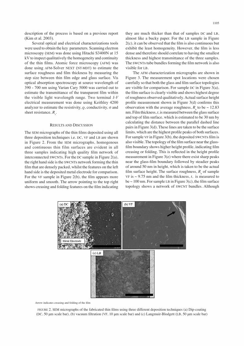
The SEM micrographs of the thin films deposited using all three deposition techniques i.e. DC, VF and LB are shown in Figure 2. From the SEM micrographs, homogenous and continuous thin film surfaces are evident in all three samples indicating high quality film network of interconnected SWCNTs. For the DC sample in Figure 2(a), the right hand side is the SWCNTs network forming the thin film that are densely packed, whilst the features on the left hand side is the deposited metal electrode for comparison. For the VF sample in Figure 2(b), the film appears more uniform and smooth. The arrow pointing to the top right shows creasing and folding features on the film indicating
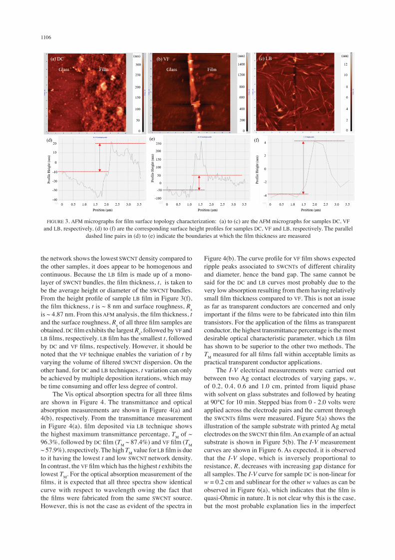
they are much thicker than that of samples DC and LB, almost like a bucky paper. For the LB sample in Figure 2(c), it can be observed that the film is also continuous but exhibit the least homogeneity. However, the film is less dense and therefore should correlate to having the smallest thickness and highest transmittance of the three samples. The SWCNTs tube bundles forming the film network is also visible for LB. The AFM characterization micrographs are shown in Figure 3. The measurement spot locations were chosen carefully so that both the glass and film surface topologies are visible for comparison. For sample DC in Figure 3(a), the film surface is clearly visible and shows highest degree of roughness observed qualitatively. Actual surface height profile measurement shown in Figure 3(d) confirms this observation with the average roughness, Ra to be ~ 12.83 nm. Film thickness, t, is measured between the glass surface and top of film surface, which is estimated to be 30 nm by calculating the distance between the parallel dashed line pairs in Figure 3(d). These lines are taken to be the surface limits, which are the highest profile peaks of both surfaces. For sample VF in Figure 3(b), the deposited SWCNTs film is also visible. The topology of the film surface near the glass-film boundary shows higher height profile, indicating film creasing or folding. This is reflected in the height profile measurement in Figure 3(e) where there exist sharp peaks near the glass-film boundary followed by steadier peaks of around 50 nm in height, which is taken to be the actual film surface height. The surface roughness, Ra of sample VF is ~ 9.75 nm and the film thickness, t, is measured to be ~ 100 nm. For sample LB in Figure 3(c), the film surface topology shows a network of SWCNT bundles. Although
Arrow indicates creasing and folding of the film
FIGURE 2. SEM micrographs of the fabricated thin films using three different deposition techniques (a) Dip-coating (DC, 50 μm scale bar), (b) vacuum filtration (VF, 10 μm scale bar) and (c) Langmuir-Blodgett (LB, 50 μm scale bar)
1106
the network shows the lowest SWCNT density compared to the other samples, it does appear to be homogenous and continuous. Because the LB film is made up of a mono-layer of SWCNT bundles, the film thickness, t, is taken to be the average height or diameter of the SWCNT bundles. From the height profile of sample LB film in Figure 3(f), the film thickness, t is ~ 8 nm and surface roughness, Ra is ~ 4.87 nm. From this AFM analysis, the film thickness, t and the surface roughness, Ra of all three film samples are obtained. DC film exhibits the largest Ra, followed by VF and LB films, respectively. LB film has the smallest t, followed by DC and VF films, respectively. However, it should be noted that the VF technique enables the variation of t by varying the volume of filtered SWCNT dispersion. On the other hand, for DC and LB techniques, t variation can only be achieved by multiple deposition iterations, which may be time consuming and offer less degree of control. The Vis optical absorption spectra for all three films are shown in Figure 4. The transmittance and optical absorption measurements are shown in Figure 4(a) and 4(b), respectively. From the transmittance measurement in Figure 4(a), film deposited via LB technique shows the highest maximum transmittance percentage, TM of ~ 96.3%, followed by DC film (TM ~ 87.4%) and VF film (TM ~ 57.9%), respectively. The high TM value for LB film is due to it having the lowest t and low SWCNT network density. In contrast, the VF film which has the highest t exhibits the lowest TM. For the optical absorption measurement of the films, it is expected that all three spectra show identical curve with respect to wavelength owing the fact that the films were fabricated from the same SWCNT source. However, this is not the case as evident of the spectra in
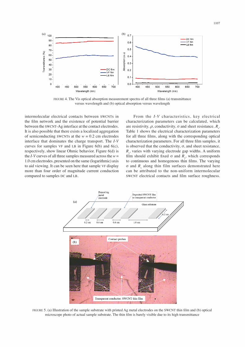
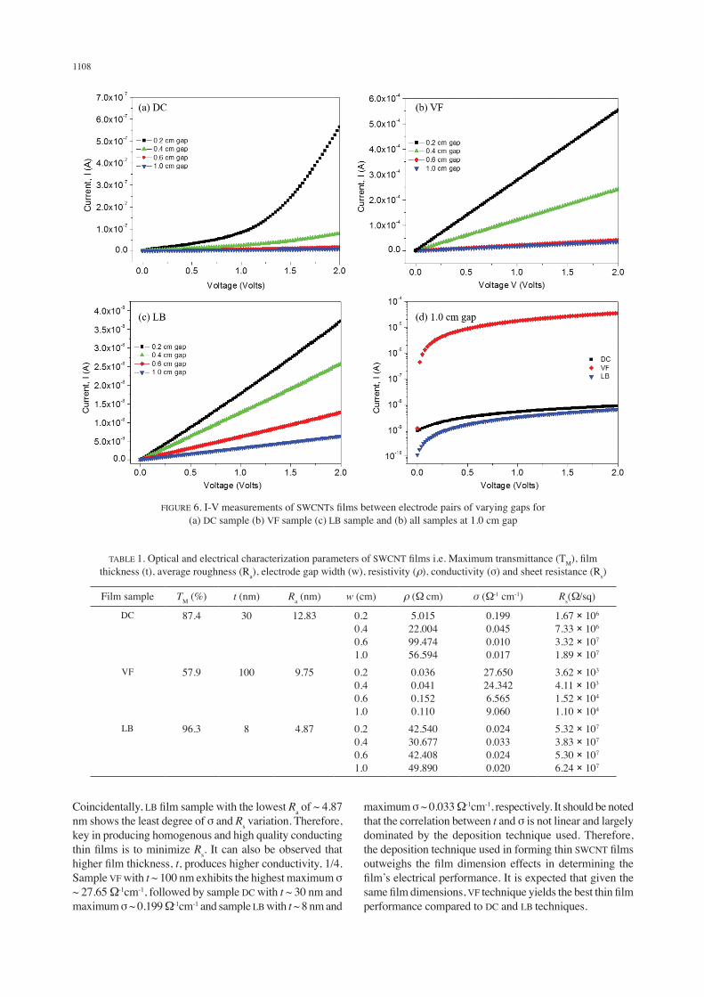
Figure 4(b). The curve profile for VF film shows expected ripple peaks associated to SWCNTs of different chirality and diameter, hence the band gap. The same cannot be said for the DC and LB curves most probably due to the very low absorption resulting from them having relatively small film thickness compared to VF. This is not an issue as far as transparent conductors are concerned and only important if the films were to be fabricated into thin film transistors. For the application of the films as transparent conductor, the highest transmittance percentage is the most desirable optical characteristic parameter, which LB film has shown to be superior to the other two methods. The TM measured for all films fall within acceptable limits as practical transparent conductor applications. The I-V electrical measurements were carried out between two Ag contact electrodes of varying gaps, w, of 0.2, 0.4, 0.6 and 1.0 cm, printed from liquid phase with solvent on glass substrates and followed by heating at 90°C for 10 min. Stepped bias from 0 - 2.0 volts were applied across the electrode pairs and the current through the SWCNTs films were measured. Figure 5(a) shows the illustration of the sample substrate with printed Ag metal electrodes on the SWCNT thin film. An example of an actual substrate is shown in Figure 5(b). The I-V measurement curves are shown in Figure 6. As expected, it is observed that the I-V slope, which is inversely proportional to resistance, R, decreases with increasing gap distance for all samples. The I-V curve for sample DC is non-linear for w = 0.2 cm and sublinear for the other w values as can be observed in Figure 6(a), which indicates that the film is quasi-Ohmic in nature. It is not clear why this is the case, but the most probable explanation lies in the imperfect
FIGURE 3. AFM micrographs for film surface topology characterization: (a) to (c) are the AFM micrographs for samples DC, VF and LB, respectively, (d) to (f) are the corresponding surface height profiles for samples DC, VF and LB, respectively. The parallel
dashed line pairs in (d) to (e) indicate the boundaries at which the film thickness are measured
1107
intermolecular electrical contacts between SWCNTs in the film network and the existence of potential barrier between the SWCNT-Ag interface at the contact electrodes. It is also possible that there exists a localized aggregation of semiconducting SWCNTs at the w = 0.2 cm electrodes interface that dominates the charge transport. The I-V curves for samples VF and LB in Figure 6(b) and 6(c), respectively, show linear Ohmic behavior. Figure 6(d) is the I-V curves of all three samples measured across the w = 1.0 cm electrodes, presented on the same (logarithmic) axis to aid viewing. It can be seen here that sample VF display more than four order of magnitude current conduction compared to samples DC and LB.
From the I-V characteristics, key electrical characterization parameters can be calculated, which are resistivity, ρ, conductivity, σ and sheet resistance, Rs. Table 1 shows the electrical characterization parameters for all three films, along with the corresponding optical characterization parameters. For all three film samples, it is observed that the conductivity, σ, and sheet resistance, Rs, varies with varying electrode gap widths. A uniform film should exhibit fixed σ and Rs, which corresponds to continuous and homogenous thin films. The varying σ and Rs along thin film surfaces demonstrated here can be attributed to the non-uniform intermolecular SWCNT electrical contacts and film surface roughness.
FIGURE 4. The Vis optical absorption measurement spectra of all three films (a) transmittance versus wavelength and (b) optical absorption versus wavelength
FIGURE 5. (a) Illustration of the sample substrate with printed Ag metal electrodes on the SWCNT thin film and (b) optical microscope photo of actual sample substrate. The thin film is barely visible due to its high transmittance
1108
FIGURE 6. I-V measurements of SWCNTs films between electrode pairs of varying gaps for (a) DC sample (b) VF sample (c) LB sample and (b) all samples at 1.0 cm gap
Coincidentally, LB film sample with the lowest Ra of ~ 4.87 nm shows the least degree of σ and Rs variation. Therefore, key in producing homogenous and high quality conducting thin films is to minimize Rs. It can also be observed that higher film thickness, t, produces higher conductivity, 1/4. Sample VF with t ~ 100 nm exhibits the highest maximum σ ~ 27.65 Ω-1cm-1, followed by sample DC with t ~ 30 nm and maximum σ ~ 0.199 Ω-1cm-1 and sample LB with t ~ 8 nm and
maximum σ ~ 0.033 Ω-1cm-1, respectively. It should be noted that the correlation between t and σ is not linear and largely dominated by the deposition technique used. Therefore, the deposition technique used in forming thin SWCNT films outweighs the film dimension effects in determining the film’s electrical performance. It is expected that given the same film dimensions, VF technique yields the best thin film performance compared to DC and LB techniques.
TABLE 1. Optical and electrical characterization parameters of SWCNT films i.e. Maximum transmittance (TM), film thickness (t), average roughness (Ra), electrode gap width (w), resistivity (ρ), conductivity (σ) and sheet resistance (Rs)
Film sample TM (%) t (nm) Ra (nm) w (cm) ρ (Ω cm) σ (Ω-1 cm-1) Rs(Ω/sq)
DC 87.4 30 12.83 0.20.40.61.0
5.01522.00499.47456.594
0.1990.0450.0100.017
1.67 × 10⁶
7.33 × 10⁶
3.32 × 10⁷
1.89 × 10⁷
VF 57.9 100 9.75 0.2 0.4 0.6 1.0
0.036 0.041 0.152 0.110
27.650 24.342 6.565 9.060
3.62 × 10³ 4.11 × 10³ 1.52 × 10⁴ 1.10 × 10⁴
LB 96.3 8 4.87 0.2 0.4 0.6 1.0
42.540 30.677 42.408 49.890
0.024 0.033 0.024 0.020
5.32 × 10⁷ 3.83 × 10⁷ 5.30 × 10⁷ 6.24 × 10⁷
1109
Overall, there are certain trade-offs between optical performance and electrical performance of SWCNT transparent thin films produced using different deposition techniques. From the results shown in Table 1, higher TM requires lower t at the expense of detrimentally lower electrical performance and vice versa. Finding the balance between optical and electrical performance will depends largely on the device application for optimum device operation. It is also shown here that high quality surface topology plays a significant role in determining the material and hence device performance. For large surface area applications such as display, SWCNT film deposition method that produces the lowest surface roughness, Ra, should be the main consideration because of its inherent factor, whilst the electrical performance can be improved by increasing film thickness.
CONCLUSION
We demonstrated the fabrication of transparent conductor thin films based on SWCNTs from common source using three different deposition techniques i.e. dip coating, vacuum filtration and Langmuir-Blodgett. The optical and electrical characteristics of the fabricated films have been investigated experimentally. The key finding in this work is that film surface topology qualities such as homogeneity and continuity depends on the deposition technique used, which in turn determines its electrical performance. Langmuir-Blodgett technique yields films with the best optical performance of TM ~ 96.3% and Ra ~ 4.87 nm, which translate to the lowest electrical parameter variations. Vacuum filtration method demonstrate the highest electrical performance with maximum σ ~ 27.65 Ω-1cm-1 at the expense of lower TM of ~ 57.9%, which can be improved by reducing t. On the other hand, controlling t for dip-coating and Langmuir-Blodgett techniques is relatively more difficult and time consuming.
ACKNOWLEDGEMENTS
The authors would like to acknowledge the funding grants from The Ministry of Higher Education (MoHE), Malaysia, FRGS/1/2015/TK04/UKM/02/2, GUP-2016-042; Universiti Kebangsaan Malaysia: GP-K015333, DIP-2015-021, DIP-2016-021, GUP-2016-042; and The Ministry of Science and Technology (MoSTI), Malaysia: 03-01-02-SF1295.
REFERENCES
Ago, H., Ohshima, S., Uchida, K. & Yumura, M. 2001. Gas-phase synthesis of single-wall carbon nanotubes from colloidal solution of metal nanoparticles. The Journal of Physical Chemistry B 105(43): 10453-10456. doi:10.1021/jp012084j.
Ding, L., Yuan, D. & Liu, J. 2008. Growth of high-density parallel arrays of long single-walled carbon nanotubes on quartz substrates. Journal of the American Chemical Society 130(16): 5428-5429. doi:10.1021/ja8006947.
Jorio, A., Dresselhaus, G. & Dresselhaus, M.S. 2008. Carbon Nanotubes. Berlin: Springer.
Kim, Y., Minami, N., Zhu, W., Kazaoui, S., Azumi, R. & Matsumoto, M. 2003. Langmuir-blodgett films of single-wall carbon nanotubes: Layer-by-layer deposition and in-plane orientation of tubes. Japanese Journal of Applied Physics 42: 7629-7634. doi:10.1143/jjap.42.7629.
Ko, Y., Kim, N.H., Lee, N.R. & Cheng, S.T. 2014. Meniscus-dragging deposition of single-walled carbon nanotubes for highly uniform, large-area, transparent conductors. Carbon 77: 964-972. doi:10.1016/j.carbon.2014.06.012.
Li, J., Liu, K., Liang, S., Zhou, W., Pierce, M., Wang, F., Peng, L. & Liu, J. 2014. Growth of high-density-aligned and semiconducting-enriched single-walled carbon nanotubes: Decoupling the conflict between density and selectivity. ACS Nano 8(1): 554-562. doi:10.1021/nn405105y.
Mizuhashi, M. 1980. Electrical properties of vacuum-deposited indium oxide and indium tin oxide films. Thin Solid Films 70(1): 91-100. doi:10.1016/0040-6090(80)90415-0.
Wu, Z. 2004. Transparent, conductive carbon nanotube films. Science 305(5688): 1273-1276. American Association for the Advancement of Science (AAAS). doi:10.1126/science.1101243.
Yahya, I., Bonaccorso, F., Clowes, S.K., Ferrari, A.C. & Silva, S.R.P. 2015. Temperature dependent separation of metallic and semiconducting carbon nanotubes using gel agarose chromatography. Carbon 93: 574-594. doi:10.1016/j.carbon.2015.05.036.
Zhao, M-Q., Tian, G.L., Zhang, Q., Huang, J.Q., Nie, J.Q. & Wei, F. 2012. Preferential growth of short aligned, metallic-rich single-walled carbon nanotubes from perpendicular layered double hydroxide film. Nanoscale 4(7): 2470. doi:10.1039/c2nr00043a.
Department of Electrical, Electronic and Systems EngineeringFaculty of Engineering and Built Environment Universiti Kebangsaan Malaysia 43600 UKM Bangi, Selangor Darul Ehsan Malaysia
*Corresponding author; email: [email protected]
Received: 26 December 2016Accepted: 6 March 2017