Embed Size (px)
Citation preview

CSM_CJ1W-INPUT_DS_E_5_1
1
CJ-series Input Units
CJ1W-ID/IAA Wide Range of Basic Input Units for High Speed Input and Different Applications
• Receive ON/OFF signals from external devices into the PLC System to update I/O memory in the CPU Unit.
• New high-speed input models CJ1W-ID212 and CJ1W-ID233 are now available. These units can help to increase system throughput.
Features• High-speed input models are available, meeting versatile applications.
ON Response Time: 15μs, OFF Response Time: 90μs• Use 24-VDC, 100-VAC, and 200-VAC models to connect to devices with different types of outputs.• The 24-VDC models can be connected to devices with either NPN or PNP outputs. There is no need to select the polarity. *1• A digital filter in the Unit can be set from 0 to 32 ms to reduce the influence of external noise. • Either a Fujitsu or MIL connector interface can be used. *2• Several models of Terminal Block Conversion Units are available, making it easy to connect to external devices.
*1. The same polarity is used for the same common.*2. For models with 32 or 64 inputs.
CJ1W-ID212 CJ1W-ID233

CJ1W-ID/IA
2
Ordering InformationInternational Standards• The standards are abbreviated as follows: U: UL, U1: UL (Class I Division 2 Products for Hazardous Locations), C: CSA, UC: cULus,
UC1: cULus (Class I Division 2 Products for Hazardous Locations), CU: cUL, N: NK, L: Lloyd, and CE: EC Directives.• Contact your OMRON representative for further details and applicable conditions for these standards.
Input Units
AccessoriesConnectors are not included for models with connectors. Either use one of the applicable connector listed below or use an applicable Connector-Terminal Block Conversion Unit or I/O Relay Terminal. For details on wiring methods, refer to External Interface.
Unit type Product name
SpecificationsCurrent
consumption (A)
Model Standards
I/O points Input voltage and current Commons External
connection
No. of words
allocated5 V 24 V
CJ1 Basic I/O Units
DC Input Units
8 inputs 12 to 24 VDC, 10 mA Independent contacts
Removable terminal block 1 word 0.09 − CJ1W-ID201
UC1, N, L, CE
16 inputs 24 VDC, 7 mA 16 points, 1 common
Removable terminal block 1 word 0.08 − CJ1W-ID211
16 inputs(High speed) 24 VDC, 7 mA 16 points,
1 commonRemovable terminal block 1 word 0.13 − CJ1W-ID212 N, L, CE
32 inputs 24 VDC, 4.1 mA 16 points, 1 common Fujitsu connector 2 words 0.09 − CJ1W-ID231
UC1, N, L, CE
32 inputs 24 VDC, 4.1 mA 16 points, 1 common MIL connector 2 words 0.09 − CJ1W-ID232
32 inputs(High speed) 24 VDC, 4.1 mA 16 points,
1 common MIL connector 2 words 0.20 − CJ1W-ID233 N, L, CE
64 inputs 24 VDC, 4.1 mA 16 points, 1 common Fujitsu connector 4 words 0.09 − CJ1W-ID261
UC1, N, L, CE
64 inputs 24 VDC, 4.1 mA 16 points,1 common MIL connector 4 words 0.09 − CJ1W-ID262
AC Input Units 8 inputs 200 to 24 VAC, 10 mA
(200 V, 50 Hz)8 points, 1 common
Removable Terminal Block 1 words 0.08 − CJ1W-IA201
16 inputs 100 to 120 VAC, 7 mA (100 V, 50 Hz)
16 points, 1 common
Removable Terminal Block 1 words 0.09 − CJ1W-IA111

3
CJ1W-ID/IA
Applicable ConnectorsFujitsu Connectors for 32-input, 32-output, 64-input, 64-output, 32-input/32-output, and 16-input/16-output Units
MIL Connectors for 32-input, 32-output, 64-input, 64-output, 32-input/32-output, and 16-input/16-output Units
Applicable Connector-Terminal Block Conversion Units
Note: For the combination of Input Units with Connector-Terminal Block Conversion Units, refer to 2. Connecting Connector-Terminal Block Conversion Units.
Name Connection Remarks Applicable Units Model Standards
40-pin Connectors
SolderedFCN-361J040-AU ConnectorFCN-360C040-J2 Connector
CoverFujitsu Connectors: CJ1W-ID231(32 inputs): 1 per UnitCJ1W-ID261 (64 inputs): 2 per UnitCJ1W-OD231 (32 outputs):1 per UnitCJ1W-OD261 (64 outputs): 2 per UnitCJ1W-MD261 (32 inputs, 32 outputs): 2 per Unit
C500-CE404
−
Crimped
FCN-363J040 HousingFCN-363J-AU ContactorFCN-360C040-J2 Connector
Cover
C500-CE405
Pressure welded FCN-367J040-AU/F C500-CE403
24-pin Connectors
SolderedFCN-361J024-AU ConnectorFCN-360C024-J2 Connector
Cover
Fujitsu Connectors:CJ1W-MD231 (16 inputs, 16 outputs): 2 per Unit
C500-CE241
Crimped
FCN-363J024 HousingFCN-363J-AU ContactorFCN-360C024-J2 Connector
Cover
C500-CE242
Pressure welded FCN-367J024-AU/F C500-CE243
Name Connection Remarks Applicable Units Model Standards
40-pin Connectors Pressure welded FRC5-AO40-3TOS
MIL Connectors:CJ1W-ID232/233 (32 inputs): 1 per UnitCJ1W-OD232/233/234 (32 outputs):1 per UnitCJ1W-ID262 (64 inputs): 2 per UnitCJ1W-OD262/263 (64 outputs): 2 per UnitCJ1W-MD263/563 (32 inputs, 32 outputs): 2 per Unit
XG4M-4030-T−
20-pin Connectors Pressure welded FRC5-AO20-3TOS MIL Connectors:
CJ1W-MD232/233 (16 inputs, 16 outputs): 2 per Unit XG4M-2030-T
Type Series I/O Number of poles
Terminal type
Size MountingCommon terminals
Bleeder resistance Indicators Model StandardsDepth
(mm)Height (mm)
Width (mm)
DIN Track Screws
Slim XW2D
I/O
20
M3 39 40
79
Yes Yes No
No
No
XW2D-20G6
−
40 149
XW2D-40G6
XW2D-40C6
Inputs only Built-in
XW2D-40G6-RF
XW2D-40G6-RM
Through XW2B I/O
20
M3.5
45 45.3
112.5
Yes Yes No No No
XW2B-20G5
M3 (European type)
67.5 XW2B-20G4
40
M3.5 202.5 XW2B-40G5
M3 (European type)
135 XW2B-40G4
With common terminals
XW2CI/O 20 M3 39 40 149
Yes Yes Yes NoNo XW2C-20G6-IO16
Inputs only 20 M3.5 50 38 160 Yes XW2C-20G5-IN16
With common terminals, 3-tier
XW2EInputs only, 3 tiers
20 M3.5 50 53 149 Yes Yes Yes No No XW2E-20G5-IN16
Screwless clamp terminals
XW2F
Inputs only 20 Clamp 50 40 95.5 Yes Yes Yes No No XW2F-20G7-IN16
Outputs only 20 Clamp 50 40 95.5 Yes Yes Yes No No XW2F-20G7-OUT16
e-CON XW2N Inputs only 20 e-CON
connector 50 40 95.5 Yes Yes Yes No No XW2N-20G8-IN16

CJ1W-ID/IA
4
Applicable I/O Relay Terminals
Note: For the combination of Input Units with I/O Relay Terminal and Connecting Cables, refer to 3. Connecting I/O Relay Terminals.
Type Series
Specifications Size (horizontal mounting) Mounting
Model StandardsClassification Polarity
Number of
points
Rated ON current at contacts
Operation indicators
Terminal block for
power supply wiring
Horizontal (mm)
Vertical (mm)
Height (mm)
DIN Track Screws
Space-saving G70D
Vertical typeG70D-V
Outputs
Relay outputs
NPN16 (SPST-NO × 16)
5A or 3A
Yes Expandable 135 46 81 Yes Yes
G70D-VSOC16U, C, CEMOSFET
relay outputs
0.3A G70D-VFOM16
Flat typeG70D
Relay outputs
NPN
8 (SPST-NO × 8) 5A
Yes −
68 93 44
Yes Yes
G70D-SOC08 −
16 (SPST-NO × 16)
3A
156 51 39
G70D-SOC16
−
PNP16 (SPST-NO × 16)
3A G70D-SOC16-1
MOSFET relay outputs
NPN 16 (SPST-NO × 16)
0.3AG70D-FOM16
−PNP G70D-FOM16-1
High-capacity, space-saving
G70R Outputs Relay outputs NPN 8 (SPST-
NO × 8) 10A Yes − 136 93 55 Yes Yes G70R-SOC08 −
Standard G7TC
Inputs
AC inputs
NPN16 (SPST-NO × 16)
1A
Yes −
182
85 68 Yes −
G7TC-IA16
U, C
DC inputs G7TC-ID16
Outputs Relay outputs
NPN
8 (SPST-NO × 8)
5A
102 G7TC-OC08
16 (SPST-NO × 16)
182
G7TC-OC16
PNP16 (SPST-NO × 16)
G7TC-OC16-1 −
High-capacity socket
G70A (Socket only) Outputs Relay
outputs
NPN 16 (SPDT × 16 possible with G2R Relays)
10 A (Terminal block allowable current)
No − 234 75 64 Yes −
G70A-ZOC16-3
U, C, CE
(Socket only) + Relay/SSR/MOSFET Relay/Timer
PNP
G70A-ZOC16-4(Socket only) + Relay/SSR/MOSFET Relay/Timer
5
CJ1W-ID/IA
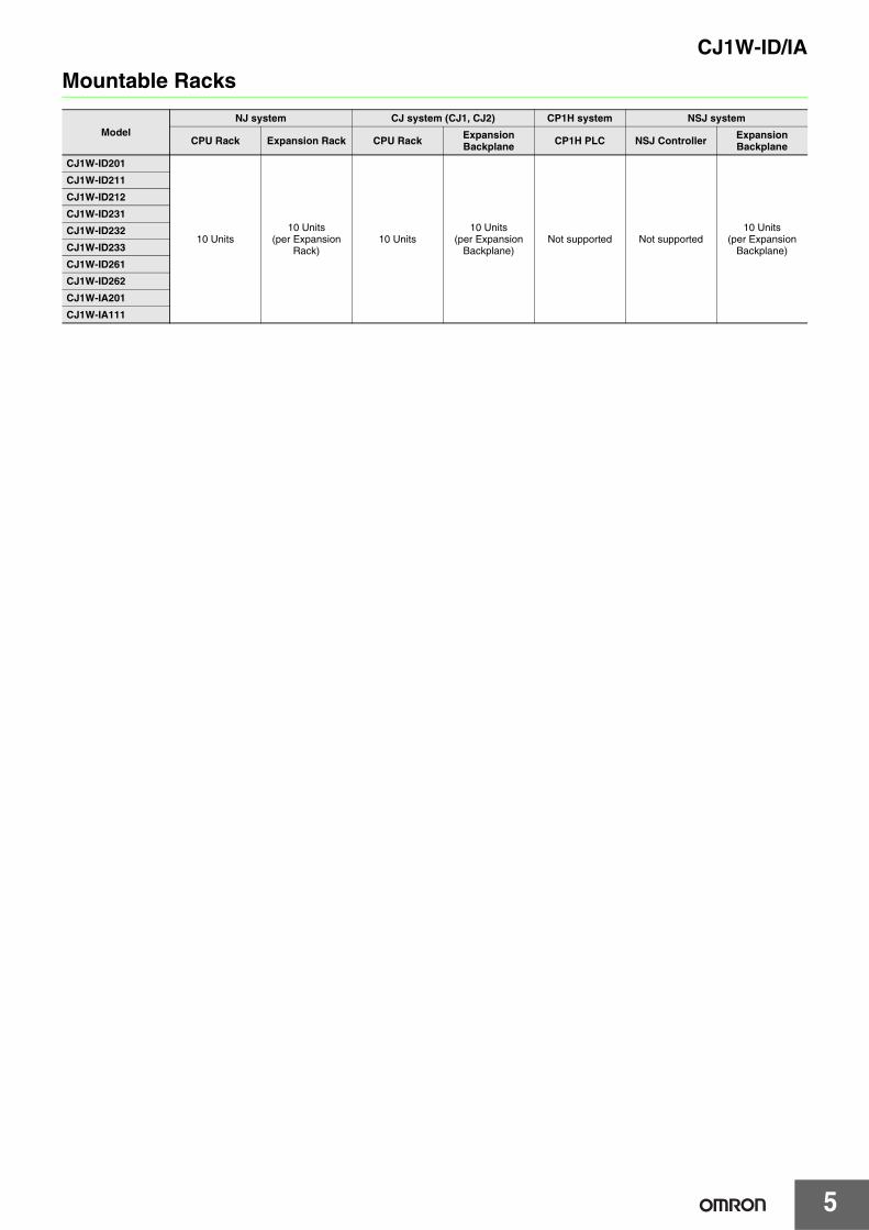
Mountable Racks
ModelNJ system CJ system (CJ1, CJ2) CP1H system NSJ system
CPU Rack Expansion Rack CPU Rack Expansion Backplane CP1H PLC NSJ Controller Expansion
Backplane
CJ1W-ID201
10 Units10 Units
(per Expansion Rack)
10 Units10 Units
(per Expansion Backplane)
Not supported Not supported10 Units
(per Expansion Backplane)
CJ1W-ID211
CJ1W-ID212
CJ1W-ID231
CJ1W-ID232
CJ1W-ID233
CJ1W-ID261
CJ1W-ID262
CJ1W-IA201
CJ1W-IA111

CJ1W-ID/IA
6
SpecificationsCJ1W-ID201 DC Input Unit (12 to 24-VDC, 8 Points)
*1. The ON response time will be 20 μs maximum and OFF response time will be 400 μs maximum even if the response time are set to 0 ms due to internal element delays.
*2. Terminal numbers A0 to A8 and B0 to B8 are used in the external connection and terminal-device variable diagrams. They are not printed on the Units.
Note: Although 16 I/O bits (1 word) are allocated, only 8 of these can be used for external I/O.
Name 8-point DC Input Unit with Terminal Block
Model CJ1W-ID201
Rated Input Voltage 12 to 24 VDC
Rated Input Voltage Range 10.2 to 26.4 VDC
Input Impedance 2.4 kΩ
Input Current 10 mA typical (at 24 VDC)
ON Voltage/ON Current 8.8 VDC min./3 mA min.
OFF Voltage/OFF Current 3 VDC max./1 mA max.
ON Response Time 8.0 ms max. (Can be set to between 0 and 32 ms in the Setup.) *1
OFF Response Time 8.0 ms max. (Can be set to between 0 and 32 ms in the Setup.) *1
Number of Circuits 8 independent circuits
Number of Simultaneously ON Points
100% simultaneously ON
Insulation Resistance 20 MΩ between external terminals and the GR terminal (100 VDC)
Dielectric Strength 1,000 VAC between the external terminals and the GR terminal for 1 minute at a leakage current of 10 mA max.
Internal Current Consumption 80 mA max.
Weight 110 g max.
Circuit Configuration
• The signal names of the terminals are the device variable names. The device variable names are the names that use "Jxx" as the device name.
External connection and terminal-device variable diagram
• Polarity of the input power supply can be connected in either direction.• The signal names of the terminals are the device variable names.
The device variable names are the names that use "Jxx" as the device name.
560
Ω
2.4 kΩ
560
Ω
2.4 kΩ10
00 p
F
Input indicator
Inte
rnal
circ
uits
to
1000
pF
Input indicator
Inte
rnal
circ
uits
Signal name
COM7
Jxx_Ch1_In07
COM0
Jxx_Ch1_In00
Signal name
Signal name
Con-nector pin
12 to 24 VDC
*2
B1
Jxx_Ch1_In00
B2
Jxx_Ch1_In01
B3
Jxx_Ch1_In02
B4
Jxx_Ch1_In03
B5
Jxx_Ch1_In04
B6
Jxx_Ch1_In05
B7
Jxx_Ch1_In06
B8
Jxx_Ch1_In07
NC
C0
C1
C2
C3
C4
C5
C6
C7
NC
B0A1
A2
A3
A4
A5
A6
A7
A8
A0

7
CJ1W-ID/IA
CJ1W-ID211 DC Input Unit (24 VDC, 16 Points)
*1. The ON response time will be 20 μs maximum and OFF response time will be 400 μs maximum even if the response time are set to 0 ms due to internal element delays.
*2. Terminal numbers A0 to A8 and B0 to B8 are used in the external connection and terminal-device variable diagrams. They are not printed on the Units.
Name 16-point DC Input Unit with Terminal Block
Model CJ1W-ID211
Rated Input Voltage 24 VDC
Rated Input Voltage Range 20.4 to 26.4 VDC
Input Impedance 3.3 kΩ
Input Current 7 mA typical (at 24 VDC)
ON Voltage/ON Current 14.4 VDC min./3 mA min.
OFF Voltage/OFF Current 5 VDC max./1 mA max.
ON Response Time 8.0 ms max. (Can be set to between 0 and 32 ms in the Setup.) *1
OFF Response Time 8.0 ms max. (Can be set to between 0 and 32 ms in the Setup.) *1
Number of Circuits 16 (16 points/common, 1 circuit)
Number of Simultaneously ON Points
100% simultaneously ON (at 24 VDC) (Refer to the following illustration.)
Insulation Resistance 20 MΩ between external terminals and the GR terminal (100 VDC)
Dielectric Strength 1,000 VAC between the external terminals and the GR terminal for 1 minute at a leakage current of 10 mA max.
Internal Current Consumption 80 mA max.
Weight 110 g max.
Circuit Configuration
• The signal names of the terminals are the device variable names. The device variable names are the names that use "Jxx" as the device name.
External connection and terminal-device variable diagram
• Polarity of the input power supply can be connected in either direction.• The signal names of the terminals are the device variable names.
The device variable names are the names that use "Jxx" as the device name.
Inte
rnal
circ
uits
Input indicator
to
Signal name
1000 pF
470 Ω3.3 kΩJxx_Ch1_In00
Jxx_Ch1_In15
COM
COM
18
16
14
12
10
8
6
4
2
00 10 20 30 40 50 60
No.
of s
imul
tane
ousl
y O
N p
oint
s
Input voltage: 26.4 VDC12 points at 55°C.
16 points at 45°C.
Ambient temperature(°C)
Temperature characteristics for simultaneously ON points
24 VDC
B1
Jxx_Ch1_In01
B2
Jxx_Ch1_In03
B3
Jxx_Ch1_In05
B4
Jxx_Ch1_In07
B5
Jxx_Ch1_In09
B6
Jxx_Ch1_In11
B7
Jxx_Ch1_In13
B8
Jxx_Ch1_In15
COM
A1
Jxx_Ch1_In00
A2
Jxx_Ch1_In02
A3
Jxx_Ch1_In04
A4
Jxx_Ch1_In06
A5
Jxx_Ch1_In08
A6
Jxx_Ch1_In10
A7
Jxx_Ch1_In12
A8
Jxx_Ch1_In14
COM
B0A0
Signal name
Signal name
Connector pin *2

CJ1W-ID/IA
8
CJ1W-ID212 DC Input Unit (24 VDC, 16 Points)
*1. The ON response time will be 15 μs maximum and OFF response time will be 90 μs maximum even if the response time are set to 0 ms due to internal element delays.
*2. Terminal numbers A0 to A8 and B0 to B8 are used in the external connection and terminal-device variable diagrams. They are not printed on the Units.
Name 16-point DC Input Unit with Terminal Block
Model CJ1W-ID212
Rated Input Voltage 24 VDC
Rated Input Voltage Range 20.4 to 26.4 VDC
Input Impedance 3.3 kΩ
Input Current 7 mA typical (at 24 VDC)
ON Voltage/ON Current 14.4 VDC min./3 mA min.
OFF Voltage/OFF Current 5 VDC max./1 mA max.
ON Response Time 8.0 ms max. (Can be set to between 0 and 32 ms in the Setup.) *1
OFF Response Time 8.0 ms max. (Can be set to between 0 and 32 ms in the Setup.) *1
Number of Circuits 16 (16 points/common, 1 circuit)
Number of Simultaneously ON Points
100% simultaneously ON (at 24 VDC) (Refer to the following illustration.)
Insulation Resistance 20 MΩ between external terminals and the GR terminal (100 VDC)
Dielectric Strength 1,000 VAC between the external terminals and the GR terminal for 1 minute at a leakage current of 10 mA max.
Internal Current Consumption 130 mA max.
Weight 110 g max.
Circuit Configuration
• The signal names of the terminals are the device variable names. The device variable names are the names that use "Jxx" as the device name.
External connection and terminal-device variable diagram
• Polarity of the input power supply can be connected in either direction.• The signal names of the terminals are the device variable names.
The device variable names are the names that use "Jxx" as the device name.
1000 pF
470 Ω3.3 kΩ
Inte
rnal
circ
uits
Input indicator
to
Signal name
Jxx_Ch1_In00
Jxx_Ch1_In15
COM
COM
18
16
14
12
10
8
6
4
2
00 10 20 30 40 50 60
No.
of s
imul
tane
ousl
y O
N p
oint
s
Input voltage: 26.4 VDC12 points at 55°C.
16 points at 45°C.
Ambient temperature(°C)
Temperature characteristics for simultaneously ON points
B1
Jxx_Ch1_In01
B2
Jxx_Ch1_In03
B3
Jxx_Ch1_In05
B4
Jxx_Ch1_In07
B5
Jxx_Ch1_In09
B6
Jxx_Ch1_In11
B7
Jxx_Ch1_In13
B8
Jxx_Ch1_In15
COM
A1
Jxx_Ch1_In00
A2
Jxx_Ch1_In02
A3
Jxx_Ch1_In04
A4
Jxx_Ch1_In06
A5
Jxx_Ch1_In08
A6
Jxx_Ch1_In10
A7
Jxx_Ch1_In12
A8
Jxx_Ch1_In14
COM
B0A0
24 VDC
Signal name
Signal name
Connector pin *2

9
CJ1W-ID/IA
CJ1W-ID231 DC Input Unit (24 VDC, 32 Points)
* The ON response time will be 20 μs maximum and OFF response time will be 400 μs maximum even if the response times are set to 0 ms due to internal element delays.
Note: Observe the following restrictions when connecting to a 2-wire sensor. • Make sure the input power supply voltage is larger than the ON voltage (19 V) plus the residual voltage of the sensor (approx. 3 V). • Use a sensor with a minimum load current of 3 mA min. • Connect bleeder resistance if you connect a sensor with a minimum load current of 5 mA or higher.
Name 32-point DC Input Unit with Fujitsu Connector
Model CJ1W-ID231
Rated Input Voltage 24 VDC
Rated Input Voltage Range 20.4 to 26.4 VDC
Input Impedance 5.6 kΩ
Input Current 4.1 mA typical (at 24 VDC)
ON Voltage/ON Current 19.0 VDC min./3 mA min.
OFF Voltage/OFF Current 5 VDC max./1 mA max.
ON Response Time 8.0 ms max. (Can be set to between 0 and 32 in the Setup.) *
OFF Response Time 8.0 ms max. (Can be set to between 0 and 32 in the Setup.) *
Number of Circuits 32 (16 points/common, 2 circuits)
Number of Simultaneously ON Points 75% (12 points/common) simultaneously ON (at 24 VDC) (Refer to the following illustration.)
Insulation Resistance 20 MΩ between external terminals and the GR terminal (100 VDC)
Dielectric Strength 1,000 VAC between the external terminals and the GR terminal for 1 minute at a leakage current of 10 mA max.
Internal Current Consumption 90 mA max.
Weight 70 g max.
Accessories None
Circuit Configuration
• The signal names of the terminals are the device variable names. The device variable names are the names that use "Jxx" as the device name.
External connection and terminal-device variable diagram
• The input power polarity can be connected in either direction.• Be sure to wire both pins A9 and A18 (COM0), and set the same polarity for both pins.• Be sure to wire both pins B9 and B18 (COM1), and set the same polarity for both pins.• The signal names of the terminals are the device variable names.
The device variable names are the names that use "Jxx" as the device name.
560
Ω56
0 Ω
5.6 kΩ
5.6 kΩ
1000
pF
1000
pF
Inte
rnal
circ
uits
Input indicator
to
toWd m+1
Wd m
Allocated CIO word
Signal name
Connector row A
Connector row B
Jxx_Ch1_In00
Jxx_Ch1_In15
COM0
Jxx_Ch2_In00
Jxx_Ch2_In15
COM1
COM0
COM1
SW
0
5
10
15
20
25
30
35
0 10 20 30 40 50 60
Number of Simultaneously ON Points vs. Ambient Temperature Characteristic
Num
ber
of s
imul
tane
ousl
y O
N p
oint
s
Ambient Temperature
(°C)
10 points/common at 55°C
12 points/common at 55°C
Input voltage: 26.4 VDC
Input voltage: 24 VDC
32 points at 48°C32 points at 40°C
AllocatedCIO word
AllocatedCIO word
Wd m+1Wd m 24 VDC
Wd m Wd m+1
24 VDC
Signal name
Signal name
Connec-tor pin
Jxx_Ch1_In00
Jxx_Ch1_In01
Jxx_Ch1_In02
Jxx_Ch1_In03
Jxx_Ch1_In04
Jxx_Ch1_In05
Jxx_Ch1_In06
Jxx_Ch1_In07
Jxx_Ch2_In00
Jxx_Ch2_In01
Jxx_Ch2_In02
Jxx_Ch2_In03
Jxx_Ch2_In04
Jxx_Ch2_In05
Jxx_Ch2_In06
Jxx_Ch2_In07
COM0
Jxx_Ch1_In08
Jxx_Ch1_In09
Jxx_Ch1_In10
Jxx_Ch1_In11
Jxx_Ch1_In12
Jxx_Ch1_In13
Jxx_Ch1_In14
Jxx_Ch1_In15
Jxx_Ch2_In08
Jxx_Ch2_In09
Jxx_Ch2_In10
Jxx_Ch2_In11
Jxx_Ch2_In12
Jxx_Ch2_In13
Jxx_Ch2_In14
Jxx_Ch2_In15
COM0
NC
NC
COM1
COM1
NC
NC
A1
A2
A3
A4
A5
A6
A7
A8
A9
A10
A11
A12
A13
A14
A15
A16
A17
A18
A19
A20
B1
B2
B3
B4
B5
B6
B7
B8
B9
B10
B11
B12
B13
B14
B15
B16
B17
B18
B19
B20

CJ1W-ID/IA
10
CJ1W-ID232 DC Input Unit (24 VDC, 32 Points)
* The ON response time will be 20 μs maximum and OFF response time will be 400 μs maximum even if the response times are set to 0 ms due to internal element delays.
Note: Observe the following restrictions when connecting to a 2-wire sensor. • Make sure the input power supply voltage is larger than the ON voltage (19 V) plus the residual voltage of the sensor (approx. 3 V). • Use a sensor with a minimum load current of 3 mA min. • Connect bleeder resistance if you connect a sensor with a minimum load current of 5 mA or higher.
Name 32-point DC Input Unit with MIL Connector
Model CJ1W-ID232
Rated Input Voltage 24 VDC
Rated Input Voltage Range 20.4 to 26.4 VDC
Input Impedance 5.6 kΩInput Current 4.1 mA typical (at 24 VDC)
ON Voltage/ON Current 19.0 VDC min./3 mA min.
OFF Voltage/OFF Current 5 VDC max./1 mA max.
ON Response Time 8.0 ms max. (Can be set to between 0 and 32 in the Setup.) *
OFF Response Time 8.0 ms max. (Can be set to between 0 and 32 in the Setup.) *
Number of Circuits 32 (16 points/common, 2 circuits)
Number of Simultaneously ON Points 75% (12 points/common) simultaneously ON (at 24 VDC) (Refer to the following illustration.)
Insulation Resistance 20 MΩ between external terminals and the GR terminal (100 VDC)
Dielectric Strength 1,000 VAC between the external terminals and the GR terminal for 1 minute at a leakage current of 10 mA max.
Internal Current Consumption 90 mA max.
Weight 70 g max.
Accessories None
Circuit Configuration
• The signal names of the terminals are the device variable names. The device variable names are the names that use "Jxx" as the device name.
External connection and terminal-device variable diagram
• The input power polarity can be connected in either direction.• Be sure to wire both pins 23 and 24 (COM0), and set the same polarity for both pins.• Be sure to wire both pins 3 and 4 (COM1), and set the same polarity for both pins.• The signal names of the terminals are the device variable names.
The device variable names are the names that use "Jxx" as the device name.
560
Ω56
0 Ω
5.6 kΩ
5.6 kΩ
1000
pF
1000
pF
Inte
rnal
circ
uits
Input indicator
to
toWd m+1
Wd m
Allocated CIO word
Signal name
Connector row A
Connector row B
Jxx_Ch1_In00
Jxx_Ch1_In15
COM0
Jxx_Ch2_In00
Jxx_Ch2_In15
COM1
COM0
COM1
SW
0
5
10
15
20
25
30
35
0 10 20 30 40 50 60Num
ber
of s
imul
tane
ousl
y O
N p
oint
s
Ambient Temperature(°C)
10 points/common at 55°C
12 points/common at 55°C
Input voltage: 26.4 VDC
Input voltage: 24 VDC
32 points at 48°C32 points at 40°C
Number of Simultaneously ON Points vs. Ambient Temperature Characteristic
Wd m+1 Wd m+1
Wd m Wd m
24 VDC
24 VDC
Signal name
Signal name
Connec-tor pin
Allocated CIO word
Allocated CIO word
2 NC
4 COM1
6 Jxx_Ch2_In07
8 Jxx_Ch2_In06
10 Jxx_Ch2_In05
12 Jxx_Ch2_In04
14 Jxx_Ch2_In03
16 Jxx_Ch2_In02
18 Jxx_Ch2_In01
20 Jxx_Ch2_In00
Jxx_Ch1_In07
Jxx_Ch1_In06
Jxx_Ch1_In05
Jxx_Ch1_In04
Jxx_Ch1_In03
Jxx_Ch1_In02
Jxx_Ch1_In01
Jxx_Ch1_In00
22 NC
24262830323436
1NC
3COM1
5Jxx_Ch2_In15
7Jxx_Ch2_In14
9Jxx_Ch2_In13
11Jxx_Ch2_In12
13Jxx_Ch2_In11
15Jxx_Ch2_In10
17Jxx_Ch2_In09
19Jxx_Ch2_In08
21NC
23252729313335
3840
3739
COM0 COM0
Jxx_Ch1_In15
Jxx_Ch1_In14
Jxx_Ch1_In13
Jxx_Ch1_In12
Jxx_Ch1_In11
Jxx_Ch1_In10
Jxx_Ch1_In09
Jxx_Ch1_In08

11
CJ1W-ID/IA
CJ1W-ID233 DC Input Unit (24 VDC, 32 Points)
* The ON response time will be 15 μs maximum and OFF response time will be 90 μs maximum even if the response times are set to 0 ms due to internal element delays.
Note: Observe the following restrictions when connecting to a 2-wire sensor. • Make sure the input power supply voltage is larger than the ON voltage (19 V) plus the residual voltage of the sensor (approx. 3 V). • Use a sensor with a minimum load current of 3 mA min. • Connect bleeder resistance if you connect a sensor with a minimum load current of 5 mA or higher.
Name 32-point DC Input Unit with MIL Connector
Model CJ1W-ID233
Rated Input Voltage 24 VDC
Rated Input Voltage Range 20.4 to 26.4 VDC
Input Impedance 5.6 kΩInput Current 4.1 mA typical (at 24 VDC)
ON Voltage/ON Current 19.0 VDC min./3 mA min.
OFF Voltage/OFF Current 5 VDC max./1 mA max.
ON Response Time 8.0 ms max. (Can be set to between 0 and 32 in the Setup.) *
OFF Response Time 8.0 ms max. (Can be set to between 0 and 32 in the Setup.) *
Number of Circuits 32 (16 points/common, 2 circuits)
Number of Simultaneously ON Points 75% (12 points/common) simultaneously ON (at 24 VDC) (Refer to the following illustration.)
Insulation Resistance 20 MΩ between external terminals and the GR terminal (100 VDC)
Dielectric Strength 1,000 VAC between the external terminals and the GR terminal for 1 minute at a leakage current of 10 mA max.
Internal Current Consumption 200 mA max.
Weight 70 g max.
Accessories None
Circuit Configuration
• The signal names of the terminals are the device variable names. The device variable names are the names that use "Jxx" as the device name.
External connection and terminal-device variable diagram
• The input power polarity can be connected in either direction.• Be sure to wire both pins 23 and 24 (COM0), and set the same polarity for both pins.• Be sure to wire both pins 3 and 4 (COM1), and set the same polarity for both pins.• The signal names of the terminals are the device variable names.
The device variable names are the names that use "Jxx" as the device name.
560
Ω56
0 Ω
5.6 kΩ
5.6 kΩ
1000
pF
1000
pF
Inte
rnal
circ
uits
Input indicator
to
toWd m+1
Wd m
Allocated CIO word
Signal name
Connector row A
Connector row B
Jxx_Ch1_In00
Jxx_Ch1_In15
COM0
Jxx_Ch2_In00
Jxx_Ch2_In15
COM1
COM0
COM1
SW
0
5
10
15
20
25
30
35
0 10 20 30 40 50 60Num
ber
of s
imul
tane
ousl
y O
N p
oint
s
Ambient Temperature(°C)
10 points/common at 55°C
12 points/common at 55°C
Input voltage: 26.4 VDC
Input voltage: 24 VDC
32 points at 48°C32 points at 40°C
Number of Simultaneously ON Points vs. Ambient Temperature Characteristic
Wd m+1 Wd m+1
Wd m Wd m
24 VDC
24 VDC
Signal name
Signal name
Connec-tor pin
Allocated CIO word
Allocated CIO word
2 NC
4 COM1
6 Jxx_Ch2_In07
8 Jxx_Ch2_In06
10 Jxx_Ch2_In05
12 Jxx_Ch2_In04
14 Jxx_Ch2_In03
16 Jxx_Ch2_In02
18 Jxx_Ch2_In01
20 Jxx_Ch2_In00
Jxx_Ch1_In07
Jxx_Ch1_In06
Jxx_Ch1_In05
Jxx_Ch1_In04
Jxx_Ch1_In03
Jxx_Ch1_In02
Jxx_Ch1_In01
Jxx_Ch1_In00
22 NC
24262830323436
1NC
3COM1
5Jxx_Ch2_In15
7Jxx_Ch2_In14
9Jxx_Ch2_In13
11Jxx_Ch2_In12
13Jxx_Ch2_In11
15Jxx_Ch2_In10
17Jxx_Ch2_In09
19Jxx_Ch2_In08
21NC
23252729313335
3840
3739
COM0 COM0
Jxx_Ch1_In15
Jxx_Ch1_In14
Jxx_Ch1_In13
Jxx_Ch1_In12
Jxx_Ch1_In11
Jxx_Ch1_In10
Jxx_Ch1_In09
Jxx_Ch1_In08

CJ1W-ID/IA
12
CJ1W-ID261 DC Input Unit (24 VDC, 64 Points)
* The ON response time will be 120 μs maximum and OFF response time will be 400 μs maximum even if the response times are set to 0 ms due to internal element delays.
Note: Observe the following restrictions when connecting to a 2-wire sensor. • Make sure the input power supply voltage is larger than the ON voltage (19 V) plus the residual voltage of the sensor (approx. 3 V). • Use a sensor with a minimum load current of 3 mA min. • Connect bleeder resistance if you connect a sensor with a minimum load current of 5 mA or higher.
Name 64-point DC Input Unit with Fujitsu Connector
Model CJ1W-ID261
Rated Input Voltage 24 VDC
Rated Input Voltage Range 20.4 to 26.4 VDC
Input Impedance 5.6 kΩInput Current 4.1 mA typical (at 24 VDC)
ON Voltage/ON Current 19.0 VDC min./3 mA min.
OFF Voltage/OFF Current 5 VDC max./1 mA max.
ON Response Time 8.0 ms max. (Can be set to between 0 and 32 in the Setup.) *
OFF Response Time 8.0 ms max. (Can be set to between 0 and 32 in the Setup.) *
Number of Circuits 64 (16 points/common, 4 circuits)
Number of Simultaneously ON Points 50% (16 points/common) simultaneously ON (at 24 VDC) (Refer to the following illustrations.)
Insulation Resistance 20 MΩ between external terminals and the GR terminal (100 VDC)
Dielectric Strength 1,000 VAC between the external terminals and the GR terminal for 1 minute at a leakage current of 10 mA max.
Internal Current Consumption 90 mA max.
Weight 110 g max.
Accessories None
Circuit Configuration
• The signal names of the terminals are the device variable names. The device variable names are the names that use "Jxx" as the device name.
External connection and terminal-device variable diagram
CN1 CN2
• The input power polarity can be connected in either direction.• Be sure to wire both pins A9 and A18 (COM0) of CN1, and set the
same polarity for both pins.• Be sure to wire both pins B9 and B18 (COM1) of CN1, and set the
same polarity for both pins.• The signal names of the terminals are the device variable names.
The device variable names are the names that use "Jxx" as the device name.
• The input power polarity can be connected in either direction.• Be sure to wire both pins A9 and A18 (COM2) of CN2, and set the
same polarity for both pins.• Be sure to wire both pins B9 and B18 (COM3) of CN2, and set the
same polarity for both pins.• The signal names of the terminals are the device variable names.
The device variable names are the names that use "Jxx" as the device name.
5.6 kΩ
1000
pF
560
Ω
5.6 kΩ
Input indicatorIndicator switching circuit
Inte
rnal
circ
uits
Inte
rnal
circ
uits
1000
pF
560
Ω
Wd m+1
Wd m
Wd m+2
Wd m+3
Allocated CIO word
Signal name
Connector row A
Connector row B
Connector row A
Connector row B
SWCN1
Jxx_Ch1_In00
Jxx_Ch1_In15COM0
Jxx_Ch2_In00
Jxx_Ch2_In15
COM0
COM1COM1
Jxx_Ch3_In00
Jxx_Ch3_In15COM2
Jxx_Ch4_In00
Jxx_Ch4_In15
COM2
COM3COM3
CN2
to
to
to
to
0
10
20
30
40
50
60
70
0 10 20 30 40 50 60
Ambient Temperature
8 points/common (total: 26 points max.) at 55°C
8 points/common at 55°C
12 points/common (total: 45 points) at 55°C
Input voltage: 20.4 VDC
Input voltage: 26.4 VDC
Input voltage: 24 VDC
Num
ber
of s
imul
tane
ousl
y O
N p
oint
s
Number of Simultaneously ON Points vs. Ambient Temperature Characteristic
64 points at 25°C 64 points at 47°C
(°C)
64 points at 35°C
24 VDC
Wd
m+
1
Wd
m
Wd
m
24 VDC
Wd
m+
1
Signal name
Signal name
Connec-tor pin
Allocated CIO word
Allocated CIO word
COM0
COM0
NC
NC
COM1
COM1
NC
NC
Jxx_Ch1_In07
Jxx_Ch1_In06
Jxx_Ch1_In05
Jxx_Ch1_In04
Jxx_Ch1_In03
Jxx_Ch1_In02
Jxx_Ch1_In01
Jxx_Ch1_In00
Jxx_Ch2_In07
Jxx_Ch2_In06
Jxx_Ch2_In05
Jxx_Ch2_In04
Jxx_Ch2_In03
Jxx_Ch2_In02
Jxx_Ch2_In01
Jxx_Ch2_In00
Jxx_Ch1_In15
Jxx_Ch1_In14
Jxx_Ch1_In13
Jxx_Ch1_In12
Jxx_Ch1_In11
Jxx_Ch1_In10
Jxx_Ch1_In09
Jxx_Ch1_In08
Jxx_Ch2_In15
Jxx_Ch2_In14
Jxx_Ch2_In13
Jxx_Ch2_In12
Jxx_Ch2_In11
Jxx_Ch2_In10
Jxx_Ch2_In09
Jxx_Ch2_In08
A20
A19
A18
A17
A16
A15
A14
A13
A12
A11
A10
A9
A8
A7
A6
A5
A4
A3
A2
A1
B20
B19
B18
B17
B16
B15
B14
B13
B12
B11
B10
B9
B8
B7
B6
B5
B4
B3
B2
B1
Wd
m+
2
24VDC
Wd
m+
2
24 VDC
Wd
m+
3W
d m
+3
Signal name
Signal name
Connec-tor pin
Allocated CIO word
Allocated CIO word
COM3
COM3
NC
NC
COM2
COM2
NC
NC
Jxx_Ch3 _In08
Jxx_Ch3_In09
Jxx_Ch3_In10
Jxx_Ch3_In11
Jxx_Ch3_In12
Jxx_Ch3_In13
Jxx_Ch3_In14
Jxx_Ch3_In15
Jxx_Ch4_In08
Jxx_Ch4_In09
Jxx_Ch4_In10
Jxx_Ch4_In11
Jxx_Ch4_In12
Jxx_Ch4_In13
Jxx_Ch4_In14
Jxx_Ch4_In15
Jxx_Ch3_In00
Jxx_Ch3_In01
Jxx_Ch3_In02
Jxx_Ch3_In03
Jxx_Ch3_In04
Jxx_Ch3_In05
Jxx_Ch3_In06
Jxx_Ch3_In07
Jxx_Ch4_In00
Jxx_Ch4_In01
Jxx_Ch4_In02
Jxx_Ch4_In03
Jxx_Ch4_In04
Jxx_Ch4_In05
Jxx_Ch4_In06
Jxx_Ch4_In07
B1
B2
B3
B4
B5
B6
B7
B8
B9
B10
B11
B12
B13
B14
B15
B16
B17
B18
B19
B20
A1
A2
A3
A4
A5
A6
A7
A8
A9
A10
A11
A12
A13
A14
A15
A16
A17
A18
A19
A20

13
CJ1W-ID/IA
CJ1W-ID262 DC Input Unit (24 VDC, 64 Points)
* The ON response time will be 120 μs maximum and OFF response time will be 400 μs maximum even if the response times are set to 0 ms due to internal element delays.
Note: Observe the following restrictions when connecting to a 2-wire sensor. • Make sure the input power supply voltage is larger than the ON voltage (19 V) plus the residual voltage of the sensor (approx. 3 V). • Use a sensor with a minimum load current of 3 mA min. • Connect bleeder resistance if you connect a sensor with a minimum load current of 5 mA or higher.
Name 64-point DC Input Unit with MIL ConnectorModel CJ1W-ID262Rated Input Voltage 24 VDCRated Input Voltage Range 20.4 to 26.4 VDC
Input Impedance 5.6 kΩInput Current 4.1 mA typical (at 24 VDC)ON Voltage/ON Current 19.0 VDC min./3 mA min.OFF Voltage/OFF Current 5 VDC max./1 mA max.ON Response Time 8.0 ms max. (Can be set to between 0 and 32 in the Setup.) *OFF Response Time 8.0 ms max. (Can be set to between 0 and 32 in the Setup.) *Number of Circuits 64 (16 points/common, 4 circuits)Number of Simultaneously ON Points 50% (8 points/common) simultaneously ON (at 24 VDC) (Refer to the following illustrations.)
Insulation Resistance 20 MΩ between external terminals and the GR terminal (100 VDC)Dielectric Strength 1,000 VAC between the external terminals and the GR terminal for 1 minute at a leakage current of 10 mA max.Internal Current Consumption 90 mA max.
Weight 110 g max.Accessories None
Circuit Configuration
• The signal names of the terminals are the device variable names. The device variable names are the names that use "Jxx" as the device name.
External connection and terminal-device variable diagram
CN1 CN2
• The input power polarity can be connected in either direction.• Be sure to wire both pins 23 and 24 (COM0) of CN1, and set the
same polarity for both pins.• Be sure to wire both pins 3 and 4 (COM1) of CN1, and set the
same polarity for both pins.• The signal names of the terminals are the device variable names.
The device variable names are the names that use "Jxx" as the device name.
• The input power polarity can be connected in either direction.• Be sure to wire both pins 23 and 24 (COM2) of CN2, and set the
same polarity for both pins.• Be sure to wire both pins 3 and 4 (COM3) of CN2, and set the
same polarity for both pins.• The signal names of the terminals are the device variable names.
The device variable names are the names that use "Jxx" as the device name.
to
to
to
to
Input indicatorIndicator switching circuit
Inte
rnal
circ
uits
Inte
rnal
circ
uits
Wd m+1
Wd m
Wd m+2
Wd m+3
Allocated CIO word
Signal name
Jxx_Ch1_In00
Jxx_Ch1_In15COM0
SWJxx_Ch2_In00
Jxx_Ch2_In15
CN1COM0
COM1 COM1
Jxx_Ch3_In00
Jxx_Ch3_In15COM2
Jxx_Ch4_In00
Jxx_Ch4_In15
COM2
COM3COM3
560
Ω56
0 Ω
1000
pF10
00pF
5.6 kΩ
5.6 kΩ
CN20
10
20
30
40
50
60
70
0 10 20 30 40 50 60
Ambient Temperature
8 points/common (total: 26 points max.) at 55°C
8 points/common at 55°C
12 points/common (total: 45 points) at 55°C
Input voltage: 20.4 VDC
Input voltage: 26.4 VDC
Input voltage: 24 VDC
Num
ber
of s
imul
tane
ousl
y O
N p
oint
s
Number of Simultaneously ON Points vs. Ambient Temperature Characteristic
64 points at 47°C64 points at 35°C64 points at 25°C
(°C)
24 VDC
24 VDC
Wd
m+
1
Wd
m+
1
Wd
m
Wd
m
Signal name
Signal name
Connec-tor pin
Allocated CIO word
Allocated CIO word
1NC
35791113151719212325272931333537
NC
39
24
NC
681012141618
COM1
2022242628303234363840
COM1
NC
COM0 COM0
Jxx_Ch1_In00
Jxx_Ch1_In01
Jxx_Ch1_In02
Jxx_Ch1_In03
Jxx_Ch1_In04
Jxx_Ch1_In05
Jxx_Ch1_In06
Jxx_Ch1_In07
Jxx_Ch2_In00
Jxx_Ch2_In01
Jxx_Ch2_In02
Jxx_Ch2_In03
Jxx_Ch2_In04
Jxx_Ch2_In05
Jxx_Ch2_In06
Jxx_Ch2_In07
Jxx_Ch2_In08
Jxx_Ch2_In09
Jxx_Ch2_In10
Jxx_Ch2_In11
Jxx_Ch2_In12
Jxx_Ch2_In13
Jxx_Ch2_In14
Jxx_Ch2_In15
Jxx_Ch1_In08
Jxx_Ch1_In09
Jxx_Ch1_In10
Jxx_Ch1_In11
Jxx_Ch1_In12
Jxx_Ch1_In13
Jxx_Ch1_In14
Jxx_Ch1_In15
Wd
m+
3
Wd
m+
3
Wd
m+
2
Wd
m+
2
24 VDC
24 VDC
Signal name
Signal name
Connec-tor pin
Allocated CIO word
Allocated CIO word
40383634323028262422201816141210864
NC2COM3
393735333129272523
COM22119171513119753
NC 1COM3
COM2
NC
Jxx_Ch3_In15
Jxx_Ch3_In14
Jxx_Ch3_In13
Jxx_Ch3_In12
Jxx_Ch3_In11
Jxx_Ch3_In10
Jxx_Ch3_In09
Jxx_Ch3_In08
Jxx_Ch4_In15
Jxx_Ch4_In14
Jxx_Ch4_In13
Jxx_Ch4_In12
Jxx_Ch4_In11
Jxx_Ch4_In10
Jxx_Ch4_In09
Jxx_Ch4_In08
Jxx_Ch4_In07
Jxx_Ch4_In06
Jxx_Ch4_In05
Jxx_Ch4_In04
Jxx_Ch4_In03
Jxx_Ch4_In02
Jxx_Ch4_In01
Jxx_Ch4_In00
Jxx_Ch3_In07
Jxx_Ch3_In06
Jxx_Ch3_In05
Jxx_Ch3_In04
Jxx_Ch3_In03
Jxx_Ch3_In02
Jxx_Ch3_In01
Jxx_Ch3_In00
NC

CJ1W-ID/IA
14
CJ1W-IA201 AC Input Unit (200 VAC, 8 Points)
*1. Can be set to 0 ms, 0.5 ms, 1 ms, 2 ms, 4 ms, 8 ms, 16 ms, or 32ms in the settings. When the response times have been set to 0 ms, the ON response time will be 10 ms maximum and the OFF response time will be 40 ms maximum due to internal element delays.
*2. Terminal numbers A0 to A8 and B0 to B8 are used in the external connection and terminal-device variable diagrams. They are not printed on the Units.
Note: Although 16 I/O bits (1 word) are allocated, only 8 of these can be used for external I/O.
Name 8-point AC Input Unit with Terminal Block
Model CJ1W-IA201
Rated Input Voltage 200 to 240 VAC 50/60 Hz
Rated Input Voltage Range 170 to 264 VAC
Input Impedance 21 kΩ (50 Hz), 18 kΩ (60 Hz)
Input Current 9 mA typical (at 200 VAC, 50 Hz), 11 mA typical (at 200 VAC, 60 Hz)
ON Voltage/ON Current 120 VAC min./4 mA min.
OFF Voltage/OFF Current 40 VAC max./2 mA max.
ON Response Time 18.0 ms max. (default setting: 8 ms) *1
OFF Response Time 48.0 ms max. (default setting: 8 ms) *1
Number of Circuits 8 (8 points/common, 1 circuit)
Number of Simultaneously ON Points
100% (8 points/common) simultaneously ON
Insulation Resistance 20 MΩ between external terminals and the GR terminal (500 VDC)
Dielectric Strength 2,000 VAC between the external terminals and the GR terminal for 1 minute at a leakage current of 10 mA max.
Internal Current Consumption 80 mA max.
Weight 130 g max.
Accessories None
Circuit Configuration
• The signal names of the terminals are the device variable names. The device variable names are the names that use "Jxx" as the device name.
External connection and terminal-device variable diagram
• The signal names of the terminals are the device variable names. The device variable names are the names that use "Jxx" as the device name.
820 Ω 1 MΩ
0.15 μF 220 Ω
Input indicator
Inte
rnal
circ
uits
to
Signal name
COM
Jxx_Ch1_In00
Jxx_Ch1_In07
200 to 240 VAC
Signal name
Connec-tor pin *2
Jxx_Ch1_In00
Jxx_Ch1_In01
Jxx_Ch1_In02
Jxx_Ch1_In03
Jxx_Ch1_In05
Jxx_Ch1_In06
Jxx_Ch1_In07
B0
B1
B2
B3
B4
B5
B6
B7
B8
Jxx_Ch1_In04
A0
A1
A2
A3
A4
A5
A6
A7
A8 COM
NC
NC
NC
NC
NC
NC
NC
NC
NC

15
CJ1W-ID/IA
CJ1W-IA111 AC Input Unit (100 VAC, 16 points)
*1. Can be set to 0 ms, 0.5 ms, 1 ms, 2 ms, 4 ms, 8 ms, 16 ms, or 32ms in the settings. When the response times have been set to 0 ms, the ON response time will be 10 ms maximum and the OFF response time will be 40 ms maximum due to internal element delays.
*2. Use an input voltage of 90 VAC or higher when connecting 2-wire sensors.*3. Terminal numbers A0 to A8 and B0 to B8 are used in the external connection and terminal-device variable diagrams. They are not printed on
the Units.
Name 16-point AC Input Unit with Terminal Block
Model CJ1W-IA111
Rated input voltage 100 to 120 VAC 50/60 Hz *2
Rated Input Voltage Range 85 to 132 VAC
Input Impedance 14.5 kΩ (50 Hz), 12 kΩ (60 Hz)
Input Current 7 mA typical (at 100 VAC, 50 Hz), 8 mA typical (at 100 VAC, 60 Hz)
ON Voltage/ON Current 70 VAC min./4 mA min
OFF Voltage/OFF Current 20 VAC max./2 mA max
ON Response Time 18 ms max. (default setting: 8 ms) *1
OFF Response Time 48 ms max. (default setting: 8 ms) *1
Number of Circuits 16 (16 points/common, 1 circuit)
Number of Inputs ON Simultaneously 100% simultaneously ON (16 points/common)
Insulation Resistance 20 MΩ between external terminals and the GR terminal (500 VDC)
Dielectric Strength 2,000 VAC between the external terminals and the GR terminal for 1 minute at a leakage current of 10 mA max.
Internal Current Consumption 90 mA max.
Weight 130 g max.
Accessories None
Circuit Layout
• The signal names of the terminals are the device variable names. The device variable names are the names that use "Jxx" as the device name.
External connection and terminal-device variable diagram
• The signal names of the terminals are the device variable names. The device variable names are the names that use "Jxx" as the device name.
470 Ω 1 MΩ
0.22 μF 270 Ω
Input indicator
Inte
rnal
circ
uits
to
Signal name
COM
Jxx_Ch1_In00
Jxx_Ch1_In15
100 to 120 VAC
Signal name
Signal name
Connec-tor pin*3
A0
A1
A2
A3
A4
A5
A6
A7
A8
B0
B1
B2
B3
B4
B5
B6
B7
B8
COMCOM
Jxx_Ch1_In00
Jxx_Ch1_In02
Jxx_Ch1_In04
Jxx_Ch1_In06
Jxx_Ch1_In08
Jxx_Ch1_In10
Jxx_Ch1_In12
Jxx_Ch1_In14
Jxx_Ch1_In01
Jxx_Ch1_In03
Jxx_Ch1_In05
Jxx_Ch1_In07
Jxx_Ch1_In09
Jxx_Ch1_In11
Jxx_Ch1_In13
Jxx_Ch1_In15

16
CJ1W-ID/IA
Bit Allocations for Input Unit8-point Input Unit 16-point Input Unit
32-point Input Unit 64-point Input Unit
Allocated CIO wordSignal name (CJ/NJ)
CIO Bit
Wd m(Input)
00 IN0/Jxx_Ch1_In00
01 IN1/Jxx_Ch1_In01
: :
06 IN6/Jxx_Ch1_In06
07 IN7/Jxx_Ch1_In07
08 −
09 −
: :
14 −
15 −
Allocated CIO wordSignal name (CJ/NJ)
CIO Bit
Wd m(Input)
00 IN0/Jxx_Ch1_In00
01 IN1/Jxx_Ch1_In01
: :
14 IN14/Jxx_Ch1_In14
15 IN15/Jxx_Ch1_In15
Allocated CIO wordSignal name (CJ/NJ)
CIO Bit
Wd m(Input)
00 IN0/Jxx_Ch1_In00
01 IN1/Jxx_Ch1_In01
: :
14 IN14/Jxx_Ch1_In14
15 IN15/Jxx_Ch1_In15
Wd m+1(Input)
00 IN0/Jxx_Ch2_In00
01 IN1/Jxx_Ch2_In01
: :
14 IN14/Jxx_Ch2_In14
15 IN15/Jxx_Ch2_In15
Allocated CIO wordSignal name (CJ/NJ)
CIO Bit
Wd m(Input)
00 IN0/Jxx_Ch1_In00
01 IN1/Jxx_Ch1_In01
: :
14 IN14/Jxx_Ch1_In14
15 IN15/Jxx_Ch1_In15
Wd m+1(Input)
00 IN0/Jxx_Ch2_In00
01 IN1/Jxx_Ch2_In01
: :
14 IN14/Jxx_Ch2_In14
15 IN15/Jxx_Ch2_In15
Wd m+2(Input)
00 IN0/Jxx_Ch3_In00
01 IN1/Jxx_Ch3_In01
: :
14 IN14/Jxx_Ch3_In14
15 IN15/Jxx_Ch3_In15
Wd m+3(Input)
00 IN0/Jxx_Ch4_In00
01 IN1/Jxx_Ch4_In01
: :
14 IN14/Jxx_Ch4_In14
15 IN15/Jxx_Ch4_In15

17
CJ1W-ID/IA
External Interface8-point/16-point Units (18-point Terminal Blocks)
32-point Units (Models with 40-point Fujitsu Connector or MIL Connector)
ERR0 1 2 3 4 5 6 7
8 9 10 11 12 13 14 15
ConnectorConnect to the connector on the next Unit.
I/O indicators
Model number label
Terminal block for I/O wiring, 18P × 1
ID231 ID232 1 2
0 1 2 34 5 6 78 912 13 14 15
10 11
ERR
Model number
I/O indicators
Unit with MIL ConnectorUnit with Fujitsu-compatibleConnector
ConnectorConnected to the connector on the next Unit.
Indicator Switch
Changes the 16 I/O displayed on the I/O indicators.
Word morm+1
I/O wiringconnector(40-pin × 1) Wd m (Row A on connector)
Fujitsu connector MIL connectorBottom of connectorTop of connectorWd m+1 (Row B on connector)
Setting 1Setting 2

CJ1W-ID/IA
18
64-point Units (Models with Two 40-point Fujitsu Connectors or MIL Connector)
Wiring Basic I/O Units with Terminal BlocksElectric WiresThe following wire gauges are recommended.
Crimp terminalsUse crimp terminals (M3) having the dimensions shown below.
Terminal Block Connector Wire Size
18-terminal AWG 22 to 18 (0.32 to 0.82 mm2)
ID261
0 1 2 3 4 5 6 78 9 12 13 14 1510 110 1 2 3 4 5 6 78 9 12 13 14 1510 11
I
II
ID261
1 2Model number
I/O indicators
Unit with MIL ConnectorUnit with Fujitsu-compatibleConnector
ConnectorConnected to the connector on the next Unit.
Indicator Switch
Changes the 32 I/O displayed on the I/O indicators.
Setting 1Setting 2
I/O wiringconnector(40-pin × 2)
Wd m and m+1: CN1Wd m+2 and m+3: CN2
Word m orm+2Word m+1or m+3
6.2 mm max. 6.2 mm max.

19
CJ1W-ID/IA
I/O Unit Wiring MethodsAn I/O Unit can be connected to an external device by any of the following three methods.
1. User-provided CableAn I/O Unit can be directly connected to an external device by using a connector.
2. Connector-Terminal Block Conversion UnitUse a Connecting Cable to connect to a Connector-Terminal Block Conversion Unit. Converting the I/O Unit connector to a screw terminal block makes it easy to connect external devices.
3. I/O Relay TerminalUse a Connecting Cable to connect to an I/O Relay Terminal. The I/O specifications can be converted to relay outputs and AC inputs by connecting the I/O Relay Terminal to an I/O Unit.
B
C
A
A User-provided cable
B External device
C Connector
B
C
A
A Connecting Cable for Connector-Terminal Block Conversion UnitXW2Z
B Connector-Terminal Block Conversion UnitXW2@
C Conversion to a screw terminal block
B
B
A
A G79 I/O Relay Terminal Connecting Cable
B G7@@ I/O Relay TerminalsOr, conversion to relay outputs and AC inputs.

CJ1W-ID/IA
20
1. Using User-made Cables with ConnectorAvailable ConnectorsUse the following connectors when assembling a connector and cable.
32- and 64-point Basic I/O Units with Fujitsu-compatible ConnectorsApplicable Units
Applicable Cable-side Connectors
32- and 64-point Basic I/O Units with MIL ConnectorsApplicable Units
Applicable Cable-side Connectors
Wire SizeWe recommend using cable with wire gauges of AWG 24 or AWG 28 (0.2 mm2 to 0.08 mm2). Use cable with external wire diameters of 1.61 mm max.
Crimping ToolsThe following models are recommended for crimping tools and pressure-welding tools for Fujitsu connectors. Tools for Crimped Connectors (Fujitsu Component)
Tools for Pressure-welded Connectors (Fujitsu Component)
The following models are recommended for crimping tools for MIL connectors.Tools for Crimped Connectors (OMRON)
Model Specifications Pins
CJ1W-ID231 Input Unit, 24 VDC, 32 inputs 40
CJ1W-ID261 Input Unit, 24 VDC, 64 inputs
Connection Pins OMRON set Fujitsu parts
Solder-type 40 C500-CE404 Socket: FCN-361J040-AUConnector cover: FCN-360C040-J2
Crimped 40 C500-CE405Socket: FCN-363J040Connector cover: FCN-360C040-J2Contacts: FCN-363J-AU
Pressure-welded 40 C500-CE403 FCN-367J040-AU/F
Model Specifications Pins
CJ1W-ID232CJ1W-ID233 Input Unit, 24 VDC, 32 inputs
40CJ1W-ID262 Input Unit, 24 VDC, 64 inputs
Connection Pins OMRON set DDK parts
Pressure-welded 40 XG4M-4030-T FRC5-A040-3T0S
Product Name Model
Hand Crimping Tool FCN-363T-T005/H
Contact Withdrawal Tool FCN-360T-T001/H
Product Name Model
Hand Press FCN-707T-T101/H
Cable Cutter FCN-707T-T001/H
Locator Plate FCN-367T-T012/H
Product Name Model
Crimping Tool XY2B-0002
Attachment XY2B-1007

21
CJ1W-ID/IA
2. Connecting Connector-Terminal Block Conversion UnitsConnection Patterns for Connector-Terminal Block Conversion Units
Combination of I/O Units with Connector-Terminal Block Conversion Units
Pattern Configuration Number of connectors Branching
A
1
None
B 2 branches
D
2
None
F 2 branches
Unit I/O capacity Number of connectors Polarity Connection
patternNumber of branches
Connecting Cable
Connector-Terminal Block Conversion Unit
Common terminal
CJ1W-ID231 32 inputs 1 Fujitsu connector NPN/PNP
A None XW2Z-@@@B XW2D-40G6 None
A None XW2Z-@@@B XW2D-40G6-RF *2 None
A None XW2Z-@@@B XW2B-40G5 None
A None XW2Z-@@@B XW2B-40G4 None
A None XW2Z-@@@BU XW2D-40C6 None
B 2 XW2Z-@@@D XW2D-20G6 (2 Units) None
B 2 XW2Z-@@@D XW2B-20G5 (2 Units) None
B 2 XW2Z-@@@D XW2B-20G4 (2 Units) None
B 2 XW2Z-@@@D XW2C-20G6-IO16 (2 Units) Yes
B 2 XW2Z-@@@D XW2C-20G5-IN16 (2 Units) *1 Yes
B 2 XW2Z-@@@D XW2E-20G5-IN16 (2 Units) *1 Yes
B 2 XW2Z-@@@D XW2F-20G7-IN16 (2 Units) *1 Yes
B 2 XW2Z-@@@D XW2N-20G8-IN16 (2 Units) *1 Yes
Connecting Cable
Connector-Terminal Block Conversion Unit
40 or 60 terminals
Connecting Cable with two branches
Connector-Terminal Block Conversion Unit
20 terminals 20 terminals
Connecting Cable
Connector-Terminal Block Conversion Unit
40 or 60 terminals 40 or 60 terminals
Connecting Cable with two branches
Connector-Terminal Block Conversion Unit
20 terminals 20 terminals 20 terminals 20 terminals

22
CJ1W-ID/IA
*1. The inputs are NPN. For PNP inputs, reverse the polarity of the external power supply connections to the power supply terminals on the Connector-Terminal Block Conversion Unit.
*2. Bleeder resistance (5.6 kΩ) is built in.
CJ1W-ID232 32 inputs 1 MIL connector NPN/PNP
A None XW2Z-@@@K XW2D-40G6 None
A None XW2Z-@@@K XW2D-40G6-RM *2 None
A None XW2Z-@@@K XW2B-40G5 None
A None XW2Z-@@@K XW2B-40G4 None
B 2 XW2Z-@@@N XW2D-20G6 (2 Units) None
B 2 XW2Z-@@@N XW2B-20G5 (2 Units) None
B 2 XW2Z-@@@N XW2B-20G4 (2 Units) None
B 2 XW2Z-@@@N XW2C-20G6-IO16 (2 Units) Yes
B 2 XW2Z-@@@N XW2C-20G5-IN16 (2 Units) *1 Yes
B 2 XW2Z-@@@N XW2E-20G5-IN16 (2 Units) *1 Yes
B 2 XW2Z-@@@N XW2F-20G7-IN16 (2 Units) *1 Yes
B 2 XW2Z-@@@N XW2N-20G8-IN16 (2 Units) *1 Yes
CJ1W-ID233 32 inputs 1 MIL connector NPN/PNP
A None XW2Z-@@@K XW2D-40G6 None
A None XW2Z-@@@K XW2D-40G6-RM *2 None
A None XW2Z-@@@K XW2B-40G5 None
A None XW2Z-@@@K XW2B-40G4 None
B 2 XW2Z-@@@N XW2D-20G6 (2 Units) None
B 2 XW2Z-@@@N XW2B-20G5 (2 Units) None
B 2 XW2Z-@@@N XW2B-20G4 (2 Units) None
B 2 XW2Z-@@@N XW2C-20G6-IO16 (2 Units) Yes
B 2 XW2Z-@@@N XW2C-20G5-IN16 (2 Units) *1 Yes
B 2 XW2Z-@@@N XW2E-20G5-IN16 (2 Units) *1 Yes
B 2 XW2Z-@@@N XW2F-20G7-IN16 (2 Units) *1 Yes
B 2 XW2Z-@@@N XW2N-20G8-IN16 (2 Units) *1 Yes
CJ1W-ID261 64 inputs 2 Fujitsu connectors NPN/PNP
D None XW2Z-@@@B XW2D-40G6 None
D None XW2Z-@@@B XW2D-40G6-RF *2 None
D None XW2Z-@@@B XW2B-40G5 None
D None XW2Z-@@@B XW2B-40G4 None
D None XW2Z-@@@BU XW2D-40C6 None
F 2 XW2Z-@@@D XW2D-20G6 (2 Units) None
F 2 XW2Z-@@@D XW2B-20G5 (2 Units) None
F 2 XW2Z-@@@D XW2B-20G4 (2 Units) None
F 2 XW2Z-@@@D XW2C-20G6-IO16 (2 Units) Yes
F 2 XW2Z-@@@D XW2C-20G5-IN16 (2 Units) *1 Yes
F 2 XW2Z-@@@D XW2E-20G5-IN16 (2 Units) *1 Yes
F 2 XW2Z-@@@D XW2F-20G7-IN16 (2 Units) *1 Yes
F 2 XW2Z-@@@D XW2N-20G8-IN16 (2 Units) *1 Yes
CJ1W-ID262 64 inputs 2 MIL connectors NPN/PNP
D None XW2Z-@@@K XW2D-40G6 None
D None XW2Z-@@@K XW2D-40G6-RM *2 None
D None XW2Z-@@@K XW2B-40G5 None
D None XW2Z-@@@K XW2B-40G4 None
F 2 XW2Z-@@@N XW2D-20G6 (2 Units) None
F 2 XW2Z-@@@N XW2B-20G5 (2 Units) None
F 2 XW2Z-@@@N XW2B-20G4 (2 Units) None
F 2 XW2Z-@@@N XW2C-20G6-IO16 (2 Units) Yes
F 2 XW2Z-@@@N XW2C-20G5-IN16 (2 Units) *1 Yes
F 2 XW2Z-@@@N XW2E-20G5-IN16 (2 Units) *1 Yes
F 2 XW2Z-@@@N XW2F-20G7-IN16 (2 Units) *1 Yes
F 2 XW2Z-@@@N XW2N-20G8-IN16 (2 Units) *1 Yes
Unit I/O capacity Number of connectors Polarity Connection
patternNumber of branches
Connecting Cable
Connector-Terminal Block Conversion Unit
Common terminal

23
CJ1W-ID/IA
Types of Connecting Cables
Cable lenght XW2Z-@@A XW2Z-@@B XW2Z-@@BU XW2Z-@@D XW2Z-@@L XW2Z-@@X
0.25m − − − − − −
0.5m XW2Z-050A XW2Z-050B XW2Z-050BU − − XW2Z-C50X
1.0m XW2Z-100A XW2Z-100B XW2Z-100BU XW2Z-100D XW2Z-100L XW2Z-100X
1.5m XW2Z-150A XW2Z-150B XW2Z-150BU XW2Z-150D XW2Z-150L −
2.0m XW2Z-200A XW2Z-200B XW2Z-200BU XW2Z-200D XW2Z-200L XW2Z-200X
3.0m XW2Z-300A XW2Z-300B XW2Z-300BU XW2Z-300D XW2Z-300L XW2Z-300X
5.0m XW2Z-500A XW2Z-500B XW2Z-500BU XW2Z-500D XW2Z-500L XW2Z-500X
10.0m XW2Z-010A XW2Z-010B − XW2Z-010D XW2Z-010L XW2Z-010X
15.0m XW2Z-15MA XW2Z-15MB − XW2Z-15MD XW2Z-15ML −
20.0m XW2Z-20MA XW2Z-20MB − XW2Z-20MD XW2Z-20ML −

CJ1W-ID/IA
24
3. Connecting I/O Relay TerminalsConnection Patterns for I/O Relay Terminals
Combination of I/O Units with I/O Relay Terminal and Connecting Cables
Types of Connecting Cables
Pattern Configuration
A
B
Model I/O points Number of connectors Polarity Connection
patternNumber of branches Connecting Cable I/O Relay Terminal
CJ1W-ID231 32 inputs 1 Fujitsu connector NPN
A 2 G79-I@C-@ G7TC-ID16
A 2 G79-I@C-@ G7TC-IA16
CJ1W-ID232 32 inputs 1 MIL connector NPNA 2 G79-O@-@-D1 G7TC-ID16
A 2 G79-O@-@-D1 G7TC-IA16
CJ1W-ID233 32 inputs 1 MIL connector NPNA 2 G79-O@-@-D1 G7TC-ID16
A 2 G79-O@-@-D1 G7TC-IA16
CJ1W-ID261 64 inputs 2 Fujitsu connectors NPN
B 2 G79-I@C-@ G7TC-ID16
B 2 G79-I@C-@ G7TC-IA16
CJ1W-ID262 64 inputs 2 MIL connectors NPN
B 2 G79-O@-@-D1 G7TC-ID16
B 2 G79-O@-@-D1 G7TC-IA16
Cable lenght G79-@C G79-I@C G79-I@C-@ G79-O@C G79-O@C-@ G79-O@-@-D1
0.25m − G79-I25C − G79-O25C − −
0.5m − G79-I50C − G79-O50C − G79-O50-25-D1
1.0m G79-100C − G79-I100C-75 − G79-O100C-75 G79-O75-50-D1
1.5m G79-150C − G79-I150C-125 − G79-O150C-125 −
2.0m G79-200C − G79-I200C-175 − G79-O200C-175 −
3.0m G79-300C − G79-I300C-275 − G79-O300C-275 −
5.0m G79-500C − G79-I500C-475 − G79-O500C-475 −
Connecting Cable
I/O Relay Terminal
Connecting Cable
I/O Relay Terminal I/O Relay Terminal

25
CJ1W-ID/IA
Dimensions (Unit: mm)
8-point/16-point Units (18-point Terminal Blocks)CJ1W-ID201CJ1W-ID211CJ1W-ID212CJ1W-IA201CJ1W-IA111
32-point Units (Input Units)With Fujitsu-compatible Connector (40-pin × 1)CJ1W-ID231
With MIL Connector (40-pin × 1)CJ1W-ID232CJ1W-ID233
ID2110 1 2 3 4 5 6 7
8 9 10 11 12 13 14 15
01
32
45
76
89
1110
1213
1415
DC24V7mA
COMCOM
6589
2.7
902.
7 31
ID2310
0
1
20
A B
20
1
1
1 2 34 5 6 78 9 10 1112 13 14 15
DC
24V
4.1
mA
6566.5
(112.5)
2.7
90
202.7
ID2310
0 1
1ch
0ch
1 2 34 5 6 78 9 10 1112 13 14 15
DC
24V
4.1
mA
6583.6
2.7
90
202.7

CJ1W-ID/IA
26
64-point Units (Input Units)With Fujitsu-compatible Connector (40-pin × 2)CJ1W-ID261
With MIL Connector (40-pin × 2)CJ1W-ID262
Related Manuals
Name Cat. No. Contents
CJ-series CJ2 CPU Unit Hardware User’s ManualCJ2H-CPU6@-EIPCJ2H-CPU6@CJ2M-CPU@@
W472
Describes the following for CJ2 CPU Units:• Overview and features• Basic system configuration• Part nomenclature and functions• Mounting and setting procedure• Remedies for errors• Also refer to the Software User’s Manual (W473).
SYSMAC CJ SeriesCJ1H-CPU@@H-R, CJ1G/H-CPU@@H, CJ1G-CPU@@P, CJ1G-CPU@@, CJ1M-CPU@@Programmable Controllers Operation Manual
W393 Provides an outlines of and describes the design, installation, maintenance, and other basic operations for the CJ-series PLCs.
NJ-series CPU Unit Hardware User's Manual NJ501-@@@@ W500
An introduction to the entire NJ-series system is provided along with the following information on a Controller built with an NJ501 CPU Unit.• Features and system configuration• Introduction• Part names and functions• General specifications• Installation and wiring• Maintenance and inspection
Use this manual together with the NJ-series CPU Unit Software User's Manual (Cat. No. W501).
6566.5
(112.5)
902.
72.
7
31
83.665
902.
7 31
2.7
Read and Understand This Catalog Please read and understand this catalog before purchasing the products. Please consult your OMRON representative if you have any questions or comments.
Warranty and Limitations of Liability WARRANTY OMRON's exclusive warranty is that the products are free from defects in materials and workmanship for a period of one year (or other period if specified) from date of sale by OMRON. OMRON MAKES NO WARRANTY OR REPRESENTATION, EXPRESS OR IMPLIED, REGARDING NON-INFRINGEMENT, MERCHANTABILITY, OR FITNESS FOR PARTICULAR PURPOSE OF THE PRODUCTS. ANY BUYER OR USER ACKNOWLEDGES THAT THE BUYER OR USER ALONE HAS DETERMINED THAT THE PRODUCTS WILL SUITABLY MEET THE REQUIREMENTS OF THEIR INTENDED USE. OMRON DISCLAIMS ALL OTHER WARRANTIES, EXPRESS OR IMPLIED. LIMITATIONS OF LIABILITY OMRON SHALL NOT BE RESPONSIBLE FOR SPECIAL, INDIRECT, OR CONSEQUENTIAL DAMAGES, LOSS OF PROFITS OR COMMERCIAL LOSS IN ANY WAY CONNECTED WITH THE PRODUCTS, WHETHER SUCH CLAIM IS BASED ON CONTRACT, WARRANTY, NEGLIGENCE, OR STRICT LIABILITY. In no event shall the responsibility of OMRON for any act exceed the individual price of the product on which liability is asserted. IN NO EVENT SHALL OMRON BE RESPONSIBLE FOR WARRANTY, REPAIR, OR OTHER CLAIMS REGARDING THE PRODUCTS UNLESS OMRON'S ANALYSIS CONFIRMS THAT THE PRODUCTS WERE PROPERLY HANDLED, STORED, INSTALLED, AND MAINTAINED AND NOT SUBJECT TO CONTAMINATION, ABUSE, MISUSE, OR INAPPROPRIATE MODIFICATION OR REPAIR.
Application Considerations SUITABILITY FOR USE OMRON shall not be responsible for conformity with any standards, codes, or regulations that apply to the combination of products in the customer's application or use of the products. At the customer's request, OMRON will provide applicable third party certification documents identifying ratings and limitations of use that apply to the products. This information by itself is not sufficient for a complete determination of the suitability of the products in combination with the end product, machine, system, or other application or use. The following are some examples of applications for which particular attention must be given. This is not intended to be an exhaustive list of all possible uses of the products, nor is it intended to imply that the uses listed may be suitable for the products:
Outdoor use, uses involving potential chemical contamination or electrical interference, or conditions or uses not described in this catalog. Nuclear energy control systems, combustion systems, railroad systems, aviation systems, medical equipment, amusement machines, vehicles,
safety equipment, and installations subject to separate industry or government regulations. Systems, machines, and equipment that could present a risk to life or property.
Please know and observe all prohibitions of use applicable to the products. NEVER USE THE PRODUCTS FOR AN APPLICATION INVOLVING SERIOUS RISK TO LIFE OR PROPERTY WITHOUT ENSURING THAT THE SYSTEM AS A WHOLE HAS BEEN DESIGNED TO ADDRESS THE RISKS, AND THAT THE OMRON PRODUCTS ARE PROPERLY RATED AND INSTALLED FOR THE INTENDED USE WITHIN THE OVERALL EQUIPMENT OR SYSTEM. PROGRAMMABLE PRODUCTS OMRON shall not be responsible for the user's programming of a programmable product, or any consequence thereof.
Disclaimers CHANGE IN SPECIFICATIONS Product specifications and accessories may be changed at any time based on improvements and other reasons. It is our practice to change model numbers when published ratings or features are changed, or when significant construction changes are made. However, some specifications of the products may be changed without any notice. When in doubt, special model numbers may be assigned to fix or establish key specifications for your application on your request. Please consult with your OMRON representative at any time to confirm actual specifications of purchased products. DIMENSIONS AND WEIGHTS Dimensions and weights are nominal and are not to be used for manufacturing purposes, even when tolerances are shown. PERFORMANCE DATA Performance data given in this catalog is provided as a guide for the user in determining suitability and does not constitute a warranty. It may represent the result of OMRON’s test conditions, and the users must correlate it to actual application requirements. Actual performance is subject to the OMRON Warranty and Limitations of Liability. ERRORS AND OMISSIONS The information in this document has been carefully checked and is believed to be accurate; however, no responsibility is assumed for clerical, typographical, or proofreading errors, or omissions.
2011.12
In the interest of product improvement, specifications are subject to change without notice.
OMRON Corporation Industrial Automation Company http://www.ia.omron.com/
(c)Copyright OMRON Corporation 2011 All Right Reserved.