Embed Size (px)
Citation preview
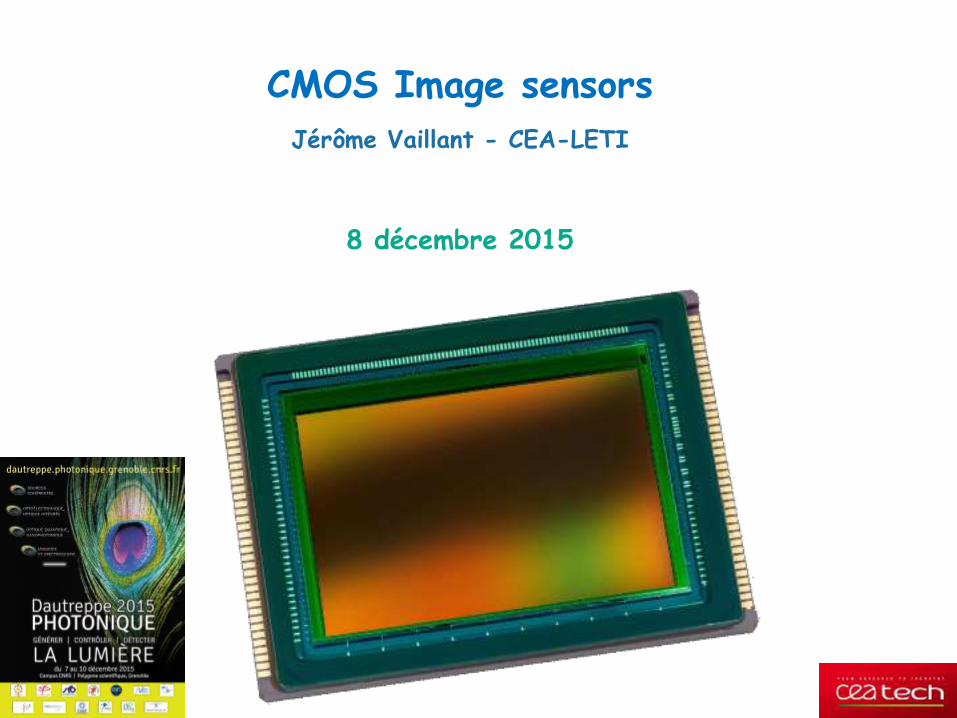
CMOS Image sensors
Jérôme Vaillant - CEA-LETI
8 décembre 2015
| 2Dautreppe 2015 | Vaillant Jérôme | 8 décembre 2015

| 3Dautreppe 2015 | Vaillant Jérôme | 8 décembre 2015
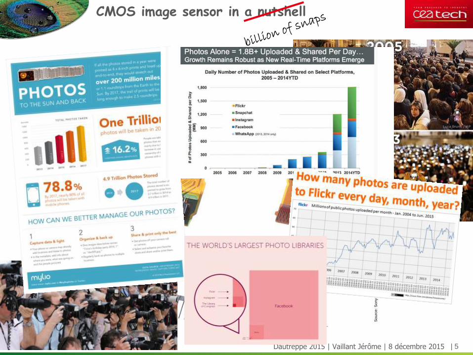
| 5Dautreppe 2015 | Vaillant Jérôme | 8 décembre 2015
CMOS image sensor in a nutshell
So
urc
e: S
on
y

| 6Dautreppe 2015 | Vaillant Jérôme | 8 décembre 2015
• CMOS image sensor today?
• How does it works?
• What’s next?
What’s CMOS image sensor?
| 7Dautreppe 2015 | Vaillant Jérôme | 8 décembre 2015
• CMOS image sensor today? Brief history Market share / main players
• How does it works?
• What’s next?
What’s CMOS image sensor?
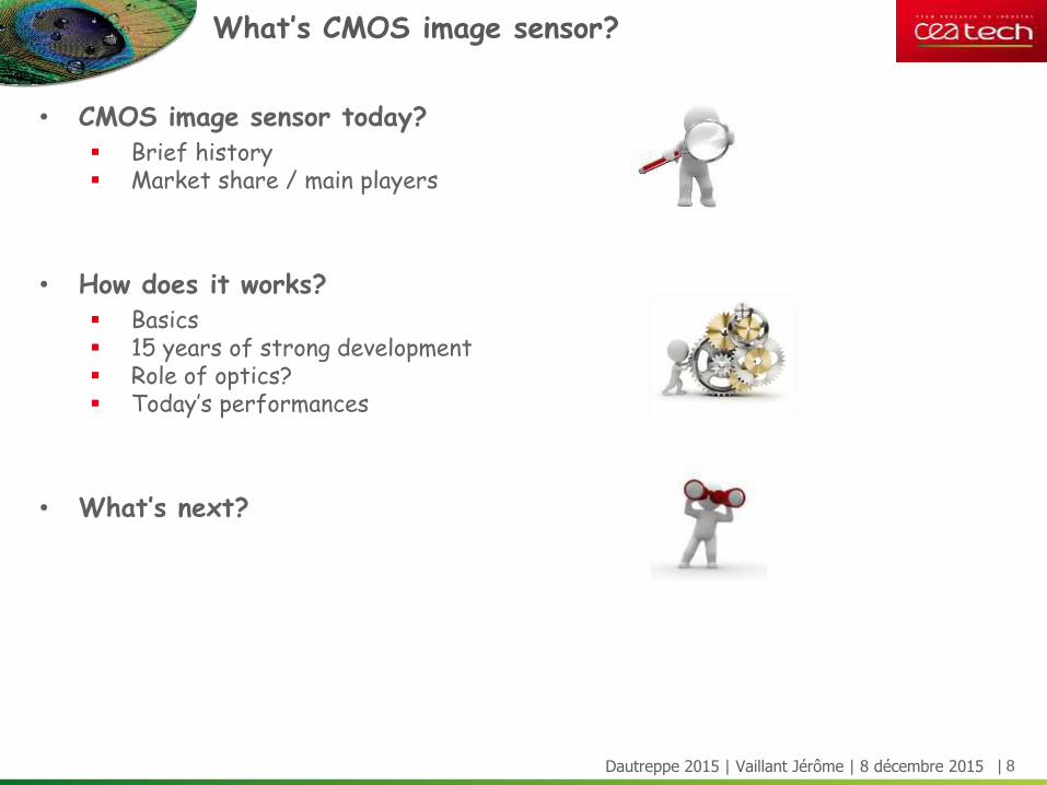
| 8Dautreppe 2015 | Vaillant Jérôme | 8 décembre 2015
• CMOS image sensor today? Brief history Market share / main players
• How does it works? Basics 15 years of strong development Role of optics? Today’s performances
• What’s next?
What’s CMOS image sensor?
| 9Dautreppe 2015 | Vaillant Jérôme | 8 décembre 2015
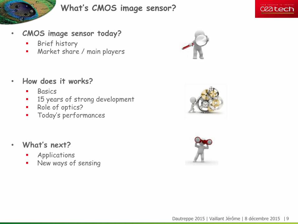
• CMOS image sensor today? Brief history Market share / main players
• How does it works? Basics 15 years of strong development Role of optics? Today’s performances
• What’s next? Applications New ways of sensing
What’s CMOS image sensor?

| 10Dautreppe 2015 | Vaillant Jérôme | 8 décembre 2015
• CMOS image sensor today? Brief history Market share / main players
• How does it works? Basics 15 years of strong development Role of optics? Today’s performances
• What’s next? Applications New ways of sensing
What’s CMOS image sensor?
| 11Dautreppe 2015 | Vaillant Jérôme | 8 décembre 2015
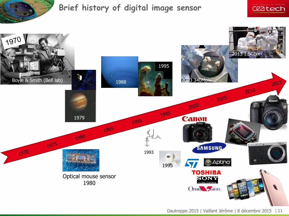
Brief history of digital image sensor
Boyle & Smith (Bell lab)
Optical mouse sensor1980
1988
1995
2003 340Mpix
1979
1995
1993
2013 1.5Gpix
| 12Dautreppe 2015 | Vaillant Jérôme | 8 décembre 2015
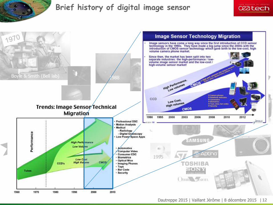
Brief history of digital image sensor
| 13Dautreppe 2015 | Vaillant Jérôme | 8 décembre 2015
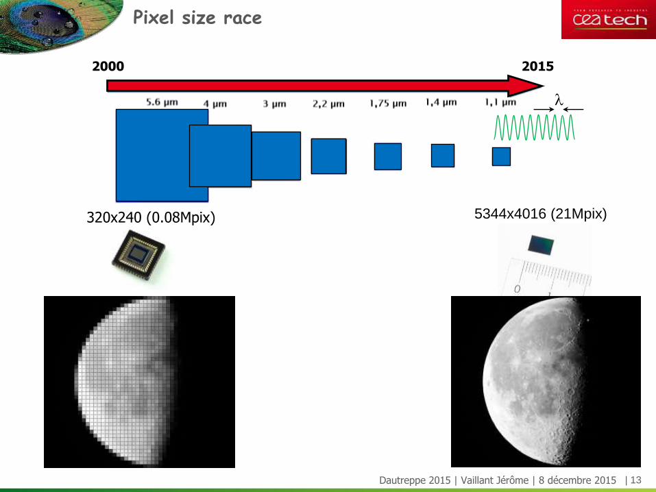
Pixel size race
2000 2015
320x240 (0.08Mpix) 5344x4016 (21Mpix)
| 14Dautreppe 2015 | Vaillant Jérôme | 8 décembre 2015
• CMOS image sensor today? Brief history Market share / main players
• How does it works? Basics 15 years of strong development Role of optics? Today’s performances
• What’s next? Applications New ways of sensing
What’s CMOS image sensor?
| 15Dautreppe 2015 | Vaillant Jérôme | 8 décembre 2015
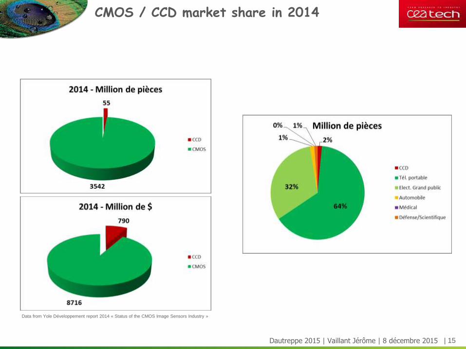
CMOS / CCD market share in 2014
Data from Yole Développement report 2014 « Status of the CMOS Image Sensors Industry »

| 16Dautreppe 2015 | Vaillant Jérôme | 8 décembre 2015
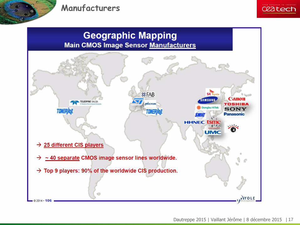
Vendors
| 17Dautreppe 2015 | Vaillant Jérôme | 8 décembre 2015
Manufacturers
| 18Dautreppe 2015 | Vaillant Jérôme | 8 décembre 2015
• CMOS image sensor today? Brief history Market share / main players
• How does it works? Basics 15 years of strong development Role of optics? Today’s performances
• What’s next? Applications New ways of sensing
What’s CMOS image sensor?
| 19Dautreppe 2015 | Vaillant Jérôme | 8 décembre 2015
• CMOS image sensor today? Brief history Market share / main players
• How does it works? Basics 15 years of strong development Role of optics? Today’s performances
• What’s next? Applications New ways of sensing
What’s CMOS image sensor?

| 20Dautreppe 2015 | Vaillant Jérôme | 8 décembre 2015
Camera module teardown
What we are taking about today
| 21Dautreppe 2015 | Vaillant Jérôme | 8 décembre 2015
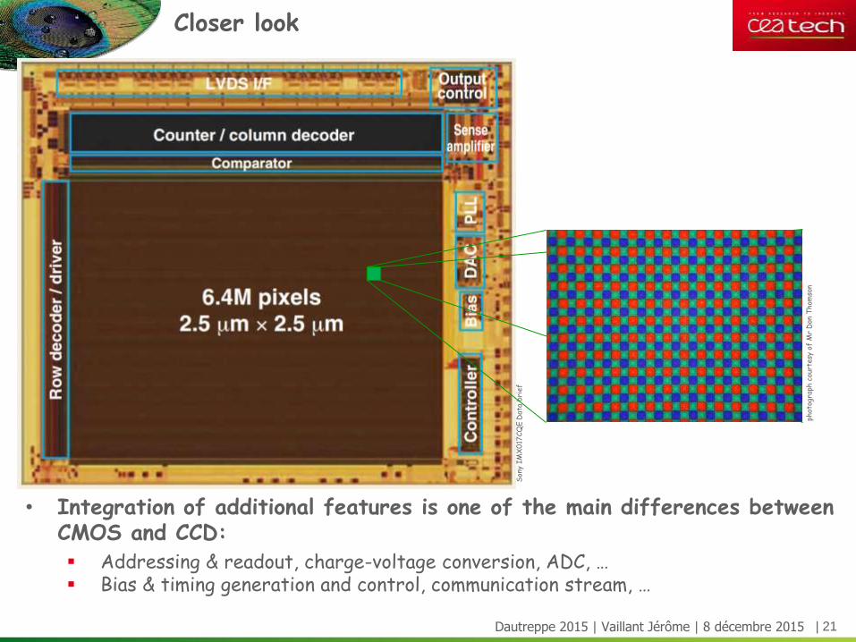
• Integration of additional features is one of the main differences between CMOS and CCD: Addressing & readout, charge-voltage conversion, ADC, … Bias & timing generation and control, communication stream, …
Closer look
Son
y IM
X0
17C
QE
Dat
a b
rief
phot
ogra
ph c
ourt
esy
of M
rD
on T
hom
son
| 22Dautreppe 2015 | Vaillant Jérôme | 8 décembre 2015
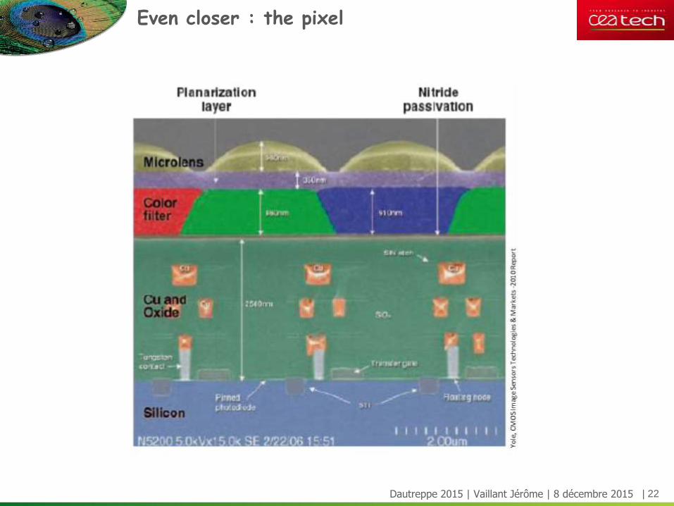
Even closer : the pixel
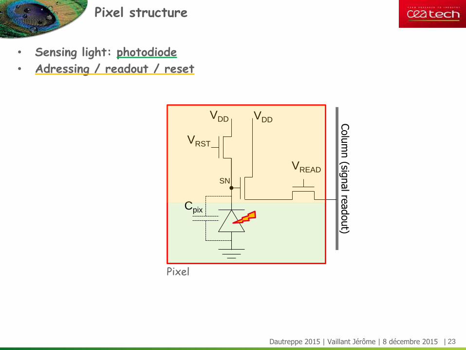
| 23Dautreppe 2015 | Vaillant Jérôme | 8 décembre 2015
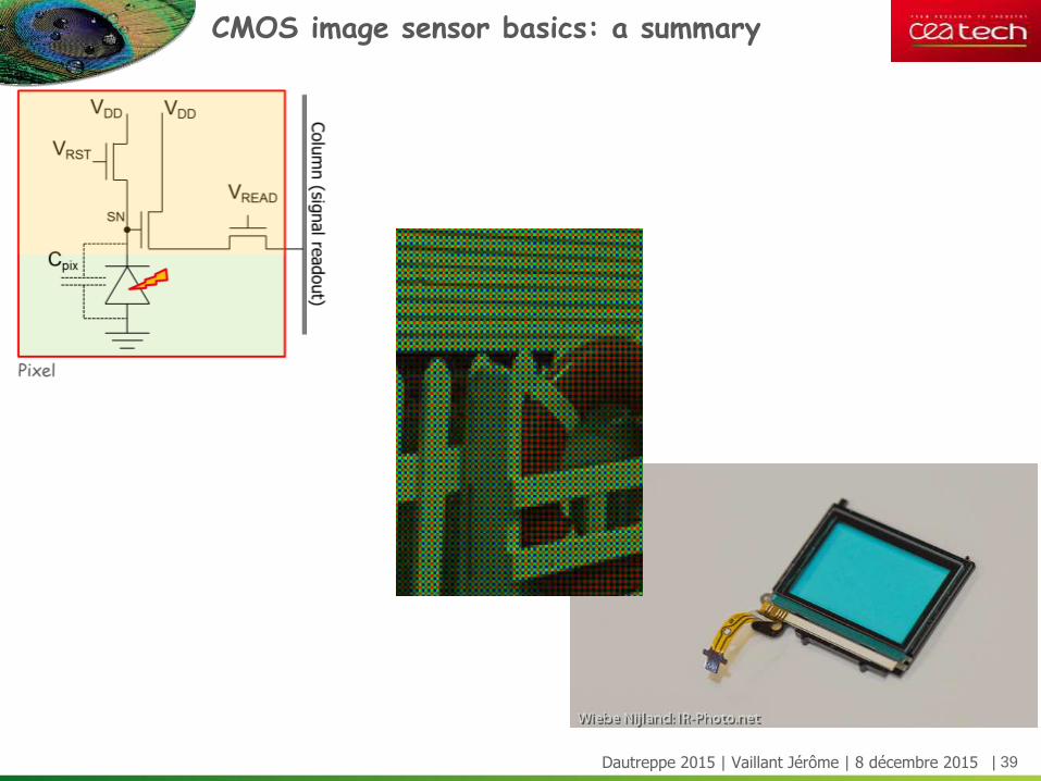
• Sensing light: photodiode
• Adressing / readout / reset
Pixel structure
VREAD
VDD
VRST
VDD
Cpix
SN
Pixel
Colu
mn (sig
nal re
adout)
| 24Dautreppe 2015 | Vaillant Jérôme | 8 décembre 2015
How does it works?
t
V
VRST
VREAD
V
V+ + +
- - -
VREAD
VDD
VRST
VDD
VCOL
| 25Dautreppe 2015 | Vaillant Jérôme | 8 décembre 2015
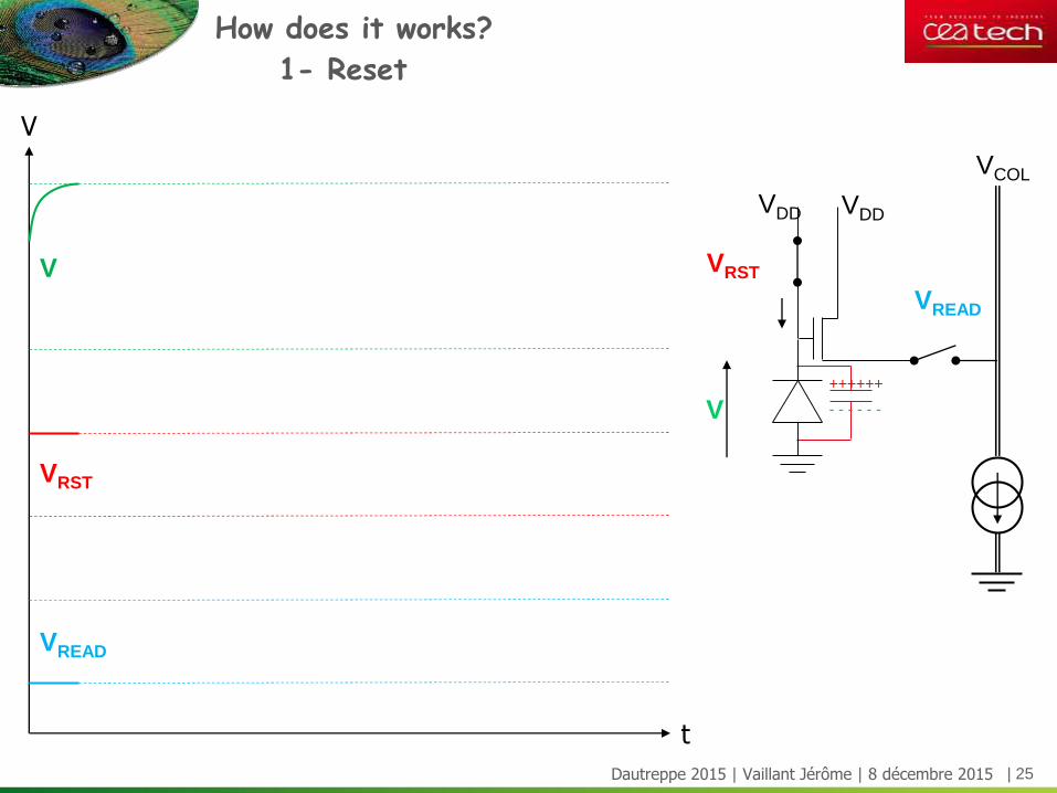
How does it works?
1- Reset
t
V
VRST
VREAD
V
V++++++
- - - - - -
VREAD
VDD
VRST
VDD
VCOL
| 26Dautreppe 2015 | Vaillant Jérôme | 8 décembre 2015
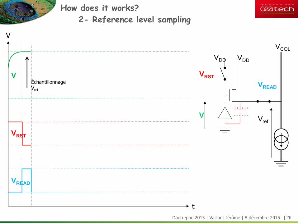
How does it works?
2- Reference level sampling
t
V
VRST
VREAD
VÉchantillonnageVref
V++++++
- - - - - -
VREAD
VDD
VRST
VDD
VCOL
Vref
| 27Dautreppe 2015 | Vaillant Jérôme | 8 décembre 2015
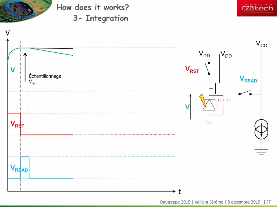
How does it works?
3- Integration
t
V
VRST
VREAD
VÉchantillonnageVref
V+++ ++
- - - - -
VREAD
VDD
VRST
VDD
VCOL

| 28Dautreppe 2015 | Vaillant Jérôme | 8 décembre 2015
How does it works?
3- Integration
t
V
VRST
VREAD
VÉchantillonnageVref
V+ +
- -
VREAD
VDD
VRST
VDD
VCOL
| 29Dautreppe 2015 | Vaillant Jérôme | 8 décembre 2015
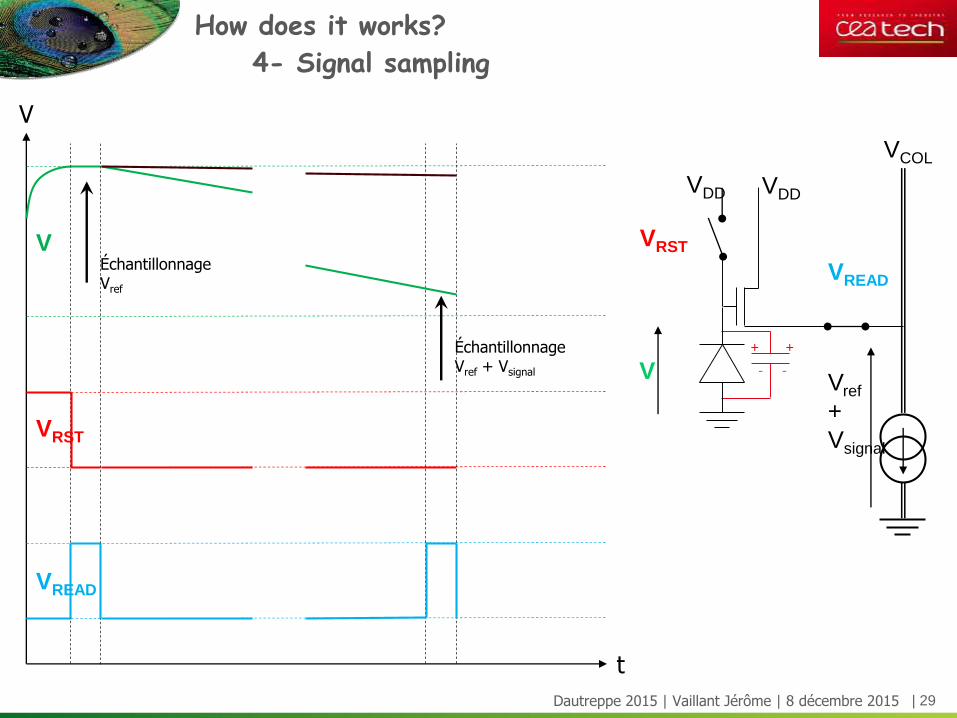
How does it works?
4- Signal sampling
t
V
VRST
VREAD
VÉchantillonnageVref
ÉchantillonnageVref + Vsignal V
+ +
- -
VREAD
VDD
VRST
VDD
VCOL
Vref
+
Vsignal
| 30Dautreppe 2015 | Vaillant Jérôme | 8 décembre 2015
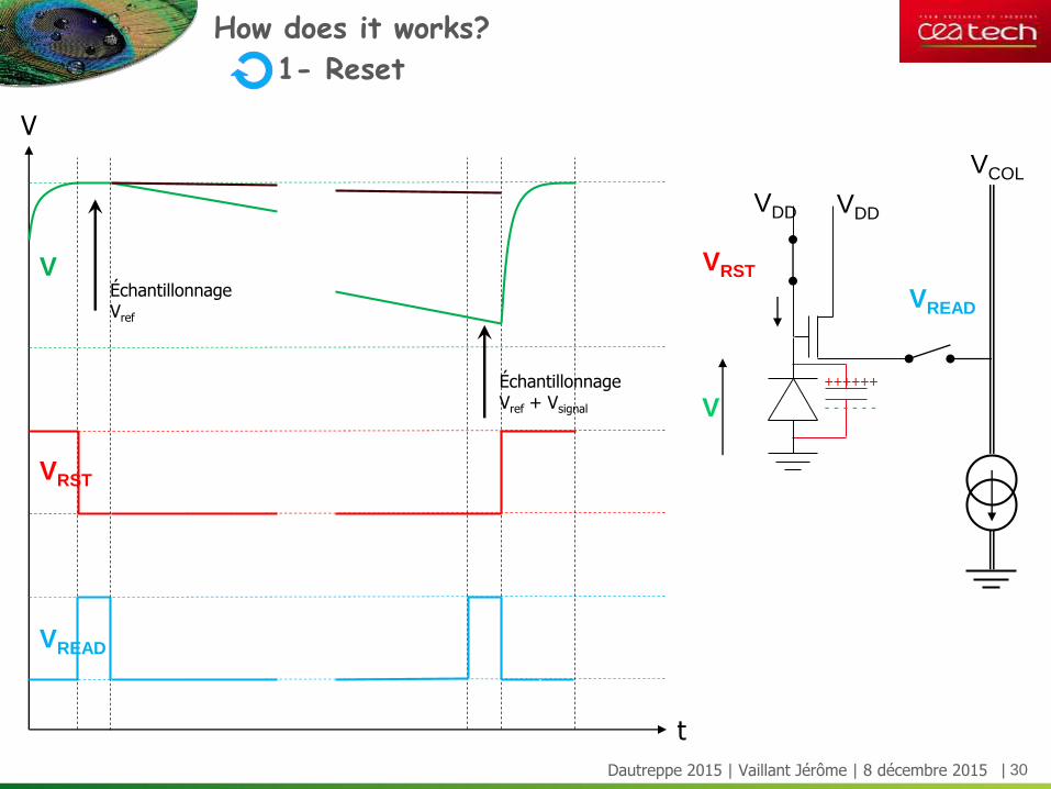
How does it works?
1- Reset
t
V
VRST
VREAD
VÉchantillonnageVref
ÉchantillonnageVref + Vsignal V
++++++
- - - - - -
VREAD
VDD
VRST
VDD
VCOL
| 31Dautreppe 2015 | Vaillant Jérôme | 8 décembre 2015
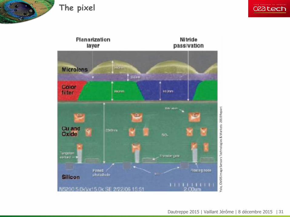
The pixel
| 32Dautreppe 2015 | Vaillant Jérôme | 8 décembre 2015
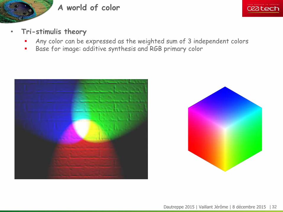
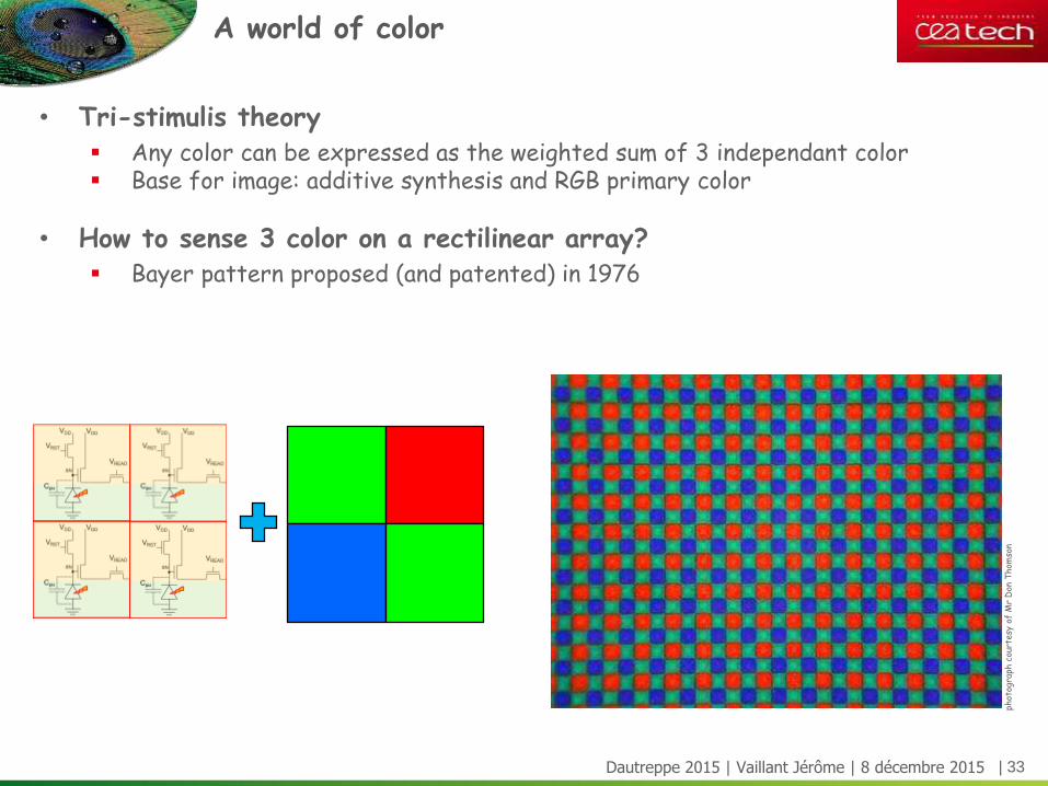
• Tri-stimulis theory Any color can be expressed as the weighted sum of 3 independent colors Base for image: additive synthesis and RGB primary color
A world of color
| 33Dautreppe 2015 | Vaillant Jérôme | 8 décembre 2015
• Tri-stimulis theory Any color can be expressed as the weighted sum of 3 independant color Base for image: additive synthesis and RGB primary color
• How to sense 3 color on a rectilinear array? Bayer pattern proposed (and patented) in 1976
A world of color
phot
ogra
ph c
ourt
esy
of M
rD
on T
hom
son
| 34Dautreppe 2015 | Vaillant Jérôme | 8 décembre 2015
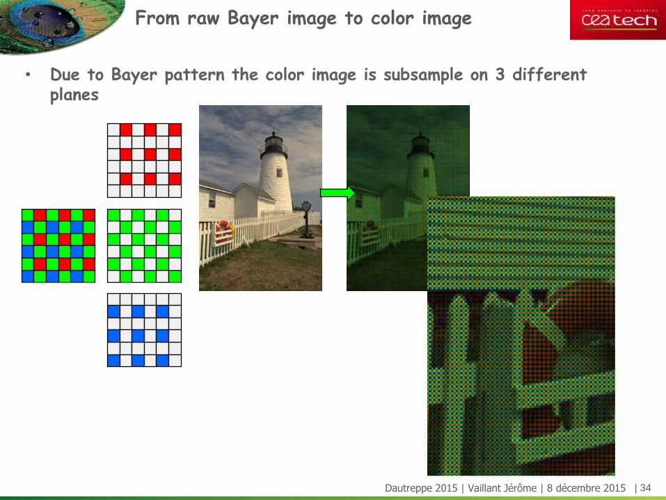
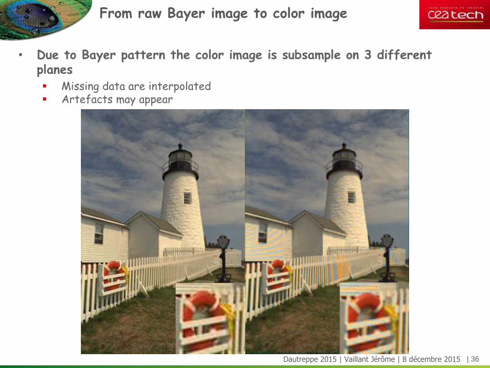
• Due to Bayer pattern the color image is subsample on 3 different planes
From raw Bayer image to color image
| 35Dautreppe 2015 | Vaillant Jérôme | 8 décembre 2015
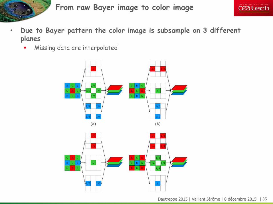
• Due to Bayer pattern the color image is subsample on 3 different planes Missing data are interpolated
From raw Bayer image to color image
| 36Dautreppe 2015 | Vaillant Jérôme | 8 décembre 2015
• Due to Bayer pattern the color image is subsample on 3 different planes Missing data are interpolated Artefacts may appear
From raw Bayer image to color image
| 37Dautreppe 2015 | Vaillant Jérôme | 8 décembre 2015
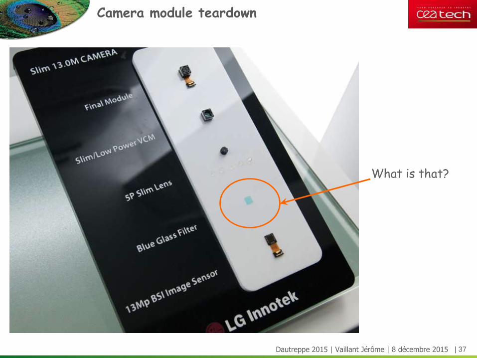
Camera module teardown
What is that?
| 38
htt
p://
ww
w.a
stro
surf
.com
/bui
l/3
50
d/3
50
d.h
tm
Dautreppe 2015 | Vaillant Jérôme | 8 décembre 2015
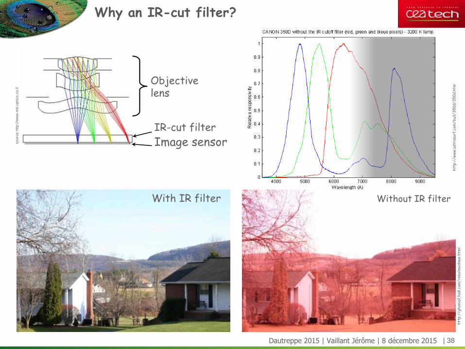
Why an IR-cut filter?so
urc
e h
ttp
://w
ww
.md
-op
tics.c
o.il
IR-cut filter
Objectivelens
Image sensor
With IR filter Without IR filter
htt
p://
ghon
is2
.ho8
.com
/reb
elm
odne
w.h
tml
| 39Dautreppe 2015 | Vaillant Jérôme | 8 décembre 2015
CMOS image sensor basics: a summary

| 40Dautreppe 2015 | Vaillant Jérôme | 8 décembre 2015
• CMOS image sensor today? Brief history Market share / main players
• How does it works? Basics 15 years of strong development Role of optics? Today’s performances
• What’s next? Applications New ways of sensing
What’s CMOS image sensor?
| 41Dautreppe 2015 | Vaillant Jérôme | 8 décembre 2015
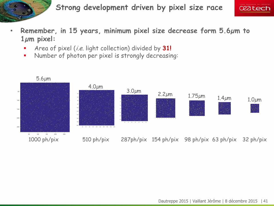
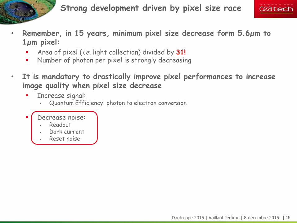
• Remember, in 15 years, minimum pixel size decrease form 5.6µm to 1µm pixel: Area of pixel (i.e. light collection) divided by 31! Number of photon per pixel is strongly decreasing:
Strong development driven by pixel size race
1000 ph/pix 510 ph/pix 287ph/pix 154 ph/pix 98 ph/pix 63 ph/pix 32 ph/pix
5.6µm
4.0µm3.0µm
2.2µm 1.75µm 1.4µm 1.0µm
| 42Dautreppe 2015 | Vaillant Jérôme | 8 décembre 2015
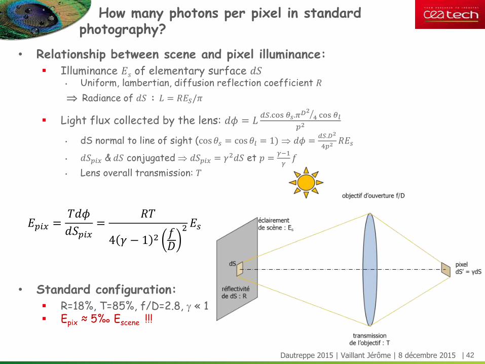
• Relationship between scene and pixel illuminance: Illuminance 𝐸𝑠 of elementary surface 𝑑𝑆
• Uniform, lambertian, diffusion reflection coefficient 𝑅
Radiance of 𝑑𝑆 : 𝐿 = 𝑅𝐸𝑆/𝜋
Light flux collected by the lens: 𝑑𝜙 = 𝐿𝑑𝑆.cos 𝜃𝑠.𝜋 𝐷2
4 cos 𝜃𝑙
𝑝2
• dS normal to line of sight (cos𝜃𝑠 = cos 𝜃𝑙 = 1) 𝑑𝜙 =𝑑𝑆.𝐷2
4𝑝2𝑅𝐸𝑠
• 𝑑𝑆𝑝𝑖𝑥 & 𝑑𝑆 conjugated 𝑑𝑆𝑝𝑖𝑥 = 𝛾2𝑑𝑆 et 𝑝 =𝛾−1
𝛾𝑓
• Lens overall transmission: 𝑇
• Standard configuration: R=18%, T=85%, f/D=2.8, « 1 Epix ≈ 5‰ Escene !!!
How many photons per pixel in standard photography?
𝐸𝑝𝑖𝑥 =𝑇𝑑𝜙
𝑑𝑆𝑝𝑖𝑥=
𝑅𝑇
4 𝛾 − 1 2 𝑓𝐷
2 𝐸𝑠
| 43Dautreppe 2015 | Vaillant Jérôme | 8 décembre 2015
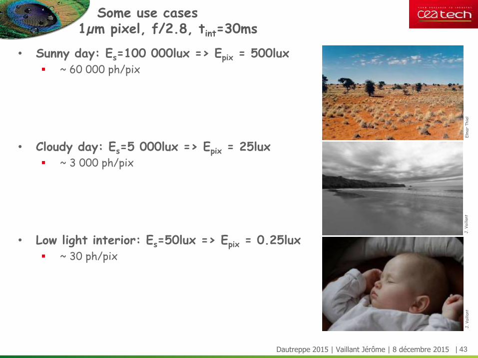
• Sunny day: Es=100 000lux => Epix = 500lux ~ 60 000 ph/pix
• Cloudy day: Es=5 000lux => Epix = 25lux ~ 3 000 ph/pix
• Low light interior: Es=50lux => Epix = 0.25lux ~ 30 ph/pix
Some use cases 1µm pixel, f/2.8, tint=30ms
Elm
arT
hie
lJ
. Vai
llan
tJ
. Vai
llan
t
| 44Dautreppe 2015 | Vaillant Jérôme | 8 décembre 2015
• Remember, in 15 years, minimum pixel size decrease form 5.6µm to 1µm pixel: Area of pixel (i.e. light collection) divided by 31! Number of photon per pixel is strongly decreasing
• It is mandatory to drastically improve pixel performances to increase image quality when pixel size decrease Increase signal:
• Quantum Efficiency: photon to electron conversion
Decrease noise: • Readout• Dark current• Reset noise
Strong development driven by pixel size race
| 45Dautreppe 2015 | Vaillant Jérôme | 8 décembre 2015
• Remember, in 15 years, minimum pixel size decrease form 5.6µm to 1µm pixel: Area of pixel (i.e. light collection) divided by 31! Number of photon per pixel is strongly decreasing
• It is mandatory to drastically improve pixel performances to increase image quality when pixel size decrease Increase signal:
• Quantum Efficiency: photon to electron conversion
Decrease noise: • Readout• Dark current• Reset noise
Strong development driven by pixel size race
| 46Dautreppe 2015 | Vaillant Jérôme | 8 décembre 2015
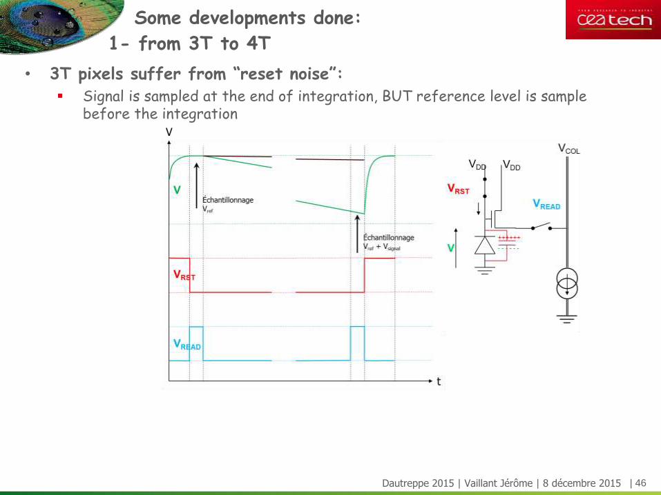
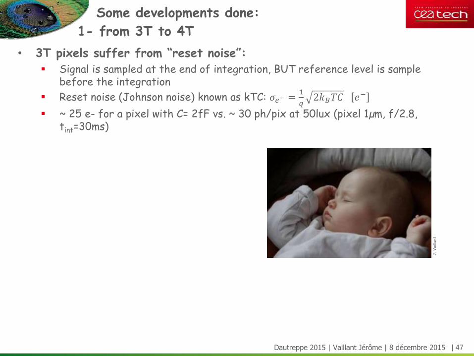
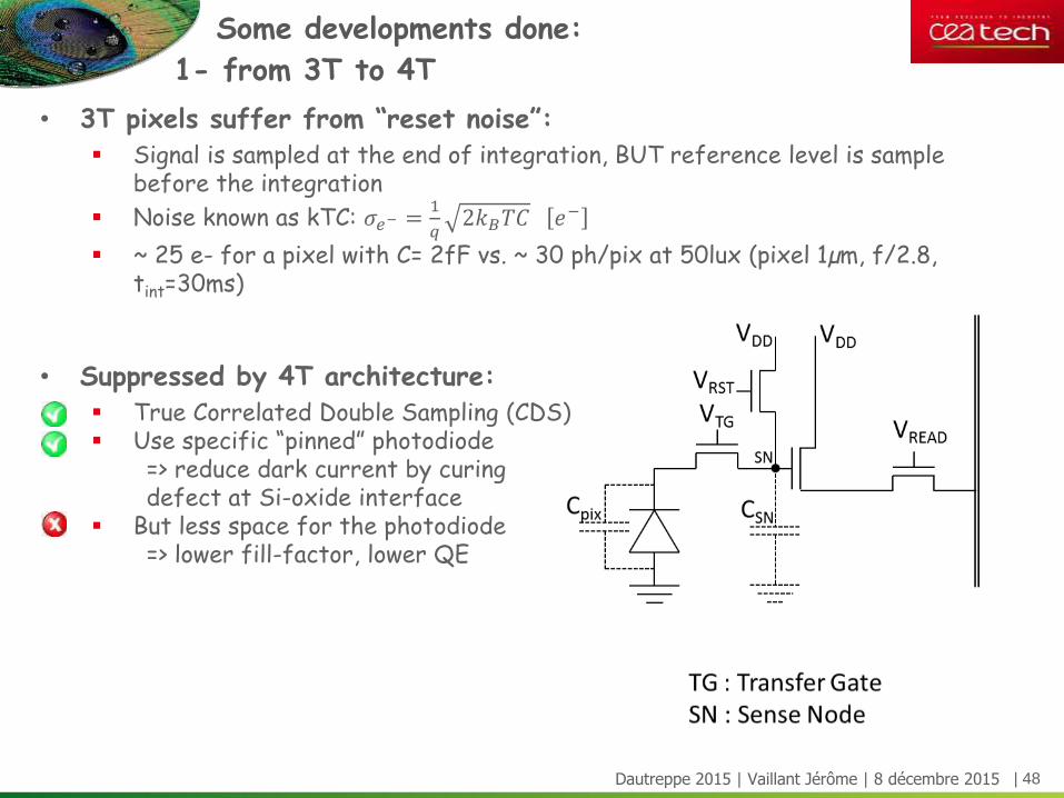
• 3T pixels suffer from “reset noise”: Signal is sampled at the end of integration, BUT reference level is sample
before the integration
Some developments done:
1- from 3T to 4T
| 47
• 3T pixels suffer from “reset noise”: Signal is sampled at the end of integration, BUT reference level is sample
before the integration
Reset noise (Johnson noise) known as kTC: 𝜎𝑒− =1
𝑞2𝑘𝐵𝑇𝐶 𝑒−
~ 25 e- for a pixel with C= 2fF vs. ~ 30 ph/pix at 50lux (pixel 1µm, f/2.8, tint=30ms)
J. V
aillan
t
Dautreppe 2015 | Vaillant Jérôme | 8 décembre 2015
Some developments done:
1- from 3T to 4T
| 48
• 3T pixels suffer from “reset noise”: Signal is sampled at the end of integration, BUT reference level is sample
before the integration
Noise known as kTC: 𝜎𝑒− =1
𝑞2𝑘𝐵𝑇𝐶 𝑒−
~ 25 e- for a pixel with C= 2fF vs. ~ 30 ph/pix at 50lux (pixel 1µm, f/2.8, tint=30ms)
• Suppressed by 4T architecture: True Correlated Double Sampling (CDS) Use specific “pinned” photodiode
=> reduce dark current by curingdefect at Si-oxide interface
But less space for the photodiode => lower fill-factor, lower QE
Dautreppe 2015 | Vaillant Jérôme | 8 décembre 2015
Some developments done:
1- from 3T to 4T
| 49
• 3T pixels suffer from “reset noise”: Signal is sampled at the end of integration, BUT reference level is sample
before the integration
Noise known as kTC: 𝜎𝑒− =1
𝑞2𝑘𝐵𝑇𝐶 𝑒−
~ 25 e- for a pixel with C= 2fF vs. ~ 30 ph/pix at 50lux (pixel 1µm, f/2.8, tint=30ms)
• Suppressed by 4T architecture: Reduce noise Use specific “pinned” photodiode
=> reduce dark current by curingdefect at Si-oxide interface
But less space for the photodiode => lower fill-factor, lower QE
Dautreppe 2015 | Vaillant Jérôme | 8 décembre 2015
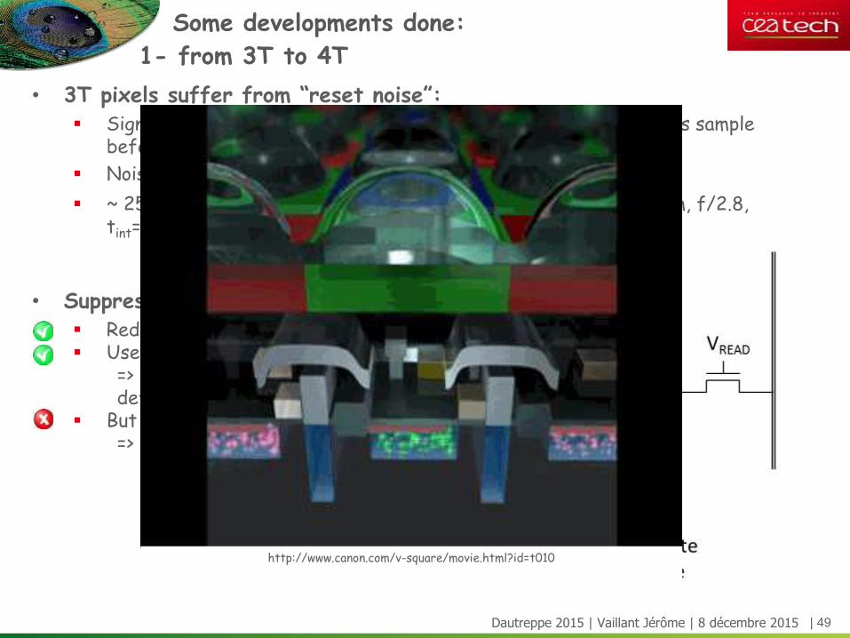
Some developments done:
1- from 3T to 4T
http://www.canon.com/v-square/movie.html?id=t010

| 50Dautreppe 2015 | Vaillant Jérôme | 8 décembre 2015
• Remember, in 15 years, minimum pixel size decrease form 5.6µm to 1µm pixel: Area of pixel (i.e. light collection) divided by 31! Number of photon per pixel is strongly decreasing
• It is mandatory to drastically improve pixel performances to increase image quality when pixel size decrease Increase signal:
• Quantum Efficiency: photon to electron conversion
Decrease noise: • Readout• Dark current• Reset noise
Strong development driven by pixel size race
| 51Dautreppe 2015 | Vaillant Jérôme | 8 décembre 2015
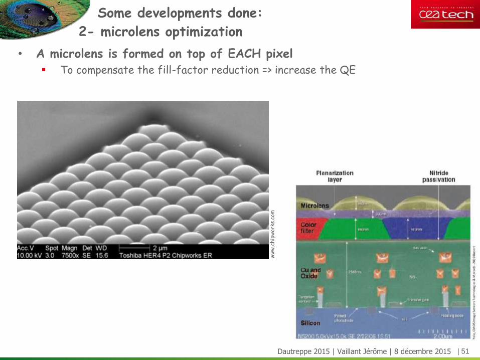
• A microlens is formed on top of EACH pixel To compensate the fill-factor reduction => increase the QE
Some developments done:
2- microlens optimization
ww
w.c
hip
wor
ks.c
om
| 52
ww
w.c
hip
work
s.c
om
Dautreppe 2015 | Vaillant Jérôme | 8 décembre 2015
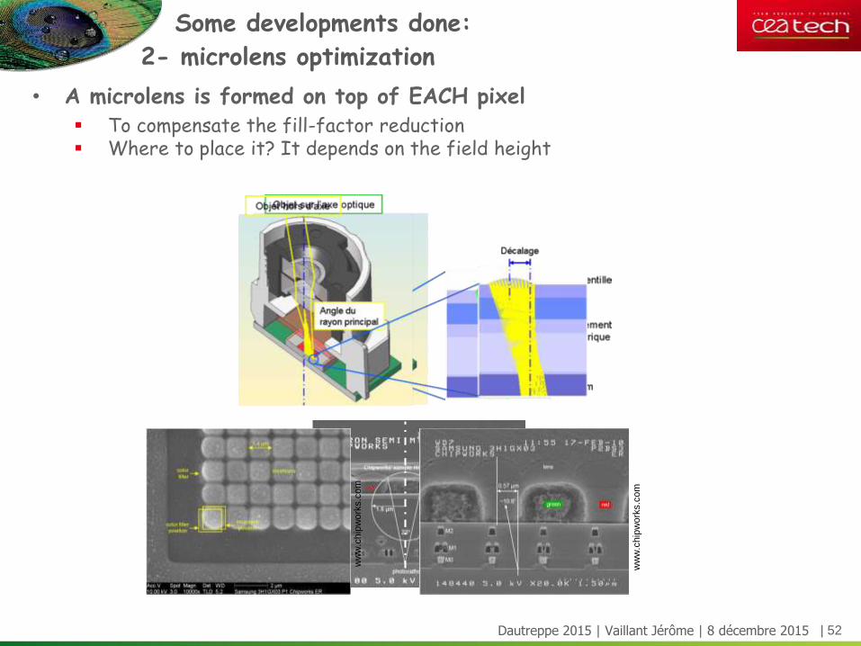
• A microlens is formed on top of EACH pixel To compensate the fill-factor reduction Where to place it? It depends on the field height
Some developments done:
2- microlens optimization
ww
w.c
hip
work
s.c
om
ww
w.c
hip
work
s.c
om
| 53Dautreppe 2015 | Vaillant Jérôme | 8 décembre 2015
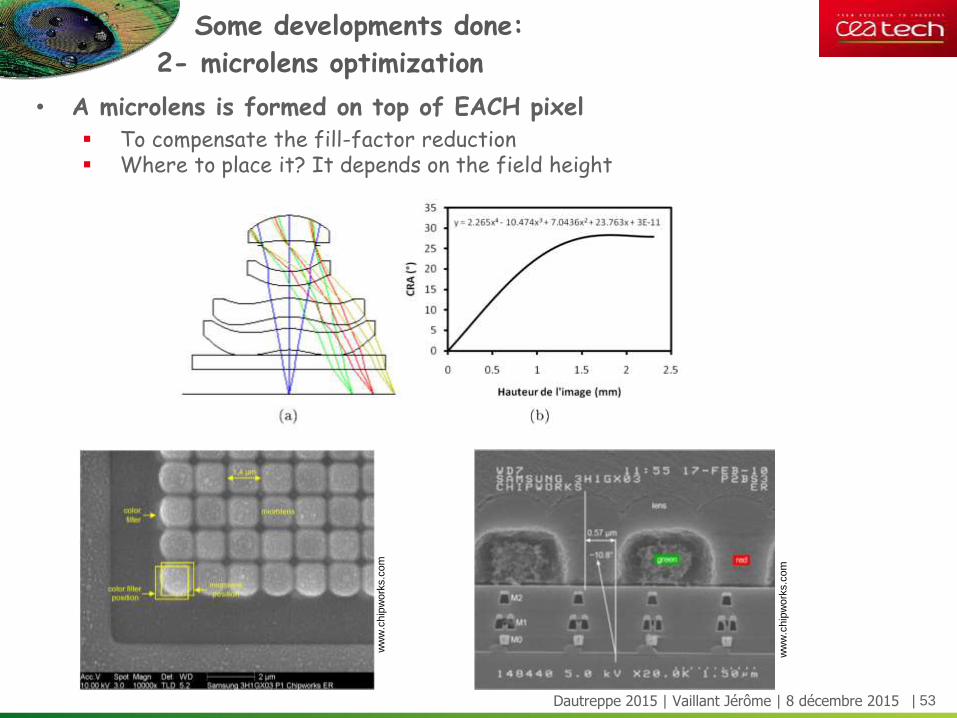
• A microlens is formed on top of EACH pixel To compensate the fill-factor reduction Where to place it? It depends on the field height
Some developments done:
2- microlens optimization
ww
w.c
hip
work
s.c
om
ww
w.c
hip
work
s.c
om
| 54Dautreppe 2015 | Vaillant Jérôme | 8 décembre 2015
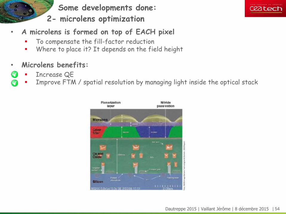
• A microlens is formed on top of EACH pixel To compensate the fill-factor reduction Where to place it? It depends on the field height
• Microlens benefits: Increase QE Improve FTM / spatial resolution by managing light inside the optical stack
Some developments done:
2- microlens optimization
| 55Dautreppe 2015 | Vaillant Jérôme | 8 décembre 2015
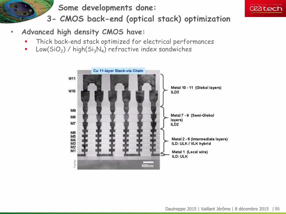
• Advanced high density CMOS have: Thick back-end stack optimized for electrical performances Low(SiO2) / high(Si3N4) refractive index sandwiches
Some developments done:
3- CMOS back-end (optical stack) optimization
Fuj
itsu
| 56Dautreppe 2015 | Vaillant Jérôme | 8 décembre 2015
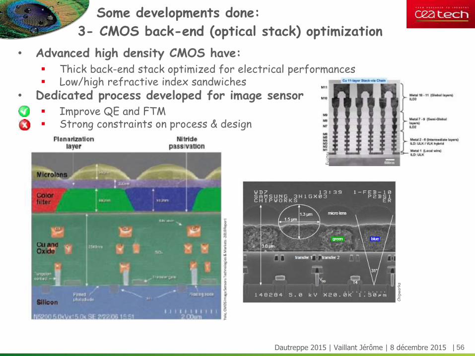
• Advanced high density CMOS have: Thick back-end stack optimized for electrical performances Low/high refractive index sandwiches
• Dedicated process developed for image sensor Improve QE and FTM Strong constraints on process & design
Some developments done:
3- CMOS back-end (optical stack) optimization
Fuj
itsu
Chip
wor
ks
| 57Dautreppe 2015 | Vaillant Jérôme | 8 décembre 2015
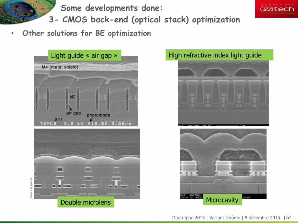
• Other solutions for BE optimization
Some developments done:
3- CMOS back-end (optical stack) optimizationS
ourc
e C
hip
wor
ks
Light guide « air gap » High refractive index light guide
Double microlens Microcavity
| 58Dautreppe 2015 | Vaillant Jérôme | 8 décembre 2015
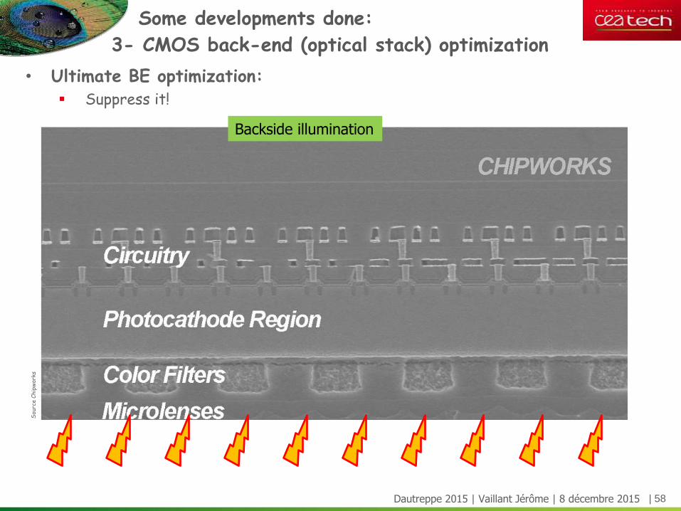
• Ultimate BE optimization: Suppress it!
Some developments done:
3- CMOS back-end (optical stack) optimizationS
ourc
e C
hip
wor
ks
Backside illumination

| 59Dautreppe 2015 | Vaillant Jérôme | 8 décembre 2015
• CMOS image sensor today? Brief history Market share / main players
• How does it works? Basics 15 years of strong development Role of optics? Today’s performances
• What’s next? Applications New ways of sensing
What’s CMOS image sensor?
| 60Dautreppe 2015 | Vaillant Jérôme | 8 décembre 2015
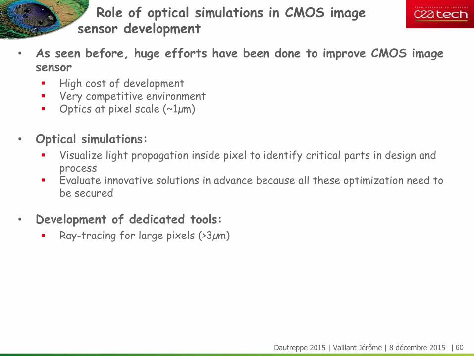
• As seen before, huge efforts have been done to improve CMOS image sensor High cost of development Very competitive environment Optics at pixel scale (~1µm)
• Optical simulations: Visualize light propagation inside pixel to identify critical parts in design and
process Evaluate innovative solutions in advance because all these optimization need to
be secured
• Development of dedicated tools: Ray-tracing for large pixels (>3µm)
Role of optical simulations in CMOS image sensor development
| 61Dautreppe 2015 | Vaillant Jérôme | 8 décembre 2015
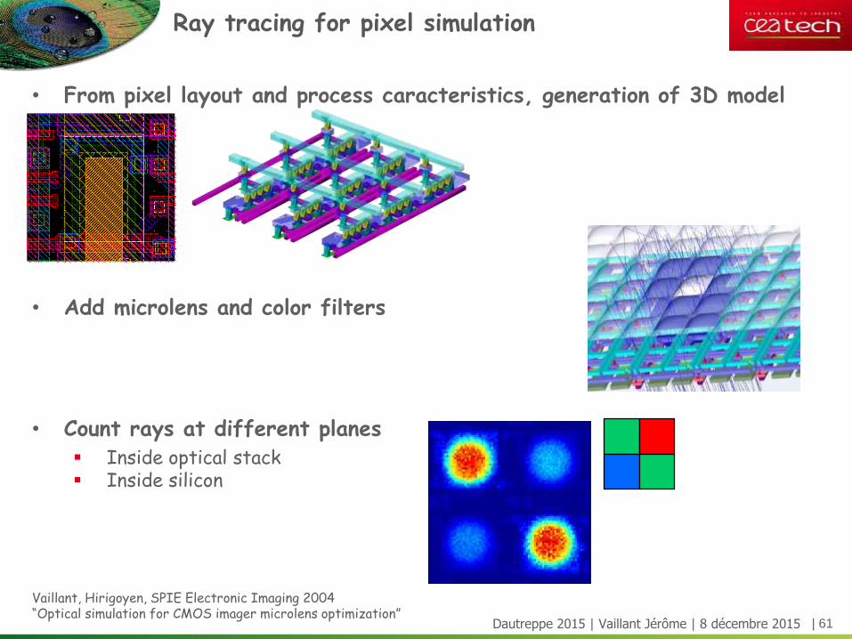
• From pixel layout and process caracteristics, generation of 3D model
• Add microlens and color filters
• Count rays at different planes Inside optical stack Inside silicon
Ray tracing for pixel simulation
Vaillant, Hirigoyen, SPIE Electronic Imaging 2004 “Optical simulation for CMOS imager microlens optimization”

| 62Dautreppe 2015 | Vaillant Jérôme | 8 décembre 2015
• As seen before, huge efforts have been done to improve CMOS image sensor High cost of development Very competitive environment Optics at pixel scale (~1µm)
• Optical simulations: Visualize light propagation inside pixel to identify critical parts in design and
process Evaluate innovative solutions in advance because all these optimization need to
be secured
• Development of dedicated tools: Ray-tracing for large pixels (>3µm) Electromagnetic simulations using FDTD below 3µm
Role of optical simulations in CMOS image sensor development
| 63Dautreppe 2015 | Vaillant Jérôme | 8 décembre 2015
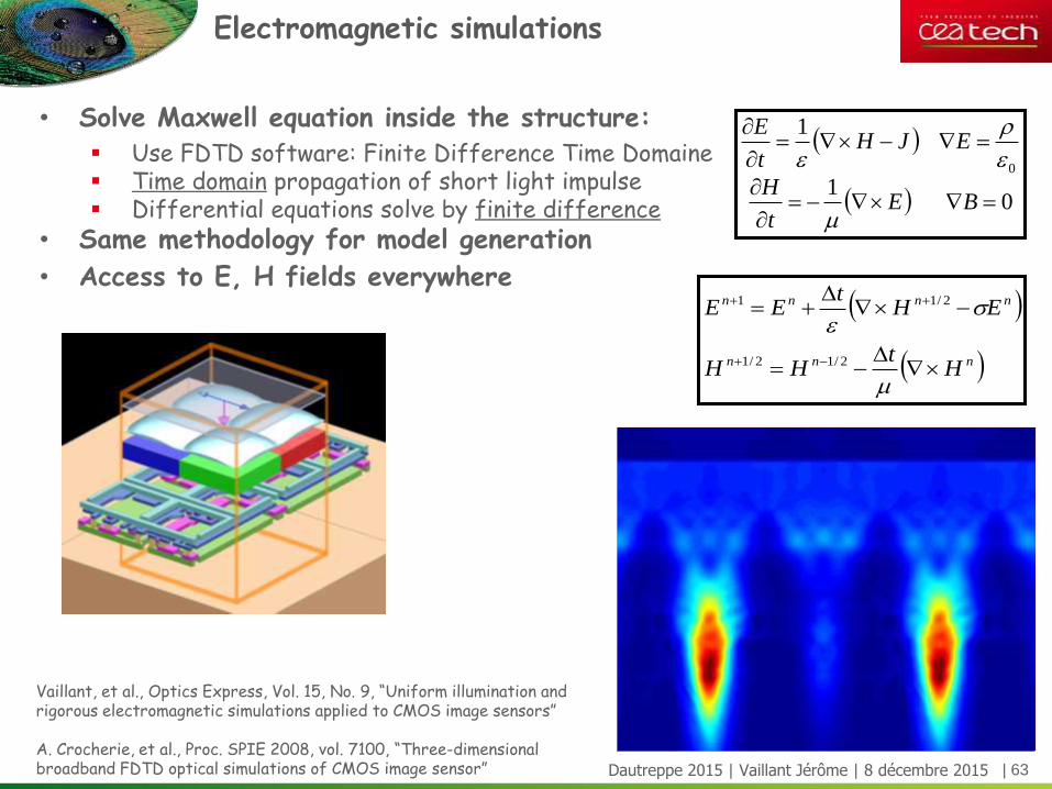
• Solve Maxwell equation inside the structure: Use FDTD software: Finite Difference Time Domaine Time domain propagation of short light impulse Differential equations solve by finite difference
• Same methodology for model generation
• Access to E, H fields everywhere
Electromagnetic simulations
01
1
0
BEt
H
EJHt
E
nnn
nnnn
Ht
HH
EHt
EE
2/12/1
2/11
Vaillant, et al., Optics Express, Vol. 15, No. 9, “Uniform illumination and rigorous electromagnetic simulations applied to CMOS image sensors”
A. Crocherie, et al., Proc. SPIE 2008, vol. 7100, “Three-dimensional broadband FDTD optical simulations of CMOS image sensor”

| 64Dautreppe 2015 | Vaillant Jérôme | 8 décembre 2015
• As seen before, huge efforts have been done to improve CMOS image sensor High cost of development Very competitive environment Optics at pixel scale (~1µm)
• Optical simulations: Visualize light propagation inside pixel to identify critical parts in design and
process Evaluate innovative solutions in advance because all these optimization need to
be secured
• Development of dedicated tools: Ray-tracing for large pixels (>3µm) Electromagnetic simulations using FDTD below 3µm Opto-electrical simulation flow
Role of optical simulations in CMOS image sensor development
| 65Dautreppe 2015 | Vaillant Jérôme | 8 décembre 2015
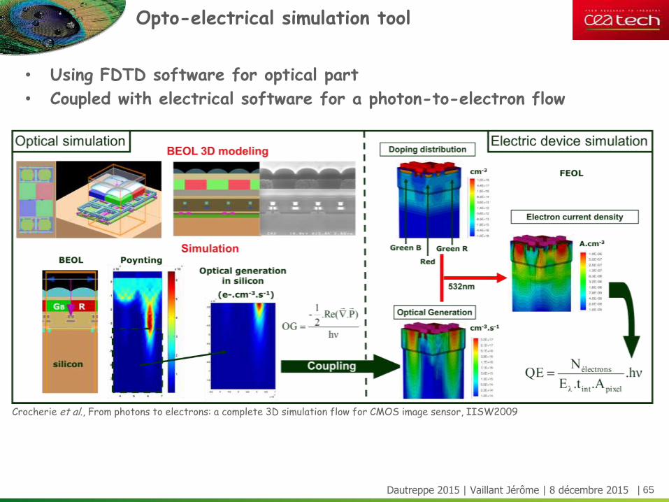
• Using FDTD software for optical part
• Coupled with electrical software for a photon-to-electron flow
Opto-electrical simulation tool
Crocherie et al., From photons to electrons: a complete 3D simulation flow for CMOS image sensor, IISW2009
| 66Dautreppe 2015 | Vaillant Jérôme | 8 décembre 2015
• CMOS image sensor today? Brief history Market share / main players
• How does it works? Basics 15 years of strong development Role of optics? Today’s performances
• What’s next? Applications New ways of sensing
What’s CMOS image sensor?
| 67Dautreppe 2015 | Vaillant Jérôme | 8 décembre 2015
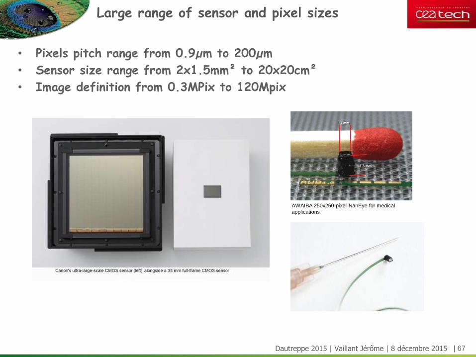
• Pixels pitch range from 0.9µm to 200µm
• Sensor size range from 2x1.5mm² to 20x20cm²
• Image definition from 0.3MPix to 120Mpix
Large range of sensor and pixel sizes
AWAIBA 250x250-pixel NanEye for medical
applications
| 68Dautreppe 2015 | Vaillant Jérôme | 8 décembre 2015
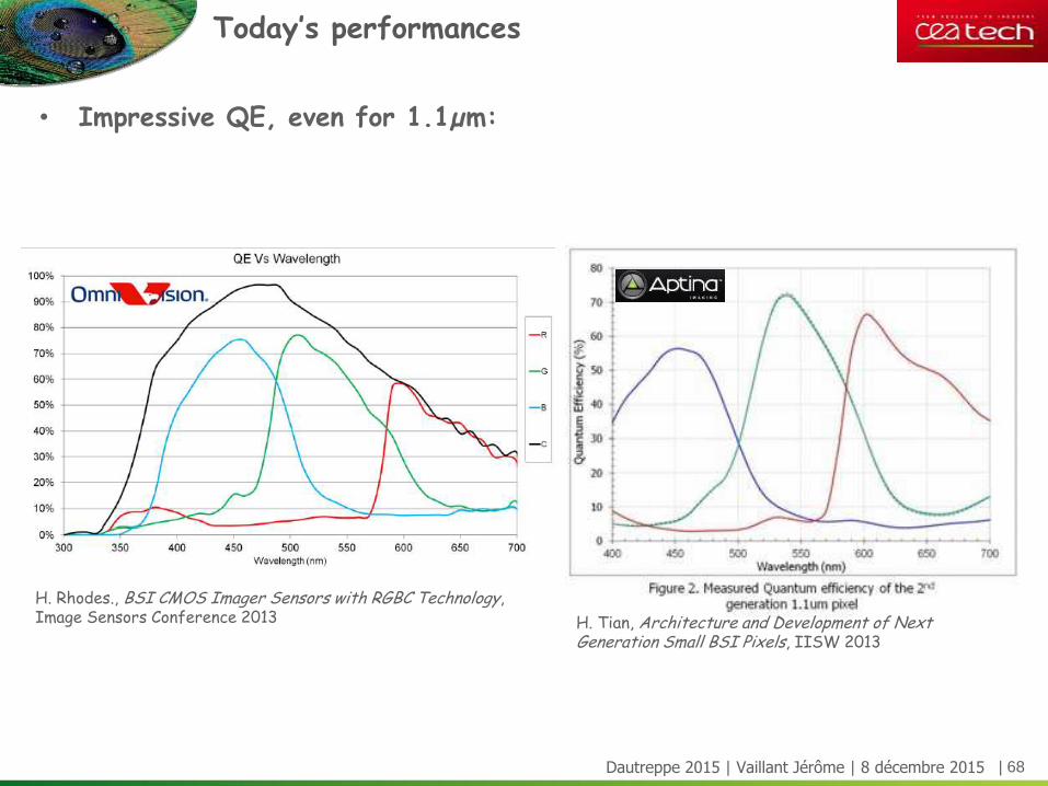
• Impressive QE, even for 1.1µm:
Today’s performances
H. Tian, Architecture and Development of Next Generation Small BSI Pixels, IISW 2013
H. Rhodes., BSI CMOS Imager Sensors with RGBC Technology,Image Sensors Conference 2013
| 69Dautreppe 2015 | Vaillant Jérôme | 8 décembre 2015
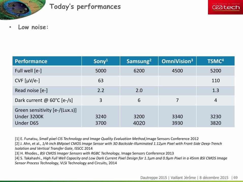
• Low noise:
Today’s performances
Performance Sony1 Samsung2 OmniVision3 TSMC4
Full well [e-] 5000 6200 4500 5200
CVF [µV/e-] 63 110
Read noise [e-] 2.2 2.0 1.3
Dark current @ 60°C [e-/s] 3 6 7 4
Green sensitivity [e-/(Lux.s)]Under 3200KUnder D65
32403700
32004020
33403930
32303820
[1] E. Funatsu, Small pixel CIS Technology and Image Quality Evaluation Method,Image Sensors Conference 2012[2] J. Ahn, et al., 1/4-inch 8Mpixel CMOS Image Sensor with 3D Backside-Illuminated 1.12μm Pixel with Front-Side Deep-Trench Isolation and Vertical Transfer Gate, ISSCC 2014[3] H. Rhodes., BSI CMOS Imager Sensors with RGBC Technology, Image Sensors Conference 2013[4] S. Takahashi., High Full Well Capacity and Low Dark Current Pixel Design for 1.1µm and 0.9µm Pixel in a 45nm BSI CMOS Image Sensor Process Technology, VLSI Technology and Circuits, 2014

| 70Dautreppe 2015 | Vaillant Jérôme | 8 décembre 2015
• CMOS image sensor today? Brief history Market share / main players
• How does it works? Basics 15 years of strong development Today’s performances
• What’s next? Applications New ways of sensing
What’s CMOS image sensor?
| 71
Consumer
Professional
Dautreppe 2015 | Vaillant Jérôme | 8 décembre 2015
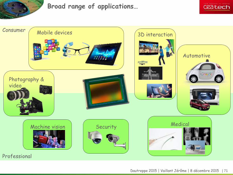
Broad range of applications…
Mobile devices
Photography & video
Security Medical
Automotive
Machine vision
3D interaction
| 72Dautreppe 2015 | Vaillant Jérôme | 8 décembre 2015
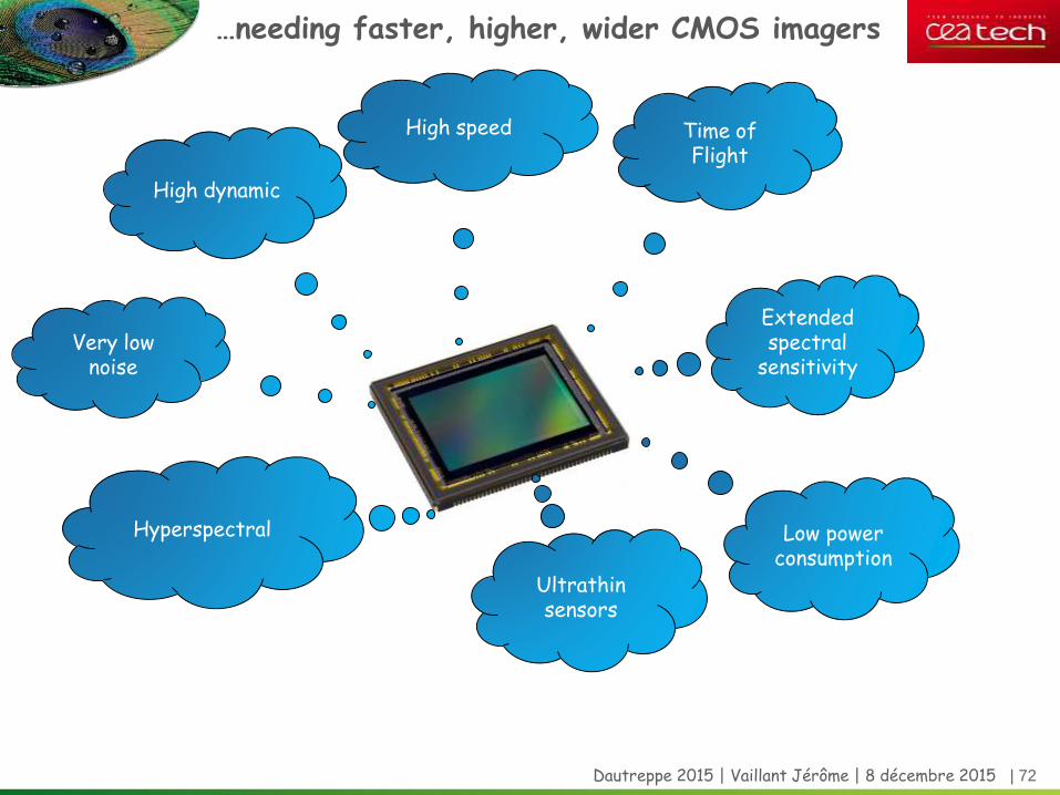
…needing faster, higher, wider CMOS imagers
High dynamic
Ultrathin sensors
Hyperspectral
Extended spectral
sensitivityVery low
noise
High speed Time of Flight
Low power consumption
| 73Dautreppe 2015 | Vaillant Jérôme | 8 décembre 2015
• CMOS image sensor today? Brief history Market share / main players
• How does it works? Basics 15 years of strong development Today’s performances
• What’s next? Applications New ways of sensing
What’s CMOS image sensor?
| 74Dautreppe 2015 | Vaillant Jérôme | 8 décembre 2015
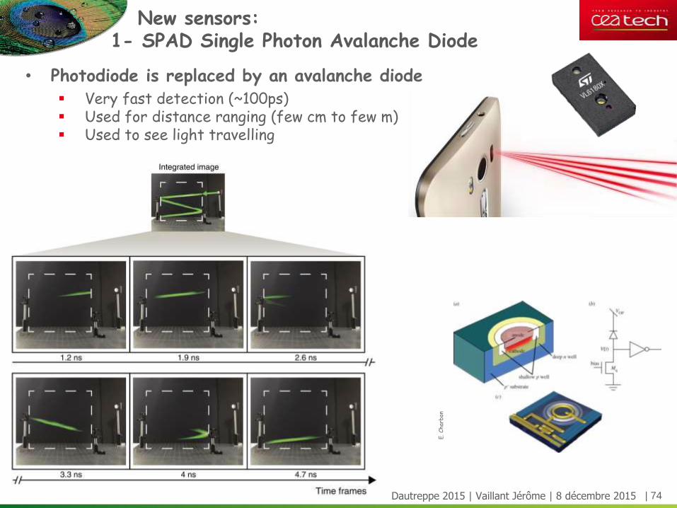
• Photodiode is replaced by an avalanche diode Very fast detection (~100ps) Used for distance ranging (few cm to few m) Used to see light travelling
New sensors:1- SPAD Single Photon Avalanche Diode
E. C
har
bon
| 75Dautreppe 2015 | Vaillant Jérôme | 8 décembre 2015
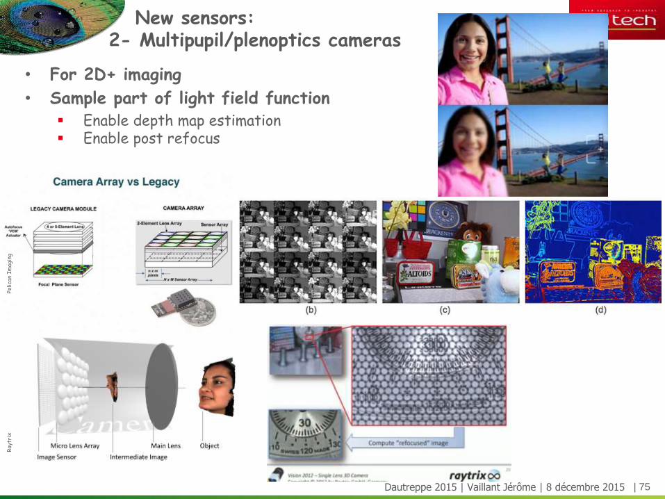
• For 2D+ imaging
• Sample part of light field function Enable depth map estimation Enable post refocus
New sensors:2- Multipupil/plenoptics cameras
Pelica
nIm
agin
gR
aytr
ix
| 76Dautreppe 2015 | Vaillant Jérôme | 8 décembre 2015
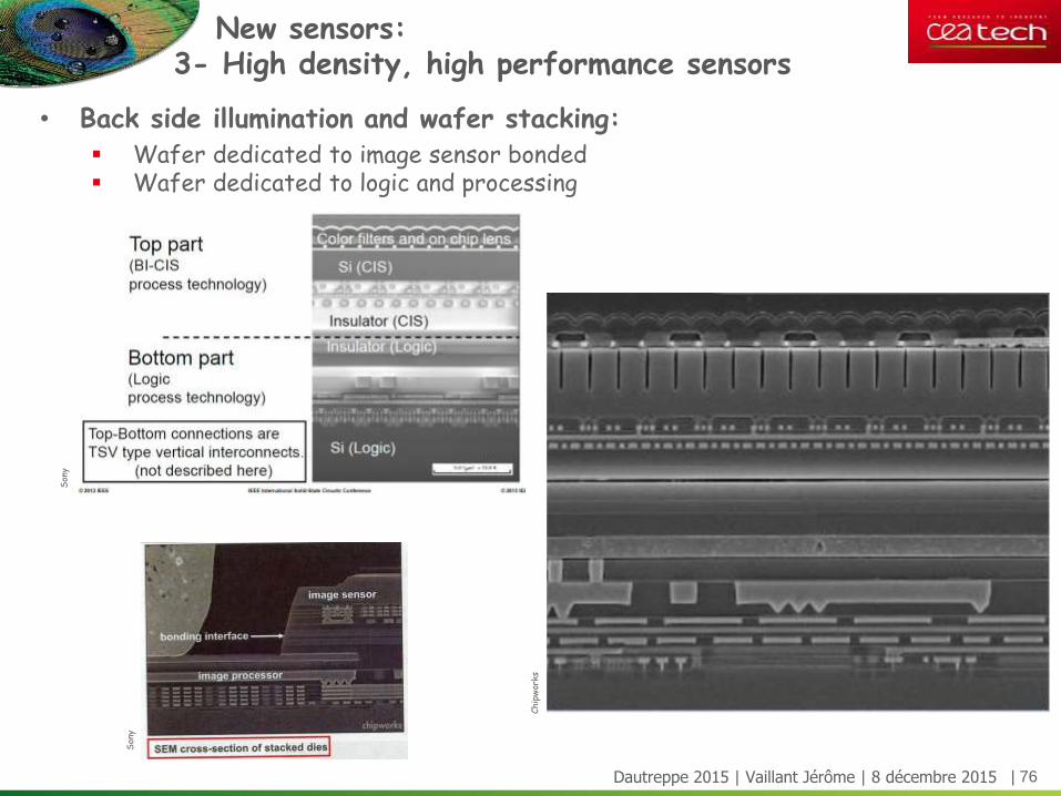
• Back side illumination and wafer stacking: Wafer dedicated to image sensor bonded Wafer dedicated to logic and processing
New sensors:3- High density, high performance sensors
Son
y
Son
y
Chip
wor
ks
| 77Dautreppe 2015 | Vaillant Jérôme | 8 décembre 2015
Thank you for your attention
Any question?
So
urc
e: S
on
y