Embed Size (px)
Citation preview
Communications Baseband PDR
Communications Baseband
Project 05500
Communications Baseband PDR
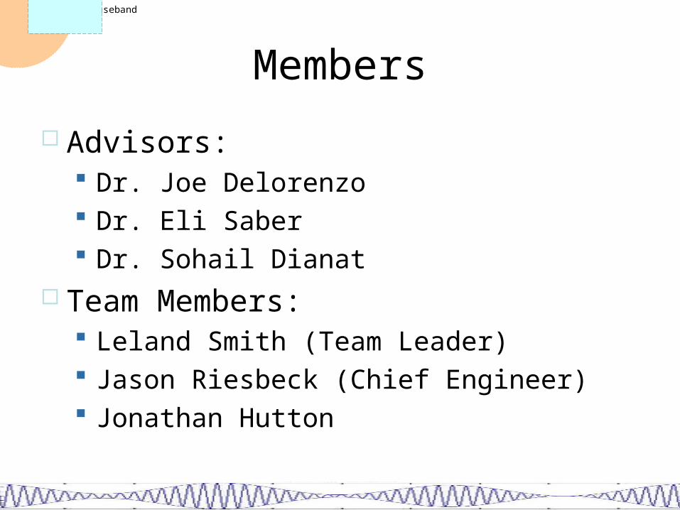
Members
Advisors: Dr. Joe Delorenzo Dr. Eli Saber Dr. Sohail Dianat
Team Members: Leland Smith (Team Leader) Jason Riesbeck (Chief Engineer) Jonathan Hutton
Communications Baseband PDR
Introduction
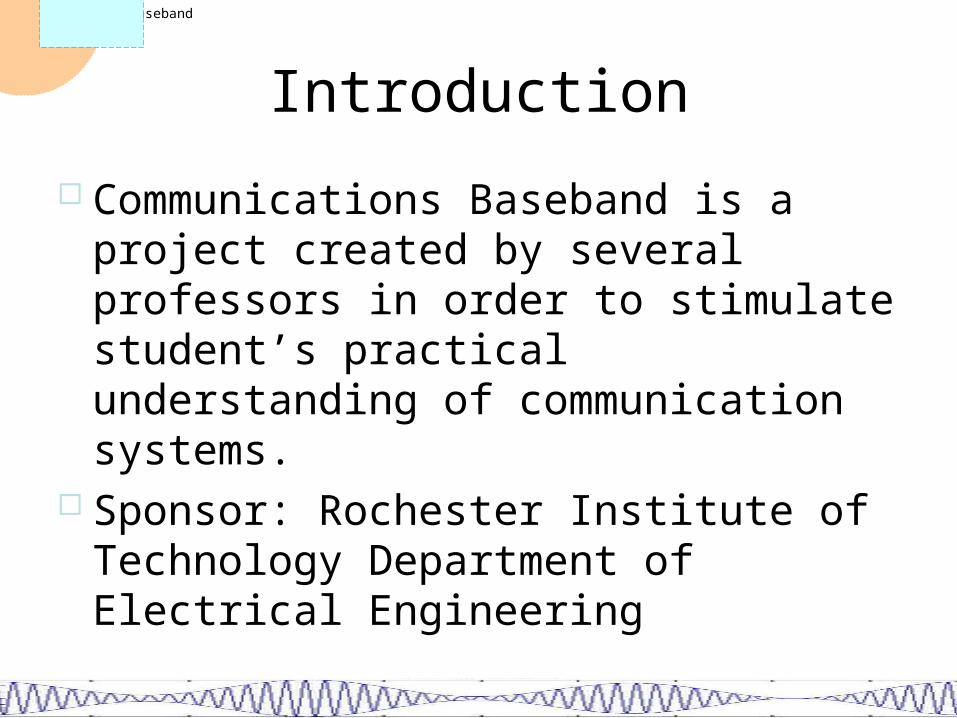
Communications Baseband is a project created by several professors in order to stimulate student’s practical understanding of communication systems.
Sponsor: Rochester Institute of Technology Department of Electrical Engineering
Communications Baseband PDR
Project Overview
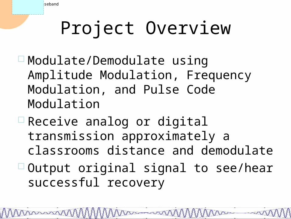
Modulate/Demodulate using Amplitude Modulation, Frequency Modulation, and Pulse Code Modulation
Receive analog or digital transmission approximately a classrooms distance and demodulate
Output original signal to see/hear successful recovery
Communications Baseband PDR
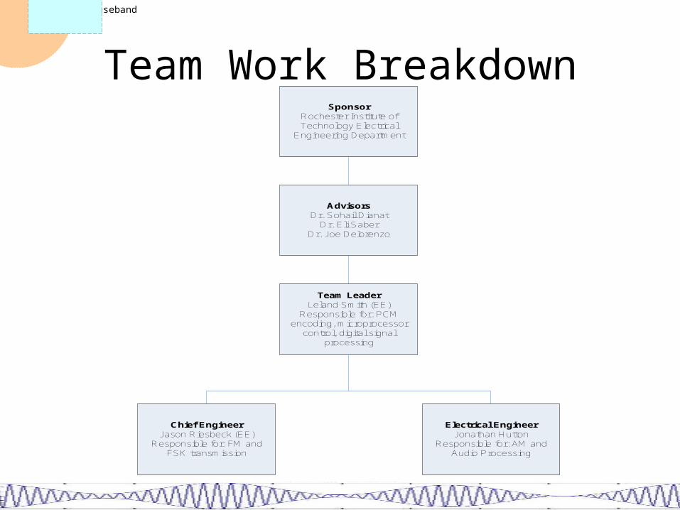
Team Work BreakdownSponsor
Rochester Institute of Technology Electrical
Engineering Department
AdvisorsDr. Sohail Dianat
Dr. Eli SaberDr. Joe Delorenzo
Team LeaderLeland Smith (EE)
Responsible for: PCM encoding, microprocessor
control, digital signal processing
Chief EngineerJason Riesbeck (EE)
Responsible for: FM and FSK transmission
Electrical EngineerJonathan Hutton
Responsible for: AM and Audio Processing
Communications Baseband PDR
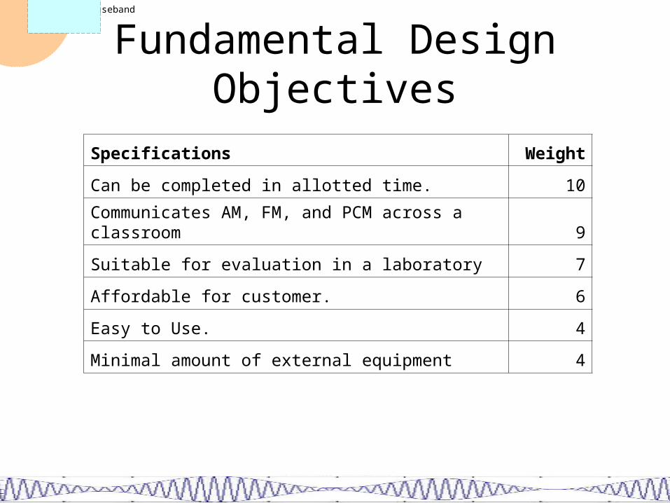
Fundamental Design Objectives
Specifications Weight
Can be completed in allotted time. 10
Communicates AM, FM, and PCM across a classroom 9
Suitable for evaluation in a laboratory 7
Affordable for customer. 6
Easy to Use. 4
Minimal amount of external equipment 4
Communications Baseband PDR
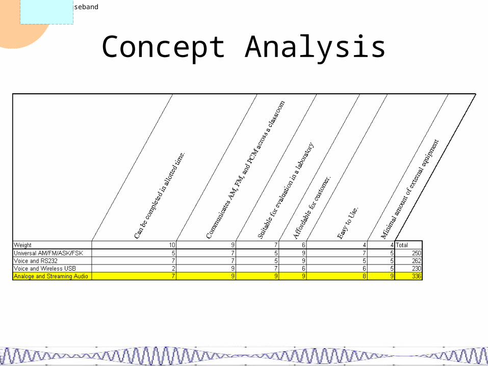
Concept Analysis
Communications Baseband PDR
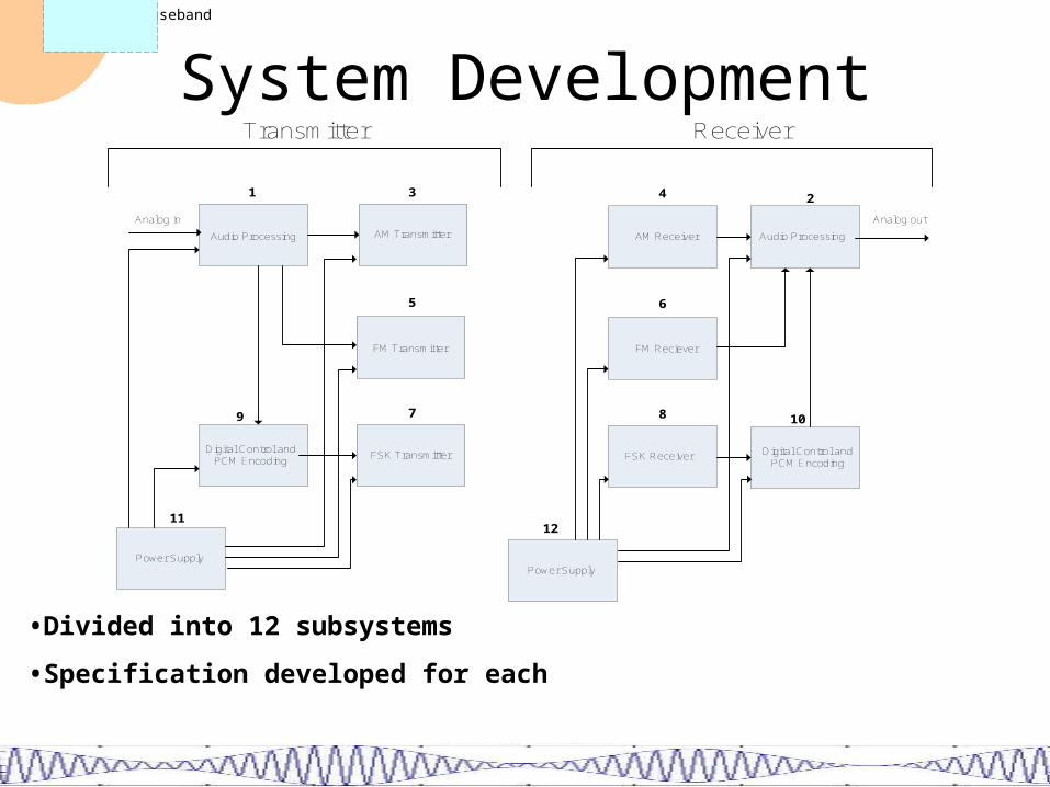
System Development
FM Transmitter
AM Transmitter
FM Reciever
AM Receiver
Analog in Analog out
FSK ReceiverFSK Transmitter Digital Control and PCM Encoding
Digital Control and PCM Encoding
Audio Processing Audio Processing
Power Supply Power Supply
1 23 4
5 6
7 89 10
1112
Transmitter Receiver
•Divided into 12 subsystems
•Specification developed for each
Communications Baseband PDR
Feasibility
Assessed at a subsystem level. Depends on the resources available
To maintain feasibility, subsystems should: Satisfy design objectives Economical Comply with time constraints
Communications Baseband PDR
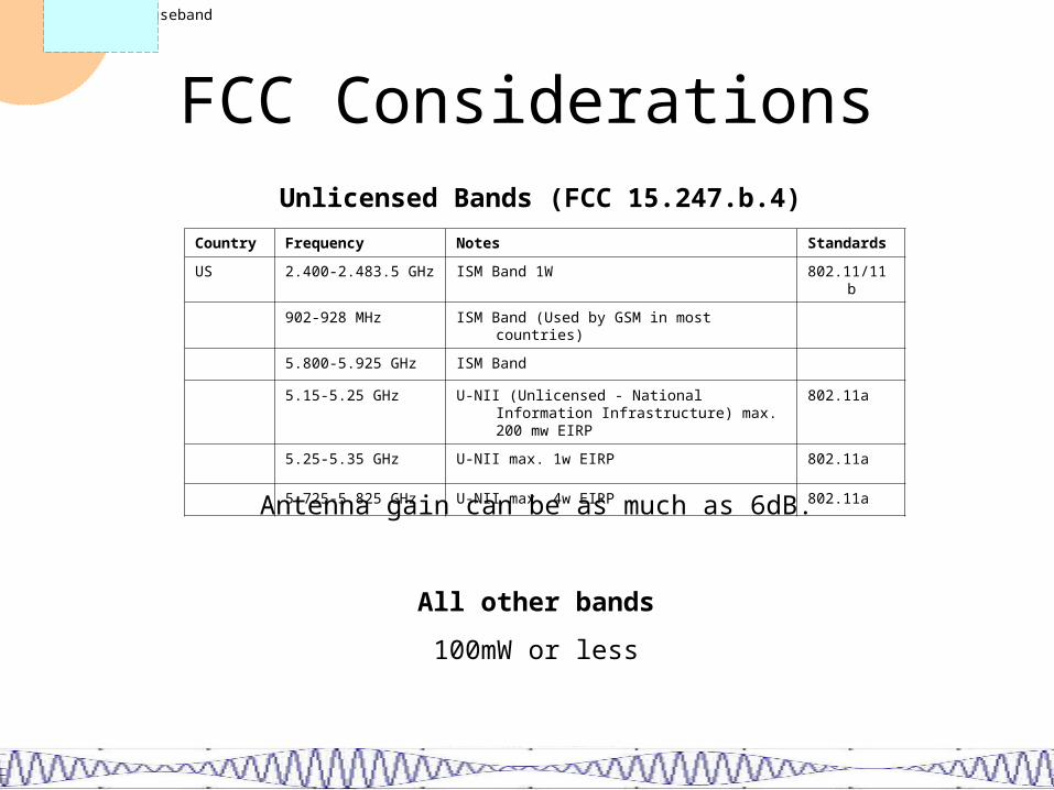
FCC Considerations
Country Frequency Notes Standards
US 2.400-2.483.5 GHz ISM Band 1W 802.11/11b
902-928 MHz ISM Band (Used by GSM in most countries)
5.800-5.925 GHz ISM Band
5.15-5.25 GHz U-NII (Unlicensed - National Information Infrastructure) max. 200 mw EIRP
802.11a
5.25-5.35 GHz U-NII max. 1w EIRP 802.11a
5.725-5.825 GHz U-NII max. 4w EIRP 802.11a
Unlicensed Bands (FCC 15.247.b.4)
All other bands
100mW or less
Antenna gain can be as much as 6dB.
Communications Baseband PDR
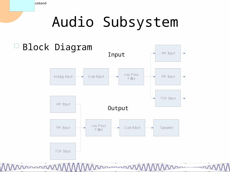
Audio Subsystem
Block Diagram
Analog Input Gain BlockLow-Pass
FilterFM Input
AM Input
FSK Input
AM Input
FM Input
FSK Input
Low-PassFilter
Gain Block Speaker
Input
Output
Communications Baseband PDR
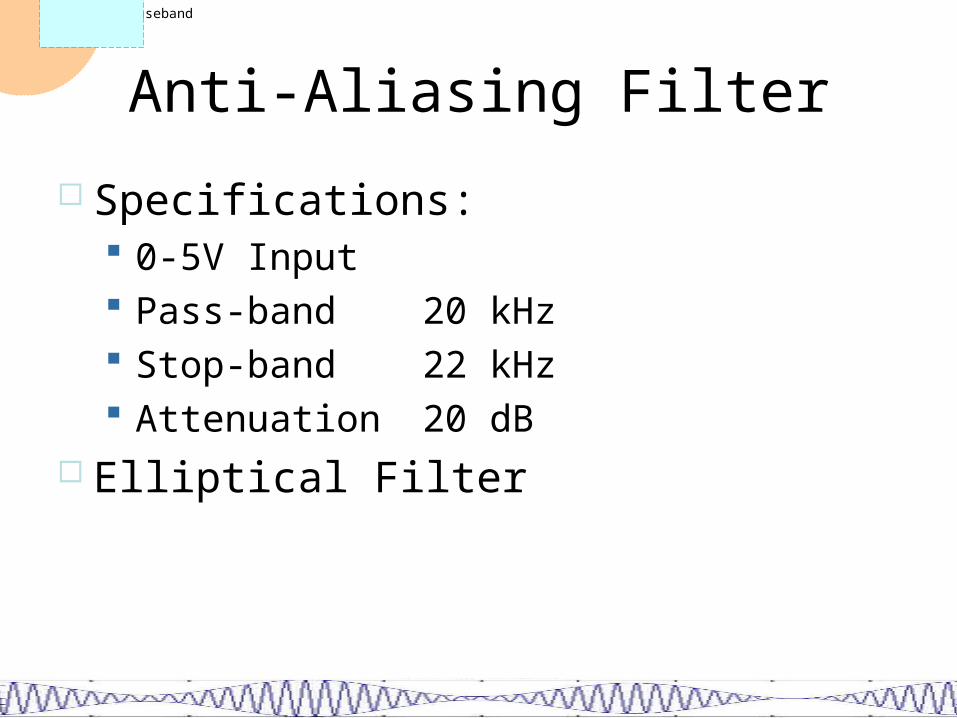
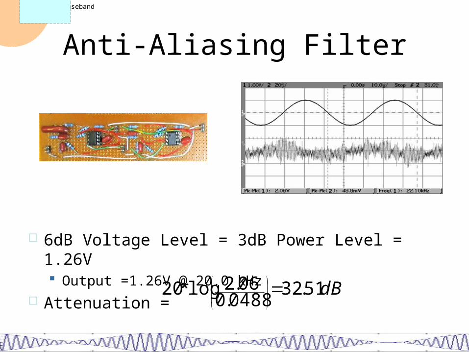
Anti-Aliasing Filter
Specifications: 0-5V Input Pass-band 20 kHz Stop-band 22 kHz Attenuation 20 dB
Elliptical Filter
Communications Baseband PDR
Anti-Aliasing FilterV
V
R 1 5
9 . 3 1 k
R 1 6
8 . 0 6 k
+3
-2
V+
7V
-4
O U T6
O S 11
O S 25
U 5
L M 7 4 1
+3
-2
V+
7V
-4
O U T6
O S 11
O S 25
U 6
L M 7 4 1
C 7
. 6 8 n
C 81 n
C 9. 3 9 n
R 1 7
1 3 0 k
R 1 8
7 . 8 7 k
R 1 9
7 . 8 7 k
R 2 0
7 . 8 7 k
R 2 13 1 6 k
R 2 21 2 1 k
V 1 00 V d c
V 1 15 V d c
0
V 1 25 V d c
V 1 30 V d c
0
0
0
+3
-2
V+
7V
-4
O U T6
O S 11
O S 25
U 7
L M 7 4 1
+3
-2
V+
7V
-4
O U T6
O S 11
O S 25
U 8
L M 7 4 1
C 1 0
7 7 7 . 5 p f
C 1 11 n
C 1 2. 2 2 n
R 2 3
1 5 . 8 k
R 2 4
9 . 0 9 k
R 2 5
9 . 0 9 k
R 2 6
9 . 0 9 k
R 2 73 5 7 k
R 2 81 5 . 0 k
V 1 40 V d c
V 1 55 V d c
V 1 65 V d c
0
V 1 70 V d c
0
0
0
0
0
V 1 82 . 5 V a c2 . 5 V d c
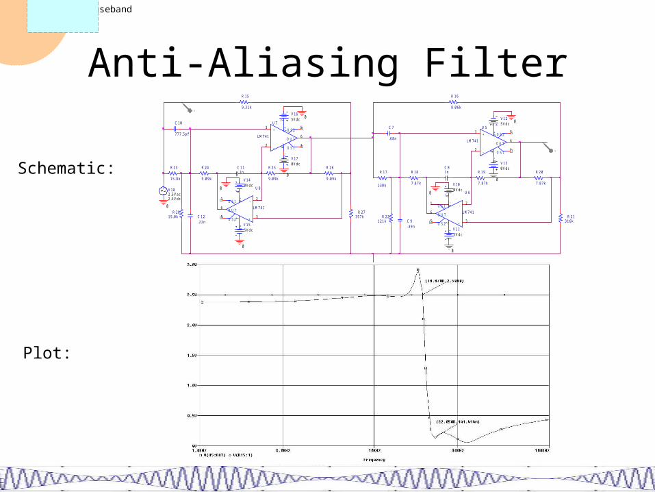
Schematic:
Plot:
Communications Baseband PDR
Anti-Aliasing Filter
6dB Voltage Level = 3dB Power Level = 1.26V Output =1.26V @ 20.0 kHz
Attenuation = dB51.320488.0
06.2log*20
Communications Baseband PDR
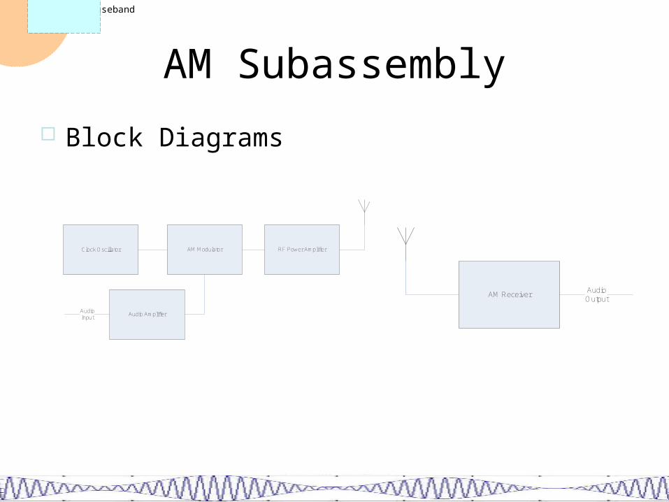
AM Subassembly
Block Diagrams
Clock Oscillator AM Modulator
Audio Amplifier
RF Power Amplifier
AudioInput
AM ReceiverAudioOutput
Communications Baseband PDR
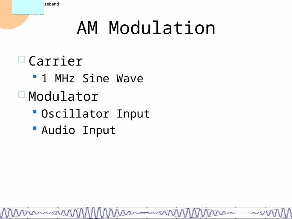
AM Modulation
Carrier 1 MHz Sine Wave
Modulator Oscillator Input Audio Input
Communications Baseband PDR
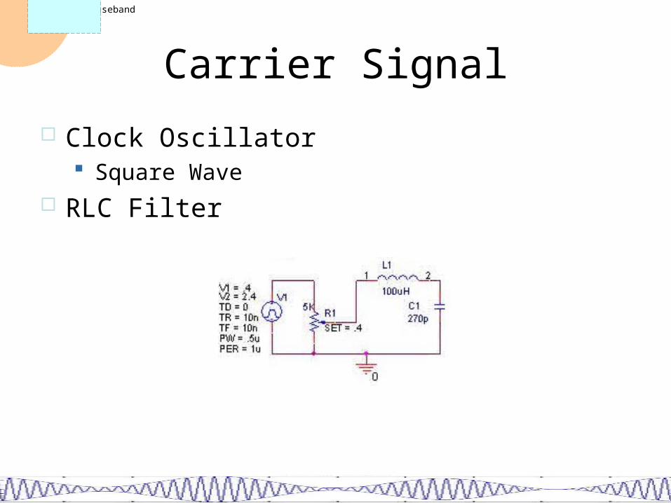
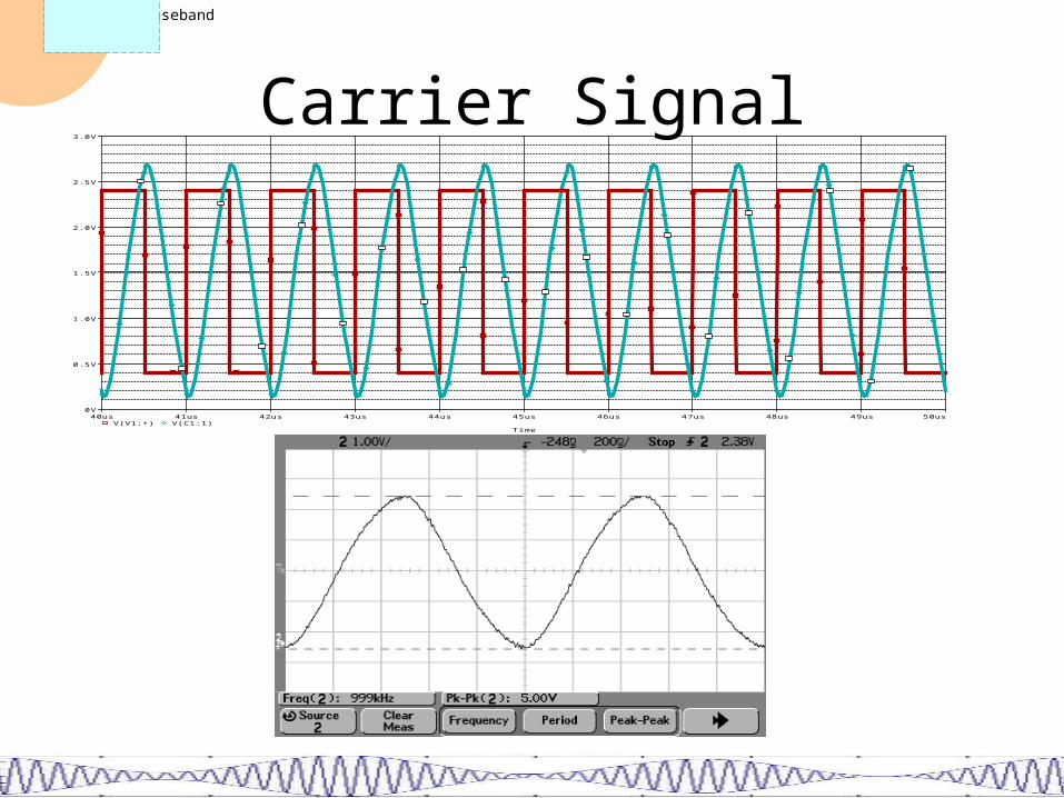
Carrier Signal
Clock Oscillator Square Wave
RLC Filter
Communications Baseband PDR
Carrier Signal
Time
40us 41us 42us 43us 44us 45us 46us 47us 48us 49us 50usV(V1:+) V(C1:1)
0V
0.5V
1.0V
1.5V
2.0V
2.5V
3.0V
Communications Baseband PDR
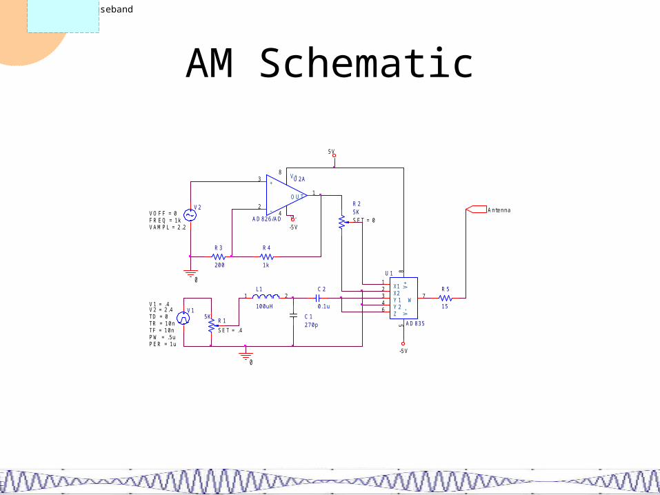
AM Schematic
V 1TD = 0
TF = 1 0 nP W = . 5 uP E R = 1 u
V 1 = . 4
TR = 1 0 n
V 2 = 2 . 4C 12 7 0 p
0
1 2L 1
1 0 0 u H
R 15 K
S E T = . 4
C 2
0 . 1 u
X11
X22
Y 13
Y 24
Z6
W7
V+
8V
-5
U 1
A D 8 3 5
+3
-2
V +8
V -4
O U T1
U 2 A
A D 8 2 6 / A D
R 25 KS E T = 0
V 2
F R E Q = 1 kV A M P L = 2 . 2
V O F F = 0
R 3
2 0 0
R 4
1 k
0
5 V
-5 V
-5 V
R 5
1 5
A n t e n n a
Communications Baseband PDR
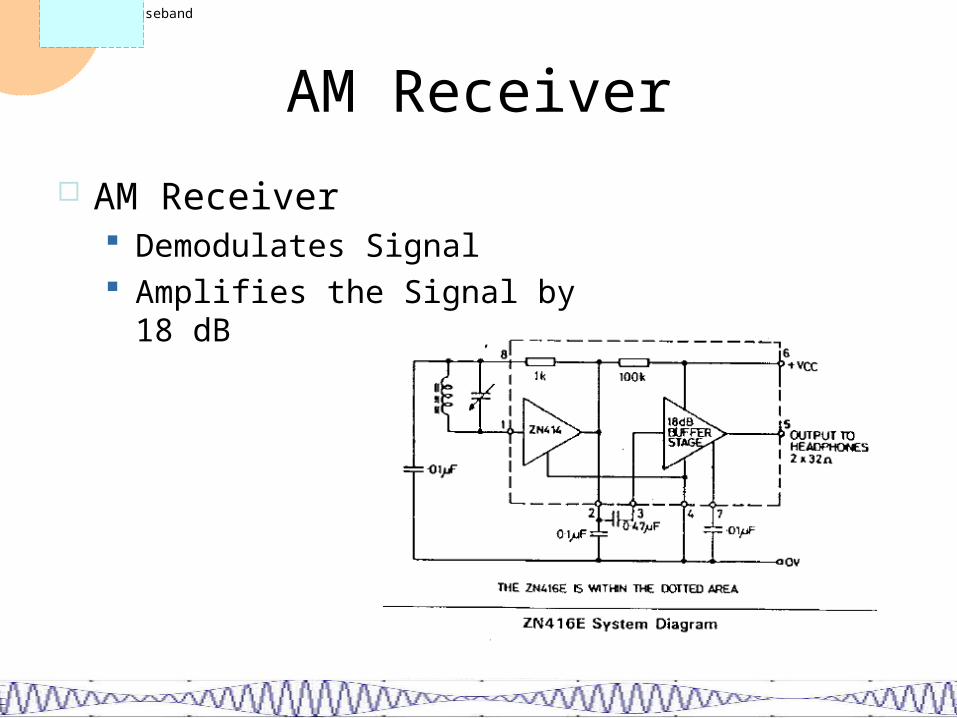
AM Receiver
AM Receiver Demodulates Signal Amplifies the Signal by 18 dB
Communications Baseband PDR
FM Systems
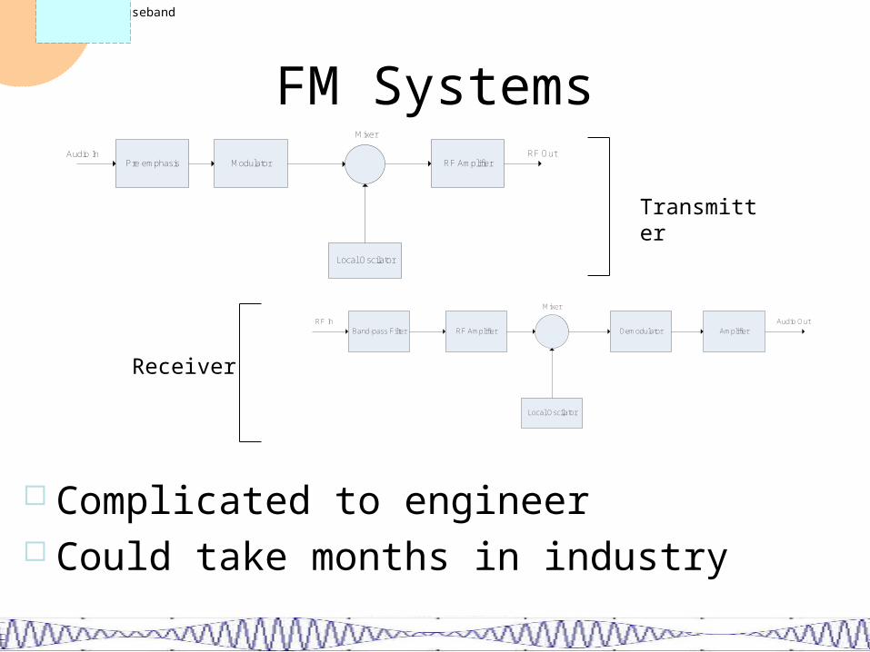
Complicated to engineer Could take months in industry
Modulator RF AmplifierPre emphasisAudio In RF Out
Local Oscilator
Mixer
Band-pass Filter RF Amplifier
Local Oscilator
Demodulator AmplifierRF In Audio Out
Mixer
Transmitter
Receiver
Communications Baseband PDR
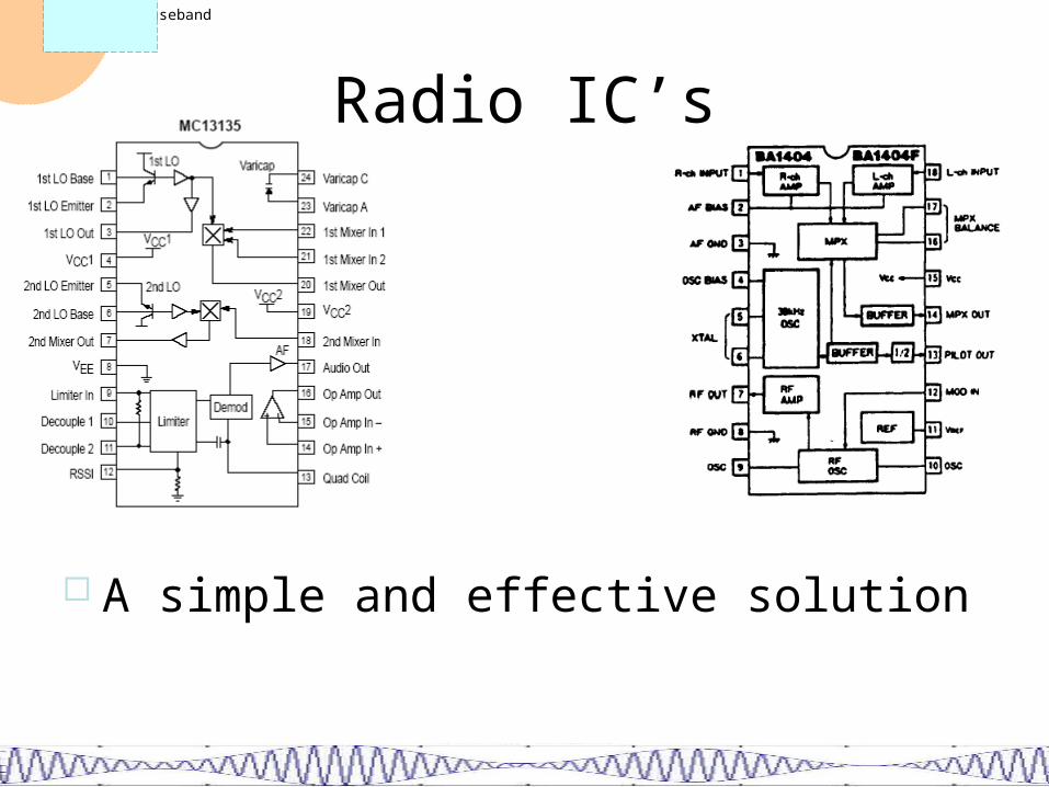
Radio IC’s
A simple and effective solution
Communications Baseband PDR
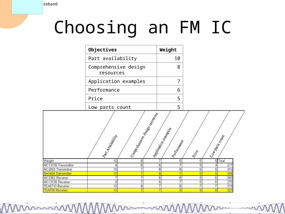
Choosing an FM ICObjectives Weight
Part availability 10
Comprehensive design resources 8
Application examples 7
Performance 6
Price 5
Low parts count 5
Communications Baseband PDR
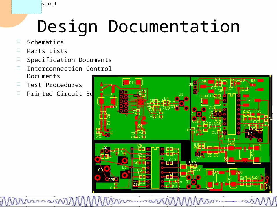
Design Documentation Schematics Parts Lists Specification Documents Interconnection Control Documents Test Procedures Printed Circuit Board
Communications Baseband PDR
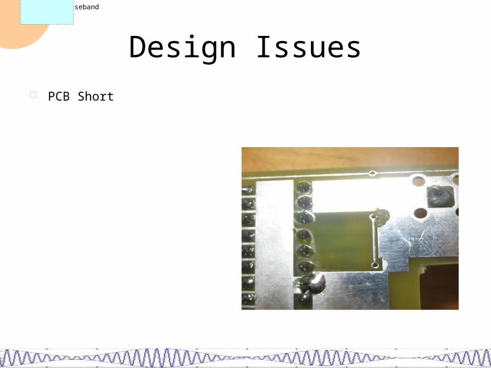
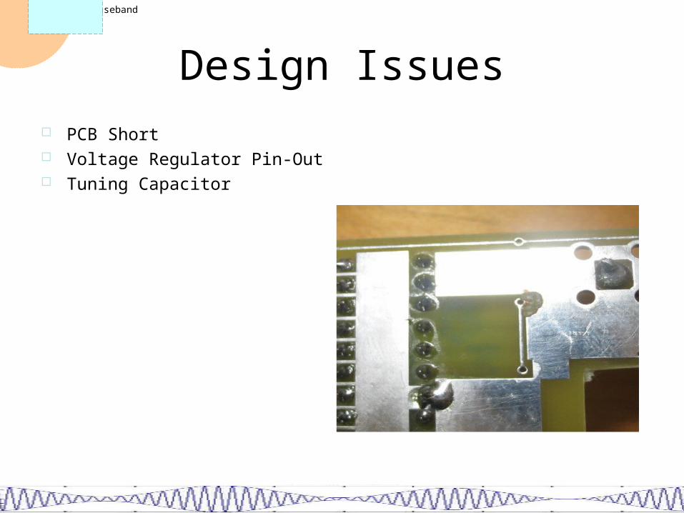
Design Issues PCB Short

Communications Baseband PDR
Design Issues PCB Short Voltage Regulator Pin-Out
Communications Baseband PDR
Design Issues PCB Short Voltage Regulator Pin-Out Tuning Capacitor
Communications Baseband PDR
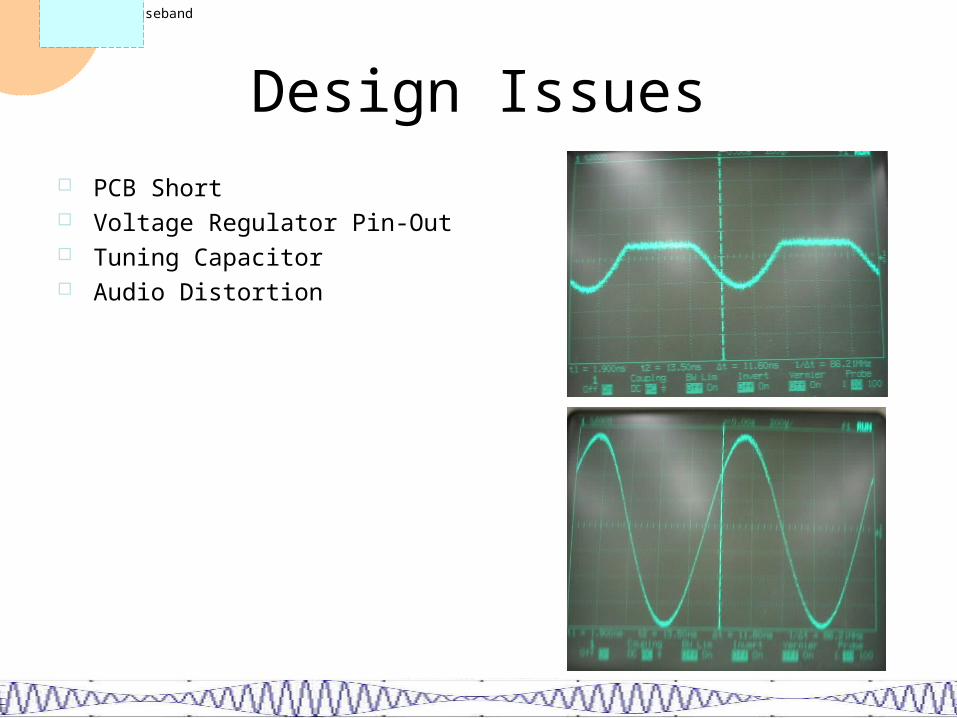
Design Issues PCB Short Voltage Regulator Pin-Out Tuning Capacitor Audio Distortion
Communications Baseband PDR
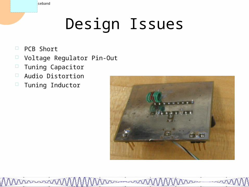
Design Issues PCB Short Voltage Regulator Pin-Out Tuning Capacitor Audio Distortion Tuning Inductor
Communications Baseband PDR
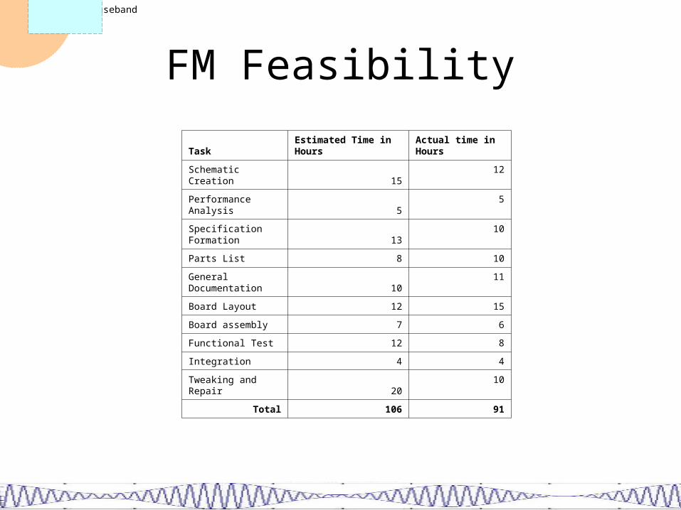
FM Feasibility
Task Estimated Time in Hours Actual time in Hours
Schematic Creation 15 12
Performance Analysis 5 5
Specification Formation 13 10
Parts List 8 10
General Documentation 10 11
Board Layout 12 15
Board assembly 7 6
Functional Test 12 8
Integration 4 4
Tweaking and Repair 20 10
Total 106 91
Communications Baseband PDR
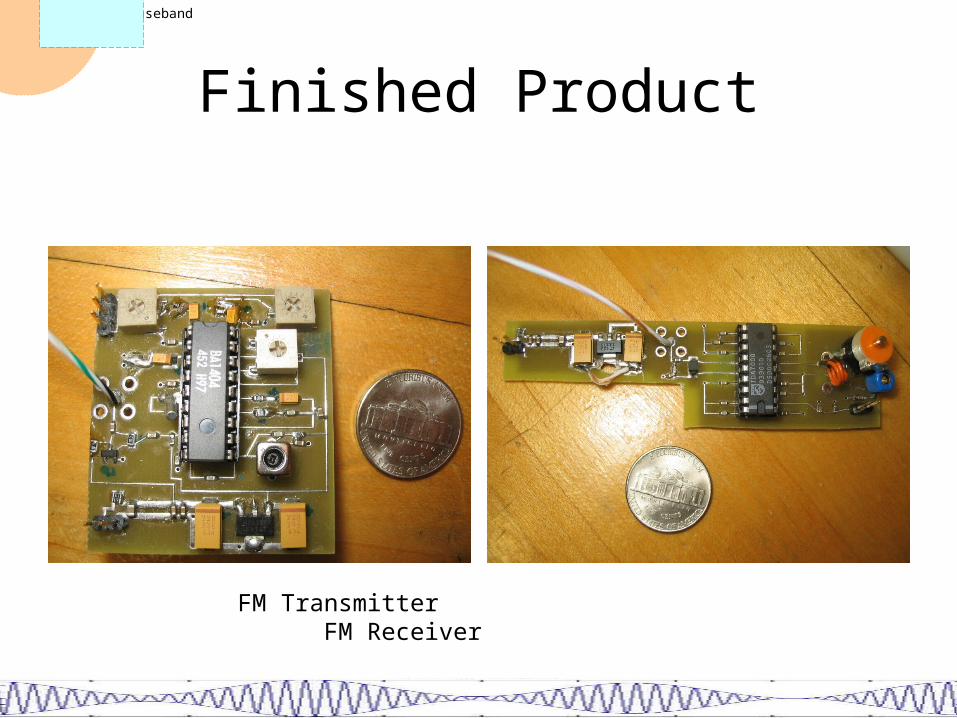
Finished Product
FM Transmitter FM Receiver
Communications Baseband PDR
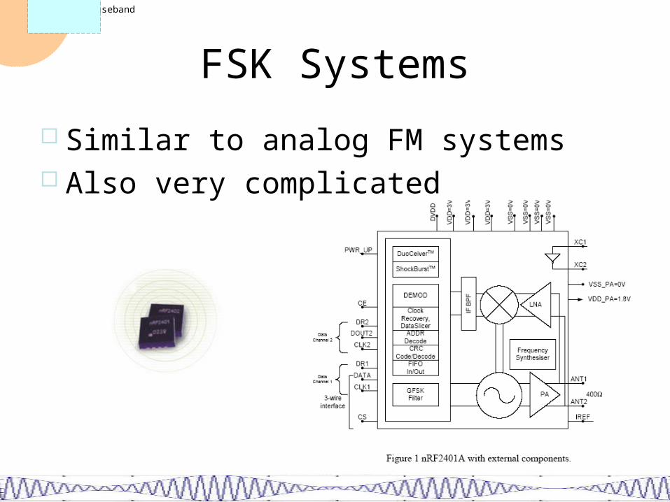
FSK Systems
Similar to analog FM systems Also very complicated
Communications Baseband PDR
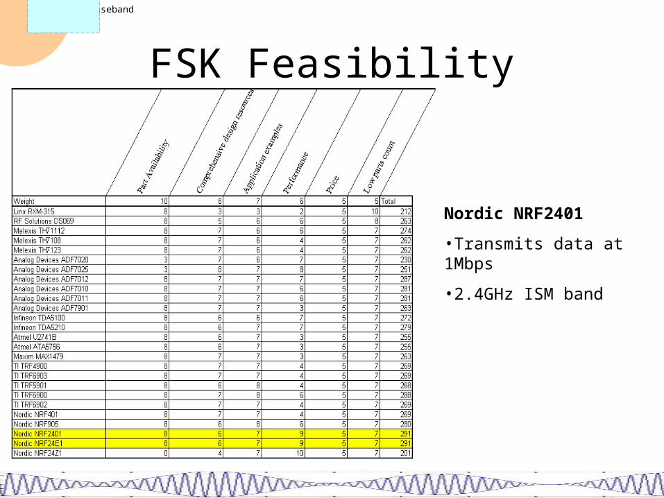
FSK Feasibility
Nordic NRF2401
•Transmits data at 1Mbps
•2.4GHz ISM band
Communications Baseband PDR
FSK Link Analysis
NRF2401 Specification○ 0dBm output power
○ -80dBm receiver sensitivity
Link Budget Analysis○ 60dB of attenuation at 10m
(with 0dB antenna gain)
Communications Baseband PDR
Design Documentation Schematics Parts Lists Specification Documents Interconnection Control
Documents Test Procedures Printed Circuit Board FSK Protocol Information
Communications Baseband PDR
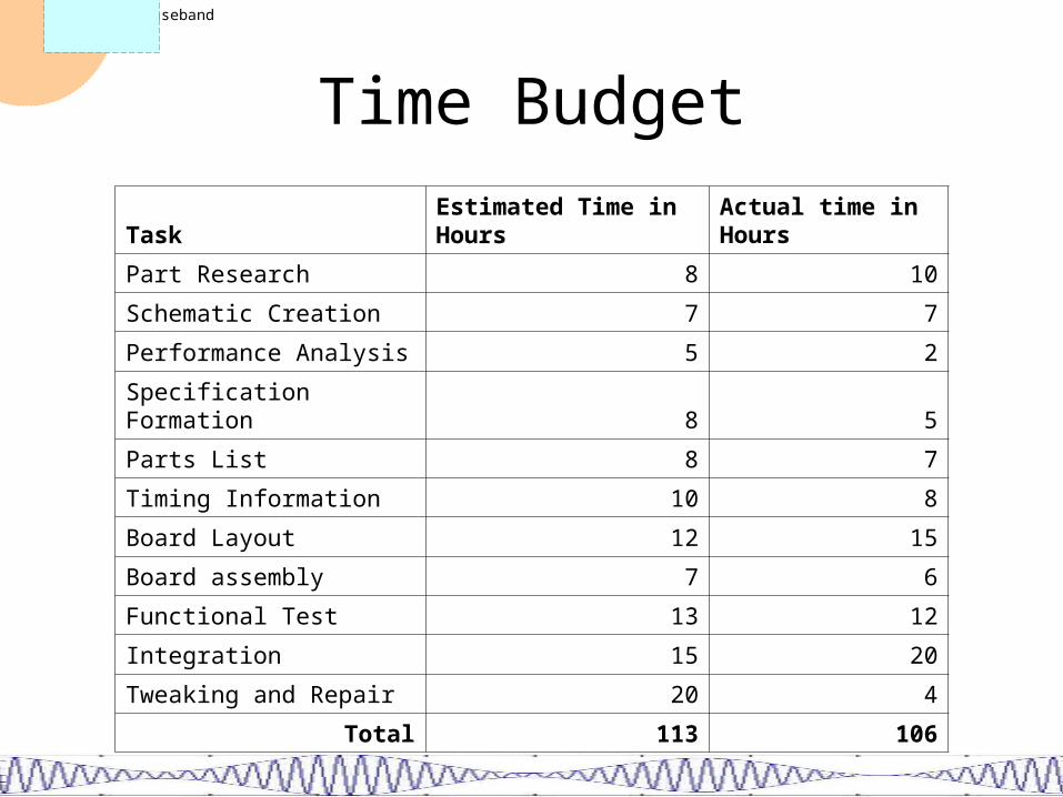
Time Budget
Task Estimated Time in Hours Actual time in Hours
Part Research 8 10
Schematic Creation 7 7
Performance Analysis 5 2
Specification Formation 8 5
Parts List 8 7
Timing Information 10 8
Board Layout 12 15
Board assembly 7 6
Functional Test 13 12
Integration 15 20
Tweaking and Repair 20 4
Total 113 106
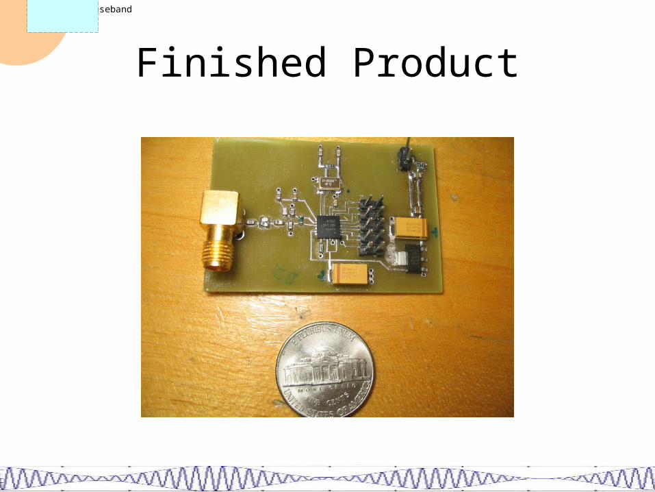
Communications Baseband PDR
Finished Product
Communications Baseband PDR
PCM and Control Subassembly
Transmit Side Conversion of Analog to Digital Apply Protocol to Digital Data Manage Memory and Data Flow to FSK Chip
Receive Side Provide Control to FSK Chip Receive and Manage FSK Chip Data Control and Send Data to DAC
Communications Baseband PDR
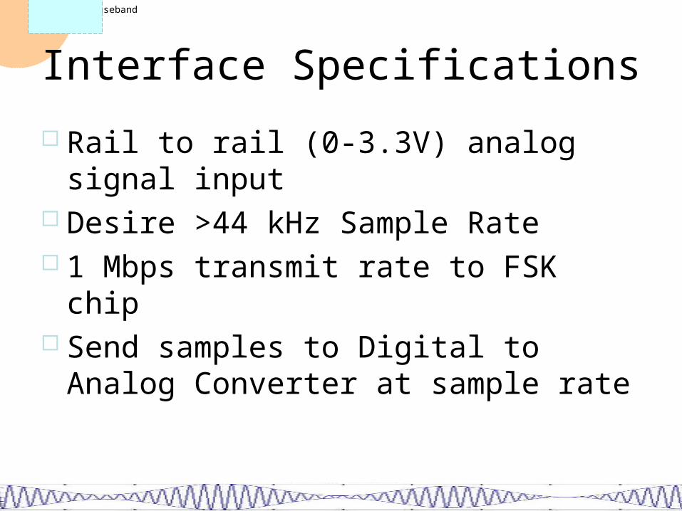
Interface Specifications
Rail to rail (0-3.3V) analog signal input Desire >44 kHz Sample Rate 1 Mbps transmit rate to FSK chip Send samples to Digital to Analog
Converter at sample rate
Communications Baseband PDR
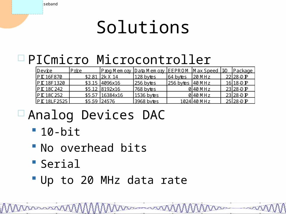
Solutions
PICmicro Microcontroller
Analog Devices DAC 10-bit No overhead bits Serial Up to 20 MHz data rate
Device Price Prog Memory Data Memory EEPROM Max Speed I/O PackagePIC16F870 $2.81 2k X 14 128 bytes 64 bytes 20 MHz 22 28-DIPPIC18F1320 $3.15 4096x16 256 bytes 256 bytes 40 MHz 16 18-DIPPIC18C242 $5.12 8192x16 768 bytes 0 40 MHz 23 28-DIPPIC18C252 $5.57 16384x16 1536 bytes 0 40 MHz 23 28-DIPPIC18LF2525 $5.59 24576 3968 bytes 1024 40 MHz 25 28-DIP
Communications Baseband PDR
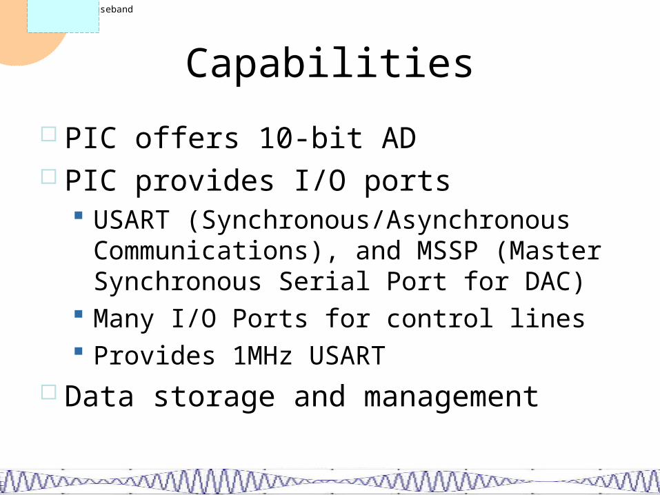
Capabilities
PIC offers 10-bit AD PIC provides I/O ports
USART (Synchronous/Asynchronous Communications), and MSSP (Master Synchronous Serial Port for DAC)
Many I/O Ports for control lines Provides 1MHz USART
Data storage and management
Communications Baseband PDR
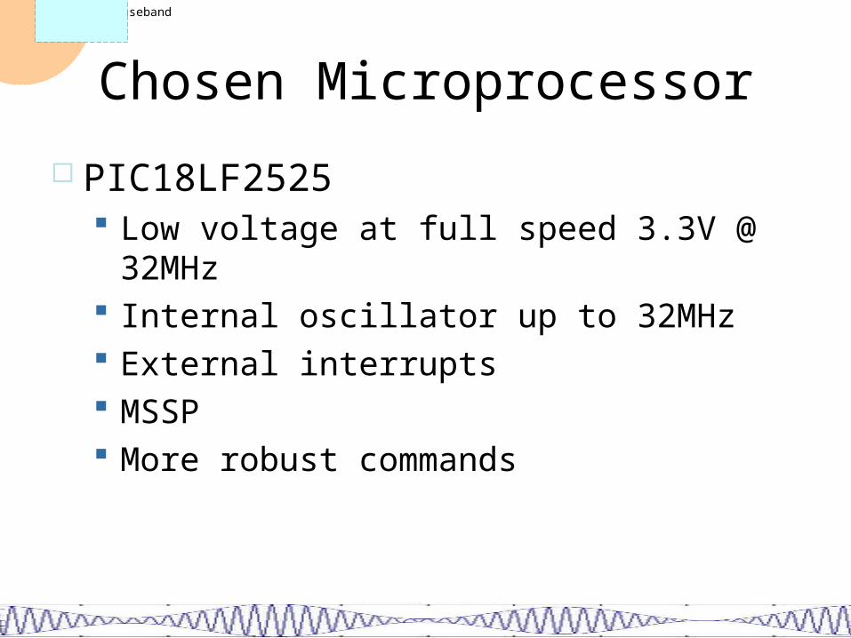
Chosen Microprocessor
PIC18LF2525 Low voltage at full speed 3.3V @ 32MHz Internal oscillator up to 32MHz External interrupts MSSP More robust commands
Communications Baseband PDR
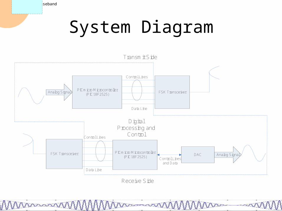
System Diagram
PICmicro Microcontroller(PIC18F2525)
Analog Signal FSK Transceiver
Transmit Side
Receive Side
Control Lines
Data Line
PICmicro Microcontroller(PIC18F2525)
FSK Transceiver
Control Lines
Data Line
DACControl Lines
and Data
Analog Signal
Digital Processing and
Control
Communications Baseband PDR
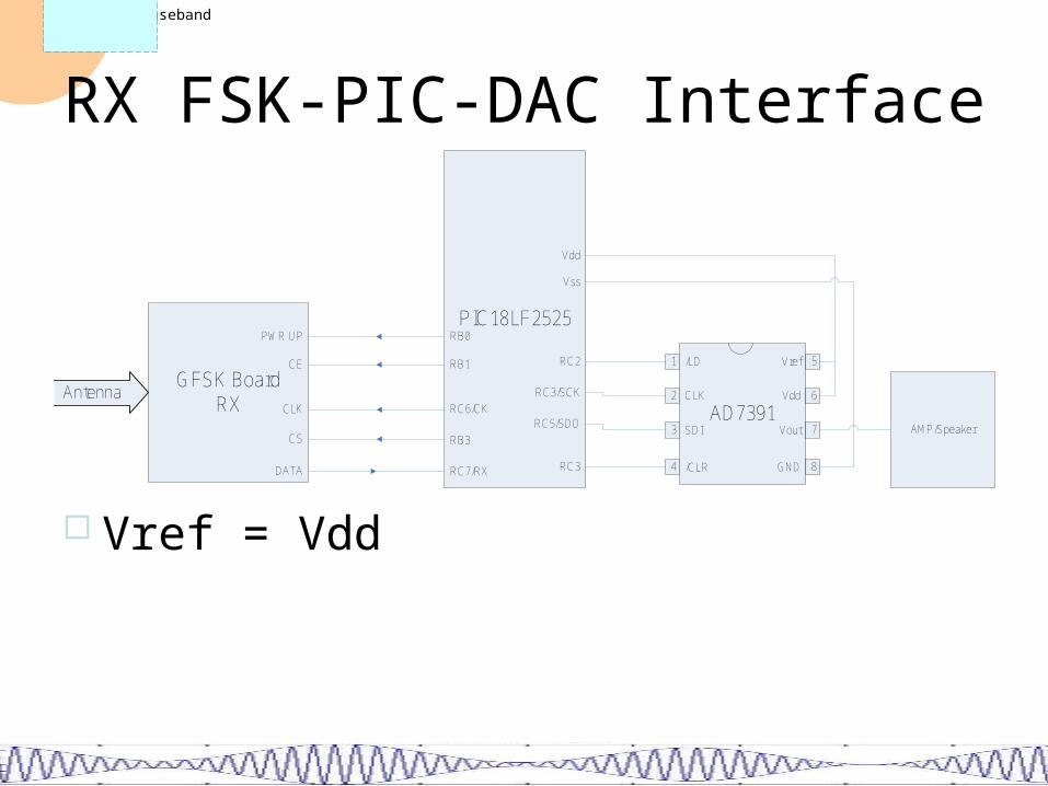
RX FSK-PIC-DAC Interface
PIC18LF2525
GFSK BoardRX
RC7/RXDATA
PWR UP RB0
RB1CE
RC6/CKCLK
RB3CS
AntennaAD7391
Vref 5
6
7
8
1
2
3
4
Vdd
Vout
GND
/LD
CLK
SDI
/CLR
RC3/SCK
RC2
RC5/SDO
Vdd
Vss
RC3
AMP/Speaker
Vref = Vdd
Communications Baseband PDR
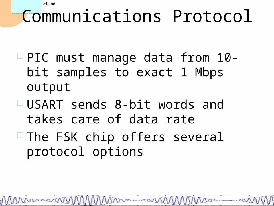
Communications Protocol
PIC must manage data from 10-bit samples to exact 1 Mbps output
USART sends 8-bit words and takes care of data rate
The FSK chip offers several protocol options
Communications Baseband PDR
IN PIC OUT
Known: What goes in must come out – and at the same rate.
Therefore: The rate the PIC can sample at is governed by the FSK communications protocol.
Sampling rate must be some integer number of the outgoing packet rate
Communications Baseband PDR
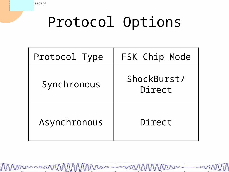
Protocol Options
Protocol Type FSK Chip Mode
Synchronous ShockBurst/Direct
Asynchronous Direct
Communications Baseband PDR
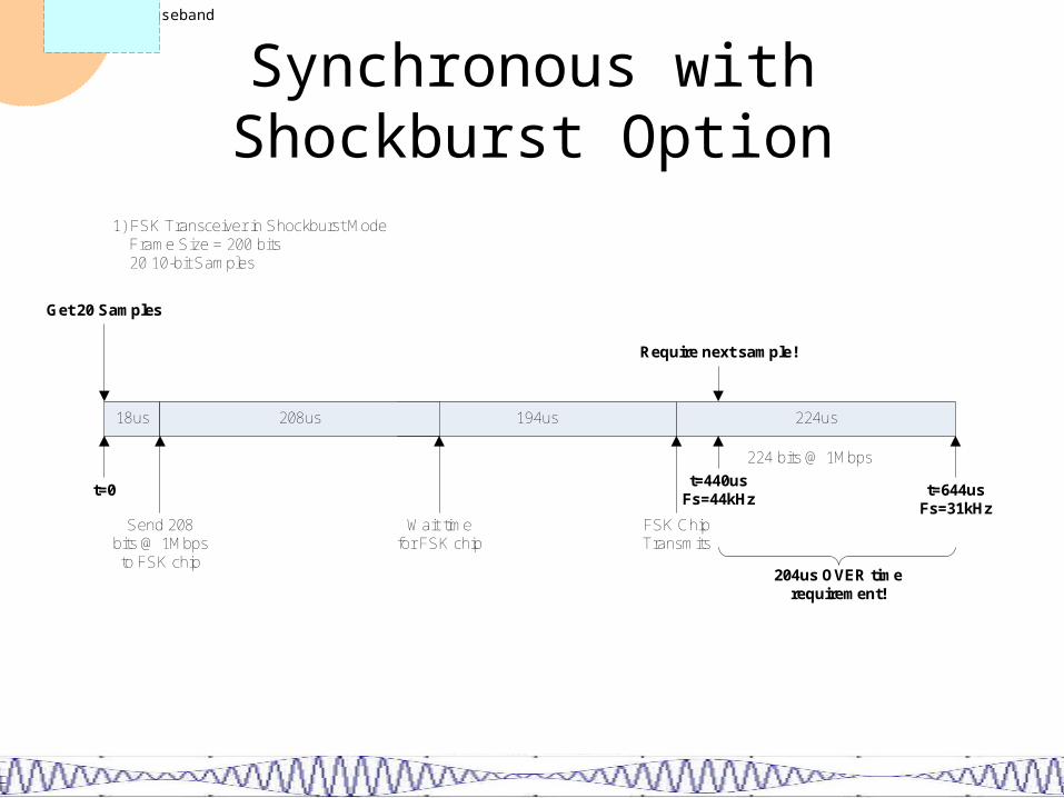
Synchronous with Shockburst Option
18us
Get 20 Samples
t=0
194us
224 bits @ 1Mbps
Require next sample!
t=440usFs=44kHz
1) FSK Transceiver in Shockburst Mode Frame Size = 200 bits 20 10-bit Samples
208us
Send 208 bits @ 1Mbpsto FSK chip
Wait timefor FSK chip
FSK Chip Transmits
224us
204us OVER time requirement!
t=644usFs=31kHz
Communications Baseband PDR
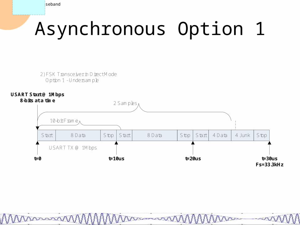
Asynchronous Option 1
2) FSK Transceiver in Direct Mode Option 1 - Undersample
Start
USART Start @ 1Mbps8-bits at a time
t=0
Stop8 Data Start Stop8 Data Start Stop4 Data
t=10us
USART TX @ 1Mbps
10-bit Frame
t=20us t=30usFs=33.3kHz
2 Samples
4 Junk
Communications Baseband PDR
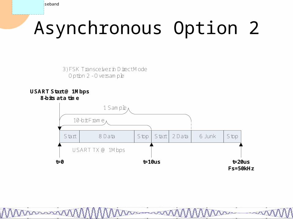
Asynchronous Option 2
3) FSK Transceiver in Direct Mode Option 2 - Oversample
Start
USART Start @ 1Mbps8-bits at a time
t=0
Stop8 Data Start Stop2 Data
t=10us
USART TX @ 1Mbps
10-bit Frame
t=20usFs=50kHz
1 Sample
6 Junk
Communications Baseband PDR
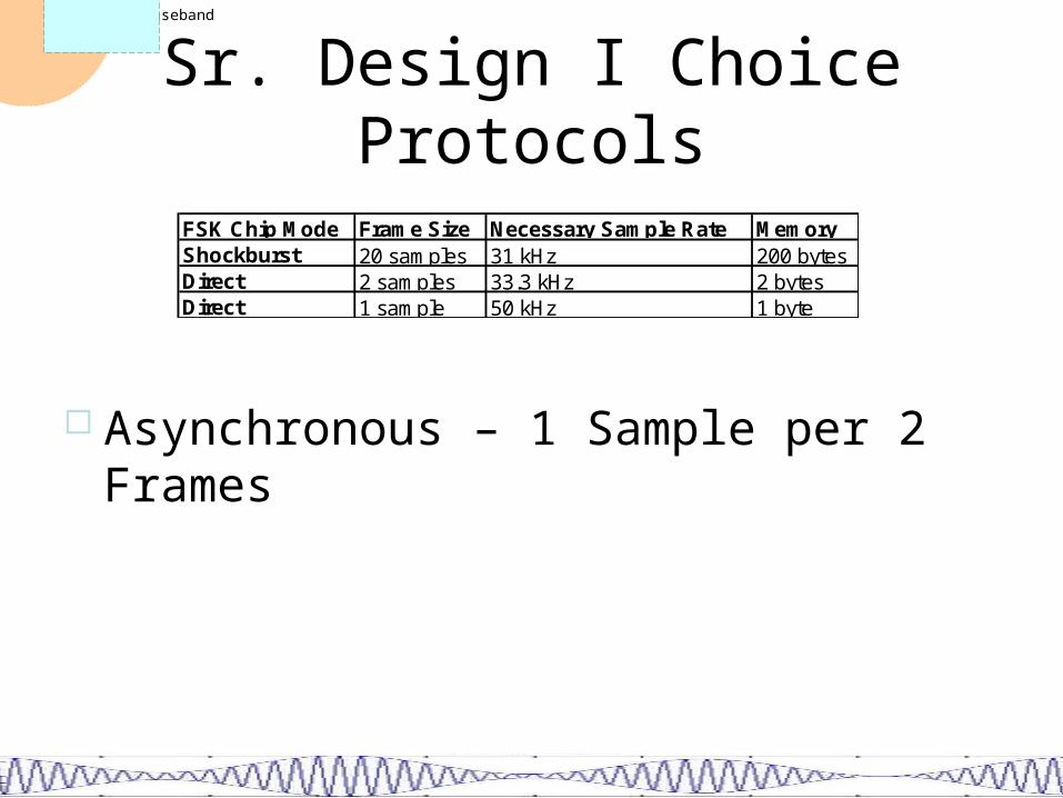
Sr. Design I Choice Protocols
Asynchronous – 1 Sample per 2 Frames
FSK Chip Mode Frame Size Necessary Sample Rate Memory Shockburst 20 samples 31 kHz 200 bytesDirect 2 samples 33.3 kHz 2 bytesDirect 1 sample 50 kHz 1 byte
Communications Baseband PDR
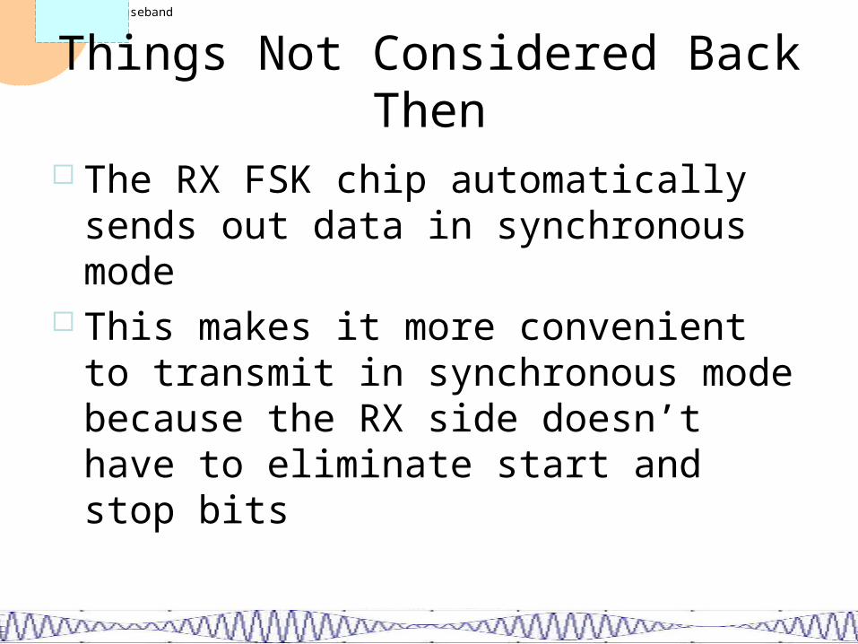
Things Not Considered Back Then
The RX FSK chip automatically sends out data in synchronous mode
This makes it more convenient to transmit in synchronous mode because the RX side doesn’t have to eliminate start and stop bits
Communications Baseband PDR
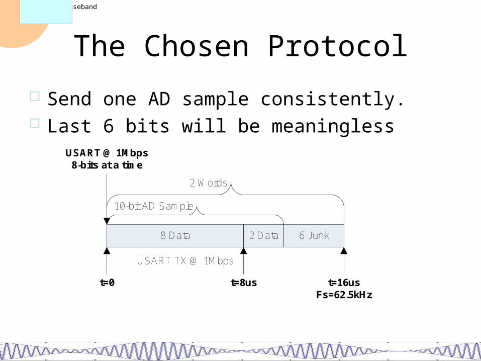
The Chosen Protocol
Send one AD sample consistently. Last 6 bits will be meaningless
USART @ 1Mbps8-bits at a time
t=0
8 Data 2 Data
t=8us
USART TX @ 1Mbps
10-bit AD Sample
t=16usFs=62.5kHz
2 Words
6 Junk
Communications Baseband PDR
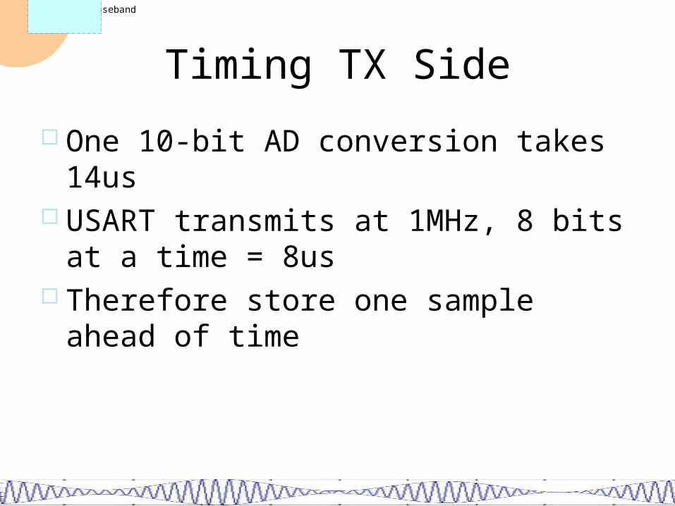
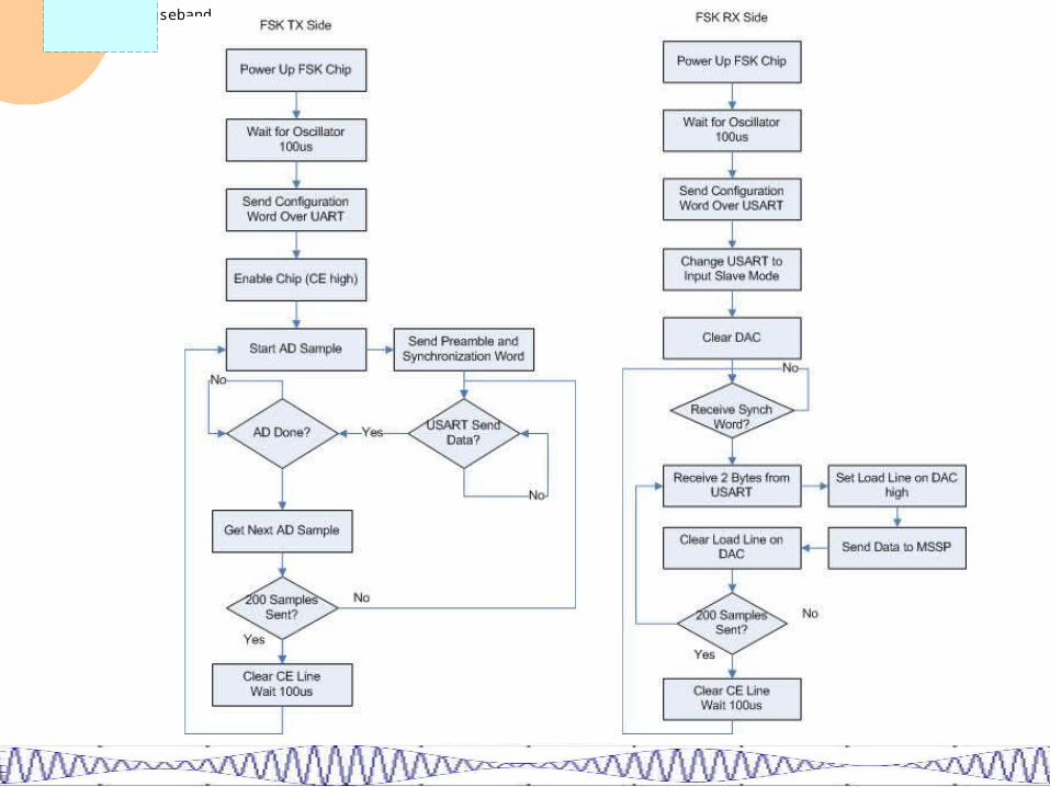
Timing TX Side
One 10-bit AD conversion takes 14us USART transmits at 1MHz, 8 bits at a time
= 8us Therefore store one sample ahead of time
Communications Baseband PDR
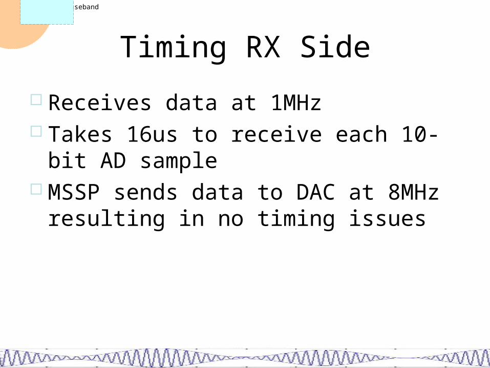
Timing RX Side
Receives data at 1MHz Takes 16us to receive each 10-bit AD
sample MSSP sends data to DAC at 8MHz
resulting in no timing issues
Communications Baseband PDR
Communications Baseband PDR
FSK Chip Requirements
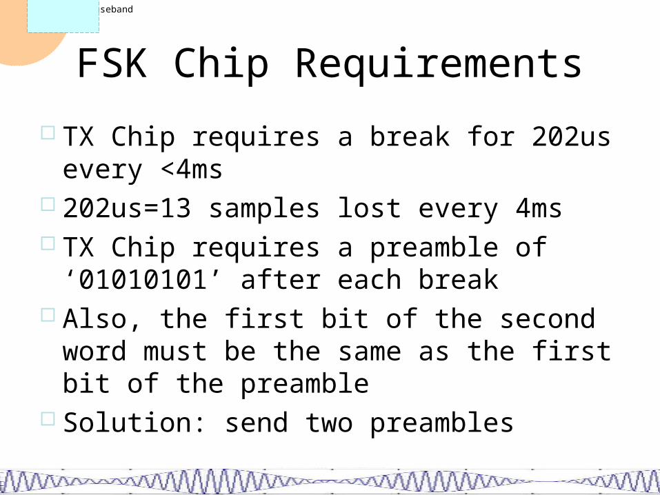
TX Chip requires a break for 202us every <4ms
202us=13 samples lost every 4ms TX Chip requires a preamble of
‘01010101’ after each break Also, the first bit of the second word must
be the same as the first bit of the preamble Solution: send two preambles
Communications Baseband PDR
Design Issues
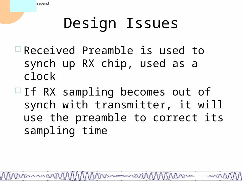
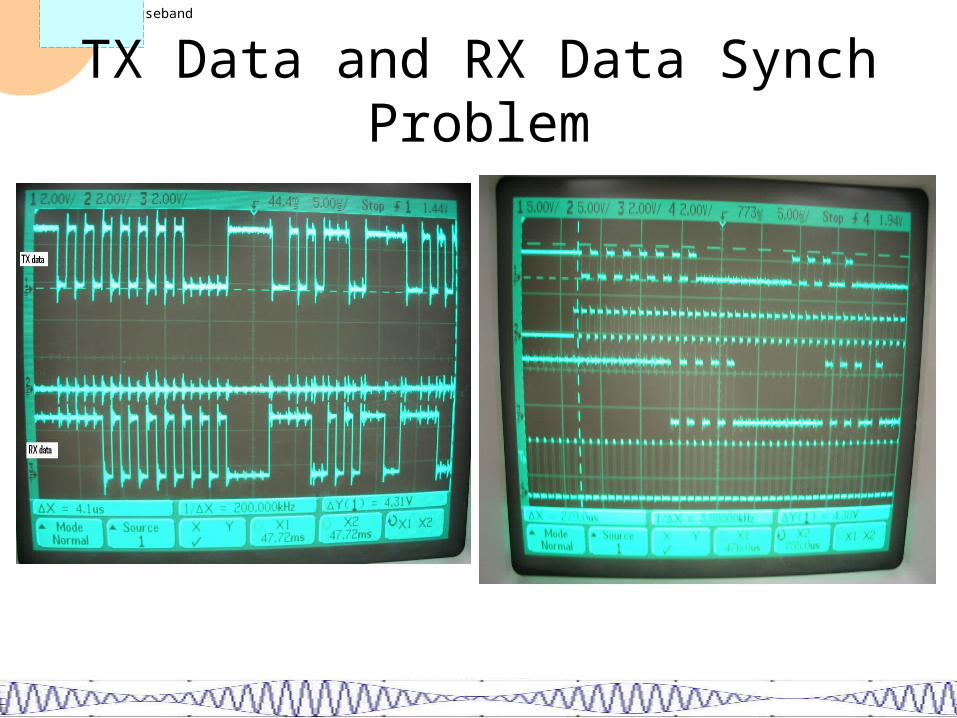
Received Preamble is used to synch up RX chip, used as a clock
If RX sampling becomes out of synch with transmitter, it will use the preamble to correct its sampling time
Communications Baseband PDR
TX Data and RX Data Synch Problem
Communications Baseband PDR
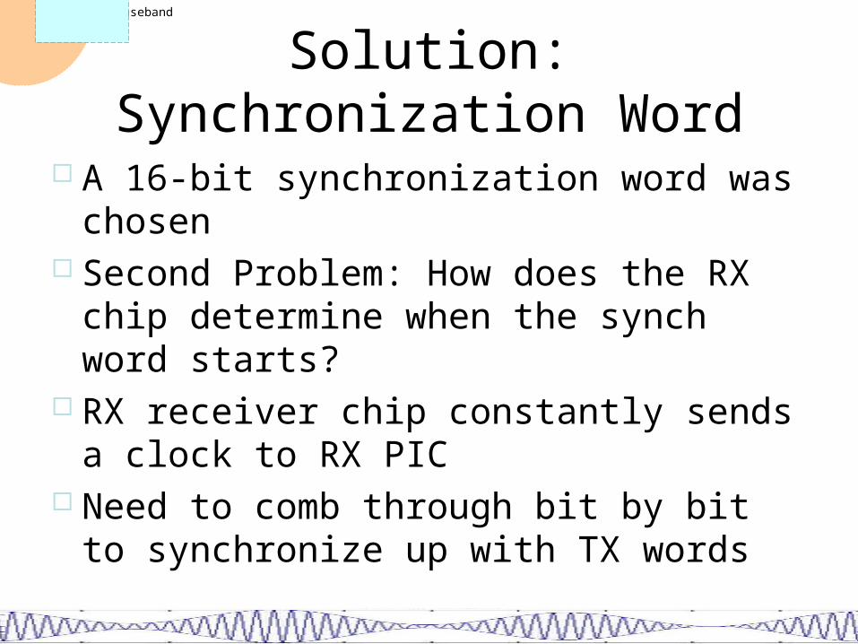
Solution: Synchronization Word
A 16-bit synchronization word was chosen Second Problem: How does the RX chip
determine when the synch word starts? RX receiver chip constantly sends a clock
to RX PIC Need to comb through bit by bit to
synchronize up with TX words
Communications Baseband PDR
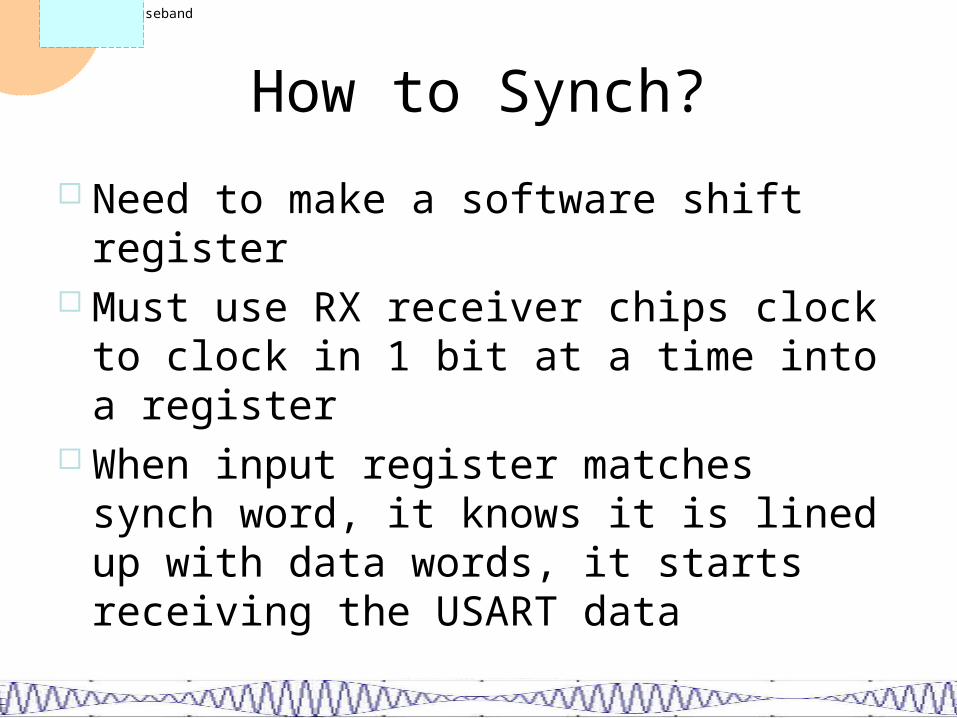
How to Synch?
Need to make a software shift register Must use RX receiver chips clock to clock
in 1 bit at a time into a register When input register matches synch word,
it knows it is lined up with data words, it starts receiving the USART data
Communications Baseband PDR
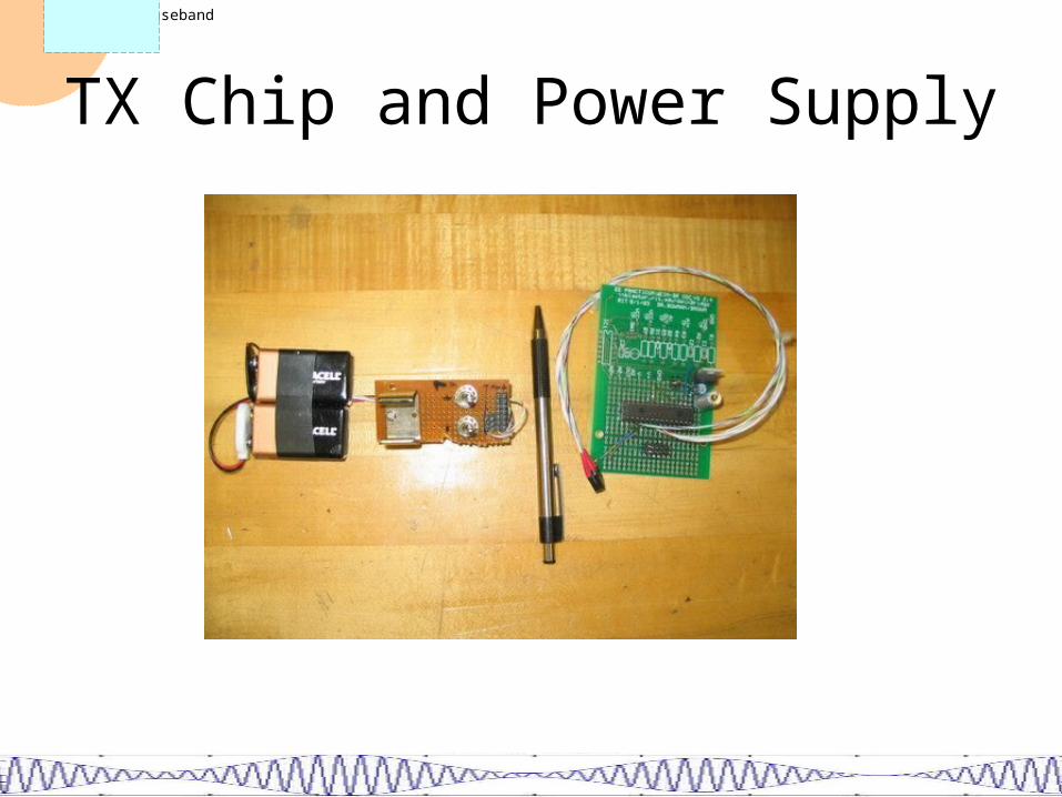
TX Chip and Power Supply
Communications Baseband PDR
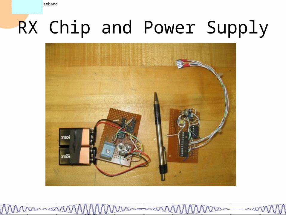
RX Chip and Power Supply
Communications Baseband PDR
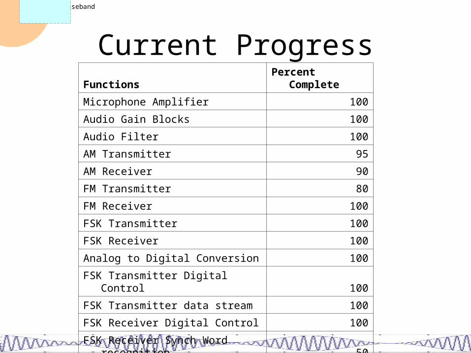
Current ProgressFunctions Percent Complete
Microphone Amplifier 100
Audio Gain Blocks 100
Audio Filter 100
AM Transmitter 95
AM Receiver 90
FM Transmitter 80
FM Receiver 100
FSK Transmitter 100
FSK Receiver 100
Analog to Digital Conversion 100
FSK Transmitter Digital Control 100
FSK Transmitter data stream 100
FSK Receiver Digital Control 100
FSK Receiver Synch Word recognition 50
Communications Baseband PDR
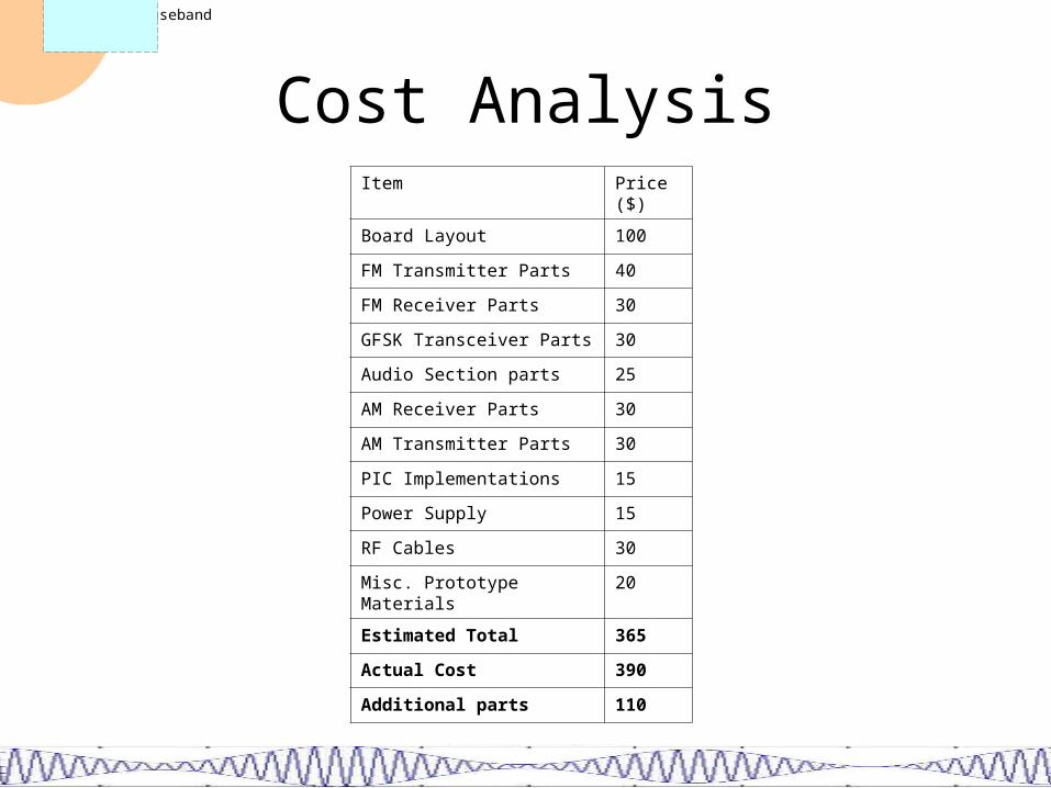
Cost AnalysisItem Price ($)
Board Layout 100
FM Transmitter Parts 40
FM Receiver Parts 30
GFSK Transceiver Parts 30
Audio Section parts 25
AM Receiver Parts 30
AM Transmitter Parts 30
PIC Implementations 15
Power Supply 15
RF Cables 30
Misc. Prototype Materials 20
Estimated Total 365
Actual Cost 390
Additional parts 110
Communications Baseband PDR
Future Improvements / Spin-offs
Improve Quality of FM Transmitter Refine code to make digital transmission
more robust (i.e. data encoding, error detection).
Organize systems into student projects, labs, or class curriculums.
Add digital serial transmission using MSSP

Communications Baseband PDR
Questions?