Embed Size (px)
Citation preview
© COPYRIGHT 2013, COMSOL, Inc, Keynote at 9th Workshop on Numerical Methods for Optical Nano Structures, ETH Zurich, Jul 1, 2013
Novelties in COMSOL for Modeling Optical Nanostructures
Sven FriedelCOMSOL Multiphysics GmbH, Zürich
Chemical Reactions Acoustics
Electrodynamics Heat Transfer
Fluid DynamicsMechanics
User Defined PDE
Multiphysics
COMSOL – an integrated simulation environment
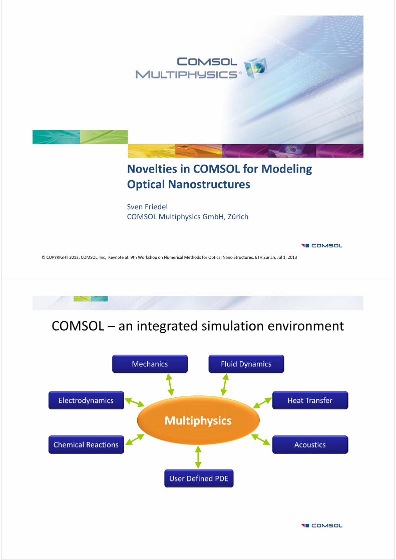
Electrodynamics
Biochemistry Photon‐Phonon
Photo‐Thermal
Opto‐FluidicsOpto‐Mechanics
Non‐local, QM effects
Optical Nanostructures ‐Multiphysics Systems?
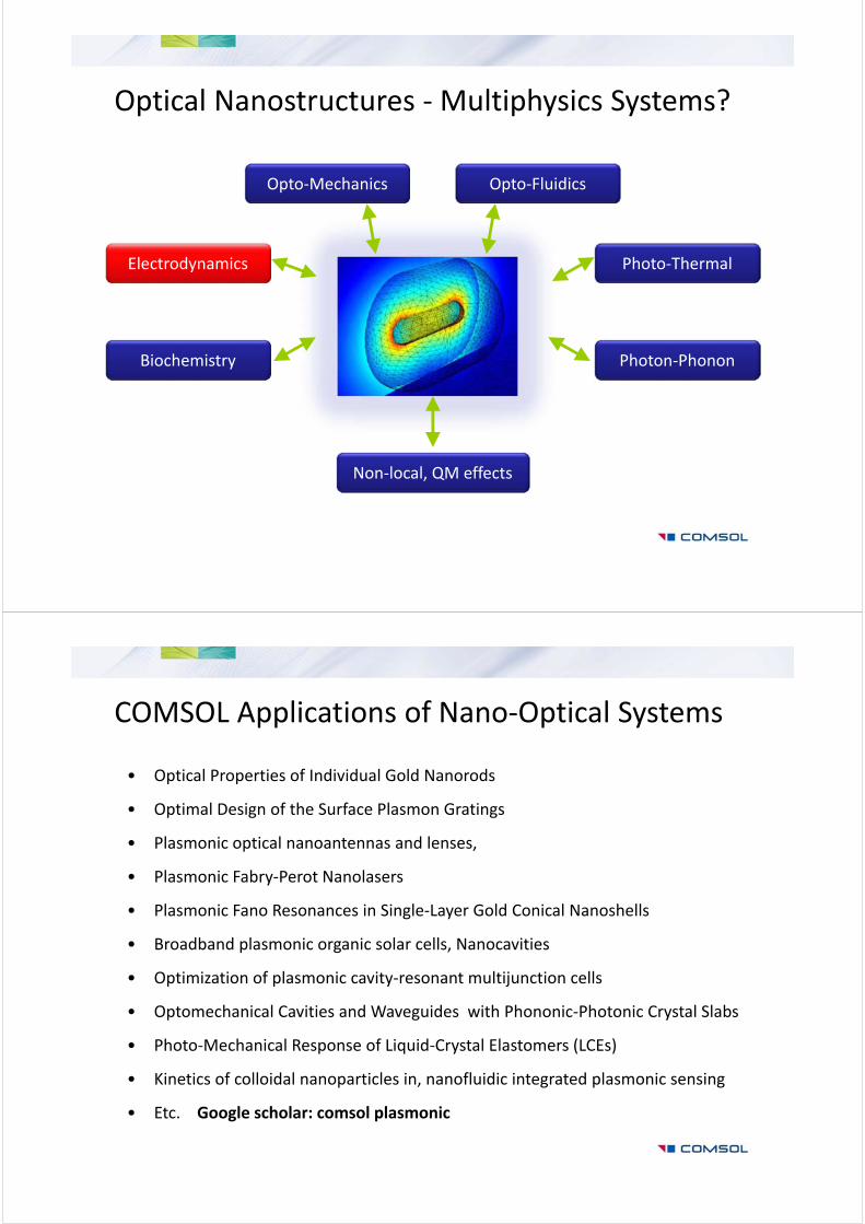
• Optical Properties of Individual Gold Nanorods
• Optimal Design of the Surface Plasmon Gratings
• Plasmonic optical nanoantennas and lenses,
• Plasmonic Fabry‐Perot Nanolasers
• Plasmonic Fano Resonances in Single‐Layer Gold Conical Nanoshells
• Broadband plasmonic organic solar cells, Nanocavities
• Optimization of plasmonic cavity‐resonant multijunction cells
• Optomechanical Cavities and Waveguides with Phononic‐Photonic Crystal Slabs
• Photo‐Mechanical Response of Liquid‐Crystal Elastomers (LCEs)
• Kinetics of colloidal nanoparticles in, nanofluidic integrated plasmonic sensing
• Etc. Google scholar: comsol plasmonic
COMSOL Applications of Nano‐Optical Systems
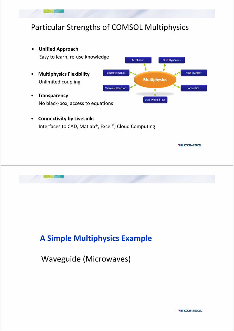
• Multiphysics Flexibility
Unlimited coupling
• Unified Approach
Easy to learn, re‐use knowledge
• Transparency
No black‐box, access to equations
• Connectivity by LiveLinks
Interfaces to CAD, Matlab®, Excel®, Cloud Computing
Particular Strengths of COMSOL Multiphysics
Waveguide (Microwaves)
A Simple Multiphysics Example
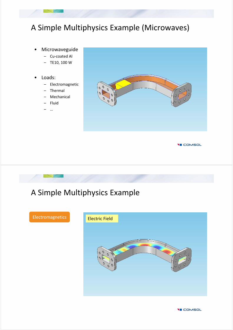
• Microwaveguide– Cu‐coated Al
– TE10, 100 W
• Loads:– Electromagnetic
– Thermal
– Mechanical
– Fluid
– …
A Simple Multiphysics Example (Microwaves)
A Simple Multiphysics Example
Electromagnetics Electric Field
A Simple Multiphysics Example
Electromagnetics
Heat Transfer
)(jQ )(T
Temperature
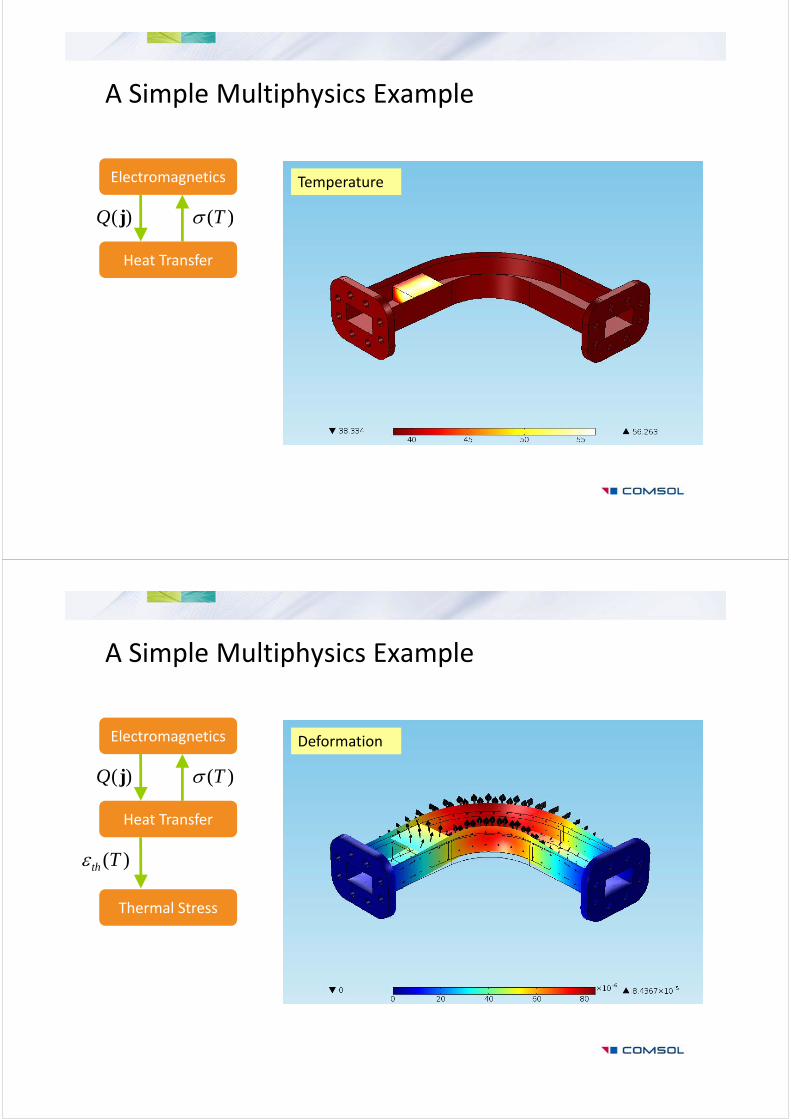
A Simple Multiphysics Example
Electromagnetics
Heat Transfer
Thermal Stress
)(jQ )(T
)(Tth
Deformation
A Simple Multiphysics Example
Electromagnetics
Heat Transfer
Thermal Stress
Fluid Flow
)(jQ )(T
)(Tth
)(T TCp v
Velocity and Temperature
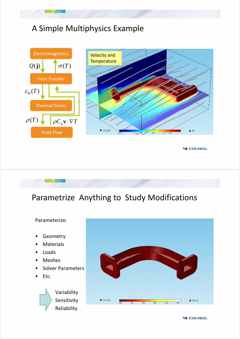
Parametrize Anything to Study Modifications
Parameterize:
• Geometry
• Materials
• Loads
• Meshes
• Solver Parameters
• Etc.
Variability
Sensitivity
Reliability
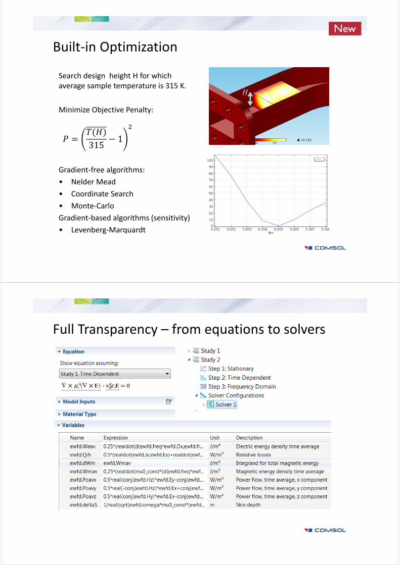
Built‐in Optimization
Search design height H for which average sample temperature is 315 K.
Minimize Objective Penalty:
Gradient‐free algorithms:
• Nelder Mead
• Coordinate Search
• Monte‐Carlo
Gradient‐based algorithms (sensitivity)
• Levenberg‐Marquardt
3151
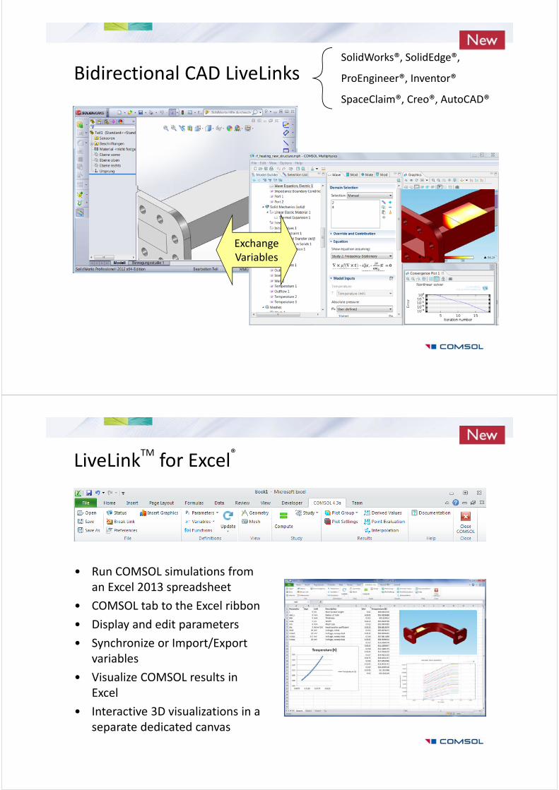
Full Transparency – from equations to solvers
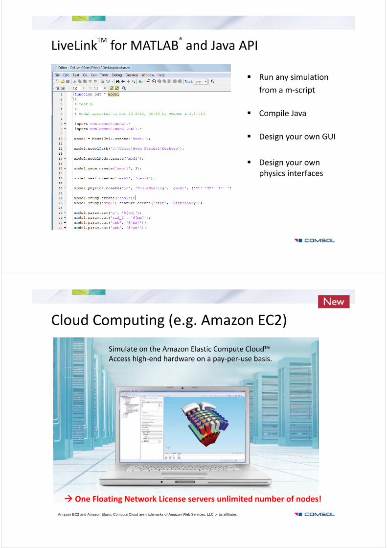
Bidirectional CAD LiveLinksSolidWorks®, SolidEdge®,
ProEngineer®, Inventor®
SpaceClaim®, Creo®, AutoCAD®
ExchangeVariables
LiveLinkTMfor Excel
®
• Run COMSOL simulations from an Excel 2013 spreadsheet
• COMSOL tab to the Excel ribbon
• Display and edit parameters
• Synchronize or Import/Export variables
• Visualize COMSOL results in Excel
• Interactive 3D visualizations in a separate dedicated canvas
Run any simulation
from a m‐script
Compile Java
Design your own GUI
Design your own physics interfaces
LiveLinkTMfor MATLAB
®and Java API
Simulate on the Amazon Elastic Compute Cloud™ Access high‐end hardware on a pay‐per‐use basis.
Cloud Computing (e.g. Amazon EC2)
One Floating Network License servers unlimited number of nodes!
Amazon EC2 and Amazon Elastic Compute Cloud are trademarks of Amazon Web Services, LLC or its affiliates.
The New Optical Waves Module
• Extension of COMSOL for EM problems at optical wavelengths (nm‐μm)
– Optical fibers , Photonic waveguides , Photonic crystals , Nonlinear optics
– Laser resonator design , Active devices in photonics
• Includes simulations of domains that are much larger than the wavelength (unlike RF Module) by Beam Envelope Method
– Directional couplers,
– fiber Bragg gratings,
– second harmonic generation,
– self‐phase modulation etc.
Wave Optics Module
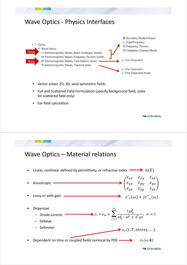
Wave Optics ‐ Physics Interfaces
New
New
• Vector solver 2D, 3D, axial symmetric fields
• Full and Scattered Field Formulation (specify background field, solve for scattered field only)
• Far‐field calculation
Wave Optics – Material relations
• Linear, nonlinear defined by permittivity, or refractive index
• Anisotropic
• Lossy or with gain
• Dispersive
– Drude‐Lorentz
– Debeye
– Sellmeier
• Dependent on time or coupled fields nonlocal by PDE
, , , …
,
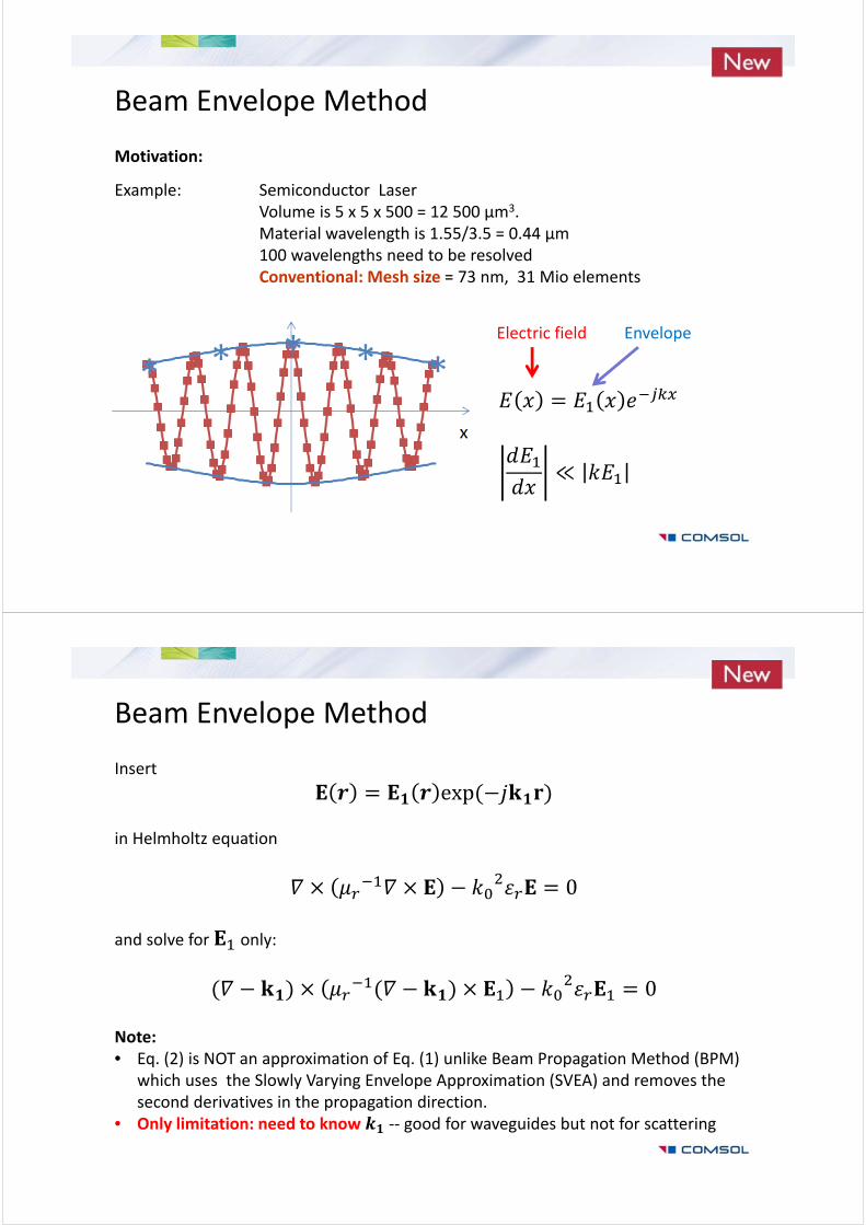
Beam Envelope Method
Motivation:
Example: Semiconductor LaserVolume is 5 x 5 x 500 = 12 500 µm3.Material wavelength is 1.55/3.5 = 0.44 µm 100 wavelengths need to be resolved Conventional: Mesh size = 73 nm, 31 Mio elements
Electric field Envelope
≪
Beam Envelope Method
Insert
exp
in Helmholtz equation
0
and solve for only:
0
Note:• Eq. (2) is NOT an approximation of Eq. (1) unlike Beam Propagation Method (BPM)
which uses the Slowly Varying Envelope Approximation (SVEA) and removes the second derivatives in the propagation direction.
• Only limitation: need to know ‐‐ good for waveguides but not for scattering
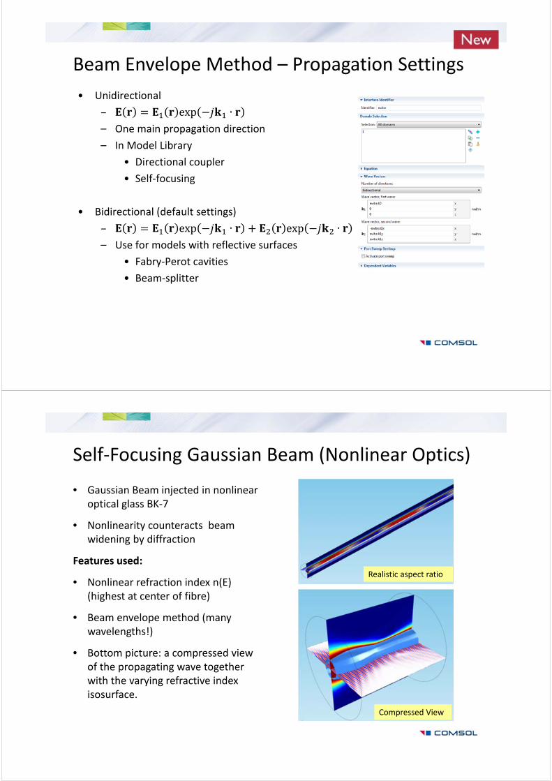
Beam Envelope Method – Propagation Settings
• Unidirectional
– exp ∙– One main propagation direction
– In Model Library
• Directional coupler
• Self‐focusing
• Bidirectional (default settings)
– exp ∙ exp ∙– Use for models with reflective surfaces
• Fabry‐Perot cavities
• Beam‐splitter
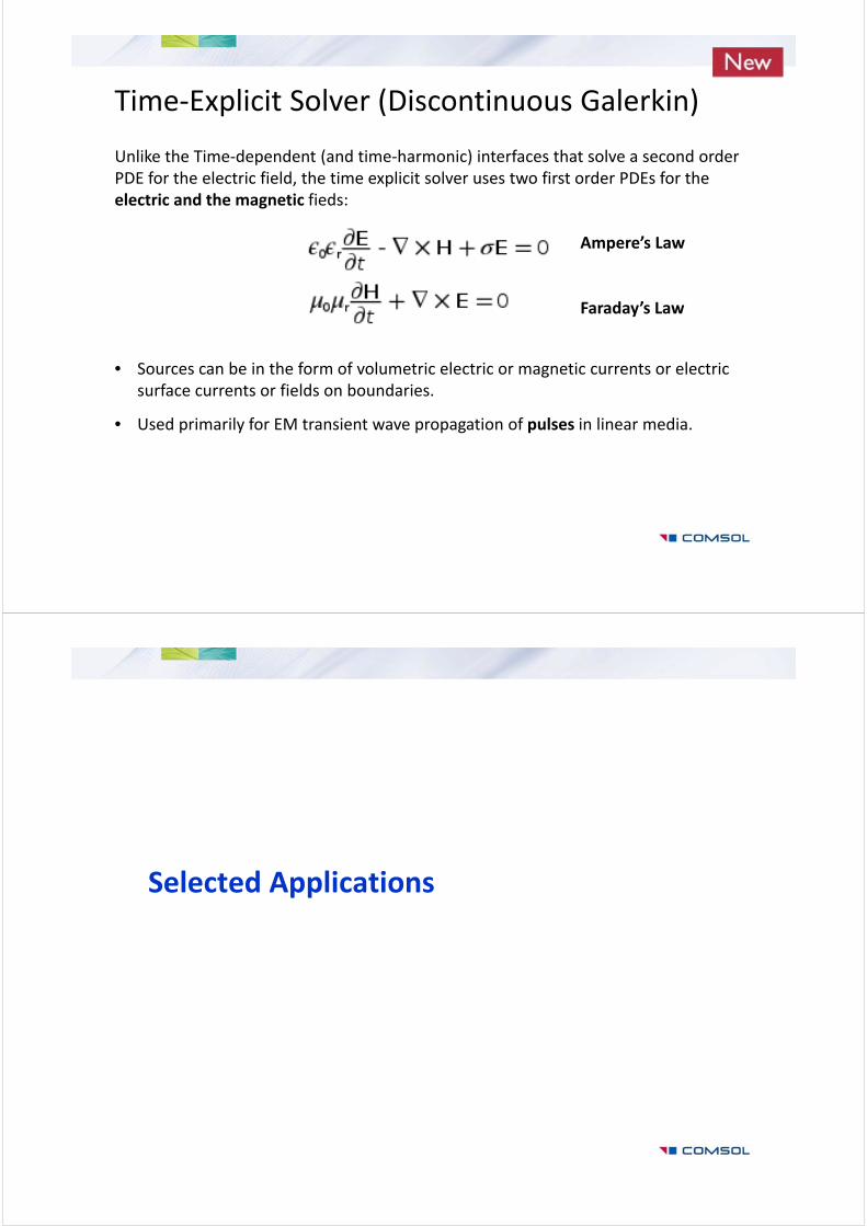
Self‐Focusing Gaussian Beam (Nonlinear Optics)
• Gaussian Beam injected in nonlinear optical glass BK‐7
• Nonlinearity counteracts beam widening by diffraction
Features used:
• Nonlinear refraction index n(E) (highest at center of fibre)
• Beam envelope method (many wavelengths!)
• Bottom picture: a compressed view of the propagating wave together with the varying refractive index isosurface.
Realistic aspect ratio
Compressed View
Time‐Explicit Solver (Discontinuous Galerkin)
Unlike the Time‐dependent (and time‐harmonic) interfaces that solve a second order PDE for the electric field, the time explicit solver uses two first order PDEs for the electric and the magnetic fieds:
• Sources can be in the form of volumetric electric or magnetic currents or electric surface currents or fields on boundaries.
• Used primarily for EM transient wave propagation of pulses in linear media.
Ampere’s Law
Faraday’s Law
Selected Applications
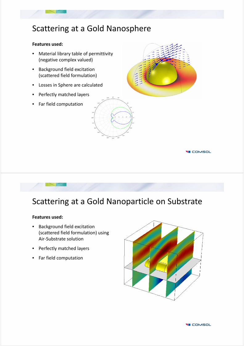
Scattering at a Gold Nanosphere
Features used:
• Material library table of permittivity (negative complex valued)
• Background field excitation (scattered field formulation)
• Losses in Sphere are calculated
• Perfectly matched layers
• Far field computation
Scattering at a Gold Nanoparticle on Substrate
Features used:
• Background field excitation (scattered field formulation) using Air‐Substrate solution
• Perfectly matched layers
• Far field computation
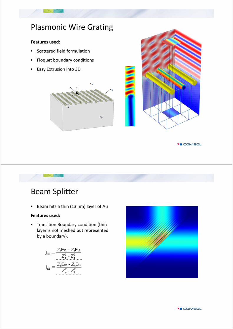
Plasmonic Wire Grating
Features used:
• Scattered field formulation
• Floquet boundary conditions
• Easy Extrusion into 3D
Beam Splitter
• Beam hits a thin (13 nm) layer of Au
Features used:
• Transition Boundary condition (thin layer is not meshed but represented by a boundary).
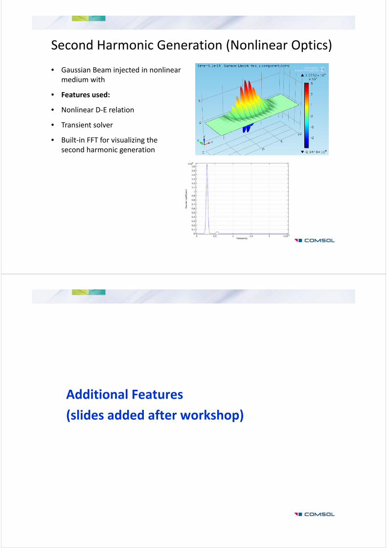
Second Harmonic Generation (Nonlinear Optics)
• Gaussian Beam injected in nonlinear medium with
• Features used:
• Nonlinear D‐E relation
• Transient solver
• Built‐in FFT for visualizing the second harmonic generation
Additional Features
(slides added after workshop)
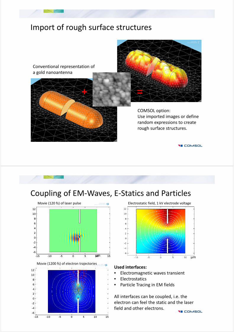
Import of rough surface structures
COMSOL option:Use imported images or definerandom expressions to create rough surface structures.
Conventional representation ofa gold nanoantenna
+ =
Coupling of EM‐Waves, E‐Statics and ParticlesMovie (120 fs) of laser pulse Electrostatic field, 1 kV electrode voltage
Movie (1200 fs) of electron trajectories
μm μm
Used interfaces:• Electromagnetic waves transient• Electrostatics• Particle Tracing in EM fields
All interfaces can be coupled, i.e. the electron can feel the static and the laser field and other electrons.
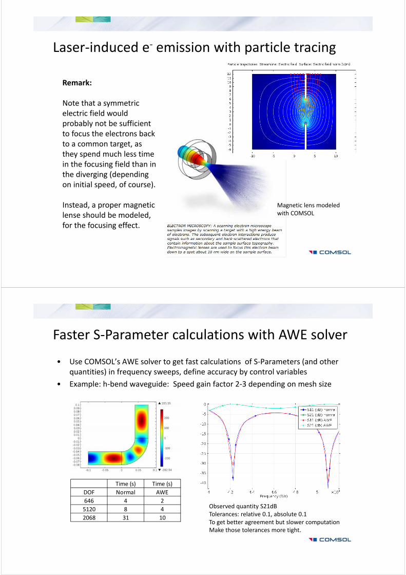
Laser‐induced e‐ emission with particle tracing
Remark:
Note that a symmetric electric field would probably not be sufficient to focus the electrons back to a common target, as they spend much less time in the focusing field than in the diverging (depending on initial speed, of course).
Instead, a proper magnetic lense should be modeled, for the focusing effect.
Magnetic lens modeledwith COMSOL
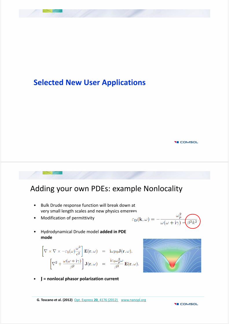
Faster S‐Parameter calculations with AWE solver
• Use COMSOL’s AWE solver to get fast calculations of S‐Parameters (and other quantities) in frequency sweeps, define accuracy by control variables
• Example: h‐bend waveguide: Speed gain factor 2‐3 depending on mesh size
Time (s) Time (s)
DOF Normal AWE
646 4 2
5120 8 4
2068 31 10
Observed quantity S21dBTolerances: relative 0.1, absolute 0.1To get better agreement but slower computationMake those tolerances more tight.
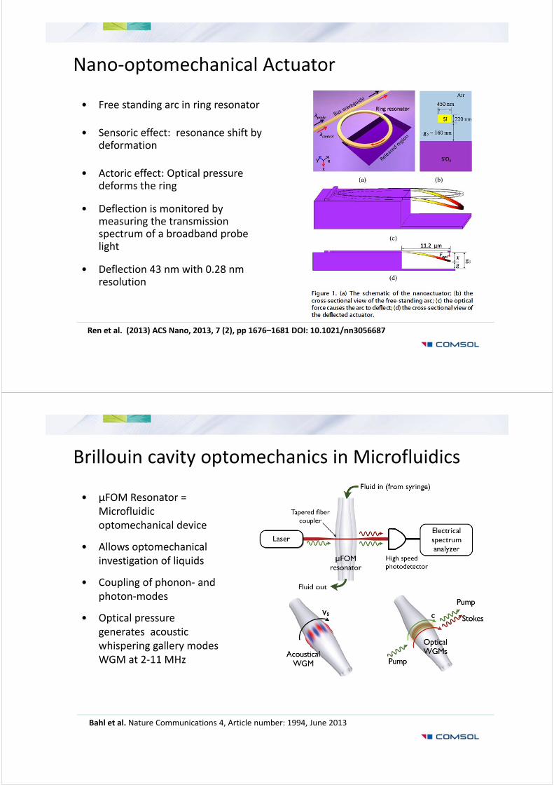
Selected New User Applications
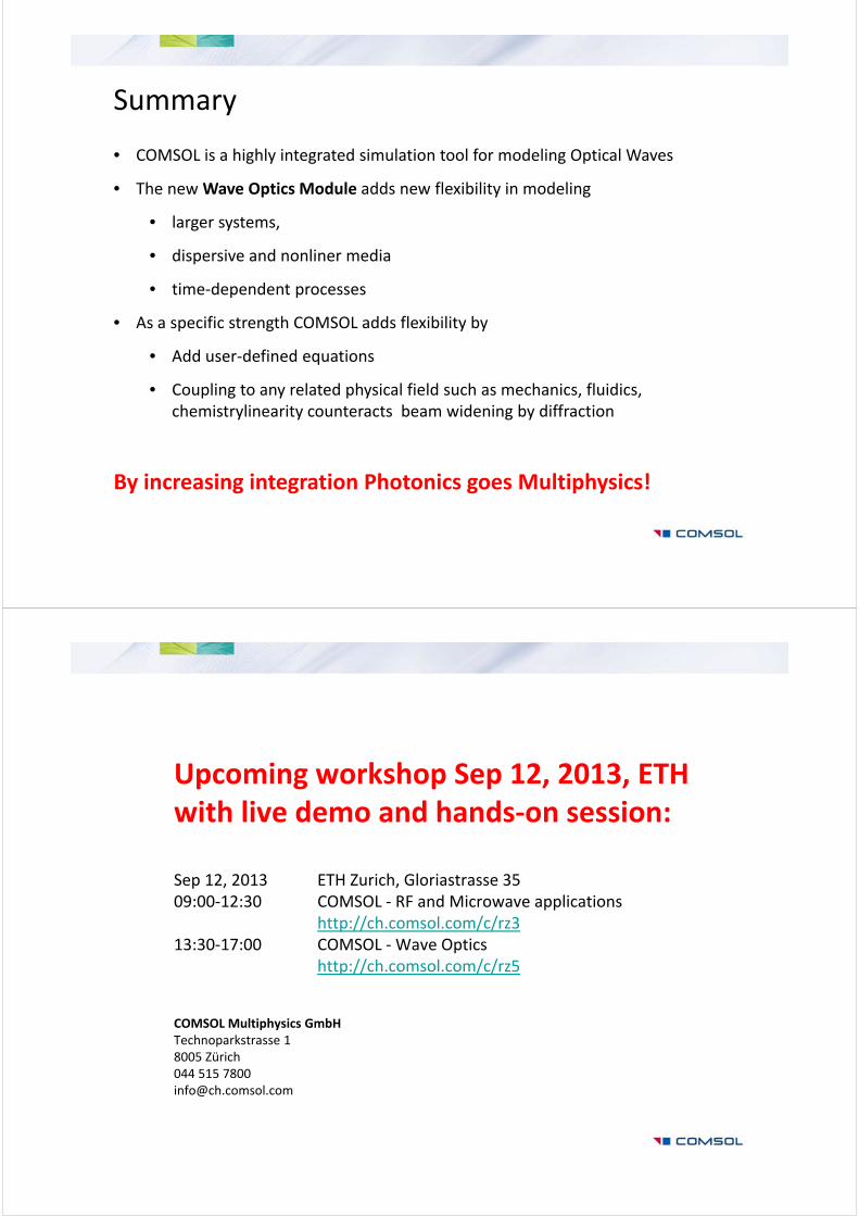
• Bulk Drude response function will break down at very small length scales and new physics emerges
• Modification of permittivity
• Hydrodynamical Drude model added in PDE mode
• = nonlocal phasor polarization current
Adding your own PDEs: example Nonlocality
G. Toscano et al. (2012) Opt. Express 20, 4176 (2012) www.nanopl.org
• Free standing arc in ring resonator
• Sensoric effect: resonance shift bydeformation
• Actoric effect: Optical pressuredeforms the ring
• Deflection is monitored by measuring the transmission spectrum of a broadband probe light
• Deflection 43 nm with 0.28 nm resolution
Nano‐optomechanical Actuator
Ren et al. (2013) ACS Nano, 2013, 7 (2), pp 1676–1681 DOI: 10.1021/nn3056687
• μFOM Resonator = Microfluidic optomechanical device
• Allows optomechanicalinvestigation of liquids
• Coupling of phonon‐ and photon‐modes
• Optical pressure generates acoustic whispering gallery modes WGM at 2‐11 MHz
Brillouin cavity optomechanics in Microfluidics
Bahl et al. Nature Communications 4, Article number: 1994, June 2013
Summary
• COMSOL is a highly integrated simulation tool for modeling Optical Waves
• The new Wave Optics Module adds new flexibility in modeling
• larger systems,
• dispersive and nonliner media
• time‐dependent processes
• As a specific strength COMSOL adds flexibility by
• Add user‐defined equations
• Coupling to any related physical field such as mechanics, fluidics, chemistrylinearity counteracts beam widening by diffraction
By increasing integration Photonics goes Multiphysics!
Upcoming workshop Sep 12, 2013, ETH with live demo and hands‐on session:
Sep 12, 2013 ETH Zurich, Gloriastrasse 3509:00‐12:30 COMSOL ‐ RF and Microwave applications
http://ch.comsol.com/c/rz313:30‐17:00 COMSOL ‐Wave Optics
http://ch.comsol.com/c/rz5
COMSOL Multiphysics GmbHTechnoparkstrasse 18005 Zürich044 515 [email protected]