Embed Size (px)
Citation preview
Crystalline, Rare-Earth-doped
Sesquioxide and YAG
PLD-Films
Dissertation
zur Erlangung des Doktorgradesdes Departments Physikder Universität Hamburg
vorgelegt vonYury Kuzminykh
aus Minsk
Hamburg2006
Gutachter der Dissertation: Prof. Dr. G. HuberProf. Dr. D. Heitmann
Gutachter der Disputation: Prof. Dr. G. HuberProf. Dr. K. Sengstock
Datum der Disputation: 11.04.2006
Vorsitzender des Prüfungsausschusses: Dr. K. Petermann
Dekan der Fakultät für Mathematik, Informatik und Naturwissenschaften: Prof. Dr. A. Frühwald
Vorsitzender des Promotionsausschusses: Prof. Dr. G. Huber
III
Abstract
Yury Kuzminykh, Crystalline, Rare-Earth-doped Sesquioxide and YAG PLD-Films
This thesis presents the results of fabrication as well as structural andspectroscopic characterization of pulsed-laser-deposited oxide films. Thefabricated films are activated by rare-earth ions and proven to be crystalline.Such films are promising for the fabrication of integrated optical devices orcompact light sources. The application as active medium for thin disk lasers isconsidered as well.
The films produced include scandia (Sc2O3), yttria (Y2O3), lutetia (Lu2O3),ytterbia (Yb2O3) and yttrium-aluminum garnet (Y3Al5O12) films with thicknessesin the range from 500 nm to 10 μm. Their structural properties have beeninvestigated by means of X-ray diffraction. The influence of the depositionparameters on the characteristics of the scandia films has been investigated inmore detail and the optimal deposition parameters have been determined.
The scandia films are highly textured along the <111>-direction and thecrystallite dimensions reach several hundreds of nanometers. The lutetia filmsdeposited under the same conditions demonstrate substantially smallercrystallites (<50 nm), which are mostly <111>-oriented. However, otherorientations are also present in the diffraction patterns of the lutetia films.
The YAG films deposited at 700°C have been proven to be amorphous. Afterannealing at 1200°C the XRD analysis revealed a polycrystalline behavior of theYb:YAG films and their spectroscopic properties resembled those of the bulk.
Waveguiding has been demonstrated in a 1.2 μm thick Eu:Y2O3 film as well asin 3 μm and 10 μm thick Nd:Sc2O3 films. The light propagation losses have beenestimated to be 19.5 dB·cm-1 and 12 dB·cm-1, respectively, for the 3 μm and10 μm Nd:Sc2O3 films. The excitation and emission spectra for the Nd:Sc2O3
films are close to those of the bulk material. The lifetime of the 4F3/2(Nd3+)multiplet in the scandia PLD-film is somewhat reduced compared to that in thebulk material.
Spectroscopic investigations of ytterbia as well as Yb-doped scandia, lutetia,and YAG films have been performed. For the ytterbia films the emission hasonly been detected at temperatures below 20 K. The spectra of the Yb:Sc2O3
and Yb:Lu2O3 films are bulk-like and vary slightly depending on the usedsubstrate and the post annealing treatment (at 900°C). The luminescencequantum efficiency was up to 66% or up to 78%, respectively for the Yb-dopedlutetia and scandia films.
IV
Kurzfassung
Yury Kuzminykh, Kristalline, Selten-Erd-dotierte Sesquioxid- und YAG-PLD-Schichten
Diese Arbeit präsentiert die Ergebnisse der Herstellung, sowie der strukturellenund spektroskopischen Untersuchungen der mittels Pulsed Laser Depositionhergestellten oxidischen Schichten. Die Schichten sind mit Selten-Erd-Ionendotiert und weisen kristalline Struktur auf. Derartige Schichten könnenAnwendungen im Bereich der integrierte Optik finden. Auch der Einsatz alsaktive Materialien für kompakte Lichtquellen und in Scheibenlasern ist möglich.
Es wurden Schichten mit Dicken im Bereich von 500 nm bis 10 μm aus denfolgenden Materialien hergestellt: Scandium- (Sc2O3), Yttrium- (Y2O3),Lutetium- (Lu2O3) und Ytterbiumoxid (Yb2O3) sowie Yttrium-Aluminium-Granat (Y3Al5O12). Die Struktur der Schichten wurde mittels Röntgenbeugung(XRD) untersucht. Für die Scandiumoxidschichten wurde der Einfluss derHerstellungsparameter auf die Schichteigenschaften untersucht.
Die Scandiumoxidschichten sind stark in <111>-Richtung orientiert und weisenKristallitgrößen von einigen hundert Nanometern auf. Die Kristallite in untergleichen Bedingungen hergestellten Lutetiumoxidschichten sind dagegen kleiner50 nm. Die meisten dieser Kristallite sind <111>-orientiert, aber auch andereOrientierungen treten auf.
Die bei 700°C hergestellten YAG-Schichten sind amorph. Nach dem Tempernbei 1200°C haben XRD-Untersuchungen die polykristalline Struktur derSchichten bestätigt. Ihr spektrales Verhalten war ähnlich zu dem des entspre-chenden Volumenkristalls.
Wellenleitung wurde in der 1.2 μm dicken Eu:Y2O3-Schicht sowie in den 3 μmund 10 μm dicken Nd:Sc2O3-Schichten experimentell nachgewiesen. Lichtaus-breitungsverluste von 19.5 dB·cm-1 bzw. 12 dB·cm-1 wurden für die 3 μm bzw.10 μm Wellenleitern ermittelt. Die Anregungs- und Emissionsspektren derNd-dotierten Schichten ähneln denen des Volumenkristalls, wobei die Lebens-dauer des 4F3/2(Nd3+)-Multipletts in den Schichten etwas verkürzt ist.
Für die Ytterbiumoxidschichten ist die Emission nur bei Temperaturen unter20 K gemessen worden. Die spektroskopischen Untersuchungen der Ytterbium-dotierten Scandium- und Lutetiumoxidschichten zeigen, dass deren Spektrendenen der Volumenkristalle entsprechen, aber leicht von dem verwendetenSubstrat und dem Nachtempern (900°C) abhängen. Die Lumineszenzquanten-effizienz erreicht den Wert von 66% für die Yb:Lu2O3 und 78% für die Yb:Sc2O3
Schichten.
V
Contents
Abstract........................................................................................................III
Kurzfassung...................................................................................................IV
Index of Figures..........................................................................................VIII
Index of Tables...........................................................................................XIII
List of Symbols and Abbreviations.............................................................XIV
Chapter 1. Introduction..............................................................................1
§1.1 Motivation................................................................................................1
§1.2 Overview and Structure of this Thesis.....................................................4
Chapter 2. Materials...................................................................................6
§2.1 Sesquioxides..............................................................................................6
2.1.1 Growth of Sesquioxide Crystals..........................................................8
§2.2 Yttrium-Aluminum Garnet.....................................................................10
§2.3 Corundum (Sapphire).............................................................................11
§2.4 Quartz....................................................................................................12
§2.5 Summary of Material Properties............................................................13
Chapter 3. Analytical Techniques.............................................................15
§3.1 X-Ray Diffraction...................................................................................15
§3.2 Ellipsometry and Reflectometry.............................................................20
§3.3 Scattering Measurements........................................................................25
§3.4 Spectroscopic Measurements...................................................................26
VI
Chapter 4. Film Preparation by Pulsed Laser Deposition........................31
§4.1 Deposition Techniques............................................................................31
4.1.1 Overview...........................................................................................31
4.1.2 Pulsed Laser Deposition Technique...................................................36
§4.2 Preparation of PLD-Films......................................................................39
§4.3 Optimization of PLD Process Parameters..............................................44
4.3.1 Laser and Target...............................................................................45
4.3.2 Substrate...........................................................................................47
4.3.3 Background Atmosphere...................................................................52
4.3.4 Summary and Discussion..................................................................55
Chapter 5. X-ray Diffraction Analysis......................................................58
§5.1 Ytterbia Films........................................................................................58
§5.2 YAG Films..............................................................................................60
§5.3 Lutetia and Scandia Films......................................................................62
§5.4 Summary and Discussion........................................................................67
Chapter 6. Waveguiding Sesquioxide PLD-Films......................................70
§6.1 Introduction............................................................................................70
6.1.1 Theory of Waveguiding.....................................................................72
§6.2 Eu-doped Yttria Waveguide...................................................................75
6.2.1 Optical Spectroscopy.........................................................................75
6.2.2 Waveguiding Experiments.................................................................77
§6.3 Nd-doped Scandia Waveguides...............................................................79
6.3.1 Optical Spectroscopy ........................................................................80
6.3.2 Lifetime Measurements.....................................................................82
6.3.3 Waveguiding Experiments.................................................................83
6.3.4 Propagation Losses............................................................................86
VII
§6.4 Structuring Experiments........................................................................89
6.4.1 Lift-off Technique..............................................................................89
6.4.2 Ion-Beam Etching.............................................................................91
§6.5 Summary and Discussion........................................................................91
Chapter 7. Ytterbium-Doped PLD-Films.................................................93
§7.1 Introduction............................................................................................93
7.1.1 Thin Disk Laser Concept..................................................................93
7.1.2 Microcavities.....................................................................................96
7.1.3 Ytterbium-Doped Materials..............................................................98
§7.2 Characterization of Yb-Doped PLD-films.............................................101
7.2.1 Ytterbia Films.................................................................................101
7.2.2 Yb-doped Sesquioxide Films............................................................103
7.2.3 Yb-doped YAG Films......................................................................108
§7.3 Summary and Discussion......................................................................111
Chapter 8. Conclusions...........................................................................113
§8.1 Summary of Results..............................................................................113
§8.2 Resumé and Outlook............................................................................115
Appendix A. List of Deposited Films......................................................117
Appendix B. Fresnel Equations...............................................................119
Bibliography.................................................................................................120
Acknowledgments.........................................................................................129
VIII
Index of Figures
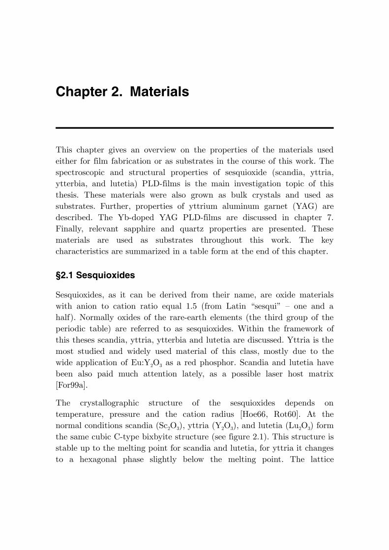
Figure 2.1: Crystal structure of cubic sesquioxides viewed nearly in <100>-direction. (white – O2-, gray – RE3+(C2), dark gray – RE3+(C3i)).. .7
Figure 2.2: Scheme of the HEM crystal growth set-up.........................................9
Figure 3.1: X-ray diffraction on crystal lattice...................................................15
Figure 3.2: (a) θ-2θ scan – domains with different interplane distances detected;(b) ω-scan (rocking curve) – domains with certain interplanedistance and different orientations detected..................................16
Figure 3.3: Rocking curve of the <222> diffraction peak for the 500 nm Sc2O3
PLD-film on α-Al2O3 substrate.....................................................19
Figure 3.4: High resolution scan of the <222> diffraction peak for the Sc2O3
crystal...........................................................................................19
Figure 3.5: Reflection of light from layered structure.........................................21
Figure 3.6: Polarization state of light described with ellipticity and orientation..............................................................................22
Figure 3.7: Ellipsometer.....................................................................................23
Figure 3.8: Scheme of ellipsometric measurement..............................................24
Figure 3.9: Experimental set-up used for the scattering measurements usingintegrating (Ulbricht) sphere.........................................................25
Figure 3.10: Scheme of experimental set-up for the spectroscopic measurements in near- infrared region..........................................27
Figure 3.11: Scheme of Fluorolog spectrometer set-up.......................................28
Figure 3.12: Scheme of experimental set-up for the fluorescence lifetimemeasurements................................................................................29
Figure 4.1: Pulsed laser deposition machine.......................................................40
Figure 4.2: Reflectometer signal recorded in situ during deposition of a 1 μm thick Sc2O3 film.............................................................44
IX
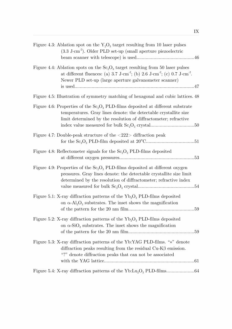
Figure 4.3: Ablation spot on the Y2O3 target resulting from 10 laser pulses(3.3 J⋅cm-2). Older PLD set-up (small aperture piezoelectricbeam scanner with telescope) is used............................................46
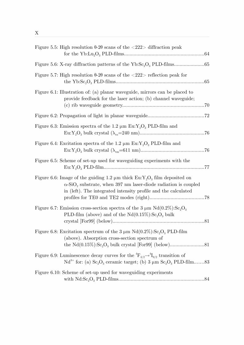
Figure 4.4: Ablation spots on the Sc2O3 target resulting from 50 laser pulsesat different fluences: (a) 3.7 J⋅cm-2; (b) 2.6 J⋅cm-2; (c) 0.7 J⋅cm-2.Newer PLD set-up (large aperture galvanometer scanner)is used...........................................................................................47
Figure 4.5: Illustration of symmetry matching of hexagonal and cubic lattices. 48
Figure 4.6: Properties of the Sc2O3 PLD-films deposited at different substratetemperatures. Gray lines denote: the detectable crystallite sizelimit determined by the resolution of diffractometer; refractiveindex value measured for bulk Sc2O3 crystal.................................50
Figure 4.7: Double-peak structure of the <222> diffraction peak for the Sc2O3 PLD-film deposited at 20°C.....................................51
Figure 4.8: Reflectometer signals for the Sc2O3 PLD-films deposited at different oxygen pressures.........................................................53
Figure 4.9: Properties of the Sc2O3 PLD-films deposited at different oxygenpressures. Gray lines denote: the detectable crystallite size limitdetermined by the resolution of diffractometer; refractive indexvalue measured for bulk Sc2O3 crystal...........................................54
Figure 5.1: X-ray diffraction patterns of the Yb2O3 PLD-films deposited on α-Al2O3 substrates. The inset shows the magnification of the pattern for the 20 nm film..................................................59
Figure 5.2: X-ray diffraction patterns of the Yb2O3 PLD-films deposited on α-SiO2 substrates. The inset shows the magnification of the pattern for the 20 nm film..................................................59
Figure 5.3: X-ray diffraction patterns of the Yb:YAG PLD-films. “∗” denotediffraction peaks resulting from the residual Cu-Kβ emission. “?” denote diffraction peaks that can not be associated with the YAG lattice.....................................................................61
Figure 5.4: X-ray diffraction patterns of the Yb:Lu2O3 PLD-films.....................64
X
Figure 5.5: High resolution θ-2θ scans of the <222> diffraction peakfor the Yb:Lu2O3 PLD-films..........................................................64
Figure 5.6: X-ray diffraction patterns of the Yb:Sc2O3 PLD-films......................65
Figure 5.7: High resolution θ-2θ scans of the <222> reflection peak for the Yb:Sc2O3 PLD-films................................................................65
Figure 6.1: Illustration of: (a) planar waveguide, mirrors can be placed toprovide feedback for the laser action; (b) channel waveguide; (c) rib waveguide geometry...........................................................70
Figure 6.2: Propagation of light in planar waveguide.........................................72
Figure 6.3: Emission spectra of the 1.2 μm Eu:Y2O3 PLD-film and Eu:Y2O3 bulk crystal (λex=240 nm)...............................................76
Figure 6.4: Excitation spectra of the 1.2 μm Eu:Y2O3 PLD-film and Eu:Y2O3 bulk crystal (λem=611 nm)..............................................76
Figure 6.5: Scheme of set-up used for waveguiding experiments with theEu:Y2O3 PLD-film.........................................................................77
Figure 6.6: Image of the guiding 1.2 μm thick Eu:Y2O3 film deposited on α-SiO2 substrate, when 397 nm laser-diode radiation is coupled in (left). The integrated intensity profile and the calculated profiles for TE0 and TE2 modes (right).......................................78
Figure 6.7: Emission cross-section spectra of the 3 μm Nd(0.2%):Sc2O3 PLD-film (above) and of the Nd(0.15%):Sc2O3 bulk crystal [For99] (below)..................................................................81
Figure 6.8: Excitation spectrum of the 3 μm Nd(0.2%):Sc2O3 PLD-film (above). Absorption cross-section spectrum of the Nd(0.15%):Sc2O3 bulk crystal [For99] (below).........................81
Figure 6.9: Luminescence decay curves for the 4F3/2→4I9/2 transition of
Nd3+ for: (a) Sc2O3 ceramic target; (b) 3 μm Sc2O3 PLD-film.......83
Figure 6.10: Scheme of set-up used for waveguiding experiments with Nd:Sc2O3 PLD-films..............................................................84
XI
Figure 6.11: Image of the waveguiding 3 μm PLD-film and the integratedintensity profile compared to calculated TE0 and TE2 modeprofiles (above). Image of the waveguiding 10 μm film and theintegrated intensity profile (below) (approximately the samemagnification as the image above, exact scale not determined)....85
Figure 6.12: Simulated reflectometer signal curves for: (a) “no losses” model; (b) scattering in film volume; (c) scattering at film surface. (d) Reflectometer signal recorded experimentally during deposition of the 10 μm Nd:Sc2O3 PLD-film.................................88
Figure 6.13: Scheme of the lift-off technique: (a) two layers of photoresist aredeposited; (b) photoresist is exposed through a mask anddeveloped; (c) Y2O3 is deposited by PLD process; (d) photoresist is removed together with Y2O3 on it.....................90
Figure 6.14: Scheme of the Ar+-beam etching process: (a) Y2O3 PLD-film isdeposited, (b) photoresist is deposited on top; (c) photoresist isexposed through a mask and developed; (d) Y2O3 is etched with Ar+-beam; (e) photoresist is removed...................................90
Figure 6.15: SEM image of the Eu:Y2O3 stripes on sapphire substrate produced by the lift-off technique.................................................90
Figure 6.16: SEM image of step in the Eu:Y2O3 PLD-film produced byAr+-beam etching..........................................................................90
Figure 7.1: Thin disk laser set-up (above). Laser head design (below, left).Pump beam reflections scheme for 16x passes – 8x forward and 8x backward (below, right)....................................................94
Figure 7.2: (a) model of a microcavity, dark gray – high refractive indexmaterial, light gray – low refractive index material; black – activemedium should be placed here; (b) refractive index profile; (c) strength of electric field, normalized to the incident light.......97
Figure 7.3: Illustration of energy migration model in highly Yb-doped materials......................................................................................100
Figure 7.4: Low temperature emission spectra of the 500 nm Yb2O3 film on α-SiO2 substrate under 220 nm excitation...................................102
XII
Figure 7.5: Broadband visible emission of the 500 nm Yb2O3 film on α-SiO2
substrate detected under 220 nm (5.6 eV) excitation (T=9K)....103
Figure 7.6: Excitation (left, λem=1030 nm) and emission cross-section (right,λex=902.5 nm) spectra of the Yb:Lu2O3 PLD-films. Yb:Lu2O3 bulk crystal emission and absorption spectra [Pet01] presented for comparison.............................................................................106
Figure 7.7: Excitation (left, λem=1042 nm ) and emission cross-section (right,λex=893.5 nm) spectra of the Yb:Sc2O3 PLD-films. Yb:Sc2O3 bulkcrystal emission and absorption spectra [Pet01] presented forcomparison..................................................................................107
Figure 7.8: Excitation (left, λem=1020-1030 nm) and emission cross-section(right, λex=915-930 nm) spectra of the Yb:YAG PLD-films.Yb:YAG and Yb:Y2O3 bulk crystal emission and absorptionspectra [Pet01] are presented for comparison..............................110
XIII
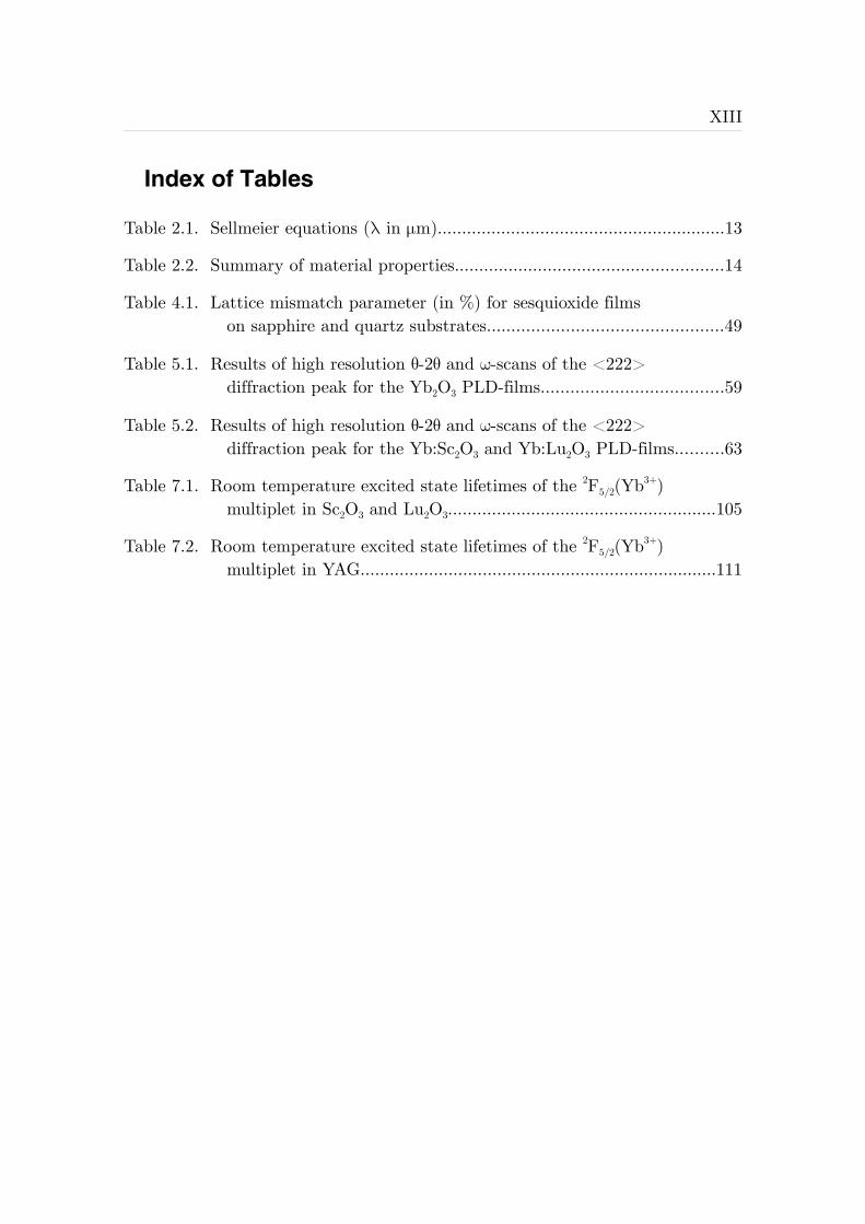
Index of Tables
Table 2.1. Sellmeier equations (λ in μm)...........................................................13
Table 2.2. Summary of material properties.......................................................14
Table 4.1. Lattice mismatch parameter (in %) for sesquioxide films on sapphire and quartz substrates................................................49
Table 5.1. Results of high resolution θ-2θ and ω-scans of the <222> diffraction peak for the Yb2O3 PLD-films.....................................59
Table 5.2. Results of high resolution θ-2θ and ω-scans of the <222> diffraction peak for the Yb:Sc2O3 and Yb:Lu2O3 PLD-films..........63
Table 7.1. Room temperature excited state lifetimes of the 2F5/2(Yb3+) multiplet in Sc2O3 and Lu2O3.......................................................105
Table 7.2. Room temperature excited state lifetimes of the 2F5/2(Yb3+) multiplet in YAG.........................................................................111
XIV
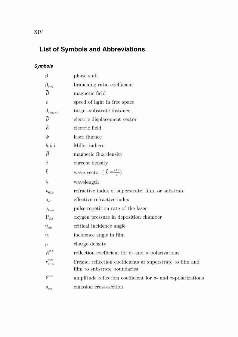
List of Symbols and Abbreviations
Symbols
β phase shift
βi→j branching ratio coefficientB magnetic field
c speed of light in free space
dtarg-sub target-substrate distanceD electric displacement vectorE electric field
Φ laser fluence
h,k,l Miller indicesH magnetic flux densityj current density
k wave vector (∣k∣=2πn
λ)
λ wavelength
n0,f,s refractive index of superstrate, film, or substrate
neff effective refractive index
νlaser pulse repetition rate of the laser
PO2 oxygen pressure in deposition chamber
θcrit critical incidence angle
θf incidence angle in film
ρ charge density
Rσ,π reflection coefficient for σ- and π-polarizations
r 0f , fsσ,π Fresnel reflection coefficients at superstrate to film and
film to substrate boundaries
r σ,π amplitude reflection coefficient for σ- and π-polarizations
σem emission cross-section
XV
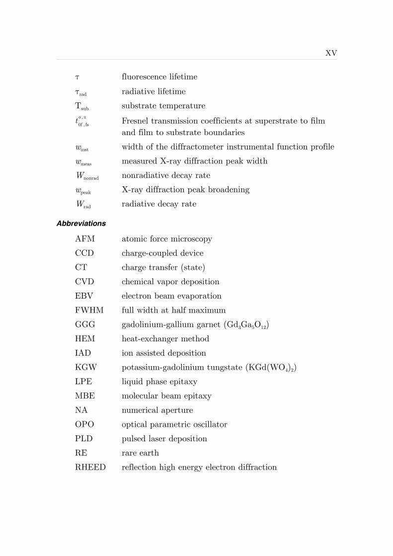
τ fluorescence lifetime
τrad radiative lifetime
Tsub substrate temperature
t 0f , fsσ,π Fresnel transmission coefficients at superstrate to film
and film to substrate boundaries
winst width of the diffractometer instrumental function profile
wmeas measured X-ray diffraction peak width
Wnonrad nonradiative decay rate
wpeak X-ray diffraction peak broadening
Wrad radiative decay rate
Abbreviations
AFM atomic force microscopy
CCD charge-coupled device
CT charge transfer (state)
CVD chemical vapor deposition
EBV electron beam evaporation
FWHM full width at half maximum
GGG gadolinium-gallium garnet (Gd3Ga5O12)
HEM heat-exchanger method
IAD ion assisted deposition
KGW potassium-gadolinium tungstate (KGd(WO4)2)
LPE liquid phase epitaxy
MBE molecular beam epitaxy
NA numerical aperture
OPO optical parametric oscillator
PLD pulsed laser deposition
RE rare earth
RHEED reflection high energy electron diffraction
XVI
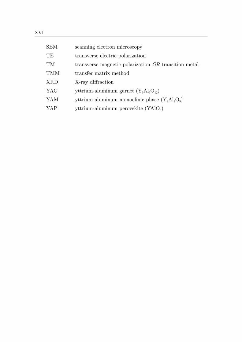
SEM scanning electron microscopy
TE transverse electric polarization
TM transverse magnetic polarization OR transition metal
TMM transfer matrix method
XRD X-ray diffraction
YAG yttrium-aluminum garnet (Y3Al5O12)
YAM yttrium-aluminum monoclinic phase (Y4Al2O9)
YAP yttrium-aluminum perovskite (YAlO3)
Chapter 1. Introduction
§1.1 Motivation
Nowadays, most of the principal optical devices – like light generators,detectors, transmitters, splitters, etc – have been demonstrated.Currently, research is focused on reducing the dimensions of these devicesand implementing them as structural elements in integrated opticalsystems. Hence, new techniques need to be developed for fabrication ofsuch systems with dimensions of the individual element down to themicrometer range. One of the possibilities is to structure or modify thevolume material, however, this approach is not flexible enough. A numberof well-established deposition techniques should be more favorable, since anumber of layers as well as several materials can be easily combined.Subsequently, the layers can be structured or deposition through a maskcan be employed in order to realize two- or three-dimensionalconfigurations.
The general tendency is to reduce the size of optical devices even ifdiscussed in other contexts than integrated optics. For example, compactlight sources are required for sensing applications, spectroscopy oranalytical techniques. From this point of view devices based onwaveguides are very promising. Possible applications of waveguiding filmsare discussed more thoroughly in chapter 6.
Lately, solid-state lasers attracted increased attention induced by theinvention of the thin disk laser set-up. This concept improves theperformance of high-power laser by decreasing the dimensions of theactive medium in order to reduce thermal stress. The typical thickness ofthe active media is, currently, in the range of several hundreds ofmicrometers, and it is desirable to utilize even thinner layers. Thus, films
2 Chapter 1
of active material with the thickness in the range of tens or hundredsmicrometers can find their application as active media in solid-state thindisk lasers. The application of deposition techniques can be especiallyfavorable in this case, since the active medium, Bragg mirrors andantireflection coatings can be fabricated as a multilayer structure in asingle process. Also periodic structures with photonic properties (e.g.microcavities) can be produced in a similar way. A more detailedintroduction into the subject of thin disk lasers and layered structures isgiven in chapter 7.
The starting point for the fabrication of the devices discussed above is thedeposition of films of a suitable material. Both the deposition techniqueand the material have to comply with some requirements. The opticalproperties of the material, as, for example, transparency in a certainwavelength range or the refractive index are important issues, but alsomechanical, chemical, or thermal properties can be critical for certainapplications. With respect to active devices, the spectroscopic propertiesof the material are to be considered as well.
Rare-earth-doped oxides are one of the most successful classes of activemedia for solid-state lasers. The only more widespread class of lasermaterials are semiconductors, which gained their popularity due to thecapability to be electrically pumped, compactness, and very lowfabrication cost. However, dielectric oxide materials demonstrate someproperties that make them advantageous for certain applications. Theyare insulators with a wide band gap and therefore transparent in the widewavelength range from ultraviolet to mid-infrared. Oxides reveal excellentchemical and mechanical properties and do not show deterioration.Another advantage follows from the difference in the operation principleof semiconductor and solid-state lasers. The absorption and emission insemiconductors results from band-to-band transitions and energy is storedin separated electrons and holes, which are not or only weakly localized.In dielectric laser media, transitions between the energy levels of a dopantion occur and, thus, the excitation states are typically localized.Exceptions can occur in the case of very high doping concentrations. Thissituation is discussed in chapter 7. Hence dielectric materials set less strict
Introduction 3
requirements for the density of defects (which can lead to undesireddeexcitation) and, consequently, for the deposition parameters and thesubstrate choice. Therefore, the required quality of the film should beeasier to achieve in this case.
Other dielectric solid-state host materials (like fluorides, borates,tungstates, vanadates, etc.), even if superior to oxides in the spectroscopicor performance characteristics, are usually inferior to them in thermalconductivity, mechanical stability or growth simplicity and scalability.This determines the prevalence of oxides as host materials in the solid-state laser domain.
A number of different techniques can be employed for the deposition ofoxide materials, including electron beam evaporation (EBV), chemicalvapor deposition (CVD), molecular beam epitaxy (MBE), ion-assisteddeposition (IAD), RF magnetron sputtering, and sol-gel methods.Recently, pulsed laser deposition (PLD) proved to be a favorabletechnique for the deposition of oxides. Its advantages are high ionizationdegree and high energy of the plasma species (up to 100 eV), whichpositively influence the films properties like density, crystallinity, andadhesion to the substrate. PLD is a very versatile technique. On the onehand it is possible to control the thickness of the film at the atomic layerscale and on the other hand pulsed-laser-deposited films with thicknessesexceeding 100 μm have been demonstrated. Adjusting the parameters ofthe process (laser wavelength, energy density, background atmosphere,substrate, etc.), the PLD technique can be adapted for the deposition of awide range of materials, going far beyond the oxides discussed in thisthesis. The material range expands from metals to multicomponentinorganic materials (like YBa2Cu3O7-x) to polymers and complex organicmolecules (like proteins). Additionally, the nonthermal character of theprocess allows to control the stoichiometry of the deposited material. Theuse of a relatively small amount of material for the target as well as thepossibility of quick change of materials or parameters makes the PLDtechnique quite convenient from the experimental point of view.
4 Chapter 1
§1.2 Overview and Structure of this Thesis
This thesis is structured in the following way. Chapter 2 gives a shortoverview of the properties of the materials used throughout this work.They include sapphire and quartz, used as substrates, as well assesquioxides (scandia, yttria, ytterbia, and lutetia) and yttrium aluminumgarnet. These materials have been used both for film fabrication and assubstrates.
Then, in chapter 3 the description of the analytical techniques andexperimental set-ups, which have been employed the for characterizationof the fabricated PLD-films, is given. The techniques include X-raydiffraction analysis, scattering measurements using an integrating sphere,reflectometry and ellipsometry, as well as various spectroscopic methods.
In chapter 4 the fabrication process of the PLD-films is described. Also ashort comparison with other deposition techniques is given and theiradvantages and disadvantages are discussed. The properties of the scandiaPLD-films fabricated under different conditions are compared here as well.
The results of the structural characterization of the films produced in thecourse of this work by means of X-ray diffraction are discussed inchapter 5. The investigated films include ytterbia, as well as Yb-dopedscandia, lutetia, and YAG. The spectroscopic properties of the films arediscussed later in chapter 7 in the context of their possible application.
The sesquioxide PLD-films that showed waveguiding are considered inchapter 6. The spectroscopic and waveguiding properties of the films havebeen investigated, as well as the possible propagation loss mechanisms.The films are doped with rare-earth ions and their possible application inthe integrated optics or for the realization of waveguide lasers is discussed.The experimental set-up for characterization of waveguides is describedthis chapter together with the experimental results.
Chapter 7 presents the results of spectroscopic investigations on theYb-doped sesquioxide and YAG films. It also introduces the concept ofthe thin disk laser and discusses the possibility of the application ofYb-doped PLD-films as active media for such lasers.

Introduction 5
Finally, in chapter 8 all the experimental results are summarized and theirimpact on the future work is discussed.
Chapter 2. Materials
This chapter gives an overview on the properties of the materials usedeither for film fabrication or as substrates in the course of this work. Thespectroscopic and structural properties of sesquioxide (scandia, yttria,ytterbia, and lutetia) PLD-films is the main investigation topic of thisthesis. These materials were also grown as bulk crystals and used assubstrates. Further, properties of yttrium aluminum garnet (YAG) aredescribed. The Yb-doped YAG PLD-films are discussed in chapter 7.Finally, relevant sapphire and quartz properties are presented. Thesematerials are used as substrates throughout this work. The keycharacteristics are summarized in a table form at the end of this chapter.
§2.1 Sesquioxides
Sesquioxides, as it can be derived from their name, are oxide materialswith anion to cation ratio equal 1.5 (from Latin “sesqui” – one and ahalf). Normally oxides of the rare-earth elements (the third group of theperiodic table) are referred to as sesquioxides. Within the framework ofthis theses scandia, yttria, ytterbia and lutetia are discussed. Yttria is themost studied and widely used material of this class, mostly due to thewide application of Eu:Y2O3 as a red phosphor. Scandia and lutetia havebeen also paid much attention lately, as a possible laser host matrix[For99a].
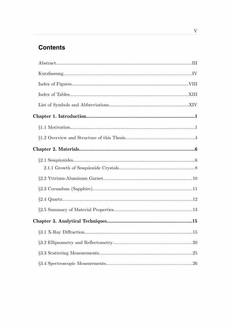
The crystallographic structure of the sesquioxides depends ontemperature, pressure and the cation radius [Hoe66, Rot60]. At thenormal conditions scandia (Sc2O3), yttria (Y2O3), and lutetia (Lu2O3) formthe same cubic C-type bixbyite structure (see figure 2.1). This structure isstable up to the melting point for scandia and lutetia, for yttria it changesto a hexagonal phase slightly below the melting point. The lattice
Materials 7
constants are in the range of10Å1. A unit cell of the bixbyitestructure contains 16 formulaunits (80 atoms). 24 cation sitesof the unit cell have C2-symmetryand 8 cation sites have C3i-symmetry, both six-fold coordi-nated with oxygen. The two-foldaxes of the C2-sites are orientedalong the <100>-direction, thethree-fold axes of the C3i-sitesalong <111>-direction. Chemicalbonds in sesquioxides have ioniccharacter with some part ofcovalent bonding. Due to theidentical crystal structure andrelatively close ionic radii of cations, mixed sesquioxide crystals can alsobe produced. This mixtures, e.g. LuScO3, can be used for tuning of aspecific parameter as, for example, the lattice constant.
Scandia, yttria, and lutetia are insulators with a band gap ofapproximately 6 eV. It means that they are transparent up to theultraviolet region (~200 nm). Detailed investigation can be found in[Abr78, Tom86]. Band structure calculations of yttria have beenperformed by Xu et al. [Xu97]. The conduction band is formed by 4d and5p electron orbitals of Y3+ ions, whereas the valence band is mainlyformed by the 2p orbital of oxygen ions with small contribution ofyttrium 4d and 5p states. Up to now, no investigations of the electronicstructure of scandia or lutetia can be found in the literature.
The fact, that the sesquioxides can be doped with rare-earth elements, istheir most important property for laser applications. The first
1 Here and further in this section the properties of scandia, yttria, ytterbia, andlutetia are discussed in general, see table 2.2 for the values of the specificparameters. The physical and chemical properties are of ytterbia (not given inthe table) are close to that of lutetia.
Figure 2.1: Crystal structure of cubicsesquioxides viewed nearly in <100>-direction. (white – O2-, gray – RE3+(C2),dark gray – RE3+(C3i)).
8 Chapter 2
investigations of spectroscopic and lasing properties of rare-earth-dopedsesquioxides go back up to the late fifties [Bar57, Lev62]. The firstpublished data on the stimulated emission in the Eu3+:Y2O3 can be foundin [Cha63]. The first laser operation of Nd3+:Y2O3 have been demonstratedby Hoskins and Soffer [Hos64]. Thorough investigations of spectroscopicand lasing properties of rare-earth-doped sesquioxides can be found in thetheses of E. Mix [Mix99], L. Fornasiero [For99] and V. Peters [Pet01].
The sesquioxides reveal excellent mechanical and chemical stability. Mohshardness is in the range of 6-7. They are only dissolved in hydrofluoricacid and hot phosphoric acid. Sesquioxides also show quite high thermalconductivity, which even excels that of YAG, which is a widely used laserhost material. This can be favorable for high-power laser applications.Average phonon energy in sesquioxides is quite low for oxide materials,which is especially beneficial for application as a host material for up-conversion lasers in the visible range, since higher phonon energies lead tofaster deexcitation of the excited states.
2.1.1 Growth of Sesquioxide Crystals
Overview of Crystal Growth Techniques
Despite of the fact, that sesquioxides (and especially yttria) are wellinvestigated and some their optical properties are quite favorable for laserapplications, sesquioxide bulk crystals or substrates are not commerciallyavailable up to now. This is mainly caused by their very high meltingtemperature (~2400°C), which hinders the growth of large volume, stressand impurity free single crystals. Up to the end of the nineties noacceptable technique for growth of high quality sesquioxide crystals wereavailable. Most properties of the sesquioxides have been investigated onthe crystals grown by various techniques listed below, but neither of themwas completely acceptable for some reasons (see [Mix99, For99, Pet01] formore detailed discription):
◊ flame-fusion-technique (crystals reveal strong stress, high defectsdensity in the crystalline structure)
Materials 9
◊ scull-melting (crystallization starts from many points, so a largenumber smaller crystals are grown simultaneously)
◊ floating-zone-technique (small volume of grown crystals)
◊ Czochralski- and Nacken-Kyropoulos-method (small volume, due toproblems with the heat abstraction at the high temperatures)
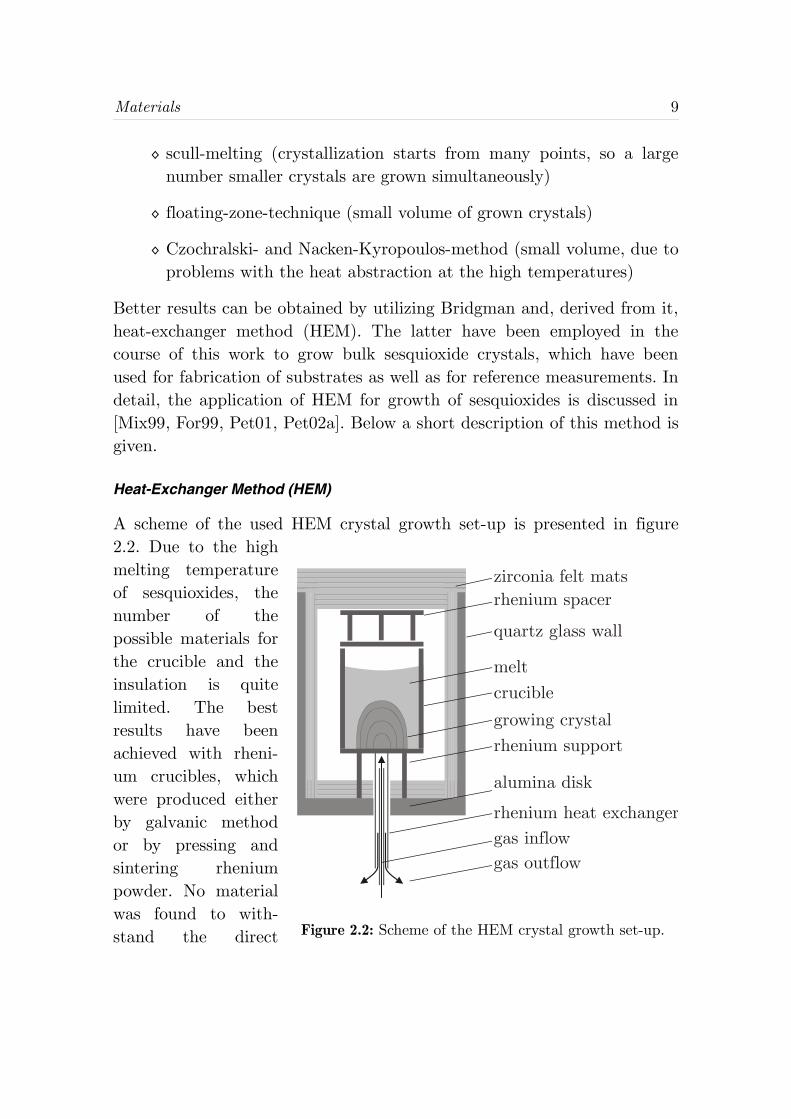
Better results can be obtained by utilizing Bridgman and, derived from it,heat-exchanger method (HEM). The latter have been employed in thecourse of this work to grow bulk sesquioxide crystals, which have beenused for fabrication of substrates as well as for reference measurements. Indetail, the application of HEM for growth of sesquioxides is discussed in[Mix99, For99, Pet01, Pet02a]. Below a short description of this method isgiven.
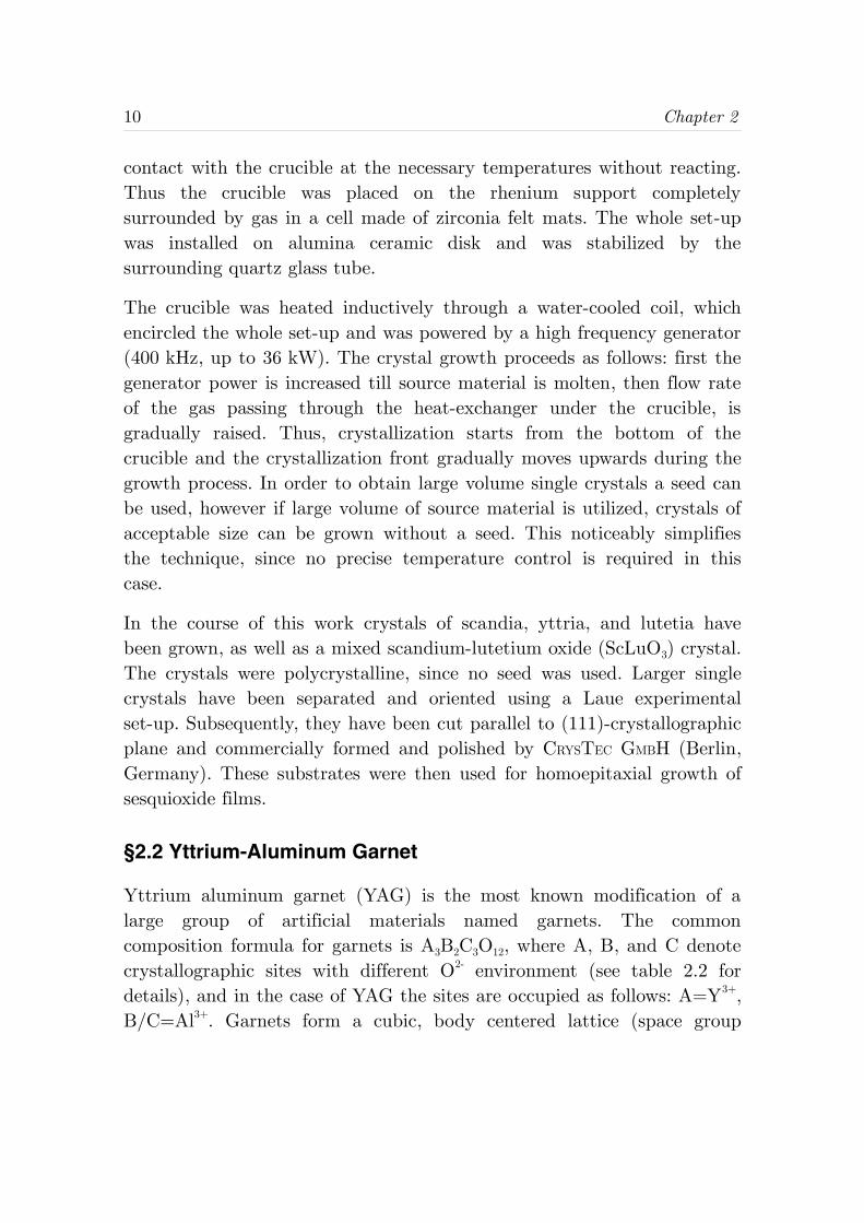
Heat-Exchanger Method (HEM)
A scheme of the used HEM crystal growth set-up is presented in figure2.2. Due to the highmelting temperatureof sesquioxides, thenumber of thepossible materials forthe crucible and theinsulation is quitelimited. The bestresults have beenachieved with rheni-um crucibles, whichwere produced eitherby galvanic methodor by pressing andsintering rheniumpowder. No materialwas found to with-stand the direct Figure 2.2: Scheme of the HEM crystal growth set-up.
zirconia felt mats
quartz glass wall
rhenium spacer
melt
growing crystalrhenium support
rhenium heat exchanger
alumina disk
gas outflowgas inflow
crucible
10 Chapter 2
contact with the crucible at the necessary temperatures without reacting.Thus the crucible was placed on the rhenium support completelysurrounded by gas in a cell made of zirconia felt mats. The whole set-upwas installed on alumina ceramic disk and was stabilized by thesurrounding quartz glass tube.
The crucible was heated inductively through a water-cooled coil, whichencircled the whole set-up and was powered by a high frequency generator(400 kHz, up to 36 kW). The crystal growth proceeds as follows: first thegenerator power is increased till source material is molten, then flow rateof the gas passing through the heat-exchanger under the crucible, isgradually raised. Thus, crystallization starts from the bottom of thecrucible and the crystallization front gradually moves upwards during thegrowth process. In order to obtain large volume single crystals a seed canbe used, however if large volume of source material is utilized, crystals ofacceptable size can be grown without a seed. This noticeably simplifiesthe technique, since no precise temperature control is required in thiscase.
In the course of this work crystals of scandia, yttria, and lutetia havebeen grown, as well as a mixed scandium-lutetium oxide (ScLuO3) crystal.The crystals were polycrystalline, since no seed was used. Larger singlecrystals have been separated and oriented using a Laue experimentalset-up. Subsequently, they have been cut parallel to (111)-crystallographicplane and commercially formed and polished by CRYSTEC GMBH (Berlin,Germany). These substrates were then used for homoepitaxial growth ofsesquioxide films.
§2.2 Yttrium-Aluminum Garnet
Yttrium aluminum garnet (YAG) is the most known modification of alarge group of artificial materials named garnets. The commoncomposition formula for garnets is A3B2C3O12, where A, B, and C denotecrystallographic sites with different O2- environment (see table 2.2 fordetails), and in the case of YAG the sites are occupied as follows: A=Y3+,B/C=Al3+. Garnets form a cubic, body centered lattice (space group
Materials 11
Ia3d). The unit cell of YAG contains eight Y3Al5O12 units. Nowadays,YAG one is of the most important hosts for rare-earth-doped materials as,for example, Nd:YAG or Yb:YAG. Many of commercially produced solid-state lasers are based on this material. Apart from its favorablespectroscopic properties, also its high thermal conductivity, mechanicalstability, and high optical damage threshold stimulated its wideapplication. YAG is an insulator with a band gap of 6.5 eV. Calculationof its electronic structure have been recently performed by Xu and Ching[Xu99, Chi99]. One can also consider YAG as a congruent mixture of twooxides (Y2O3 and Al2O3). Two more congruent compositions of the Y-Al-Osystem exist: YAlO3 (YAP), which forms a perovskite orthorhombiccrystalline lattice and Y4Al2O9 (YAM), having a monoclinic lattice. YAPis also sometimes utilized as a host for rare-earth dopants, but in generalYAP and YAM are less widely used as YAG.
§2.3 Corundum (Sapphire)
Depending on the conditions, aluminum oxide can form several crystallinestructures. The most known is the α-form termed corundum. The matrixitself is colorless, but natural corundum often contains impurities, whichare responsible for its coloration. The red (Cr3+-doped) variation is calledruby and all the other colors – sapphire. However the mineralogical termsapphire is also widely used for pure α-Al2O3 along with the termcorundum.
The unit cell of α-Al2O3 has trigonal symmetry and contains two Al2O3
units. Alternatively the α-Al2O3 lattice can be presented as a hexagonalstructure. The oxygen ions build hexagonal close-packed (hcp) lattice andthe aluminum ions take octahedrally coordinated intersites. α-Al2O3 is aninsulator with a band gap of 9.5 eV. The fundamental absorption edge ishowever overlapped by an absorption of an excitonic state. Also, due toalways present Cr3+-impurities, absorption into a charge-transfer state[Fre90] is observed below the band gap of α-Al2O3. Details on theelectronic structure of corundum can be found in [Xu91].
12 Chapter 2
§2.4 Quartz
Quartz, a form of SiO2, is a very widespread mineral (12% in the Earth'scrust). Pure quartz is fully transparent, whereas natural quartz can havesome coloration due to impurities. From the crystallographic point of viewquartz is an α-form of silica. Depending on temperature and pressure,silica can exist in a large number of other modifications, which includeβ-quartz, tridymite, cristobalite, coesite, stishovite, and keatite. Thus, theα-quartz and the β-quartz should be distinguished. In the framework ofthis theses, where not explicitly noted, the α-form of silica is meant underthe name of quartz.
The unit cell of the α-quartz lattice contains three SiO2 units. The latticehas trigonal symmetry and is acentric, which means that twomodifications (right-hand and left-hand) of the α-quartz crystalline latticeexist. The fact, that quartz is optically active, is explained by thisproperty of the lattice.
When heated over 573°C at atmospheric pressure α-quartz transformsinto β-quartz. The transformation into the β-phase is associated withslight displacements of the ions, without breaking the chemical bonds.The lattice of β-quartz has hexagonal symmetry and is center symmetric.When the temperature is lowered, the transition back into the α-phasetakes place, which is associated with a small but rapid change of thelattice constant and the reduction of the lattice symmetry. This can leadto stress, due to formation of right and left-hand oriented domains. Thedeposition of oxide materials normally requires high substratetemperatures during the deposition (up to 700°C have been used withinthis work). The phase transition back to the α-quartz hinders applicationof quartz as a material for substrates, since the mechanical stress cancause the cracking of the deposited film. Even cracking of the substrateitself have been observed in some cases during this work. Therefore quartzsubstrates have been avoided in the later phase of this work. Morethoroughly the application of quartz substrates for deposition ofsesquioxide PLD-films has been investigated by S. Ehlert in his diplomatheses [Ehl05].
Materials 13
§2.5 Summary of Material Properties
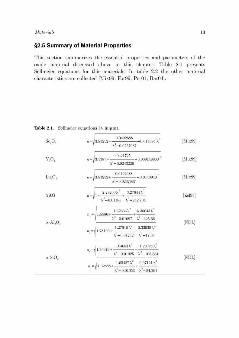
This section summarizes the essential properties and parameters of theoxide material discussed above in this chapter. Table 2.1 presentsSellmeier equations for this materials. In table 2.2 the other materialcharacteristics are collected [Mix99, For99, Pet01, Bär04].
Table 2.1. Sellmeier equations (λ in μm).
Sc2O3 n=3.832520.0492688
λ20.02379870.014094 λ2 [Mix99]
Y2O3 n=3.53870.0421725
20.02432260.009148962 [Mix99]
Lu2O3 n=3.832520.0492688
20.02379870.0140942 [Mix99]
YAG n=12.28200λ2
λ 20.01185
3.27644 λ2
λ2282.734[Zel98]
α-Al2O3
no=1.55861.52365λ2
λ20.01097
5.36043λ 2
λ2325.66
ne=1.781061.27616 λ2
λ20.01242
0.33939λ2
λ217.03
[NDL]
α-SiO2
no=1.309791.04683λ2
λ20.01025
1.20328λ2
λ 2108.584
ne=1.328881.05487λ2
λ 20.01053
0.97121λ2
λ284.261
[NDL]
14 Chapter 2
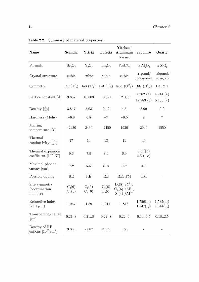
Table 2.2. Summary of material properties.
Name Scandia Yttria LutetiaYttrium-Aluminum
GarnetSapphire Quartz
Formula Sc2O3 Y2O3 Lu2O3 Y3Al5O12 α-Al2O3 α-SiO2
Crystal structure cubic cubic cubic cubic trigonal/hexagonal
trigonal/hexagonal
Symmetry Ia3 (T7h) Ia3 (T7
h) Ia3 (T7h) Ia3d (O10
h) R3c (D53d) P31 2 1
Lattice constant [Å] 9.857 10.603 10.391 12.0034.762 (a)
12.989 (c)
4.914 (a)
5.405 (c)
Density [g
cm3 ] 3.847 5.03 9.42 4.5 3.99 2.2
Hardness (Mohs) ~6.8 6.8 ~7 ~8.5 9 7
Meltingtemperature [°C] ~2430 2430 ~2450 1930 2040 1550
Thermalconductivity [
W
m⋅K] 17 14 13 11 46
Thermal expansioncoefficient [10-6 K-1] 9.6 7.9 8.6 6.9
5.3 ( c)4.5 (⊥c)
Maximal phononenergy [cm-1] 672 597 618 857 950
Possible doping RE RE RE RE, TM TM -
Site symmetry(coordinationnumber)
C2(6)C3i(6)
C2(6)C3i(6)
C2(6)C3i(6)
D2(8) /Y3+,C3i(6) /Al3+,S4(4) /Al3+
Refractive index(at 1 μm) 1.967 1.89 1.911 1.816 1.756(no)
1.747(ne)1.535(no)1.544(ne)
Transparency range[μm]
0.21..8 0.21..8 0.22..8 0.22..6 0.14..6.5 0.18..2.5
Density of RE-cations [1022 cm-3] 3.355 2.687 2.852 1.38 - -
Chapter 3. Analytical Techniques
In this chapter the analytical methods and experimental set-ups employedthroughout this work are described. They include X-ray diffraction,reflectometry and ellipsometry, as well as spectroscopic techniques, suchas emission, excitation, and lifetime measurements.
§3.1 X-Ray Diffraction
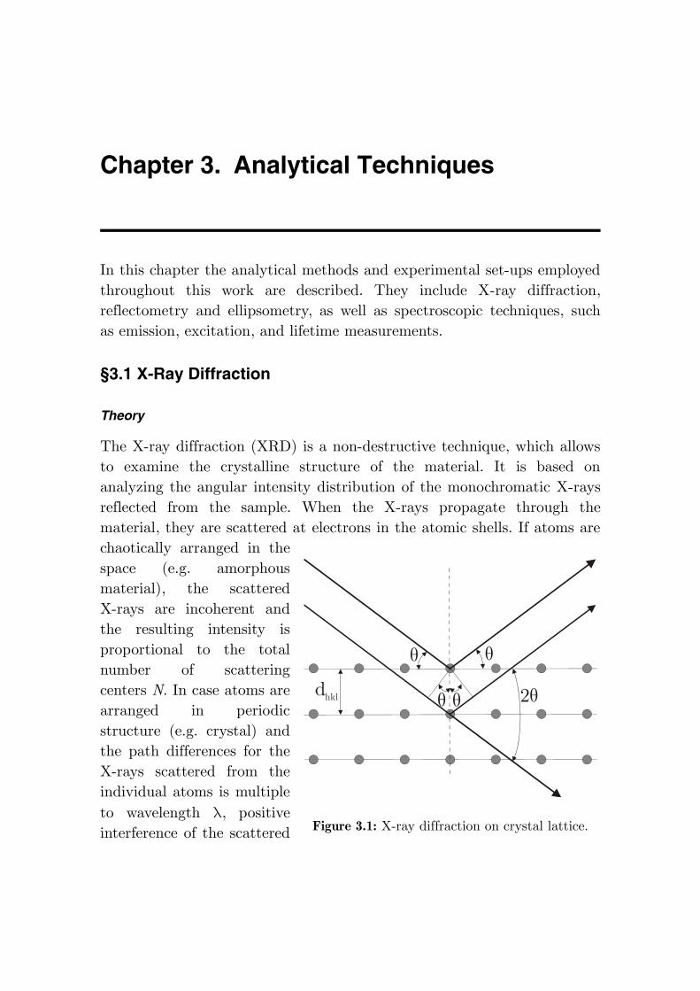
Theory
The X-ray diffraction (XRD) is a non-destructive technique, which allowsto examine the crystalline structure of the material. It is based onanalyzing the angular intensity distribution of the monochromatic X-raysreflected from the sample. When the X-rays propagate through thematerial, they are scattered at electrons in the atomic shells. If atoms arechaotically arranged in thespace (e.g. amorphousmaterial), the scatteredX-rays are incoherent andthe resulting intensity isproportional to the totalnumber of scatteringcenters N. In case atoms arearranged in periodicstructure (e.g. crystal) andthe path differences for theX-rays scattered from theindividual atoms is multipleto wavelength λ, positiveinterference of the scattered Figure 3.1: X-ray diffraction on crystal lattice.
d
θ
θ 2θ
θ
θhkl
16 Chapter 3
X-rays occur (see figure 3.1). In this case the intensity is proportional toN 2. Since N is the number of atoms, which is very large, the effect is verypronounced. Thus, the coherently reflected (diffracted) X-rays are easilydetected in the background of the incoherently scattered X-rays. Theconditions for the positive interference is described by the Braggdiffraction law
2d sin θ =n λ , (3.1)
where λ is the X-rays wavelength, θ is the incidence angle (equal to thereflection angle), as it is defined in figure 3.1, and d is the distancebetween the atomic planes.
For a cubic crystalline lattice, as in the case of sesquioxides or YAG,discussed in this thesis, the interplane distance d can be expressed asfollows
dhkl
=a
h2k 2l 2, (3.2)
a is the lattice constant and h,k,l are Miller indices, which are commonlyused to denote a certainplane or orientation in thecrystalline lattice.
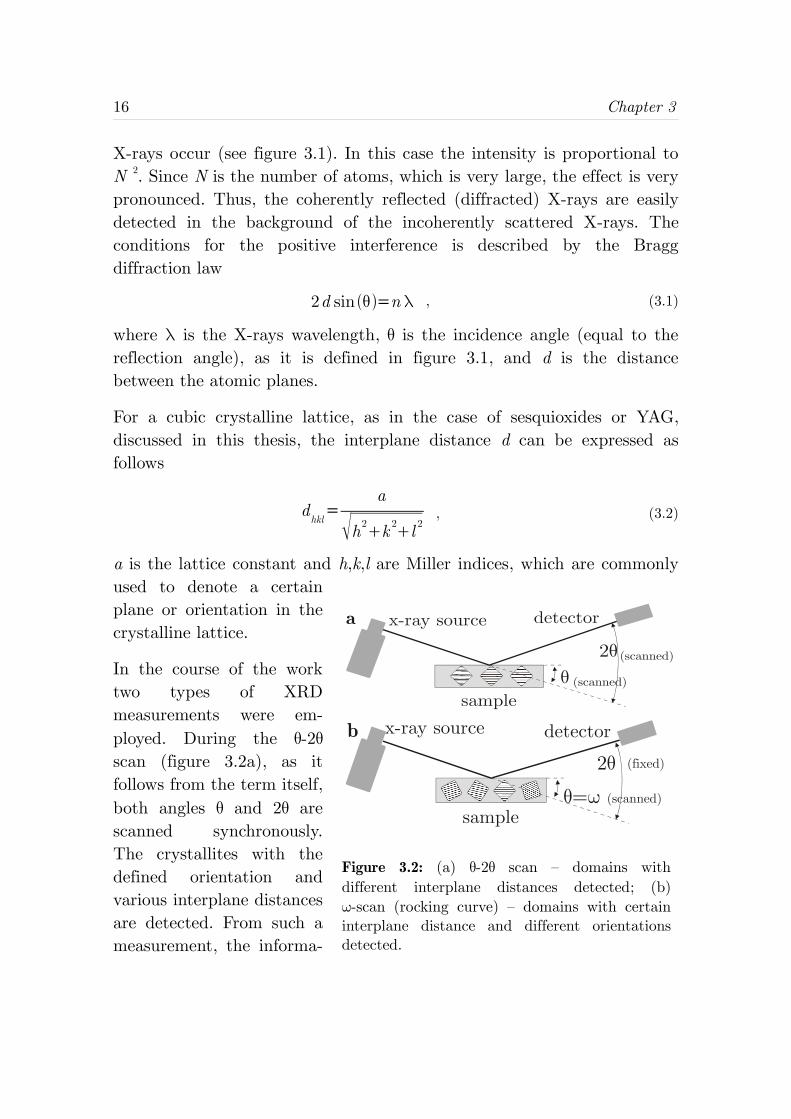
In the course of the worktwo types of XRDmeasurements were em-ployed. During the θ-2θscan (figure 3.2a), as itfollows from the term itself,both angles θ and 2θ arescanned synchronously.The crystallites with thedefined orientation andvarious interplane distancesare detected. From such ameasurement, the informa-
Figure 3.2: (a) θ-2θ scan – domains withdifferent interplane distances detected; (b)ω-scan (rocking curve) – domains with certaininterplane distance and different orientationsdetected.
θ2θ (scanned)
detectorx-ray source
sample(scanned)
a
detectorx-ray source
sampleθ ω=
2θ (fixed)
(scanned)
b
Analytical Techniques 17
tion about the crystalline phase of the material, the size and orientationof crystallites (preferred or random), and the lattice constant is gained.For the rocking-curve measurement (ω-scan), the 2θ angle is kept constantand the θ angle (also termed ω in this case) is scanned (figure 3.2b). It isperformed to investigate the distribution of crystallites orientations.
Whereas from the position of the diffraction peaks, acquired from the θ-2θscan, lattice constants can be determined (equations 3.1 and 3.2), thewidth of the peaks contains information on the dimensions of thecoherently scattering domains in the sample, which are roughly equal tothe size of the crystallites. The relation between the size of the domains(L) and the peaks width (ωpeak=Δ2θ) is given by Scherrer equation [Cul78]
wpeak
=K λ
L cos θ , (3.3)
λ is the X-ray wavelength and K is a factor depending on the form ofcrystallites (K=0.9...1). It should be noted, that this equation is notaccurate and presents only a rough estimation. Assuming the X-ray sourcewith the Cu-Kα1 radiation (λCu-Ka1=1.5404 Å) and K=1, the size ofcrystallite can be estimated using the following simplified equation
L(nm)=
8.827
wpeak
(deg) cos θ . (3.4)
Practically, the intrinsic diffraction peak width (ωpeak) is not equal to themeasured peak width (ωmeas) and is influenced by the finite instrumentalresolution of the diffractometer (ωinst). In case the diffraction peaks andinstrumental broadening have Gaussian profile, the intrinsic peak widthcan be determined by
wpeak
=wmeas
2w
inst
2 . (3.5)
Actually, the diffraction lines have a form close to that described by aPseudo-Voigt function, which is the mixture of Gaussian and Lorentzianprofiles. However, in practice it was found that the line profiles do notdeviate substantially from the Gaussian form. Thus, in this approximationequation 3.7 was used to estimate the intrinsic peak.
18 Chapter 3
Experimental
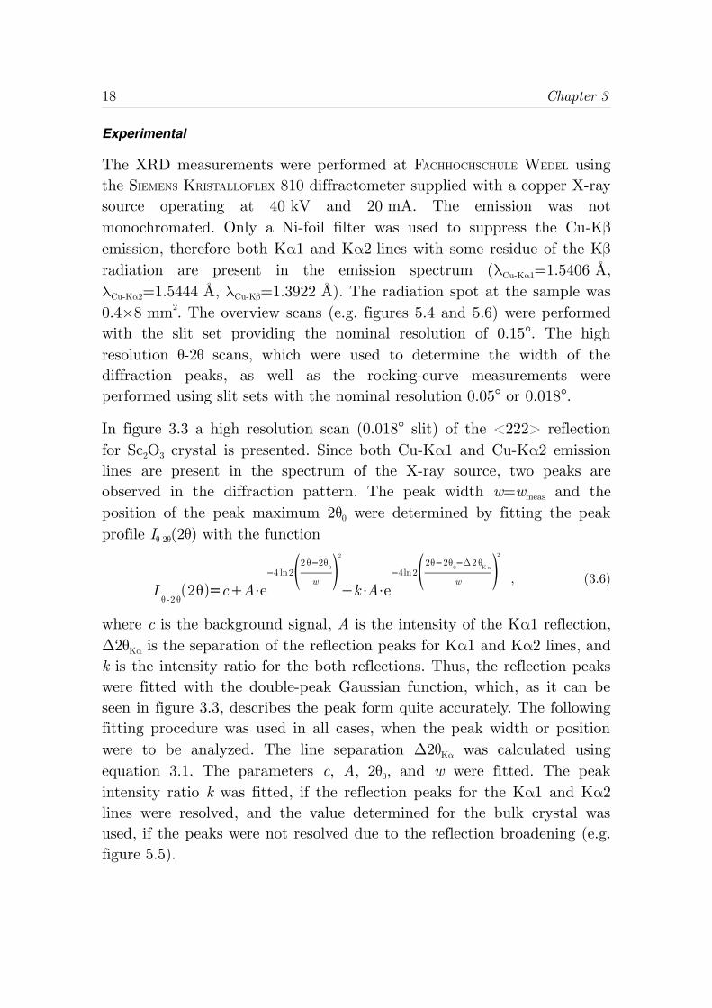
The XRD measurements were performed at FACHHOCHSCHULE WEDEL usingthe SIEMENS KRISTALLOFLEX 810 diffractometer supplied with a copper X-raysource operating at 40 kV and 20 mA. The emission was notmonochromated. Only a Ni-foil filter was used to suppress the Cu-Kβemission, therefore both Kα1 and Kα2 lines with some residue of the Kβradiation are present in the emission spectrum (λCu-Kα1=1.5406 Å,λCu-Kα2=1.5444 Å, λCu-Kβ=1.3922 Å). The radiation spot at the sample was0.4×8 mm2. The overview scans (e.g. figures 5.4 and 5.6) were performedwith the slit set providing the nominal resolution of 0.15°. The highresolution θ-2θ scans, which were used to determine the width of thediffraction peaks, as well as the rocking-curve measurements wereperformed using slit sets with the nominal resolution 0.05° or 0.018°.
In figure 3.3 a high resolution scan (0.018° slit) of the <222> reflectionfor Sc2O3 crystal is presented. Since both Cu-Kα1 and Cu-Kα2 emissionlines are present in the spectrum of the X-ray source, two peaks areobserved in the diffraction pattern. The peak width w=wmeas and theposition of the peak maximum 2θ0 were determined by fitting the peakprofile Iθ-2θ(2θ) with the function
Iθ -2 θ
2θ =cA⋅e4 ln22 θ2θ
0
w 2
k⋅A⋅e4ln22θ2θ
0Δ2 θ
Kα
w 2
, (3.6)
where c is the background signal, A is the intensity of the Kα1 reflection,Δ2θKα is the separation of the reflection peaks for Kα1 and Kα2 lines, andk is the intensity ratio for the both reflections. Thus, the reflection peakswere fitted with the double-peak Gaussian function, which, as it can beseen in figure 3.3, describes the peak form quite accurately. The followingfitting procedure was used in all cases, when the peak width or positionwere to be analyzed. The line separation Δ2θKα was calculated usingequation 3.1. The parameters c, A, 2θ0, and w were fitted. The peakintensity ratio k was fitted, if the reflection peaks for the Kα1 and Kα2lines were resolved, and the value determined for the bulk crystal wasused, if the peaks were not resolved due to the reflection broadening (e.g.figure 5.5).
Analytical Techniques 19
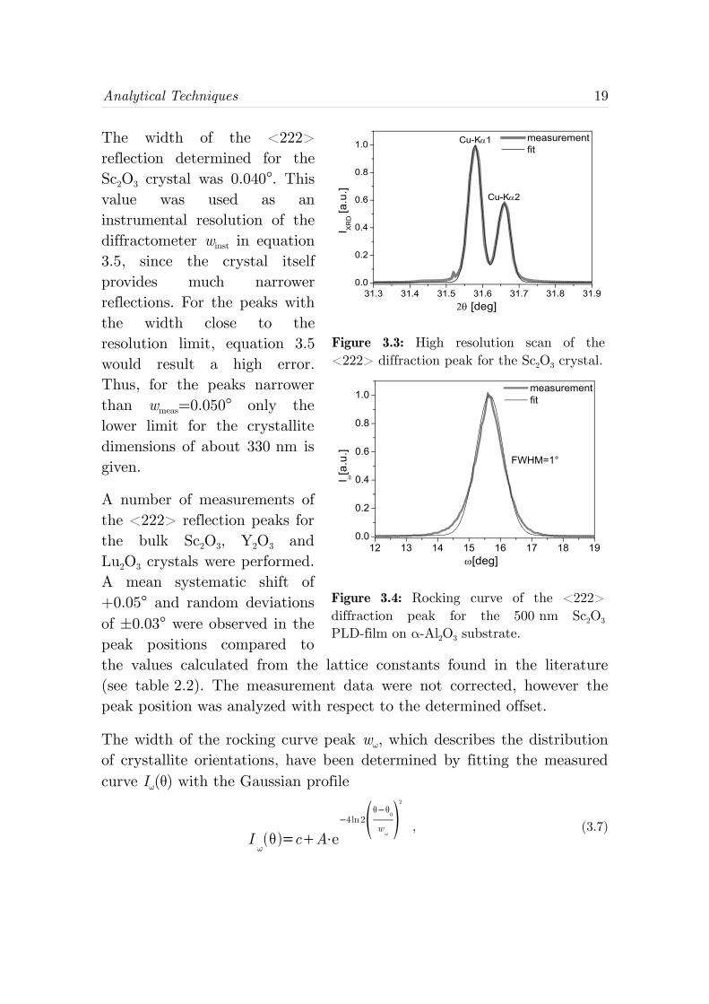
The width of the <222>reflection determined for theSc2O3 crystal was 0.040°. Thisvalue was used as aninstrumental resolution of thediffractometer winst in equation3.5, since the crystal itselfprovides much narrowerreflections. For the peaks withthe width close to theresolution limit, equation 3.5would result a high error.Thus, for the peaks narrowerthan wmeas=0.050° only thelower limit for the crystallitedimensions of about 330 nm isgiven.
A number of measurements ofthe <222> reflection peaks forthe bulk Sc2O3, Y2O3 andLu2O3 crystals were performed.A mean systematic shift of+0.05° and random deviationsof ±0.03° were observed in thepeak positions compared tothe values calculated from the lattice constants found in the literature(see table 2.2). The measurement data were not corrected, however thepeak position was analyzed with respect to the determined offset.
The width of the rocking curve peak wω, which describes the distributionof crystallite orientations, have been determined by fitting the measuredcurve Iω(θ) with the Gaussian profile
Iωθ =cA⋅e
4ln2θθ0
w ω 2
, (3.7)
Figure 3.4: Rocking curve of the <222>diffraction peak for the 500 nm Sc2O3
PLD-film on α-Al2O3 substrate.
12 13 14 15 16 17 18 190.0
0.2
0.4
0.6
0.8
1.0
I ω[a
.u.]
ω[deg]
measurement fit
FWHM=1°
Figure 3.3: High resolution scan of the<222> diffraction peak for the Sc2O3 crystal.
31.3 31.4 31.5 31.6 31.7 31.8 31.90.0
0.2
0.4
0.6
0.8
1.0
Cu-Kα2
measurement fit
I XR
D [a
.u.]
2θ [deg]
Cu-Kα1
20 Chapter 3
where c is the background, A is the peak amplitude, and θ0 is the positionof the peak maximum. The measured rocking curve and the fittingfunction profile for the 500 nm Sc2O3 deposited on the sapphire substrateis presented in figure 3.4 as an example. For the narrow peaks the widthabout 1° and below the form of the ω-scans deviated slightly from theGaussian profile, as it can be seen in the figure. For consistency, fittingwith equation 3.7 was used also in these cases as well.
§3.2 Ellipsometry and Reflectometry
Both ellipsometry and reflectometry are based on the analysis of lightreflected from the sample surface. The measurements are non-destructiveand can be performed remotely. Thus, they can be employed in thesituations, where application of other techniques might be problematic,as, for example, in a vacuum chamber during the deposition process.
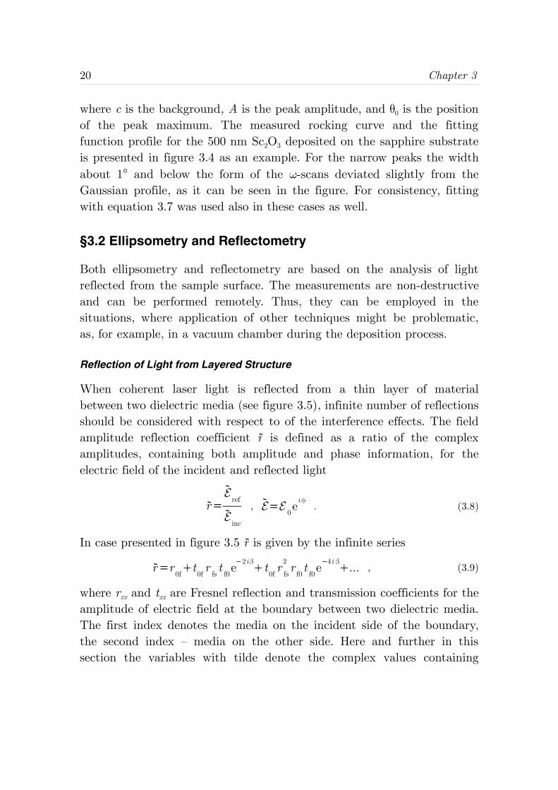
Reflection of Light from Layered Structure
When coherent laser light is reflected from a thin layer of materialbetween two dielectric media (see figure 3.5), infinite number of reflectionsshould be considered with respect to of the interference effects. The fieldamplitude reflection coefficient r is defined as a ratio of the complexamplitudes, containing both amplitude and phase information, for theelectric field of the incident and reflected light
r =E
ref
Einc
, E=E0ei φ
. (3.8)
In case presented in figure 3.5 r is given by the infinite series
r =r0f
t0fr
fst
f0e2i β
t0fr
fs
2 rf0t
f0e4i β
... , (3.9)
where rxx and txx are Fresnel reflection and transmission coefficients for theamplitude of electric field at the boundary between two dielectric media.The first index denotes the media on the incident side of the boundary,the second index – media on the other side. Here and further in thissection the variables with tilde denote the complex values containing
Analytical Techniques 21
phase information in addition tothe amplitude. The expressions forthe Fresnel coefficients arepolarization dependent and can befound in appendix B. The phaseshift β between the light reflecteddirectly from the front surface ofthe film and the light reflectedfrom the film-substrate boundaryis given by
β=2n
fd
f
λcos θ
f , (3.10)
where nf is the refractive index of the film material, df is the filmthickness, λ is the wavelength of the light, and θf is the light incidenceangle inside of the film.
Equation 3.9 can be also adapted for the more complicated case, whenmore than one layer is present. In case a single layer between two half-infinite media (film on substrate) is considered, the infinite series of themultiple reflections presented by equation 3.9 converges into
rσ ,π=r
0f
σ ,πr
fs
σ ,πe2i β
1r0f
σ ,πrfs
σ ,πe2 i β. (3.11)
σ and π denote two versions of the equation for the σ- and and π-polarizations, respectively.
In the case of reflectometry the intensity of the reflected light ismeasured. Thus, only the intensity reflection coefficient, which containsno phase information, is determined. Using equation 3.11 the intensityreflection coefficient can be presented as
Rσ ,π=∣ r σ, π∣2=r
0f
σ ,π2r
fs
σ ,π22r
0f
σ ,πrfs
σ ,πcos 2β
1r0f
σ,π2rfs
σ ,π22r0f
σ , πrfs
σ ,πcos 2β. (3.12)
Figure 3.5: Reflection of light fromlayered structure.
θ0
θf
θf
θs
n0
nf
ns
22 Chapter 3
The intensity measurements have not very high accuracy and containlittle information, therefore single reflection coefficient measurements arealmost not used. Typically, the reflection (or transmission) of the sampleis measured over a certain wavelength region, so that the measured curvecan be fitted with a calculated one. This helps to obtain more precisevalues for the thickness or refractive index of the film.
Another possibility is to monitor the reflection coefficient continuouslyduring the deposition of the film. In the framework of this thesis thereflectometry was employed to control the thickness of the deposited filmsin situ. The absolute intensity can be disregarded in this case, since theform of the signal gives enough information to determine the thickness, ifthe reflective indices are known. The experimental implementation of themethod and the data analysis are discussed below in section 4.2.
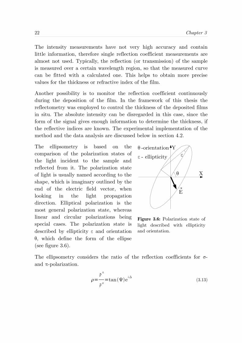
The ellipsometry is based on thecomparison of the polarization states ofthe light incident to the sample andreflected from it. The polarization stateof light is usually named according to theshape, which is imaginary outlined by theend of the electric field vector, whenlooking in the light propagationdirection. Elliptical polarization is themost general polarization state, whereaslinear and circular polarizations beingspecial cases. The polarization state isdescribed by ellipticity ε and orientationθ, which define the form of the ellipse(see figure 3.6).
The ellipsometry considers the ratio of the reflection coefficients for σ-and π-polarization.
=rπ
r σ=tan ΨeiΔ
(3.13)
Figure 3.6: Polarization state oflight described with ellipticityand orientation.
E
ε
θ
Y
X
θ -orientation
ε - ellipticity
Analytical Techniques 23
This complex ratio is usually expressed through two real quantities Ψ andΔ, which are determined by solving the matrix equation
1
Χdet
=[1 0
1 tan ΨeiΔ] 1
Χsour
,(3.14)
where Χdet,sour are expressed through experimentally measured θdet,sour andεdet,sour
Χdet,sour
=tan θ
det,souri tan ε
det,sour
1i tan θdet,sour
tan εdet,sour
. (3.15)
Thus, oppositely to the reflectometry, where the ratio of intensities isdetermined, the ellipsometry is intrinsically more precise technique, sincethe experimentally determined angles ε and θ can be measured withhigher accuracy than intensity. This makes the ellipsometry a much moresensitive technique. The ellipsometric measurement also maintains thephase value, therefore more information about the sample is gained insuch a measurement. The wavelength dependent measurements can beperformed to determine the dispersion of the material.
Ellipsometry (Experimental)
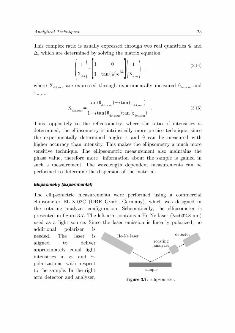
The ellipsometric measurements were performed using a commercialellipsometer EL X-02C (DRE GMBH, Germany), which was designed inthe rotating analyzer configuration. Schematically, the ellipsometer ispresented in figure 3.7. The left arm contains a He-Ne laser (λ=632.8 nm)used as a light source. Since the laser emission is linearly polarized, noadditional polarizer isneeded. The laser isaligned to deliverapproximately equal lightintensities in σ- and π-polarizations with respectto the sample. In the rightarm detector and analyzer, Figure 3.7: Ellipsometer.
detector
rotatinganalyzer
sample
He-Ne laser
24 Chapter 3
rotated with a high-precision step motor (specified accuracy of 0.002°),are located.
Manually adjusting the position of both arms, the measurements can beperformed at different light incidence angles. The reference measurementof the light source is performed, when the arms are set horizontally, sothat the laser beam directly meets detector. The ellipsometer wascontrolled by a computer and data was acquired and analyzed with thesupplied software.
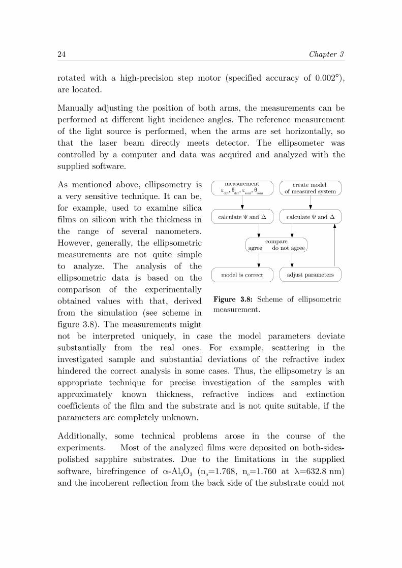
As mentioned above, ellipsometry isa very sensitive technique. It can be,for example, used to examine silicafilms on silicon with the thickness inthe range of several nanometers.However, generally, the ellipsometricmeasurements are not quite simpleto analyze. The analysis of theellipsometric data is based on thecomparison of the experimentallyobtained values with that, derivedfrom the simulation (see scheme infigure 3.8). The measurements mightnot be interpreted uniquely, in case the model parameters deviatesubstantially from the real ones. For example, scattering in theinvestigated sample and substantial deviations of the refractive indexhindered the correct analysis in some cases. Thus, the ellipsometry is anappropriate technique for precise investigation of the samples withapproximately known thickness, refractive indices and extinctioncoefficients of the film and the substrate and is not quite suitable, if theparameters are completely unknown.
Additionally, some technical problems arose in the course of theexperiments. Most of the analyzed films were deposited on both-sides-polished sapphire substrates. Due to the limitations in the suppliedsoftware, birefringence of α-Al2O3 (no=1.768, ne=1.760 at λ=632.8 nm)and the incoherent reflection from the back side of the substrate could not
Figure 3.8: Scheme of ellipsometricmeasurement.
create model of measured system
calculate Ψ and Δ
compareagree do not agree
adjust parametersmodel is correct
calculate Ψ and Δ
measurementε
det, θ
det, ε
sour, θ
sour
Analytical Techniques 25
be included into the simulation. A refractive index matching gel (n=1.780at λ=589.3 nm) and another sapphire substrate with the dispersive backside was used to suppress the undesired reflection. However, thebirefringence and the residual reflection still might influence the accuracyof the measurements. Therefore the results obtained from thesemeasurements were only used to compare the properties of the films. Theabsolute values of the determined refractive indices should be treated withcare.
§3.3 Scattering Measurements
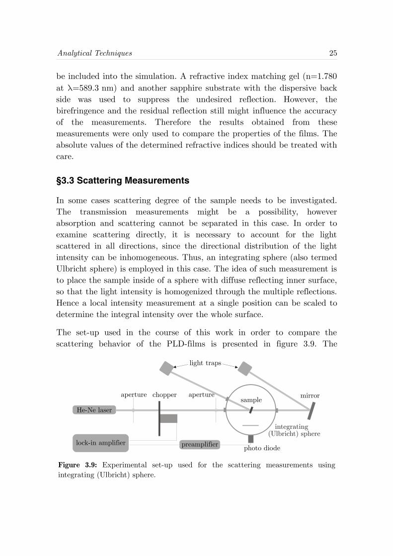
In some cases scattering degree of the sample needs to be investigated.The transmission measurements might be a possibility, howeverabsorption and scattering cannot be separated in this case. In order toexamine scattering directly, it is necessary to account for the lightscattered in all directions, since the directional distribution of the lightintensity can be inhomogeneous. Thus, an integrating sphere (also termedUlbricht sphere) is employed in this case. The idea of such measurement isto place the sample inside of a sphere with diffuse reflecting inner surface,so that the light intensity is homogenized through the multiple reflections.Hence a local intensity measurement at a single position can be scaled todetermine the integral intensity over the whole surface.
The set-up used in the course of this work in order to compare thescattering behavior of the PLD-films is presented in figure 3.9. The
Figure 3.9: Experimental set-up used for the scattering measurements usingintegrating (Ulbricht) sphere.
lock-in amplifier
He-Ne laser
chopper
light traps
aperture aperture mirror
photo diode
sample
integrating (Ulbricht) sphere
preamplifier
26 Chapter 3
samples were placed in the middle of the sphere with the diameter of15 cm, which inner surface was covered with the BaSO4 based paintreflecting about 98% of light at the wavelength of the He-Ne laser(632.8 nm) used as the light source. An entrance opening with thediameter of 6 mm, as well as two 8 mm windows for the transmitted andreflected light were provided. A Si-detector with the area of 7 mm2 isbuild-in into the sphere wall. A barrier in front of the detector blocked thelight coming directly from the sample, thus only the averaged lightintensity was detected. Since the lock-in detection technique have beenused, the environment light did not influence the measurementsnoticeably. However, the light traps were required for the reflected andtransmitted laser beams, so that the light was not scattered back into thesphere. Also two apertures were placed along the beam path to block thefluorescence emission and scattered light coming out of the He-Ne laser.
It have been found, that the measurements are strongly influenced bydust and pollution on sample surface. Thus, the experiments using theintegrating sphere were performed before all other investigations. Thesamples were thoroughly cleaned with pressed air. Up to tenmeasurements have been performed for each sample at different positions,then strongly deviating values were discarded and a mean value wascalculated.
§3.4 Spectroscopic Measurements
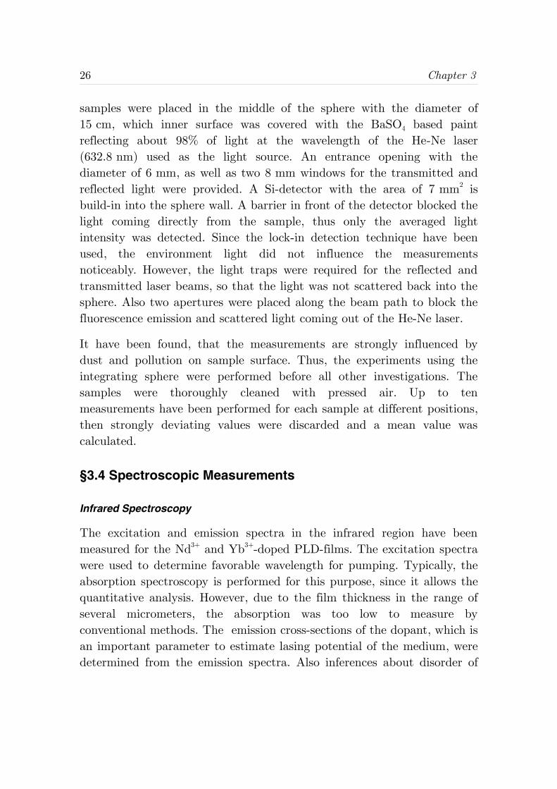
Infrared Spectroscopy
The excitation and emission spectra in the infrared region have beenmeasured for the Nd3+ and Yb3+-doped PLD-films. The excitation spectrawere used to determine favorable wavelength for pumping. Typically, theabsorption spectroscopy is performed for this purpose, since it allows thequantitative analysis. However, due to the film thickness in the range ofseveral micrometers, the absorption was too low to measure byconventional methods. The emission cross-sections of the dopant, which isan important parameter to estimate lasing potential of the medium, weredetermined from the emission spectra. Also inferences about disorder of
Analytical Techniques 27
the crystalline structure of the PLD-film can be made from the inhomoge-neous broadening of the dopant spectra.
The measurements have been performed using the set-up presented infigure 3.10. The continuous emission of the Ti:Sapphire laser was used forexcitation. Two sets of resonator mirrors allowed operation either in700 nm – 850 nm or in 850 nm – 1000 nm ranges. The emission has beendetected by a InGaAs photo diode. The measurements have beenperformed at room temperature. The excitation spectra were corrected forthe wavelength dependency of the output of Ti:Sapphire laser. Using theemission spectrum of a tungstate lamp at the temperature of 2600 K andthe calculated intensity distribution of the black-body (Planck's law), thespectral response function of the set-up was calculated to calibrate theemission spectra.
The emission cross-section spectra σem(λ) for the transition between twomultiplets i and j of the RE-ion were calculated from measured emissionspectra I(λ) using the Füchtbauer-Ladenburg equation [Aul82, Pay92]
σem =β
i jλ5I λ
8πn2c τrad ∫λ⋅I λ d λ
. (3.16)
Figure 3.10: Scheme of experimental set-up for the spectroscopic measurements innear- infrared region.
sampleSPEX 1000Mmonochromator
computer
chopper
detector
Nd:YVO laser ( ) cw=512 nm (2 ) λ ω
Ti:Sapphire laser λ=700-1000 nm (cw)
grating 600 lines/mm
lock-in amplifier
28 Chapter 3
τrad is the radiative lifetime of the excited state i of the dopant, n is therefractive index of the medium, c is the speed of light in free space, andβi→j is the normalized probability of the radiative transition from theexcited state i into the lower state j, termed as a branching ratiocoefficient.
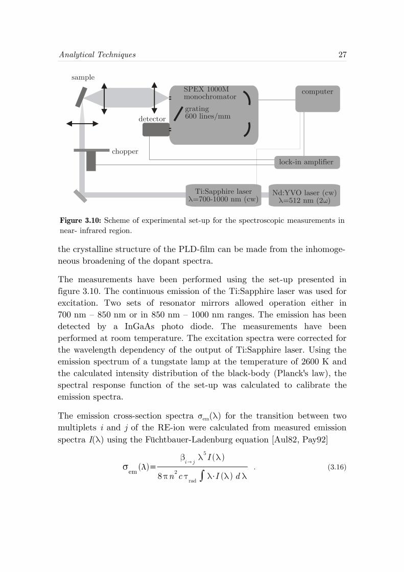
Spectroscopy in Visible Region (Fluorolog)
The emission and excitationspectra for the Eu-dopedPLD-films were measuredusing the modularspectrometer FL321FLUOROLOG-3 (JOBIN YVON).The monochromated light ofthe high-pressure Xenonlamp was used forexcitation. The emission wasdetected by the R928(HAMAMATSU) photomulti-plier, cooled down to -15°Cto reduce electronic noise.The emission spectra were corrected with the known spectral response ofthe emission channel. The intensity of the excitation light, measured by areference photo diode with known sensitivity, was used for correction ofexcitation measurements. The set-up was fully computer controlled. Thesecond emission channel with the CCD detector was not employed in theframework of this thesis.
Time Resolved Emission Measurements
The time resolved emission measurements were used to determine thelifetimes of the excited states of Nd3+ and Yb3+-dopants. This data wasused to evaluate the quality of the crystalline lattice of PLD-film, sincelattice defects and local symmetry distortion can substantially reduce thelifetimes. The excited state lifetimes are also an important parameters toestimate the possibility of laser operation in the medium.
Figure 3.11: Scheme of Fluorolog spectrometerset-up.
emissionmonochromator
#1
emissionmonochromator
#2
photo-diode
samplephoto-multiplier
computerXe-lamp
excitationmonochromator
CCD
filter
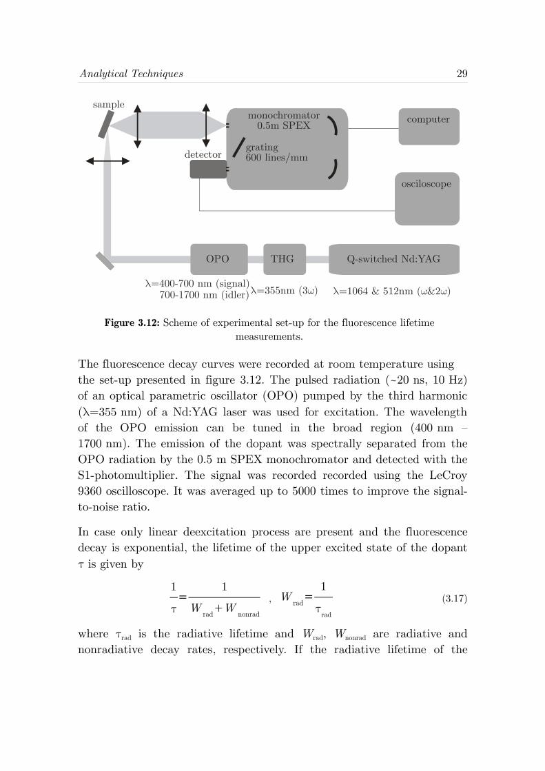
Analytical Techniques 29
The fluorescence decay curves were recorded at room temperature usingthe set-up presented in figure 3.12. The pulsed radiation (~20 ns, 10 Hz)of an optical parametric oscillator (OPO) pumped by the third harmonic(λ=355 nm) of a Nd:YAG laser was used for excitation. The wavelengthof the OPO emission can be tuned in the broad region (400 nm –1700 nm). The emission of the dopant was spectrally separated from theOPO radiation by the 0.5 m SPEX monochromator and detected with theS1-photomultiplier. The signal was recorded recorded using the LeCroy9360 oscilloscope. It was averaged up to 5000 times to improve the signal-to-noise ratio.
In case only linear deexcitation process are present and the fluorescencedecay is exponential, the lifetime of the upper excited state of the dopantτ is given by
1
τ=
1
Wrad
Wnonrad
, Wrad
=1
τrad
(3.17)
where τrad is the radiative lifetime and Wrad, Wnonrad are radiative andnonradiative decay rates, respectively. If the radiative lifetime of the
Figure 3.12: Scheme of experimental set-up for the fluorescence lifetimemeasurements.
samplemonochromator
0.5m SPEX computer
osciloscope
detector
λ=1064 & 512nm ( &2 )ω ω
THGOPO
λ=355nm (3 )ωλ=400-700 nm (signal)
700-1700 nm (idler)
grating 600 lines/mm
Q-switched Nd:YAG
30 Chapter 3
excited state is known, the quantum efficiency of the emission ηq can beestimated
ηq=
Wrad
Wrad
Wnonrad
=τ
τrad
. (3.18)
The quantum efficiency of the active material influences the performanceof laser operation and amount of the produced heat. Thus, high quantumefficiency is desired, especially for the material used as an active mediumin the high power lasers.
SuperLumi Experimental Set-up
Some emission measurements were performed at the SUPERLUMI station(DESY, Hamburg, Germany), which is mainly designed for thespectroscopic investigations in the UV region. The excitation source issynchrotron radiation from the positron storage ring DORIS, whichspectrally is filtered by the primary monochromator. The radiation in therange 60 nm – 330 nm with the resolution of 0.3 nm is available forexperiments. Since the radiation in the wavelength region below 200 nm isstrongly absorbed by any material (including air), no window could beplaced to separate the set-up from the synchrotron ring. Thus the samplechamber, the primary monochromator, and the light channels areconstantly maintained under ultra-high vacuum conditions. The sampleswere placed on a copper bar, which could be cooled with liquid heliumdown to 10 K. The emission was analyzed using a secondarymonochromator and a cooled (-114°C) CCD-camera. A more detaileddescription of the set-up can be found in [Neg03, Möl86]. Combination ofintense radiation source, sensitive detector, and possibility to work at lowtemperatures allowed to detected emission for the Yb2O3 PLD-films,which could not been observed using other set-ups.
Chapter 4. Film Preparation by Pulsed
Laser Deposition
First section of this chapter gives an overview on different depositiontechniques, that can be used to produce doped and undoped oxide filmsfor optical applications. Also waveguide fabrication techniques not basedon deposition methods are mentioned. Practical aspect of pulsed laserdeposition and film preparation is discussed in more detail in the secondpart of the chapter. Analysis of scandia film properties and optimaldeposition parameter is presented in the last section.
§4.1 Deposition Techniques
4.1.1 Overview
Film fabrication methods can be classified into several categoriesdepending on the phase of material, which is deposited on substrate. Alsoa separate group of waveguide fabrication methods, based on modificationof substrate material, can be distinguished:
◊ solid
• direct or thermal bonding
◊ liquid
• liquid phase epitaxy (LPE)
• sol-gel process
◊ gas or plasma
• chemical vapor deposition (CVD)
• molecular beam epitaxy (MBE)
32 Chapter 4
• pulsed laser deposition (PLD)
• sputtering
• thermal evaporation (resistive heating, EBV, IAD)
◊ modification of material
• indiffusion
• ion exchange
• ion implantation
• direct laser writing
Below short descriptions of the techniques are given.
Bonding
Bonding in based on the attraction due to Van der Waals forces, whichappear, if two very smooth surfaces are attaches together closely(hundreds of nanometers). Both substrate and active material are usuallypolished with epitaxial quality and attached together. Sometimesadditional pressure or heating is applied to enhance bonding strength.After that the structure is quite stable, so that the active layer can bepolished down to the necessary thickness or finishing of the end faces canbe done. If necessary a cladding layer can be attached on top.
Due to the fact that bulk material is used and all surfaces perfectlypolished, bonding seems to be a suitable technique to produce highquality and low loss waveguides. High-power laser operation have beendemonstrated in a bonded waveguide structure [Mac01]. However, thetechnique is time consuming and it might be complicated to producewaveguides thiner than some tens of micrometers.
Liquid Phase Epitaxy (LPE)
To produce a LPE-film a suitable substrate is immersed in aoversaturated melt or solution of material, it precipitates onto thesubstrate and a film is formed. The solution in low temperature meltingsubstances (flux) is often used to reduce the process temperature. LPE isquite simple and scalable technique, since multiple substrates can be used
Film Preparation by Pulsed Laser Deposition 33
simultaneously. It was widely used for growth of semiconductor materials,but also active oxide materials for laser applications can be grown. Forexample Nd:YAG waveguide laser grown by LPE was demonstrated[Cha92], also Yb:YAG LPE-films have been used as active medium for athin disk laser [Ubi04]. The method provides quite low degree of filmthickness control, therefore fabrication of thin films can be complicated.Another disadvantage of the technique is the necessity to find a suitableflux material. In some cases contamination of the film with flux materialand cracking of grown films can occur.
Sol-Gel Process
Sol is a colloidal suspension of solid particles in liquid, which is producedby hydrolysis of metalorganic compounds (precursors) and subsequentwater condensation. This particles with the size from some nanometers toa few hundreds nanometers are precipitated from solution onto asubstrate either by dipping it into suspension or by spinning. At thisstage colloidal particles condensed on the substrate form gel. After dryingat room temperature or with some heating a xerogel film is formed.Afterwards, annealing at higher temperatures can be used to improvedensity and crystallinity of the film, so that ceramic- or glass-like film isproduced. The advantage of the process is its simplicity, since no specialequipments is required and the whole process can be carried out atrelatively low temperatures (<100°C). Thus, temperature sensitivecompounds can be incorporated into the film. However, in order toproduce high quality films, proper precursors and process parameter needto be found, which is not always trivial. Also stress and cracking of filmscan be a issue.
Chemical Vapor Deposition (CVD)
In case of chemical vapor deposition source material for the filmfabrication is a gaseous compound (precursor), containing the ionsintended for the film formation. Decomposition of the molecules iscatalyzed at the surface of the heated substrate. Rests of the compoundare desorbed from the substrate and removed. Thus, in order to depositfilms of certain material, first a suitable precursor is to be found.
34 Chapter 4
Contamination of the chamber and usage of reactive materials asprecursors might result some difficulties for use of this technique in anexperimental environment.
Molecular Beam Epitaxy (MBE)
The idea of MBE is to deposit every single substance of the multicomponent film separately. Every component is placed into an effusioncell, which is isothermally heated to evaporate the material. Through anaperture in the cell wall evaporated substance is expanding towards asubstrate forming a molecular beam. Intensity of each beam and thusdeposition of individual components can be controlled very precisely.Uultra high vacuum (~10-10 mbar) is a necessary condition for the MBEprocess. High substrate temperatures are also required to produce highquality films, due to the thermal character of the deposition process.
Very high quality, epitaxial films can be produced by MBE. However, dueto vacuum requirements, this technique is quite expensive and inflexible.Thus, MBE is typically employed to fabricate semiconductor films, wherefilm quality is a critical factor. MBE scandia films have been reportedrecently [Kle05].
Thermal Evaporation
A resistive heating or electron beam evaporation (EBV) can be used tomelt and evaporate source material, which is then deposited onsubstrates. Since typical particles energy is less 1 eV, typicallyamorphous, not quite dense films are produced. Substrates are usuallyheated, in order to improve the density of the films. An ion beamassistance can also be employed. In this case the technique is typicallyreferred to as ion-assisted deposition (IAD). The thermal evaporationtechniques are often used to fabricate optical coatings. However, thismethods are not suitable for deposition of high quality crystalline films.Also deposition of complex materials is an issue, since different vaporpressures of the components can result in different deposition rates, thusthe stoichiometry is often not preserved.
Film Preparation by Pulsed Laser Deposition 35
Sputtering
Sputtering effect can be achieved by acceleration of inert gas ions, whichbombard the target and mechanically eject the material. DC acceleration(in kV range) is used to sputter conductive material. In order to avoidcharging effects, RF sputtering is utilized for deposition of insulators.Sputtering is distinguished by high deposition rates and broad angulardistribution of the plume, which allows large area depositions. Along withthe thermal evaporation, this method is often used to fabricate opticalcoatings. Crystalline film growth can be achieved, if substrate is heated.Additional voltage can be applied to accelerate the particles in the plume,which typically have energies in the range 0.1-1 eV. A disadvantage of thetechnique for experimental applications is a large amount of material,which is necessary for the target.
Indiffusion and Ion Exchange
Indiffusion is a waveguide fabrication technique based on increase ofrefractive index of material, when appropriate ions are incorporated intoit. First material, that is to be incorporated, is deposited onto thesubstrate, which is then placed into oven at high temperature (>1000°C)for some period of time for diffusion to occur. Ion exchange method isbased on similar principle. The substrate is placed in the bath ofappropriate molten material, so that the ions from the substrate and fromthe melt exchange slowly.
Thus, a layer of modified material is produced. In case of correct materialchoice, the layer will have higher refractive index and can be used as awaveguide. Masking can be employed in both methods to producechannels or other structures. Since crystalline material is taken as asource, high quality of layers can be expected. For example Ti:sapphirewaveguide laser have been realized by indiffusion [Hic98]. However longprocessing times, which can be up to several days long, and incapabilityto produce sharp, well defined structures are major disadvantages of bothtechniques.
36 Chapter 4
Ion Implantation and Direct Laser Writing
Modification of material can be achieved by bombarding it with highenergy ions in the range of MeV. At high energies ions do not affect thecrystalline lattice, and material is destroyed only when they aredecelerated. Thus, the effect can be produced in the underlying materialand buried structures can be fabricated. Material can also be modified bydepositing energy into it by laser light. High intensity femtosecond laserpulses are often utilized for this purpose. Due to nonlinear absorption,this allows processing of transparent materials. Using appropriate focusingit is achieved, that damage occurs only in focal area itself not affectingsurrounding material. Thus, volume processing is possible.
Both techniques allow fabrication of complex structures by masking or byscanning of focused beam. Disadvantages might be relatively smallinduced refractive index change and undesired effects, which areintroduced due to the damage of material. Ion implantation and laserwriting can also be combined with deposition methods. This would resulta very flexible method, since it should be possible to combine multiplematerials or layers and to produce more complicated structures.
4.1.2 Pulsed Laser Deposition Technique
The history of pulsed laser deposition (PLD) started, when Smith andTurner [Smi65] demonstrated films deposited from materials ablated usinga ruby laser. Various semiconductor, oxide and chalcogenide films withvarying quality have been produced. However, strong attention to thepulsed laser deposition has been attracted only when it has beendemonstrated, that this technique is suitable for deposition of complexcompounds like YBa2Cu3O7 (YBCO), which was considered a promisinghigh temperature superconductor [Dij87].
The principle of PLD is quite simple. When beam of a pulsed laser isfocused onto some material. Due to the deposited energy it is evaporated,expands from the target surface and is deposited on a substrate placed onthe opposite. Ablation is carried out under vacuum conditions or reduced
Film Preparation by Pulsed Laser Deposition 37
ambient atmosphere, since the ablated material can not reach thesubstrate under atmospheric pressure.
In spite of the simplicity of the general idea and its realization, processesoccurring during ablation and deposition are quite complex. Up to nowsome of them are not fully understood and most are difficult to describedanalytically. Thus, most of research in this area is empirical.
The deposition process can be separated into several stages: ablation,plasma plume expansion, deposition onto a substrate, nucleation andformation of the film structure. The ablation process depends strongly onthe properties of the target material and surface quality as well as oncharacteristic of laser radiation. The laser radiation is absorbed byelectronic subsystem and then the energy is transferred to the lattice. Incase of oxides (insulators) free electrons first need to be produced. Itoccurs as a result of one or several mechanisms: linear absorption,multiphoton absorption, impact avalanche ionization. Depending on thetime scale, either the dissociation of material can take place, when acertain free electron density is exceeded (laser-induced breakdown), orenergy is transferred from electrons to lattice, so that thermal meltingand evaporation occur. The former scheme take place, when pulseduration is less then time constant of energy transfer from electrons to thelattice (τ<τe-ph). τe-ph is typically in picosecond range, thus it is true forfemtosecond and picosecond pulses. The latter case occurs for longerpulses (τ>τe-ph), including the nanosecond radiation used in this work.
Thus, gaseous or, more often, partly ionized material (plasma) is formedand expands from the target. The evaporation is very fast, plasma is notthermalized and expansion has ultrasonic character This plasma can alsoabsorb some part of laser radiation and thus further influence course ofthe ablation process. Plume is usually very strong directed, which mightresult difficulties for large area coatings. Individual species in the plasmaplume has energies up to 100 eV. This feature of PLD is often utilized toproduce crystalline films even at relatively low substrate temperatures.Ambient gas plays a crucial role in the plume expansion process. It can beused to reduce the velocities of plasma species and partly thermalize the
38 Chapter 4
plume. Reactive atmosphere is often used to prevent the deficiency ofsome volatile component, e.g. oxygen.
In the case of nanosecond pulses, not completely evaporated, liquiddroplets can be desorbed from the target. Loosely attached solid particlescan also be dislodged due to stress produced by ablation. This droplets ormacro particles deposited on substrate (termed particulates) are one ofthe major issues of PLD technique, since they degrade the quality offabricated films.
A number of processes take place, when plume species reach substratesurface. Depending on their energy, they are adsorbed at the surface orare implanted into the volume of material. Subsequently diffusion andrecrystallization processes take place which are usually stimulated byheating of the substrate. When particle energies is too high, they canresult destruction of the already formed film and even desorption of filmmaterial. Depending on process parameters and interaction betweensubstrate and arriving plume species, film formation can occur in differentregimes. Typically three such regimes are distinguished: (1) layer-by-layergrowth, when previous layer is completed before the growth of the nextone starts; (2) island growth, first three-dimensional islands are formed,and only afterwards they grow together to form a closed film; (3) mixedmode, first some monolayers are formed and then island growth start toprevail. Generally, due to the high kinetic energy, particles on the surfacehave enough mobility. Therefore growth of crystalline films is relativelyeasy to achieve for PLD process.
Essential characteristics of pulsed laser deposition can be summarized asfollows:
◊ advantages
• flexibility in choice of material, background atmosphere, etc., dueto the fact that energy source (laser) is located outside of thedeposition chamber
• high energy of plume particles and high degree of ionizationstimulate crystalline film growth
Film Preparation by Pulsed Laser Deposition 39
• nonthermal character of plume formation, thus stoichiometry ofmaterial is usually preserved and even materials non-existentunder thermal equilibrium conditions can be produced
◊ disadvantages
• large area, uniform coatings are problematic, due to stronglydirected plasma plume
• high particulates density in the deposited film
More information on pulsed laser deposition can be found in followingbooks [Bäu00, Chr94] as well as in review articles by Saenger [Sae93a,Sae93b].
Experimental set-up used in the course of this work is described below inthe next section. Influence of PLD-process parameters on the filmscharacteristics for the particular case of Sc2O3 is experimentallyinvestigated in section 4.3.
§4.2 Preparation of PLD-Films
Experimental Set-up (PLD-Machine)
The films prepared in the course of this work have been deposited usingPLD-machine, which is located in INSTITUT FÜR LASER-PHYSIK, UNIVERSITÄT
HAMBURG and was built by PINK GMBH VAKUUMTECHNIK. Schematically, themachine is presented in figure 4.1. It consists of two joined vacuumchambers, which can be isolated by the vacuum valve. The biggerchamber is utilized as a main chamber for deposition process. The smallerone is used as an air-lock to transfer substrates and targets into themachine and to unload deposited films without flooding the mainchamber with air. This make the transfer process faster and the mainchamber is always maintained under ultra-high vacuum conditions, whichcontributes to its purity. With the installed turbo-molecular pump thebase pressure in the deposition chamber up to 10-7 mbar can be achieved.The substrates and targets are mounted in unified metal frames. From theair-lock chamber they are first transported into a magazine in a mainchamber, which is capable to hold eight such frames. Inside of the
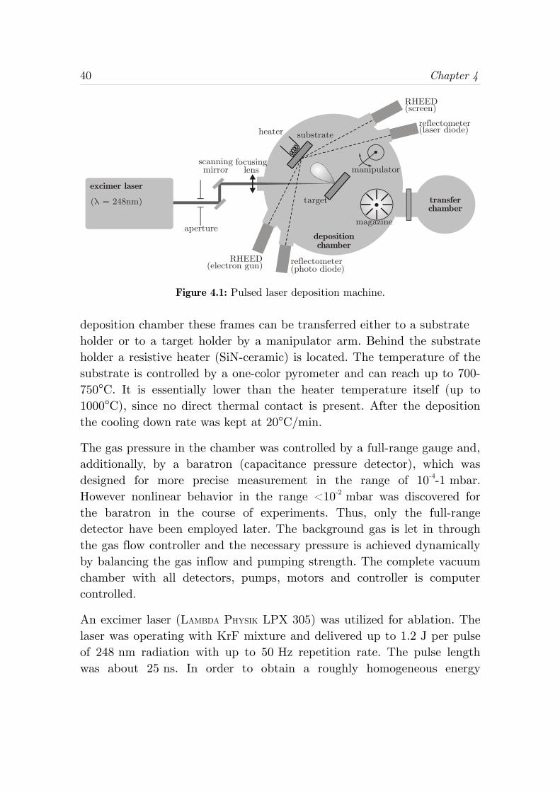
40 Chapter 4
deposition chamber these frames can be transferred either to a substrateholder or to a target holder by a manipulator arm. Behind the substrateholder a resistive heater (SiN-ceramic) is located. The temperature of thesubstrate is controlled by a one-color pyrometer and can reach up to 700-750°C. It is essentially lower than the heater temperature itself (up to1000°C), since no direct thermal contact is present. After the depositionthe cooling down rate was kept at 20°C/min.
The gas pressure in the chamber was controlled by a full-range gauge and,additionally, by a baratron (capacitance pressure detector), which wasdesigned for more precise measurement in the range of 10-4-1 mbar.However nonlinear behavior in the range <10-2 mbar was discovered forthe baratron in the course of experiments. Thus, only the full-rangedetector have been employed later. The background gas is let in throughthe gas flow controller and the necessary pressure is achieved dynamicallyby balancing the gas inflow and pumping strength. The complete vacuumchamber with all detectors, pumps, motors and controller is computercontrolled.
An excimer laser (LAMBDA PHYSIK LPX 305) was utilized for ablation. Thelaser was operating with KrF mixture and delivered up to 1.2 J per pulseof 248 nm radiation with up to 50 Hz repetition rate. The pulse lengthwas about 25 ns. In order to obtain a roughly homogeneous energy
Figure 4.1: Pulsed laser deposition machine.
RHEED
RHEED
manipulator
magazine
reflectometer
target
substrateheater
deposition
transfer
scanning
excimer laser
( = 248nm)λ
(photo diode)
chamber
reflectometer(laser diode)
mirror lens
(screen)
(electron gun)
chamber
aperture
Film Preparation by Pulsed Laser Deposition 41
distribution in the laser spot on the target, an aperture was used to cutoff the edges of the laser beam, where the intensity is varying strongly.Only the central part of the beam was utilized for ablation. The laserbeam was scanned over the target surface. This prevented formation ofcraters on the target surface and also ensured the homogeneous filmthickness over the whole substrate surface, since plasma plume is stronglydirected. The beam was focused onto the target with a lens (f=400 mm)placed in front of the window of the vacuum chamber. Both lens and thewindow were anti-reflection coated for 248 nm.
First a piezoelectric scanner have been utilized to tilt the mirror, whichwas used to scan the laser beam. However, this scanner was designed forhigh scanning frequencies and was not able of holding heavy mirrors. Onlysmall, 10 mm in diameter mirror could be mounted on this scanner. Thisresulted a very small aperture for the excimer laser beam, which hadapproximately 15×30 mm cross-section. Therefore a ×2.5 telescope wasused to reduce the beam size. Nevertheless only ~7% of laser energy couldbe transmitted into the chamber. Bad quality of the excimer laser beamand aberrations, due to the telescope lens, resulted in an asymmetrical,dash-like spot on the target. The focusing was kept constant and the laserfluence was varied by tuning the energy emitted by the excimer laser.
Later the piezoelectric beam scanner was replaced by a deflection unitwith two galvanometer scanners. They could bear larger mirrors resultingin an aperture of 20 mm in diameter. The telescope was not used in thiscase, consequently the laser spot on the target had rectangular form(determined by the aperture) and its size could be varied by changing thefocusing lens position.
The thickness of the growing film was controlled during deposition processby a reflectometer. It is discussed below in more detail. Also a RHEED1
equipment was installed on the PLD-machine, including a detecting screenand an electron gun with a double differential pumping stage foroperating at high chamber pressures. However, this facility was notutilized in the framework of this thesis.
1 RHEED – Reflection High Energy Electron Diffraction.
42 Chapter 4
Substrates and Targets Preparation
Sapphire, quartz, and YAG substrates used in the course of the work weresupplied by CRYSTEC GMBH (Berlin, Germany). All the substrates wereeither both-side or single-side polished with epitaxial quality. Sapphire (α-Al2O3) and quartz (α-SiO2) substrates were (0001)-oriented, since theyprovide good lattice matching with sesquioxides, as discussed below insection 4.3.2. YAG substrates were (100)-oriented. Yttria, lutetia, andscandia substrates are not available commercially. Thus, bulk crystals ofscandia, yttria, and lutetia have been grown by a heat-exchanger method(HEM), which is described in section 2.1.1. Subsequently, the crystalswere oriented using a Laue method, cut, and commercially polished withepitaxial quality at CRYSTEC GMBH. The substrates were cleaned withpressed air, before they were loaded into the machine.
Ceramic pellets, which served as targets for ablation, were prepared asfollows. The source materials in the form of powders were mixed togetherin the necessary proportion. Afterwards, powder was pressed with apressure up to 600 bar using a hydraulic press and sintered in air at1650°C for 24 hours. When a target was utilized for ablation for the firsttime, it was “cleaned” in the chamber with up to 5000 excimer laserpulses under the same conditions, as the subsequent deposition. A dummywas put into the substrate holder, so that the heater was notcontaminated.
Film Thickness Control (Reflectometry)
The thickness of deposited films was controlled in situ by a reflectometer,which consists of a laser diode and photo diode (see figure 4.1). Theintensity of the laser beam reflected from the sample in the chamber ismeasured with the photo diode, amplified with a DC-amplifier andrecorded with a computer during the whole deposition process. A specialsoftware was designed to record the reflectometer signal and to analyze itinstantly. Thus, real-time control of the film thickness was possible. Thesignal was fitted using a genetic algorithm1 with a model, which is
1 The idea of genetic algorithm lies in taking one or more sets of initialparameters, mixing and varying this sets randomly. Thus, a large number of such
Film Preparation by Pulsed Laser Deposition 43
discussed below. The excimer laser was controlled with the same software,therefore the deposition process could be set up to stop automatically atthe necessary thickness.
During the growth process the film thickness is changing. Subsequently,changes the phase shift between the light reflected from the front filmsurface and the light reflected from the film-substrate. This causes thevariation of intensity of the detected signal, resulting from the interferenceof the both reflected beams. Actually, one have to deal with infinitenumber of reflections and in detail this was discussed in section 3.2. If thefilm is not absorbing or scattering, the reflectometer signal is expected tohave a form of periodical function of the film thickness (dfilm) described byequation 3.12. Simplified it can be presented as
R=f cos 2πd
film
Pthickness
; Pthickness
=λ
2nfilm
cos θfilm
, (4.1)
where Pthickness(nm) is the period of the function, which can be calculated.The laser wavelength light (λ), incidence angle (θfilm) and refractive index(nfilm) of the film should be known.
Experimentally, the reflectometer signal was recorded as the function ofthe number of pulses of the excimer laser – I(Npulses). The followingequation was used to fit the measured signal
I =CA⋅R cos 2πZ
rate⋅N
pulses
P thickness
(4.2)
where R is the reflectometer signal as described by equation 3.12 (rxy
parameters are calculated), C is a constant shift, which can result from
parameter sets is generated. Afterwards “selection” takes place. A certainnumber of sets that give better results, in our case smaller deviation from themeasured reflectometer curve, are kept and than serve as a seed for the next“generation” of parameter sets. This process continues cyclically, until somequality condition, which can be given as a maximum allowed deviation value, isnot satisfied. In our case, since the dataset of the measured values was updatedconstantly, the fitting algorithm was running during the whole depositionprocess.
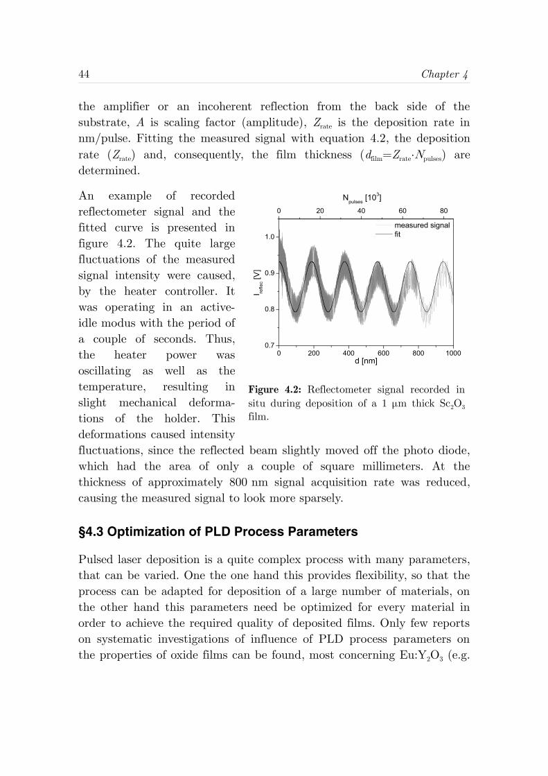
44 Chapter 4
the amplifier or an incoherent reflection from the back side of thesubstrate, A is scaling factor (amplitude), Zrate is the deposition rate innm/pulse. Fitting the measured signal with equation 4.2, the depositionrate (Zrate) and, consequently, the film thickness (dfilm=Zrate⋅Νpulses) aredetermined.
An example of recordedreflectometer signal and thefitted curve is presented infigure 4.2. The quite largefluctuations of the measuredsignal intensity were caused,by the heater controller. Itwas operating in an active-idle modus with the period ofa couple of seconds. Thus,the heater power wasoscillating as well as thetemperature, resulting inslight mechanical deforma-tions of the holder. Thisdeformations caused intensityfluctuations, since the reflected beam slightly moved off the photo diode,which had the area of only a couple of square millimeters. At thethickness of approximately 800 nm signal acquisition rate was reduced,causing the measured signal to look more sparsely.
§4.3 Optimization of PLD Process Parameters
Pulsed laser deposition is a quite complex process with many parameters,that can be varied. One the one hand this provides flexibility, so that theprocess can be adapted for deposition of a large number of materials, onthe other hand this parameters need be optimized for every material inorder to achieve the required quality of deposited films. Only few reportson systematic investigations of influence of PLD process parameters onthe properties of oxide films can be found, most concerning Eu:Y2O3 (e.g.
Figure 4.2: Reflectometer signal recorded insitu during deposition of a 1 μm thick Sc2O3
film.
0 200 400 600 800 10000.7
0.8
0.9
1.0
0 20 40 60 80
Npulses [103]
I refle
c [V]
d [nm]
measured signal fit
Film Preparation by Pulsed Laser Deposition 45
[Lan04]). The research into the PLD fabrication of Y2O3 films is alsopresented in the theses of Burmester [Bur02] and Bär [Bär04]. Thedeposition of gadolinium-gallium garnet (GGG) and Ti:sapphire films hasbeen investigated in the theses of Barrington [Bar01] and Anderson[And98].
Rare-earth scandia is an interesting active material due to its favorablespectroscopic properties, which are discussed more detailed in chapters 6and 7. Up to now, no reports on PLD fabricated Sc2O3 films can be found.Hence, a systematic analysis of the influence of PLD process parameterson the properties of Sc2O3 films was performed in order to determineoptimal conditions for the film fabrication.
4.3.1 Laser and Target
Laser
The properties of the laser radiation used for ablation influencesubstantially the character of ablation process. Usually, it is desired, thatthe absorption of laser pulse occurs in the smallest possible volume. Thisensures, that all the removed material is completely evaporated, so thatas little particulates as possible are formed. Thus, the typicalrequirements are short wavelength radiation, ideally below thefundamental absorption edge, where the linear absorption is high.Another possibility is to use intense ultrashort pulses in the femtosecondrange, where nonlinear absorption plays the major role. Theoretical andexperimental considerations of different ablation regimes, depending onwavelength and pulses duration of the laser, can be for example found inreview by A. Vogel et. al [Vog05].
In our case a KrF excimer laser was used, therefore the laser wavelengthand the pulse duration were fixed (λ=248 nm, τ=20 ns) and noexperiments could be carried out to investigate their influence on thefilms characteristics. However, this kind of laser is typically used for suchapplications and a number of reports on successful fabrication of oxidematerials with excimer lasers can be found in the literature.
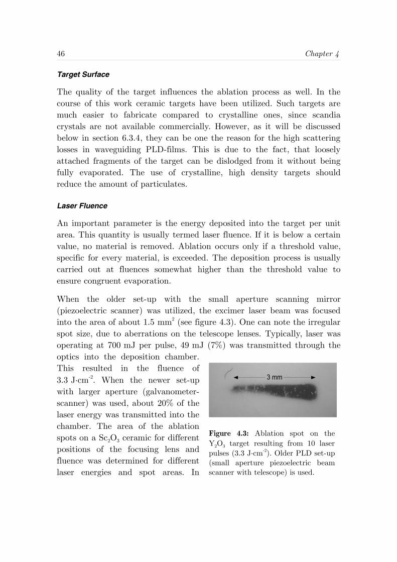
46 Chapter 4
Target Surface
The quality of the target influences the ablation process as well. In thecourse of this work ceramic targets have been utilized. Such targets aremuch easier to fabricate compared to crystalline ones, since scandiacrystals are not available commercially. However, as it will be discussedbelow in section 6.3.4, they can be one the reason for the high scatteringlosses in waveguiding PLD-films. This is due to the fact, that looselyattached fragments of the target can be dislodged from it without beingfully evaporated. The use of crystalline, high density targets shouldreduce the amount of particulates.
Laser Fluence
An important parameter is the energy deposited into the target per unitarea. This quantity is usually termed laser fluence. If it is below a certainvalue, no material is removed. Ablation occurs only if a threshold value,specific for every material, is exceeded. The deposition process is usuallycarried out at fluences somewhat higher than the threshold value toensure congruent evaporation.
When the older set-up with the small aperture scanning mirror(piezoelectric scanner) was utilized, the excimer laser beam was focusedinto the area of about 1.5 mm2 (see figure 4.3). One can note the irregularspot size, due to aberrations on the telescope lenses. Typically, laser wasoperating at 700 mJ per pulse, 49 mJ (7%) was transmitted through theoptics into the deposition chamber.This resulted in the fluence of3.3 J⋅cm-2. When the newer set-upwith larger aperture (galvanometer-scanner) was used, about 20% of thelaser energy was transmitted into thechamber. The area of the ablationspots on a Sc2O3 ceramic for differentpositions of the focusing lens andfluence was determined for differentlaser energies and spot areas. In
Figure 4.3: Ablation spot on theY2O3 target resulting from 10 laserpulses (3.3 J⋅cm-2). Older PLD set-up(small aperture piezoelectric beamscanner with telescope) is used.
3 mm
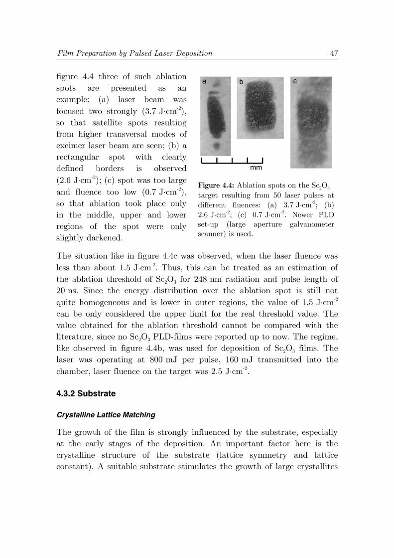
Film Preparation by Pulsed Laser Deposition 47
figure 4.4 three of such ablationspots are presented as anexample: (a) laser beam wasfocused two strongly (3.7 J⋅cm-2),so that satellite spots resultingfrom higher transversal modes ofexcimer laser beam are seen; (b) arectangular spot with clearlydefined borders is observed(2.6 J⋅cm-2); (c) spot was too largeand fluence too low (0.7 J⋅cm-2),so that ablation took place onlyin the middle, upper and lowerregions of the spot were onlyslightly darkened.
The situation like in figure 4.4c was observed, when the laser fluence wasless than about 1.5 J⋅cm-2. Thus, this can be treated as an estimation ofthe ablation threshold of Sc2O3 for 248 nm radiation and pulse length of20 ns. Since the energy distribution over the ablation spot is still notquite homogeneous and is lower in outer regions, the value of 1.5 J⋅cm-2
can be only considered the upper limit for the real threshold value. Thevalue obtained for the ablation threshold cannot be compared with theliterature, since no Sc2O3 PLD-films were reported up to now. The regime,like observed in figure 4.4b, was used for deposition of Sc2O3 films. Thelaser was operating at 800 mJ per pulse, 160 mJ transmitted into thechamber, laser fluence on the target was 2.5 J⋅cm-2.
4.3.2 Substrate
Crystalline Lattice Matching
The growth of the film is strongly influenced by the substrate, especiallyat the early stages of the deposition. An important factor here is thecrystalline structure of the substrate (lattice symmetry and latticeconstant). A suitable substrate stimulates the growth of large crystallites
Figure 4.4: Ablation spots on the Sc2O3
target resulting from 50 laser pulses atdifferent fluences: (a) 3.7 J⋅cm-2; (b)2.6 J⋅cm-2; (c) 0.7 J⋅cm-2. Newer PLDset-up (large aperture galvanometerscanner) is used.
a b c
mm
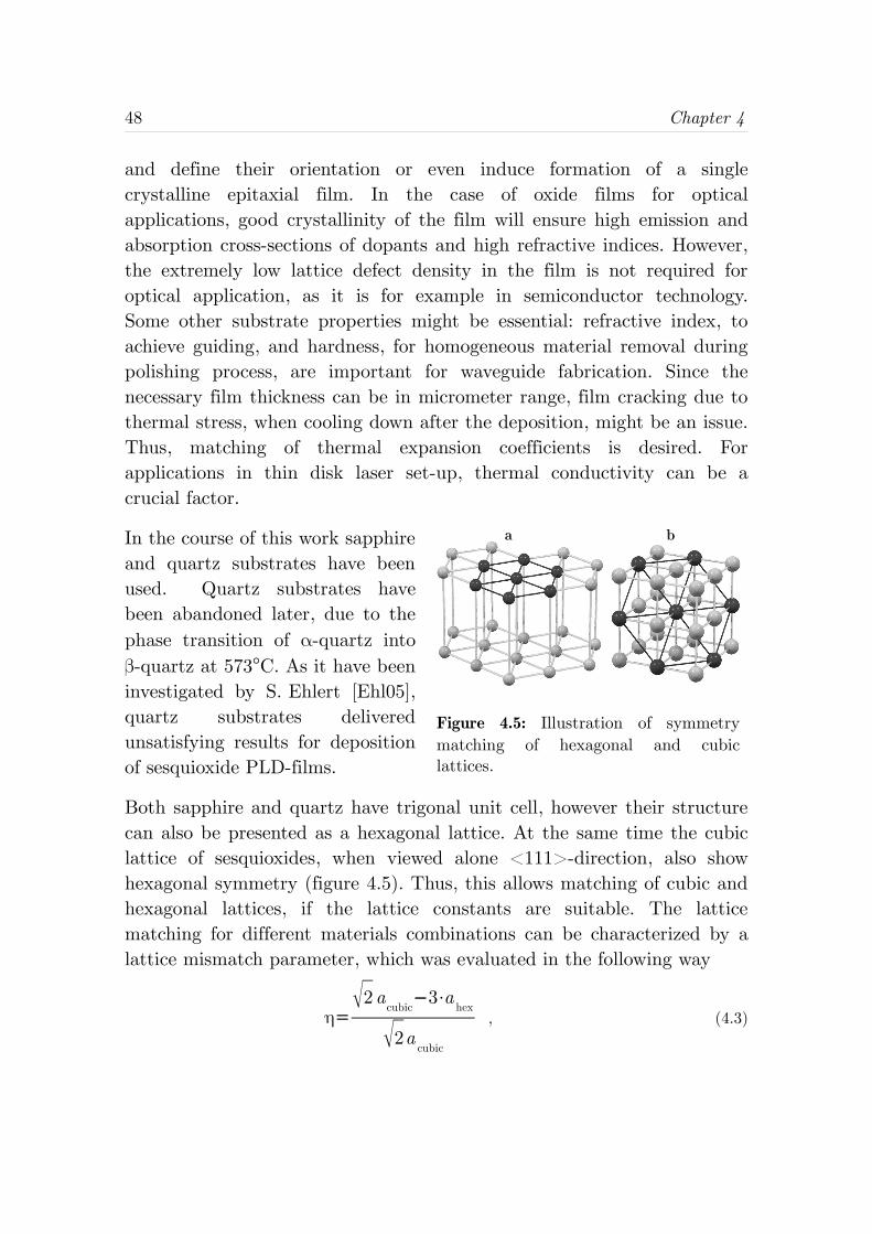
48 Chapter 4
and define their orientation or even induce formation of a singlecrystalline epitaxial film. In the case of oxide films for opticalapplications, good crystallinity of the film will ensure high emission andabsorption cross-sections of dopants and high refractive indices. However,the extremely low lattice defect density in the film is not required foroptical application, as it is for example in semiconductor technology.Some other substrate properties might be essential: refractive index, toachieve guiding, and hardness, for homogeneous material removal duringpolishing process, are important for waveguide fabrication. Since thenecessary film thickness can be in micrometer range, film cracking due tothermal stress, when cooling down after the deposition, might be an issue.Thus, matching of thermal expansion coefficients is desired. Forapplications in thin disk laser set-up, thermal conductivity can be acrucial factor.
In the course of this work sapphireand quartz substrates have beenused. Quartz substrates havebeen abandoned later, due to thephase transition of α-quartz intoβ-quartz at 573°C. As it have beeninvestigated by S. Ehlert [Ehl05],quartz substrates deliveredunsatisfying results for depositionof sesquioxide PLD-films.
Both sapphire and quartz have trigonal unit cell, however their structurecan also be presented as a hexagonal lattice. At the same time the cubiclattice of sesquioxides, when viewed alone <111>-direction, also showhexagonal symmetry (figure 4.5). Thus, this allows matching of cubic andhexagonal lattices, if the lattice constants are suitable. The latticematching for different materials combinations can be characterized by alattice mismatch parameter, which was evaluated in the following way
η=2a
cubic3⋅a
hex
2acubic
, (4.3)
Figure 4.5: Illustration of symmetrymatching of hexagonal and cubiclattices.
a b
Film Preparation by Pulsed Laser Deposition 49
where acubic is the lattice constantof cubic sesquioxides and ahex issapphire or quartz latticeconstant, which denotes thehexagon side. The mismatch incase of Sc2O3 and α-Al2O3
substrate is about 2.6%. It isalso in the range of severalpercents for other materialcombinations (see table 4.1). It can be reduced by mixing two cationswith different radii, e.g. mixing Sc3+ and Lu3+ in 1:1 proportion will giveonly 0.17% misfit.
The refractive indices of sesquioxides in the visible region are in the rangeof 1.9-2.0. Refractive index of both sapphire and quartz are lower. Thisfact opens the possibility of light guiding in sesquioxide films deposited onquartz or sapphire substrates. In detail the waveguiding properties ofsesquioxide films are discussed in chapter 6. Essential characteristics ofsubstrate and film materials used in this work can be found in table 2.2.
Substrate Temperature
The temperature of the substrate determines the mobility of ions on thefilm surface. It has dramatical effect on crystallinity of the film.
A series of 500 nm thick Sc2O3 films1 have been deposited at differentsubstrate temperatures in order to investigate the influence of thisparameter on the film properties. Except for the temperature, which haschanged through the values 20°C, 300°C, 500°C, and 700°C, all the otherdeposition parameters have been maintained constant: PO2=1×10⁻³ mbar,Φ=2.5 J⋅cm-2, dsub-targ=9.5 cm.
The results of high resolution θ-2θ scans and rocking-curve measurementsof the <222> reflection peak as well as the results of scattering and
1 The samples L06-L08, L10 are discussed. Here and further in the footnotes, thesamples are mentioned as they are denoted in the list of fabricated samples inappendix A.
Table 4.1. Lattice mismatch parameter(in %) for sesquioxide films onsapphire and quartzsubstrates.
Y2O3 Sc2O3 Lu2O3 ScLuO3
α-Al2O3 4.74 -2.62 2.82 0.17
α-SiO2 1.74 -5.85 -0.25 -2.97
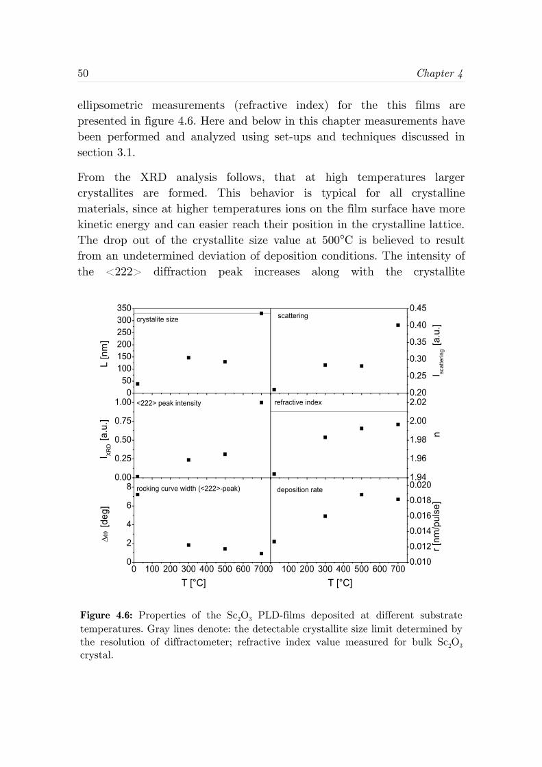
50 Chapter 4
ellipsometric measurements (refractive index) for the this films arepresented in figure 4.6. Here and below in this chapter measurements havebeen performed and analyzed using set-ups and techniques discussed insection 3.1.
From the XRD analysis follows, that at high temperatures largercrystallites are formed. This behavior is typical for all crystallinematerials, since at higher temperatures ions on the film surface have morekinetic energy and can easier reach their position in the crystalline lattice.The drop out of the crystallite size value at 500°C is believed to resultfrom an undetermined deviation of deposition conditions. The intensity ofthe <222> diffraction peak increases along with the crystallite
Figure 4.6: Properties of the Sc2O3 PLD-films deposited at different substratetemperatures. Gray lines denote: the detectable crystallite size limit determined bythe resolution of diffractometer; refractive index value measured for bulk Sc2O3
crystal.
050
100150200250300350
L [n
m]
0.20
0.25
0.30
0.35
0.40
0.45
refractive index
deposition raterocking curve width (<222>-peak)
crystalite size
<222> peak intensity
I scat
terin
g [a
.u.]
scattering
0.00
0.25
0.50
0.75
1.00
I XR
D [a
.u.]
1.94
1.96
1.98
2.00
2.02
n
0 100 200 300 400 500 600 7000
2
4
6
8
Δω [d
eg]
T [°C]0 100 200 300 400 500 600 700
0.010
0.012
0.014
0.016
0.018
0.020
r [n
m/p
ulse
]
T [°C]
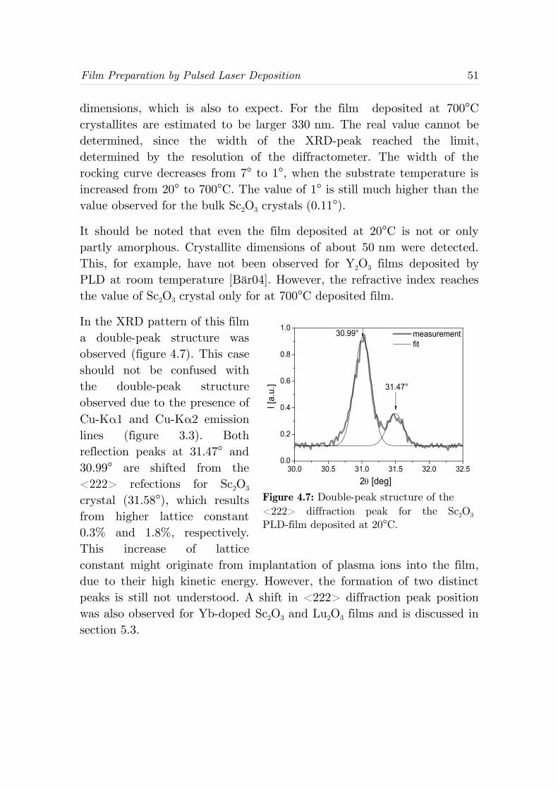
Film Preparation by Pulsed Laser Deposition 51
dimensions, which is also to expect. For the film deposited at 700°Ccrystallites are estimated to be larger 330 nm. The real value cannot bedetermined, since the width of the XRD-peak reached the limit,determined by the resolution of the diffractometer. The width of therocking curve decreases from 7° to 1°, when the substrate temperature isincreased from 20° to 700°C. The value of 1° is still much higher than thevalue observed for the bulk Sc2O3 crystals (0.11°).
It should be noted that even the film deposited at 20°C is not or onlypartly amorphous. Crystallite dimensions of about 50 nm were detected.This, for example, have not been observed for Y2O3 films deposited byPLD at room temperature [Bär04]. However, the refractive index reachesthe value of Sc2O3 crystal only for at 700°C deposited film.
In the XRD pattern of this filma double-peak structure wasobserved (figure 4.7). This caseshould not be confused withthe double-peak structureobserved due to the presence ofCu-Kα1 and Cu-Kα2 emissionlines (figure 3.3). Bothreflection peaks at 31.47° and30.99° are shifted from the<222> refections for Sc2O3
crystal (31.58°), which resultsfrom higher lattice constant0.3% and 1.8%, respectively.This increase of latticeconstant might originate from implantation of plasma ions into the film,due to their high kinetic energy. However, the formation of two distinctpeaks is still not understood. A shift in <222> diffraction peak positionwas also observed for Yb-doped Sc2O3 and Lu2O3 films and is discussed insection 5.3.
Figure 4.7: Double-peak structure of the<222> diffraction peak for the Sc2O3
PLD-film deposited at 20°C.
30.0 30.5 31.0 31.5 32.0 32.50.0
0.2
0.4
0.6
0.8
1.030.99°
I [a.
u.]
2θ [deg]
measurement fit
31.47°
52 Chapter 4
4.3.3 Background Atmosphere
A reactive ambient atmosphere during the deposition is often used toimprove the composition of the PLD-films. Since oxide films aredeposited, the natural choice for the background gas is oxygen, whichensures that films are not O2-deficient. Background gas is also used tocontrol the energy of plasma particles, which can affect the film growthregime.
The partial oxygen pressure in the deposition chamber have been changedthough the series1 of Sc2O3 films to investigate its impact on the filmproperties. The other deposition parameters were maintained constant:Tsub=700°C, dtarg-sub=9.5 cm, Φ=2.5 J⋅cm-2. All the films were deposited onsapphire substrates and were 500 nm thick. According to the resultspresented in figure 4.9, one can separate three regimes for deposition ofSc2O3. In the range of oxygen pressures from 10-3 mbar to 10-2 mbarcrystalline films with almost identical properties were produced. Thecrystallite dimensions reached 330 nm. No estimation could be madebeyond this limit (shown as a gray line), which is determined by thediffractometer resolution (see section 3.1). The rocking curve, showed thewidth of about 1°. The refractive index reached the value of the bulkcrystal presented as a gray line in the figure It is ~0.02 higher as therefractive index obtained from the Sellmeier equation (1.989 at 632.8 nm).
At the lower oxygen pressure (<10-3 mbar), which means higher kineticenergies of plasma particles, crystallites only up to 100 nm are build. Therocking curve is also broader (~2°). These both effects can be understoodthrough the bombardment of the film by high energetic plasma particles,which produce higher density of crystallization centers. They also partlydestroy the lattice of the already deposited film and break the orientationgiven by the underlying layers. Dense films are produced, which isconfirmed by their high refractive index.
For oxygen pressure over 10-2 mbar the properties of the deposited filmschange essentially. The XRD analysis reveals, that beside the <222>diffraction peak also the <400> diffraction peak appear. For the films
1 L09-L16 (appendix A).
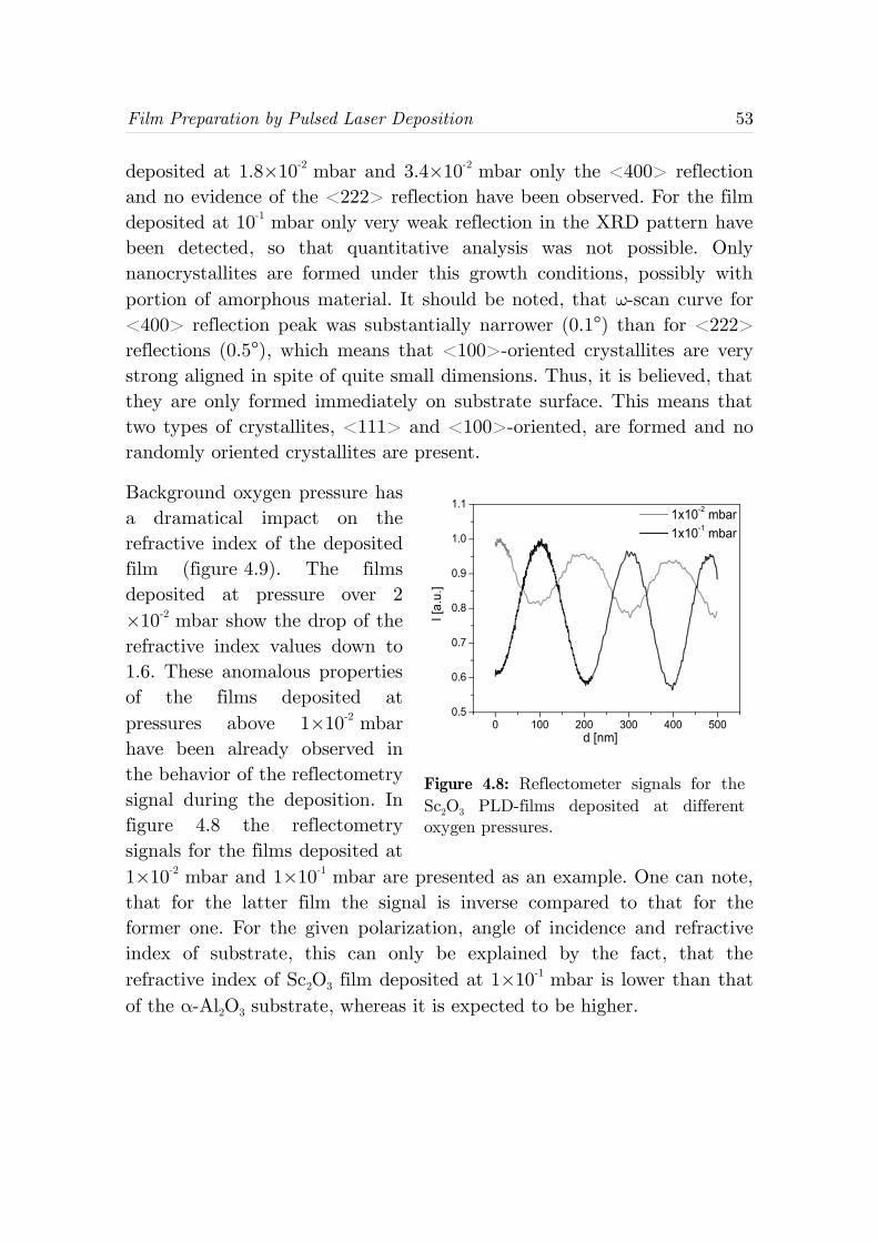
Film Preparation by Pulsed Laser Deposition 53
deposited at 1.8×10⁻² mbar and 3.4×10⁻² mbar only the <400> reflectionand no evidence of the <222> reflection have been observed. For the filmdeposited at 10-1 mbar only very weak reflection in the XRD pattern havebeen detected, so that quantitative analysis was not possible. Onlynanocrystallites are formed under this growth conditions, possibly withportion of amorphous material. It should be noted, that ω-scan curve for<400> reflection peak was substantially narrower (0.1°) than for <222>reflections (0.5°), which means that <100>-oriented crystallites are verystrong aligned in spite of quite small dimensions. Thus, it is believed, thatthey are only formed immediately on substrate surface. This means thattwo types of crystallites, <111> and <100>-oriented, are formed and norandomly oriented crystallites are present.
Background oxygen pressure hasa dramatical impact on therefractive index of the depositedfilm (figure 4.9). The filmsdeposited at pressure over 2×10⁻² mbar show the drop of therefractive index values down to1.6. These anomalous propertiesof the films deposited atpressures above 1×10⁻² mbarhave been already observed inthe behavior of the reflectometrysignal during the deposition. Infigure 4.8 the reflectometrysignals for the films deposited at1×10-2 mbar and 1×10⁻¹ mbar are presented as an example. One can note,that for the latter film the signal is inverse compared to that for theformer one. For the given polarization, angle of incidence and refractiveindex of substrate, this can only be explained by the fact, that therefractive index of Sc2O3 film deposited at 1×10⁻¹ mbar is lower than thatof the α-Al2O3 substrate, whereas it is expected to be higher.
Figure 4.8: Reflectometer signals for theSc2O3 PLD-films deposited at differentoxygen pressures.
0 100 200 300 400 5000.5
0.6
0.7
0.8
0.9
1.0
1.1
I [a.
u.]
d [nm]
1x10⁻² mbar 1x10⁻¹ mbar
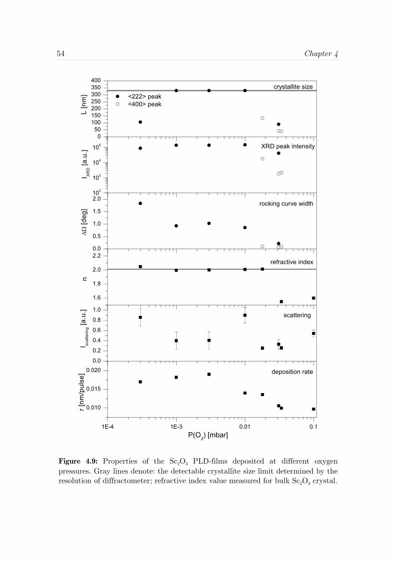
54 Chapter 4
Figure 4.9: Properties of the Sc2O3 PLD-films deposited at different oxygenpressures. Gray lines denote: the detectable crystallite size limit determined by theresolution of diffractometer; refractive index value measured for bulk Sc2O3 crystal.
1E-4 1E-3 0.01 0.1
0.010
0.015
0.020
r [nm
/pul
se]
P(O2) [mbar]
0.0
0.2
0.4
0.6
0.8
1.0
I scat
terin
g [a.u
.]
1.6
1.8
2.0
2.2
n
0.0
0.5
1.0
1.5
2.0
ΔΩ
[deg
]
102
103
104
105
I XR
D [a
.u.]
050
100150200250300350400
deposition rate
scattering
refractive index
rocking curve width
XRD peak intensity
L [n
m] <222> peak
<400> peak
crystallite size
Film Preparation by Pulsed Laser Deposition 55
4.3.4 Summary and Discussion
In this section Sc2O3 PLD-films and influence of PLD process parameteron their properties have been discussed.
Ablation threshold of Sc2O3 ceramic target for KrF excimer laser radiation(248 nm, 20 ns) has been estimated to be <1.5 J⋅cm-2. Thus, somewhathigher fluence of 2.5 J⋅cm-2 have been used for deposition of the films.
Deposition at different substrate temperatures has revealed, that even at20°C (room temperature) films were not completely amorphous andcrystallites with dimensions of about 50 nm have been detected.Crystallites with slightly larger lattice constant (up to 1.8%) have beenobserved in the RT-deposited film in addition to crystallites with typicalSc2O3 lattice. This was explained by implantation into the lattice of highenergetic plasma particles. At 700°C films were highly <111>-texturedand crystallites in the range of several hundreds of nanometers (>330 nm)have been observed. Real dimensions could not be determined due to thelimited resolution of the used diffractometer.
Depending on the background oxygen pressure three film growth modeswere observed: for pressures in the range 10-3 mbar – 10-2 mbar largecrystallites (>330 nm) grew, for pressures lower 10-3 mbar, dense filmswith smaller crystallite dimensions (~100 nm) were formed, and forpressures higher than 10-2 mbar not quite dense films with low refractiveindex (~1.6) were observed. In the latter case <100>-oriented crystalliteswere detected in addition to typically observed <111>-orientedcrystallites.
The dramatic change of film properties, when background oxygen pressureis raised over 10-2 mbar during the deposition, can be explained byformation of a nonsteady shock front (also called a blast wave). It isformed, when pressure of the expanding plume reaches the pressure of thebackground gas [Sae93b]. Inside of the plume the particles have highkinetic energies (ultrasonic expansion), which is typical for pulsed laserdeposition. Behind this front the particles are thermalized and depositionwill have thermal character, like by normal thermal evaporationtechniques. With the increasing background gas pressure the plume is
56 Chapter 4
getting more confined, the effect become more pronounced and theposition, where the shock front is formed, moves closer to the target. Inour case, at the pressure of approximately 3×10⁻² mbar and given laserfluence, the shock front formed as close to the target as 9.5 cm. Thus, atthe higher pressures the deposition regime is more like by thermalevaporation. Plasma particles are thermalized and do not posses highkinetic energy. This causes amorphous, not very dense films with lowrefractive index to be produced. Low kinetic energy particles also cannotdeposit enough energy to stimulate the growth of large crystallites. Theformation of a shock front has been also observed, for example, during thelaser ablation of high temperature superconductors [Sco90, Gup91]. Theeffect of refractive index change can be for example utilized to producephotonic structures (like Bragg mirrors) or waveguides using a singlematerial, deposited under different conditions.
Another effect observed due to the increase of the background oxygenpressure is a drop of the deposition rate (figure 4.9). However, it shouldbe mentioned, that in some case change of the deposition rate, cannot beexplained by obvious change in deposition conditions, like for the series offilms deposited at different substrate temperatures (figure 4.6). Thus, itwas found that the deposition conditions were not fully reproducible. Twopossible reasons for this behavior were later identified. Aging of theexcimer gas laser caused higher voltage to be applied to achieve thepredefined energy per pulse. Due to the thermal effects the laser beamprofile varied. Consequently, changes in the ablation spot shape on thetarget were observed. Also modification of target surface in the course ofthe ablation influenced the deposition process.
The intensity of scattered light measured using integrating sphere do notreveal distinct dependency on any deposition parameter or filmcharacteristics, except for substrate temperature (figure 4.6). The valuesare statistically distributed, as for example presented in figure 4.9 foroxygen pressure. Thus, it was concluded that this technique is not quitesuitable for estimation of scattering in the PLD-films.
Summarizing the results of this section, the highest crystalline quality ofthe films was obtained for the substrate temperature of 700°C,

Film Preparation by Pulsed Laser Deposition 57
background oxygen pressure of 10-3 mbar - 10-2 mbar, for the laser fluenceof 2.5 J⋅cm-2 and the target-substrate distance of 9.5 cm. The temperatureof 700°C degrees is the maximal achievable temperature. As it is discussedin sections 7.2.2 and 7.2.3, the higher deposition temperatures canpossibly improve the film quality.
Chapter 5. X-ray Diffraction Analysis
In this chapter the results of structural characterization of ytterbia, YAG,scandia, and lutetia PLD-films by means of X-ray diffraction arepresented. The crystalline quality of the deposited films is an importantfactor for active materials doped with rare-earth ions. The peak emissionand absorption cross-sections and the excited states lifetimes of thedopants strongly depend on the quality of the crystalline lattice of thehost material. Since high gain materials are preferred in order to reducethe size of active elements, high quality crystalline films are required.Moreover, an oriented crystalline growth can be desired in some cases, e.g.in order to reduce light scattering at the grain boundaries.
The XRD measurements in this chapter and their analysis were performedas described in section 3.1.
§5.1 Ytterbia Films
The ytterbia films1 with thicknesses in the range of 20-500 nm have beendeposited on sapphire and quartz substrates. The oxygen pressure duringthe deposition was 1×10⁻² mbar, the substrate temperature was 700°C,and the target-substrate distance about 8 cm. The laser fluence on thetarget was 3.3 J⋅cm-2. The spectroscopic properties of the ytterbia filmsare discussed later in section 7.2.1.
The X-ray diffraction patterns of the films are presented in figures 5.1 and5.2, respectively, for the films deposited on (0001)-cut sapphire and quartzsubstrates. All the films reveal only <222> and <444> reflection peakswith no visible hints on other orientations. It should be noted, that thediffraction peaks are generally stronger for the films deposited on α-Al2O3
1 Y01, Y02, Y04 and Y07-Y09 (appendix A).
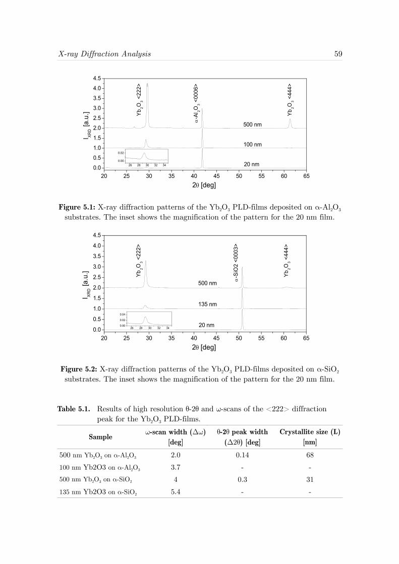
X-ray Diffraction Analysis 59
Figure 5.1: X-ray diffraction patterns of the Yb2O3 PLD-films deposited on α-Al2O3
substrates. The inset shows the magnification of the pattern for the 20 nm film.
Figure 5.2: X-ray diffraction patterns of the Yb2O3 PLD-films deposited on α-SiO2
substrates. The inset shows the magnification of the pattern for the 20 nm film.
Table 5.1. Results of high resolution θ-2θ and ω-scans of the <222> diffractionpeak for the Yb2O3 PLD-films.
Sampleω-scan width (Δω)
[deg]θ-2θ peak width
(Δ2θ) [deg]Crystallite size (L)
[nm]
500 nm Yb2O3 on α-Al2O3 2.0 0.14 68
100 nm Yb2O3 on α-Al2O3 3.7 - -
500 nm Yb2O3 on α-SiO2 4 0.3 31
135 nm Yb2O3 on α-SiO2 5.4 - -
20 25 30 35 40 45 50 55 60 650.0
0.5
1.0
1.5
2.0
2.5
3.0
3.5
4.0
4.5
26 28 30 32 340.00
0.02
20 nm
100 nm
Yb2O
3 <44
4>
Yb2O
3 <22
2>
I XRD [a
.u.]
2θ [deg]α
-Al 2O
3 <00
06>
500 nm
20 25 30 35 40 45 50 55 60 650.0
0.5
1.0
1.5
2.0
2.5
3.0
3.5
4.0
4.5
26 28 30 32 340.00
0.02
0.04
20 nm
135 nm
Yb2O
3 <44
4>
Yb2O
3 <22
2>
I XRD [a
.u.]
2θ [deg]
α-S
iO2
<000
3>
500 nm
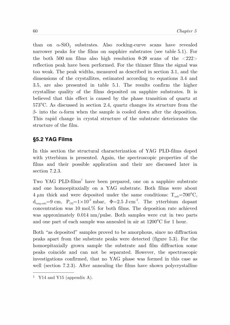
60 Chapter 5
than on α-SiO2 substrates. Also rocking-curve scans have revealednarrower peaks for the films on sapphire substrates (see table 5.1). Forthe both 500 nm films also high resolution θ-2θ scans of the <222>reflection peak have been performed. For the thinner films the signal wastoo weak. The peak widths, measured as described in section 3.1, and thedimensions of the crystallites, estimated according to equations 3.4 and3.5, are also presented in table 5.1. The results confirm the highercrystalline quality of the films deposited on sapphire substrates. It isbelieved that this effect is caused by the phase transition of quartz at573°C. As discussed in section 2.4, quartz changes its structure from theβ- into the α-form when the sample is cooled down after the deposition.This rapid change in crystal structure of the substrate deteriorates thestructure of the film.
§5.2 YAG Films
In this section the structural characterization of YAG PLD-films dopedwith ytterbium is presented. Again, the spectroscopic properties of thefilms and their possible application and their are discussed later insection 7.2.3.
Two YAG PLD-films1 have been prepared, one on a sapphire substrateand one homoepitaxially on a YAG substrate. Both films were about4 μm thick and were deposited under the same conditions: Tsub=700°C,dtarg-sub=9 cm, PO2=1×10⁻² mbar, Φ=2.5 J⋅cm-2. The ytterbium dopantconcentration was 10 mol.% for both films. The deposition rate achievedwas approximately 0.014 nm/pulse. Both samples were cut in two partsand one part of each sample was annealed in air at 1200°C for 1 hour.
Both “as deposited” samples proved to be amorphous, since no diffractionpeaks apart from the substrate peaks were detected (figure 5.3). For thehomoepitaxially grown sample the substrate and film diffraction somepeaks coincide and can not be separated. However, the spectroscopicinvestigations confirmed, that no YAG phase was formed in this case aswell (section 7.2.3). After annealing the films have shown polycrystalline
1 Y14 and Y15 (appendix A).
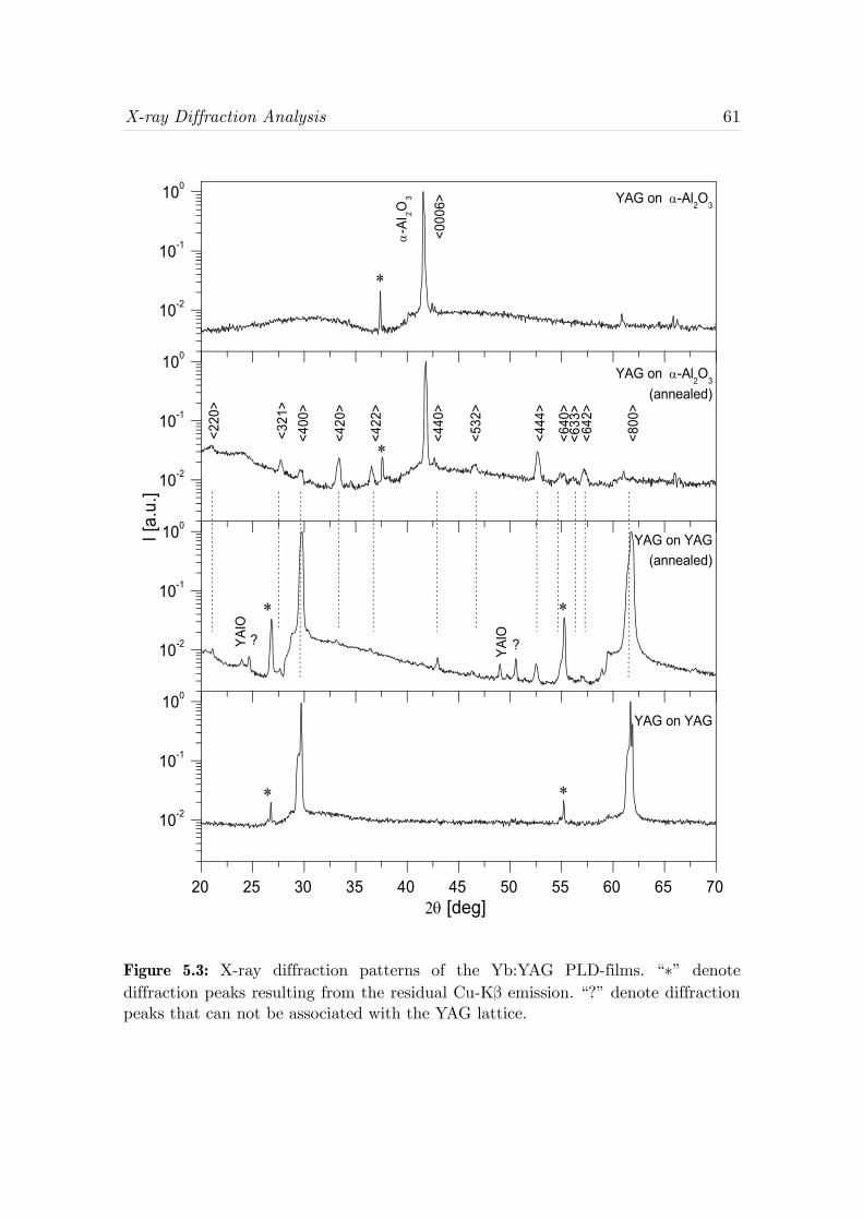
X-ray Diffraction Analysis 61
Figure 5.3: X-ray diffraction patterns of the Yb:YAG PLD-films. “∗” denotediffraction peaks resulting from the residual Cu-Kβ emission. “?” denote diffractionpeaks that can not be associated with the YAG lattice.
20 25 30 35 40 45 50 55 60 65 70
10-2
10-1
100
2θ [deg]
10-2
10-1
100
I [a.
u.] 10-2
10-1
100
∗
∗
∗
∗∗
∗
10-2
10-1
100
YAlO
(annealed)
YAG on YAG
??
<321
>
YAlO
YAG on YAG
(annealed)
YAG on α-Al2O3
α-A
l 2O3
<00
06>
<633
>
<800
>
<640
><6
42>
<532
>
<422
>
<220
>
<444
>
<420
>
<400
>
YAG on α-Al2O3
<440
>
62 Chapter 5
behavior. A number of diffraction peaks, characteristic for the YAGstructure, have been detected. All the peaks are very weak and quitebroad, which indicates that only crystallites with dimensions in thenanometer range have been formed. The YAG film grown homoepitaxiallyalso revealed some peaks that could not be associated with the YAGlattice. Some of them can be assigned to the YAlO3 - perovskite phase ofthe Y-Al-O mixture. The annealed films show spectroscopic propertiessimilar to that of the Yb:YAG bulk crystal. Thus, it can be concludedthat the temperature of 700°C is not sufficient for the YAG crystalstructure to be formed and that temperatures up to 1200°C are needed tothermally initiate the growth of YAG crystallites.
§5.3 Lutetia and Scandia Films
This section presents the results of structural investigations of ytterbium-doped lutetia and scandia films1 by X-ray diffraction. The spectroscopicproperties of the films are discussed later in section 7.2.2. Two Yb:Lu2O3
films have been deposited on a (0001)-oriented α-Al2O3 and on a(111)-oriented Lu2O3 substrates, respectively. In the similar way twoYb:Sc2O3 films have been produced on a (0001)-oriented α-Al2O3 and on a(111)-oriented Sc2O3 substrates. The Yb3+ concentration was 5 mol.% and4 mol.% for Lu2O3 and for Sc2O3 films, respectively. The films have beenproduced under the same conditions as the YAG films discussed above insection 7.2.3. The lutetia films were 3.3 μm and 3.5 μm thick for the filmsdeposited on sapphire and on lutetia substrates, respectively. Bothscandia films were 4 μm thick. The films deposited on sapphire substrateswere cut in two parts and one half of each sample was annealed in air at900°C for 1 hour.
Lutetia Films
In figure 5.4 the X-ray diffraction patterns for Lu2O3 films are presented.For the homoepitaxially grown film only <222> and <444> reflectionpeaks are present in the diffraction pattern. The peaks are asymmetricand broader than those of the uncoated Lu2O3 substrate. The film
1 Y10-Y13 (appendix A).
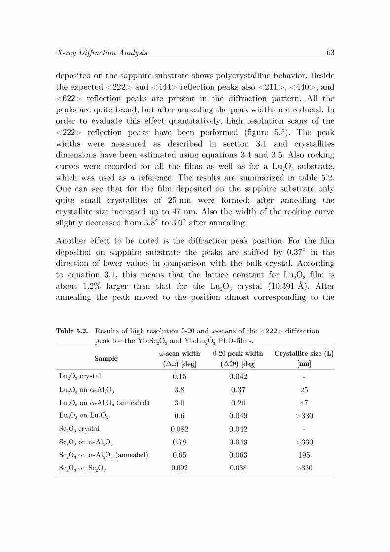
X-ray Diffraction Analysis 63
deposited on the sapphire substrate shows polycrystalline behavior. Besidethe expected <222> and <444> reflection peaks also <211>, <440>, and<622> reflection peaks are present in the diffraction pattern. All thepeaks are quite broad, but after annealing the peak widths are reduced. Inorder to evaluate this effect quantitatively, high resolution scans of the<222> reflection peaks have been performed (figure 5.5). The peakwidths were measured as described in section 3.1 and crystallitesdimensions have been estimated using equations 3.4 and 3.5. Also rockingcurves were recorded for all the films as well as for a Lu2O3 substrate,which was used as a reference. The results are summarized in table 5.2.One can see that for the film deposited on the sapphire substrate onlyquite small crystallites of 25 nm were formed; after annealing thecrystallite size increased up to 47 nm. Also the width of the rocking curveslightly decreased from 3.8° to 3.0° after annealing.
Another effect to be noted is the diffraction peak position. For the filmdeposited on sapphire substrate the peaks are shifted by 0.37° in thedirection of lower values in comparison with the bulk crystal. Accordingto equation 3.1, this means that the lattice constant for Lu2O3 film isabout 1.2% larger than that for the Lu2O3 crystal (10.391 Å). Afterannealing the peak moved to the position almost corresponding to the
Table 5.2. Results of high resolution θ-2θ and ω-scans of the <222> diffractionpeak for the Yb:Sc2O3 and Yb:Lu2O3 PLD-films.
Sampleω-scan width(Δω) [deg]
θ-2θ peak width(Δ2θ) [deg]
Crystallite size (L)[nm]
Lu2O3 crystal 0.15 0.042 -
Lu2O3 on α-Al2O3 3.8 0.37 25
Lu2O3 on α-Al2O3 (annealed) 3.0 0.20 47Lu2O3 on Lu2O3 0.6 0.049 >330Sc2O3 crystal 0.082 0.042 -
Sc2O3 on α-Al2O3 0.78 0.049 >330
Sc2O3 on α-Al2O3 (annealed) 0.65 0.063 195Sc2O3 on Sc2O3 0.092 0.038 >330
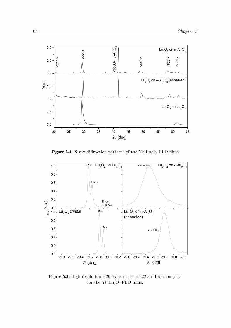
64 Chapter 5
Figure 5.4: X-ray diffraction patterns of the Yb:Lu2O3 PLD-films.
Figure 5.5: High resolution θ-2θ scans of the <222> diffraction peakfor the Yb:Lu2O3 PLD-films.
20 25 30 35 40 45 50 55 60 65
0.0
0.5
1.0
1.5
2.0
2.5
3.0
<000
6> α
-Al 2O
3
Lu2O3 on Lu2O3
Lu2O3 on α-Al2O3 (annealed)<2
22>
<211
>
<444
>
<622
>
I [a.
u.]
2θ [deg]<4
40>
Lu2O3 on α-Al2O3
0.0
0.2
0.4
0.6
0.8
1.0
(annealed)
Kα1 + Kα2
Lu2O3 on α-Al2O3
Lu2O3 on α-Al2O3
Lu2O3 crystal
I XR
D [a
.u.]
Lu2O3 on Lu2O3
Kα2
Kα1
Kα1 + Kα2
29.0 29.2 29.4 29.6 29.8 30.0 30.20.0
0.2
0.4
0.6
0.8
1.0
II Kα1
2θ [deg]2θ [deg]
I Kα2
II Kα2
I Kα1
29.0 29.2 29.4 29.6 29.8 30.0 30.2
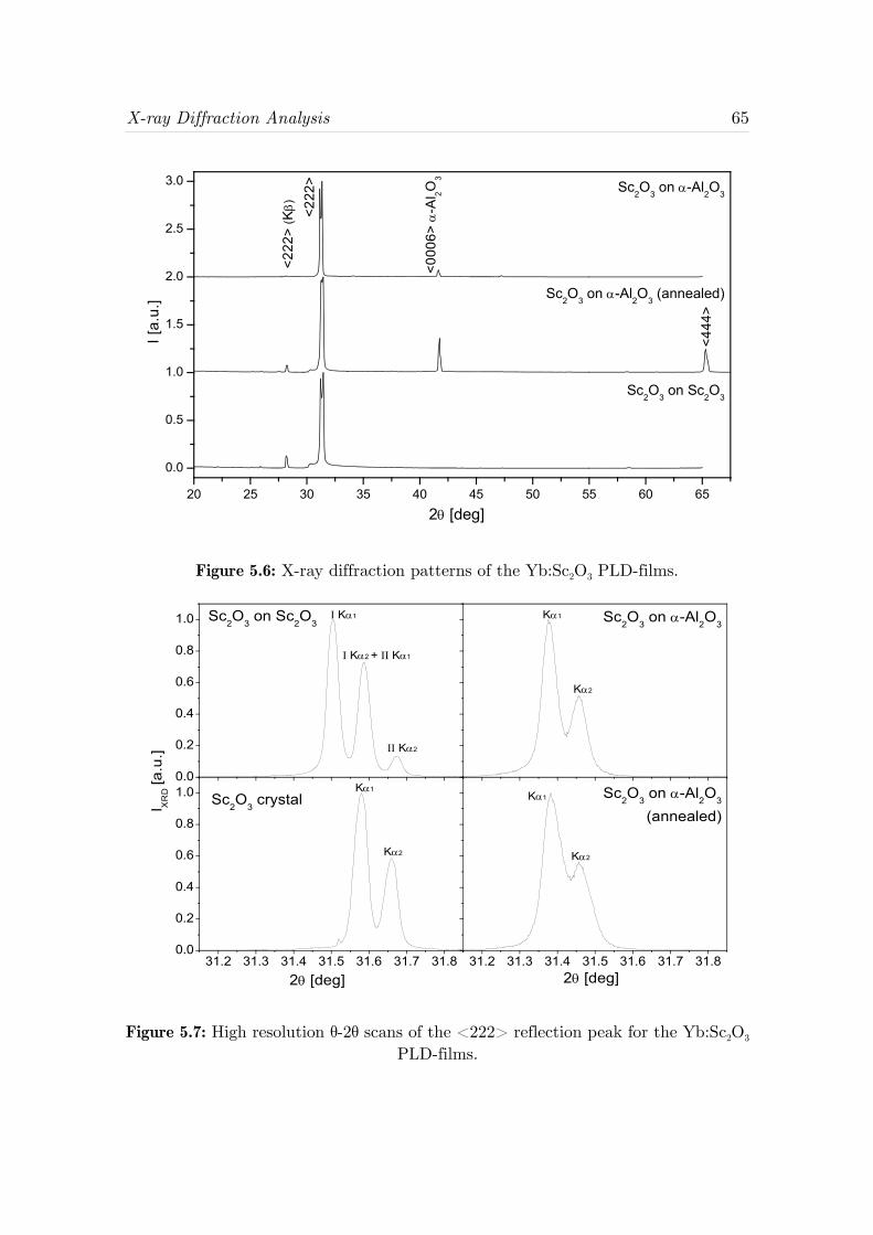
X-ray Diffraction Analysis 65
Figure 5.6: X-ray diffraction patterns of the Yb:Sc2O3 PLD-films.
Figure 5.7: High resolution θ-2θ scans of the <222> reflection peak for the Yb:Sc2O3
PLD-films.
20 25 30 35 40 45 50 55 60 65
0.0
0.5
1.0
1.5
2.0
2.5
3.0
<222
><2
22>
(Kβ)
<000
6> α
-Al 2O
3
Sc2O3 on Sc2O3
Sc2O3 on α-Al2O3 (annealed)
<444
>
I [a.
u.]
2θ [deg]
Sc2O3 on α-Al2O3
0.0
0.2
0.4
0.6
0.8
1.0
(annealed)
Kα2
Kα1
Kα2
Kα1
I Kα2 + II Kα1
II Kα2
Sc2O3 on α-Al2O3
Sc2O3 on α-Al2O3
Sc2O3 crystalI XR
D [a.u
.]
Sc2O3 on Sc2O3I Kα1
Kα2
Kα1
31.2 31.3 31.4 31.5 31.6 31.7 31.80.0
0.2
0.4
0.6
0.8
1.0
2θ [deg]2θ [deg]31.2 31.3 31.4 31.5 31.6 31.7 31.8
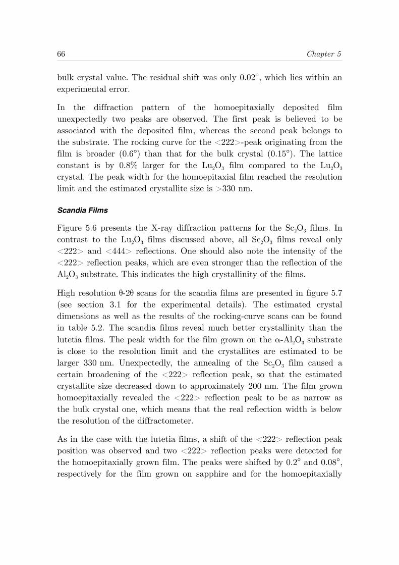
66 Chapter 5
bulk crystal value. The residual shift was only 0.02°, which lies within anexperimental error.
In the diffraction pattern of the homoepitaxially deposited filmunexpectedly two peaks are observed. The first peak is believed to beassociated with the deposited film, whereas the second peak belongs tothe substrate. The rocking curve for the <222>-peak originating from thefilm is broader (0.6°) than that for the bulk crystal (0.15°). The latticeconstant is by 0.8% larger for the Lu2O3 film compared to the Lu2O3
crystal. The peak width for the homoepitaxial film reached the resolutionlimit and the estimated crystallite size is >330 nm.
Scandia Films
Figure 5.6 presents the X-ray diffraction patterns for the Sc2O3 films. Incontrast to the Lu2O3 films discussed above, all Sc2O3 films reveal only<222> and <444> reflections. One should also note the intensity of the<222> reflection peaks, which are even stronger than the reflection of theAl2O3 substrate. This indicates the high crystallinity of the films.
High resolution θ-2θ scans for the scandia films are presented in figure 5.7(see section 3.1 for the experimental details). The estimated crystaldimensions as well as the results of the rocking-curve scans can be foundin table 5.2. The scandia films reveal much better crystallinity than thelutetia films. The peak width for the film grown on the α-Al2O3 substrateis close to the resolution limit and the crystallites are estimated to belarger 330 nm. Unexpectedly, the annealing of the Sc2O3 film caused acertain broadening of the <222> reflection peak, so that the estimatedcrystallite size decreased down to approximately 200 nm. The film grownhomoepitaxially revealed the <222> reflection peak to be as narrow asthe bulk crystal one, which means that the real reflection width is belowthe resolution of the diffractometer.
As in the case with the lutetia films, a shift of the <222> reflection peakposition was observed and two <222> reflection peaks were detected forthe homoepitaxially grown film. The peaks were shifted by 0.2° and 0.08°,respectively for the film grown on sapphire and for the homoepitaxially
X-ray Diffraction Analysis 67
grown film. This corresponds to about 0.6% and 0.25% lattice constantsincrease. Annealing did not influence the peak position and,correspondingly, the lattice constant in the case of scandia.
§5.4 Summary and Discussion
The X-ray diffraction analysis of the PLD-films presented in this chaptershowed, that the ytterbia, lutetia, and scandia films form a cubic latticetypical for these sesquioxides and the crystallites are preferably<111>-orientated.
Sc2O3 films have been proved to be highly textured in <111>-direction.Crystallites with the dimensions of several hundred nanometers have beenformed. In some case the resolution limit of the diffractometers have beenreached so that only the lower limit for the crystallite's size could beestimated.
Substantially smaller crystallites are formed in Yb2O3 films (up to~70 nm) and Lu2O3 films grown on sapphire substrates (up to ~50 nm).The Lu2O3 film grown homoepitaxially revealed crystallites in the range ofhundreds nanometers. Additionally, the lutetia films revealed crystalliteorientations other than <111>. Lu3+ and Yb3+ have higher mass comparedto Sc3+, which means, that at the same temperature Lu- and Yb-ions willhave lower mobilities in comparison with lighter Sc-ions. Thus, the highermobility of the Sc-ions on the substrate surface is believed to stimulatethe growth of larger crystallites. In case of the ytterbia films a higherlaser fluence was used during the deposition. Hence, higher kineticenergies of the plasma particles seem to compensate for the lack ofthermal energy of the ions.
In the upper layers of the 3.3 μm thick Lu2O3 film grown on α-Al2O3 the<111> orientation predefined by the substrate is apparently lost, due tothe substantially smaller size of crystallites compared to the film thicknessand, consequently, a high density of the grain boundaries. This wasevidenced by the presence in the XRD patterns of the diffraction peakscorresponding to other orientations. Perfect lattice matching in case ofhomoepitaxial growth initiates the formation of larger, strongly orientated
68 Chapter 5
crystallites, so that the orientation predefined by the substrate ispreserved at the film thickness of 3.5 μm.
The lattice constants for the PLD-films have been found to be slightlylarger compared to the bulk crystal values by up to 1.2% for Lu2O3 andup to 0.6% for Sc2O3. This effect may originate from the high kineticenergies of the ions in the plasma plume. The ions are not only depositedon the surface, but are also implanted into the already formed lattice anddisturb its structure. Due to the relatively low temperature during thedeposition (700°C) compared to the melting point (~2400°C), therecrystallization effect might be limited. After annealing at 900°C thelattice constant for the lutetia film was almost equal to the crystal value.In the case of the scandia films post annealing have no effect on thelattice constant. The increase of the lattice constant can also result fromthe relatively high concentration (4 mol.%) of the Yb3+-ions in Sc2O3
films, which are larger (0.87 Å) compared to the Sc3+-ions (0.75 Å).Whereas the radius of Lu3+ (0.86 Å) is almost equal to that of Yb3+. Thefact, that annealing do not influence the lattice constant of scandia films,confirms, that in this case the effect is most probably due to the dopant.
Yb-doped YAG films deposited on α-Al2O3 and YAG substrates at 700°Cdid not reveal any indications of a crystalline YAG structure. Onlyrandomly oriented YAG nanocrystallites have been formed after annealingof the samples at 1200°C. This correlates with the annealing experimentswith thin amorphous Eu:Y2O3 films on sapphire substrates [Bär05]. Thefilms showed typical Eu:Y2O3 emission spectra for annealing temperaturesup to 1000°C; above 1000°C emission lines assigned to Eu:YAG were alsodetected in the emission spectrum. On the other hand, Ezaki et al.[Eza96] reported crystalline growth of pulsed- laser-deposited YAG filmsstarting from 500°C substrate temperature. However, these films weredeposited under ultra-high vacuum conditions (~1×10⁻⁷ mbar). Alsogadolinium-gallium garnet (GGG) films, which have the same structurewith YAG, have been shown to grow in a crystalline form at relatively lowtemperatures of 650°C [Gri04b] (Nd:GGG) and up to 800°C [Lan05](Pr:GGG). In both reports relatively high oxygen pressures of 2-5×10⁻² mbar were used; however, the target-substrate distance was as short
X-ray Diffraction Analysis 69
as ~5 cm. It is believed, that the high kinetic energy of the plasmaparticles, due to low oxygen pressure or short working distance,contributed to the crystalline growth. Another reason, that can hinder thegrowth of crystalline YAG films in our case, is quite high concentration ofYb3+-ions (10 mol.%). Yb3+ has a different mass and ionic radiuscompared to Y3+, which can influence the YAG lattice formation.
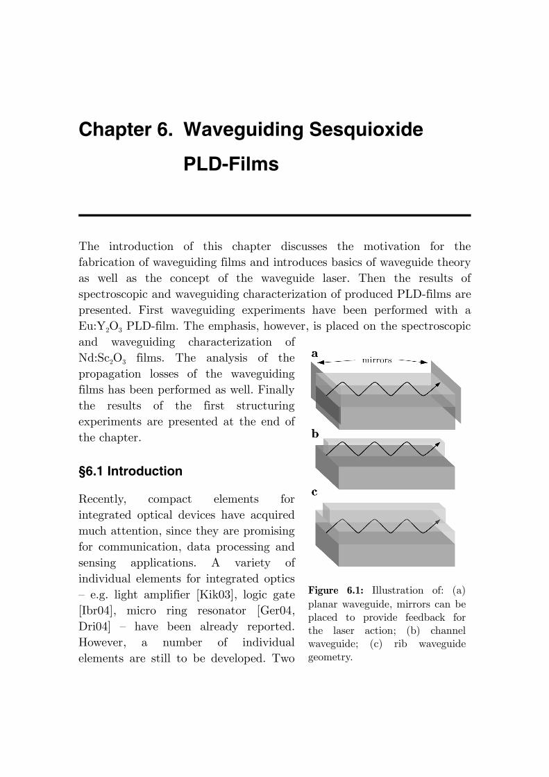
Chapter 6. Waveguiding Sesquioxide
PLD-Films
The introduction of this chapter discusses the motivation for thefabrication of waveguiding films and introduces basics of waveguide theoryas well as the concept of the waveguide laser. Then the results ofspectroscopic and waveguiding characterization of produced PLD-films arepresented. First waveguiding experiments have been performed with aEu:Y2O3 PLD-film. The emphasis, however, is placed on the spectroscopicand waveguiding characterization ofNd:Sc2O3 films. The analysis of thepropagation losses of the waveguidingfilms has been performed as well. Finallythe results of the first structuringexperiments are presented at the end ofthe chapter.
§6.1 Introduction
Recently, compact elements forintegrated optical devices have acquiredmuch attention, since they are promisingfor communication, data processing andsensing applications. A variety ofindividual elements for integrated optics– e.g. light amplifier [Kik03], logic gate[Ibr04], micro ring resonator [Ger04,Dri04] – have been already reported.However, a number of individualelements are still to be developed. Two
Figure 6.1: Illustration of: (a)planar waveguide, mirrors can beplaced to provide feedback forthe laser action; (b) channelwaveguide; (c) rib waveguidegeometry.
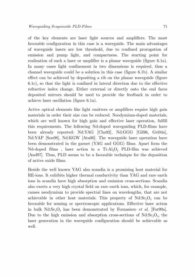
Waveguiding Sesquioxide PLD-Films 71
of the key elements are laser light sources and amplifiers. The mostfavorable configuration in this case is a waveguide. The main advantagesof waveguide lasers are low threshold, due to confined prorogation ofemission and pump light, and compactness. The starting point forrealization of such a laser or amplifier is a planar waveguide (figure 6.1a).In many cases light confinement in two dimensions is required, thus achannel waveguide could be a solution in this case (figure 6.1b). A similareffect can be achieved by depositing a rib on the planar waveguide (figure6.1c), so that the light is confined in lateral direction due to the effectiverefractive index change. Either external or directly onto the end facesdeposited mirrors should be used to provide the feedback in order toachieve laser oscillation (figure 6.1a).
Active optical elements like light emitters or amplifiers require high gainmaterials in order their size can be reduced. Neodymium-doped materials,which are well known for high gain and effective laser operation, fulfillthis requirements. The following Nd-doped waveguiding PLD-films havebeen already reported: Nd:YAG [Cha92], Nd:GGG [Gil96, Gri04a],Nd:YAP [Son98], Nd:KGW [Ata00]. The waveguide laser operation havebeen demonstrated in the garnet (YAG and GGG) films. Apart form theNd-doped films , laser action in a Ti:Al2O3 PLD-film was achieved[And97]. Thus, PLD seems to be a favorable technique for the depositionof active oxide films.
Beside the well known YAG also scandia is a promising host material forRE-ions. It exhibits higher thermal conductivity than YAG and rare earthions in scandia have high absorption and emission cross-sections. Scandiaalso exerts a very high crystal field on rare earth ions, which, for example,causes neodymium to provide spectral lines on wavelengths, that are notachievable in other host materials. This property of Nd:Sc2O3 can befavorable for sensing or spectroscopic applications. Effective laser actionin bulk Nd:Sc2O3 has been demonstrated by Fornasiero et al. [For99a].Due to the high emission and absorption cross-sections of Nd:Sc2O3, thelaser generation in the waveguide configuration should be achievable aswell.
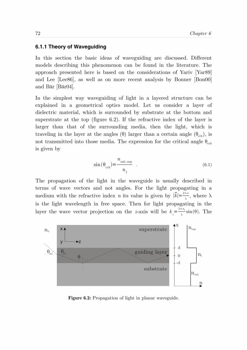
72 Chapter 6
6.1.1 Theory of Waveguiding
In this section the basic ideas of waveguiding are discussed. Differentmodels describing this phenomenon can be found in the literature. Theapproach presented here is based on the considerations of Yariv [Yar89]and Lee [Lee86], as well as on more recent analysis by Bonner [Bon00]and Bär [Bär04].
In the simplest way waveguiding of light in a layered structure can beexplained in a geometrical optics model. Let us consider a layer ofdielectric material, which is surrounded by substrate at the bottom andsuperstrate at the top (figure 6.2). If the refractive index of the layer islarger than that of the surrounding media, then the light, which istraveling in the layer at the angles (θ) larger than a certain angle (θcrit), isnot transmitted into those media. The expression for the critical angle θcrit
is given by
sin θcrit
=n
sub ,sup
nf
. (6.1)
The propagation of the light in the waveguide is usually described interms of wave vectors and not angles. For the light propagating in amedium with the refractive index n its value is given by ∣k∣=
2πn
λ, where λ
is the light wavelength in free space. Then for light propagating in thelayer the wave vector projection on the z-axis will be k
z=
2πn f
λsinθ. The
Figure 6.2: Propagation of light in planar waveguide.
θinθ
θtr nf
nsub
z
x
y
n0
d
0
-d
n
nsupx
superstrate
guiding layer
substrate
Waveguiding Sesquioxide PLD-Films 73
quantity n f sin θ is often denoted as the effective refractive index neff. Theguidance condition θ>θcrit is satisfied, if neff>nsub,sup.
The restriction for the coupling angles (θin), which result in guiding oflight can also be derived from the guidance condition θ>θcrit
n0sin θ
inn
f
2nsub ,sup
2 . (6.2)
The quantity n0sin θ
in
max is more convenient from the experimental pointof view and is referred to as numerical aperture of the waveguide (NA).
However, the geometric optics model cannot give the accurateconsideration of all effects. Thus, for example, a discrete number of guidedmodes can not be explained. The correct treatment of the subject can bederived from Maxwell's equations
∇× E r ,t =∂ B r ,t
∂ t(6.3)
∇× H r ,t =∂ D r ,t
∂ tj r ,t (6.4)
∇⋅D r ,t =ρr ,t (6.5)
∇⋅B r ,t =0 , (6.6)
where E and B are the electric and magnetic fields respectively, D is theelectric displacement vector, H is the magnetic flux density, ρ and j arecharge and current densities, respectively. In the case of isotropicdielectric media (ρ=0, j =0, D=ε E, B=μ H) the equation for E is givenby
∇2 E=n2
c2
∂2 E
∂ t 2, (6.7)
which is termed the wave equation. The solution for equation 6.7 can bepresented in the following form
E x ,y ,z ,t =E x ,y ,z e iωt . (6.8)
74 Chapter 6
Due to translation symmetry along the y-axis (∂ E
∂y=0) in the case of a
planar waveguide (as presented in figure 6.2), this general solution splitsinto two groups: (1) Ez=Ex=Hy=0 (E is transversal to the incidenceplane), referred to as TE-modes; (2) Hz=Hx=Ey=0 ( H is transversal to theincidence plane), referred to as TM-modes.
In the following consideration, only transversal electrical (TE) modes areconsidered, the transversal magnetic modes can be treated analogously. Inthe case of a planar waveguide the solution for the TE-modes can bewritten as
Eyx ,y ,z ,t =E
yx e
i ωtkzz
. (6.9)
In order for the light to be guided, the solutions should be oscillating inthe guiding layer and decaying in the substrate and superstrate. So wesearch solutions in the following form
Ey={E sup
eα
supx
,x d
Efcos k
xx ψ ,dx d
Esub
eαsubx ,x d
, (6.10)
where Esup,sub,f are the electric field amplitudes in the correspondingregions, ψ is the phase shift, αsup,sub and kx are the wavenumbers, whichare derived from the solution of the wave equation 6.7 and are given by
αsup
=k neff
2n
sup
2
kx=k n
f
2n
eff
2
αsub=k n eff
2n sub
2 .
(6.11)
From the continuity condition ∂E
y
∂x=0 at the interfaces x=±d, one can
eliminate the phase ψ and the following equation can be obtained
2kxdarctan
αsup
k x
arctanα
sub
k x
=p π . (6.12)
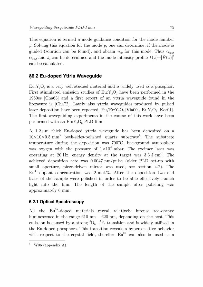
Waveguiding Sesquioxide PLD-Films 75
This equation is termed a mode guidance condition for the mode numberp. Solving this equation for the mode p, one can determine, if the mode isguided (solution can be found), and obtain neff for this mode. Thus αsup,αsub, and kx can be determined and the mode intensity profile I x =∣E x ∣2
can be calculated.
§6.2 Eu-doped Yttria Waveguide
Eu:Y2O3 is a very well studied material and is widely used as a phosphor.First stimulated emission studies of Eu:Y2O3 have been performed in the1960es [Cha63] and a first report of an yttria waveguide found in theliterature is [Cha72]. Lately also yttria waveguides produced by pulsedlaser deposition have been reported: Eu/Er:Y2O3 [Via00], Er:Y2O3 [Kor01].The first waveguiding experiments in the course of this work have beenperformed with an Eu:Y2O3 PLD-film.
A 1.2 μm thick Eu-doped yttria waveguide has been deposited on a10×10×0.5 mm3 both-sides-polished quartz substrate1. The substratetemperature during the deposition was 700°C, background atmospherewas oxygen with the pressure of 1 ×10⁻² mbar. The excimer laser wasoperating at 20 Hz, energy density at the target was 3.3 J⋅cm-2. Theachieved deposition rate was 0.0047 nm/pulse (older PLD set-up withsmall aperture, piezo-driven mirror was used, see section 4.2). TheEu3+-dopant concentration was 2 mol.%. After the deposition two endfaces of the sample were polished in order to be able effectively launchlight into the film. The length of the sample after polishing wasapproximately 6 mm.
6.2.1 Optical Spectroscopy
All the Eu3+-doped materials reveal relatively intense red-orangeluminescence in the range 610 nm – 620 nm, depending on the host. Thisemission is caused by a strong 5D0→
7F2 transition and is widely utilized inthe Eu-doped phosphors. This transition reveals a hypersensitive behaviorwith respect to the crystal field, therefore Eu3+ can also be used as a
1 W06 (appendix A).
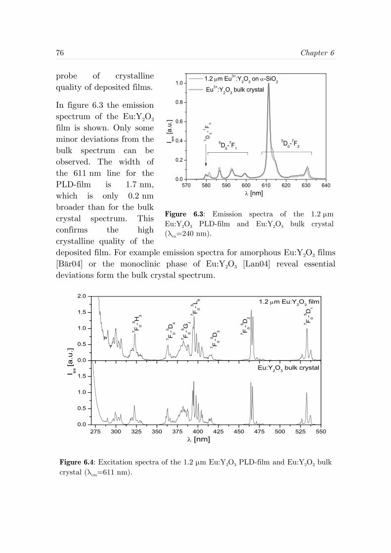
76 Chapter 6
probe of crystallinequality of deposited films.
In figure 6.3 the emissionspectrum of the Eu:Y2O3
film is shown. Only someminor deviations from thebulk spectrum can beobserved. The width ofthe 611 nm line for thePLD-film is 1.7 nm,which is only 0.2 nmbroader than for the bulkcrystal spectrum. Thisconfirms the highcrystalline quality of thedeposited film. For example emission spectra for amorphous Eu:Y2O3 films[Bär04] or the monoclinic phase of Eu:Y2O3 [Lan04] reveal essentialdeviations form the bulk crystal spectrum.
Figure 6.3: Emission spectra of the 1.2 μmEu:Y2O3 PLD-film and Eu:Y2O3 bulk crystal(λex=240 nm).
570 580 590 600 610 620 630 6400.0
0.2
0.4
0.6
0.8
1.0
5D0-7F2
5D0-7F1
I em [a
.u.]
λ [nm]
1.2 μm Eu3+:Y2O3 on α-SiO2
Eu3+:Y2O3 bulk crystal
5D
0-7F
0
Figure 6.4: Excitation spectra of the 1.2 μm Eu:Y2O3 PLD-film and Eu:Y2O3 bulkcrystal (λem=611 nm).
275 300 325 350 375 400 425 450 475 500 525 5500.0
0.5
1.0
1.5I ex [
a.u
.]
λ [nm]
1.2 μm Eu:Y2O3 film
0.0
0.5
1.0
1.5
2.07 F 0-5 D
1
7 F 0-5 D2
7 F 0-5 D3
7 F 0-5 L 6
7 F 0-5 GJ
7 F 0-5 D4
Eu:Y2O3 bulk crystal
7 F 0-5 H3
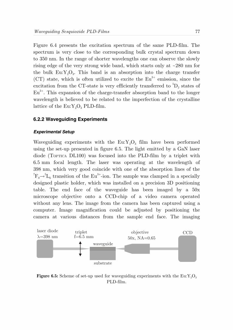
Waveguiding Sesquioxide PLD-Films 77
Figure 6.4 presents the excitation spectrum of the same PLD-film. Thespectrum is very close to the corresponding bulk crystal spectrum downto 350 nm. In the range of shorter wavelengths one can observe the slowlyrising edge of the very strong wide band, which starts only at ~280 nm forthe bulk Eu:Y2O3. This band is an absorption into the charge transfer(CT) state, which is often utilized to excite the Eu3+ emission, since theexcitation from the CT-state is very efficiently transferred to 5DJ states ofEu3+. This expansion of the charge-transfer absorption band to the longerwavelength is believed to be related to the imperfection of the crystallinelattice of the Eu:Y2O3 PLD-film.
6.2.2 Waveguiding Experiments
Experimental Setup
Waveguiding experiments with the Eu:Y2O3 film have been performedusing the set-up presented in figure 6.5. The light emitted by a GaN laserdiode (TOPTICA DL100) was focused into the PLD-film by a triplet with6.5 mm focal length. The laser was operating at the wavelength of398 nm, which very good coincide with one of the absorption lines of the7F0→
5L6 transition of the Eu3+-ion. The sample was clamped in a speciallydesigned plastic holder, which was installed on a precision 3D positioningtable. The end face of the waveguide has been imaged by a 50xmicroscope objective onto a CCD-chip of a video camera operatedwithout any lens. The image from the camera has been captured using acomputer. Image magnification could be adjusted by positioning thecamera at various distances from the sample end face. The imaging
Figure 6.5: Scheme of set-up used for waveguiding experiments with the Eu:Y2O3
PLD-film.
CCD
waveguide
substrate
50x, NA=0.65
laser diode tripletf=6.5 mmλ=398 nm
objective
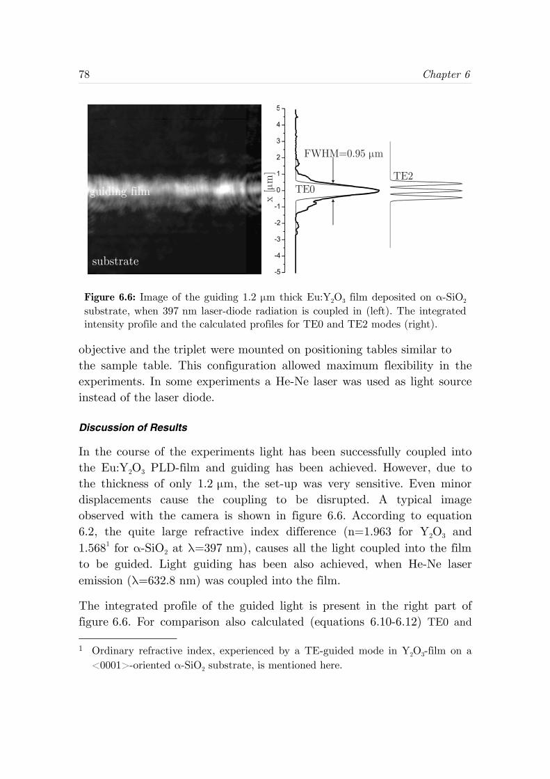
78 Chapter 6
objective and the triplet were mounted on positioning tables similar tothe sample table. This configuration allowed maximum flexibility in theexperiments. In some experiments a He-Ne laser was used as light sourceinstead of the laser diode.
Discussion of Results
In the course of the experiments light has been successfully coupled intothe Eu:Y2O3 PLD-film and guiding has been achieved. However, due tothe thickness of only 1.2 μm, the set-up was very sensitive. Even minordisplacements cause the coupling to be disrupted. A typical imageobserved with the camera is shown in figure 6.6. According to equation6.2, the quite large refractive index difference (n=1.963 for Y2O3 and1.5681 for α-SiO2 at λ=397 nm), causes all the light coupled into the filmto be guided. Light guiding has been also achieved, when He-Ne laseremission (λ=632.8 nm) was coupled into the film.
The integrated profile of the guided light is present in the right part offigure 6.6. For comparison also calculated (equations 6.10-6.12) TE0 and
1 Ordinary refractive index, experienced by a TE-guided mode in Y2O3-film on a<0001>-oriented α-SiO2 substrate, is mentioned here.
Figure 6.6: Image of the guiding 1.2 μm thick Eu:Y2O3 film deposited on α-SiO2
substrate, when 397 nm laser-diode radiation is coupled in (left). The integratedintensity profile and the calculated profiles for TE0 and TE2 modes (right).
guiding film
substratex
[μm
]-5
-4
-3
-2
-1
0
1
2
3
4
5
TE2TE0
FWHM=0.95 μm
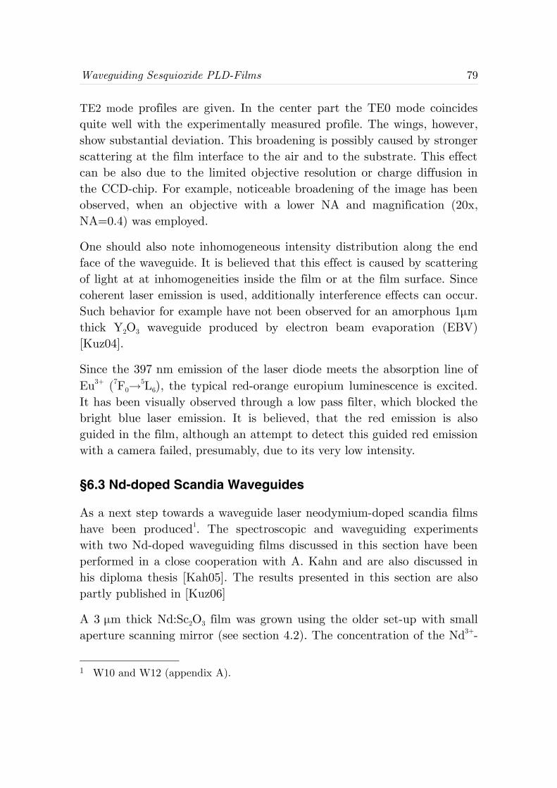
Waveguiding Sesquioxide PLD-Films 79
TE2 mode profiles are given. In the center part the TE0 mode coincidesquite well with the experimentally measured profile. The wings, however,show substantial deviation. This broadening is possibly caused by strongerscattering at the film interface to the air and to the substrate. This effectcan be also due to the limited objective resolution or charge diffusion inthe CCD-chip. For example, noticeable broadening of the image has beenobserved, when an objective with a lower NA and magnification (20x,NA=0.4) was employed.
One should also note inhomogeneous intensity distribution along the endface of the waveguide. It is believed that this effect is caused by scatteringof light at at inhomogeneities inside the film or at the film surface. Sincecoherent laser emission is used, additionally interference effects can occur.Such behavior for example have not been observed for an amorphous 1μmthick Y2O3 waveguide produced by electron beam evaporation (EBV)[Kuz04].
Since the 397 nm emission of the laser diode meets the absorption line ofEu3+ (7F0→
5L6), the typical red-orange europium luminescence is excited.It has been visually observed through a low pass filter, which blocked thebright blue laser emission. It is believed, that the red emission is alsoguided in the film, although an attempt to detect this guided red emissionwith a camera failed, presumably, due to its very low intensity.
§6.3 Nd-doped Scandia Waveguides
As a next step towards a waveguide laser neodymium-doped scandia filmshave been produced1. The spectroscopic and waveguiding experimentswith two Nd-doped waveguiding films discussed in this section have beenperformed in a close cooperation with A. Kahn and are also discussed inhis diploma thesis [Kah05]. The results presented in this section are alsopartly published in [Kuz06]
A 3 μm thick Nd:Sc2O3 film was grown using the older set-up with smallaperture scanning mirror (see section 4.2). The concentration of the Nd3+-
1 W10 and W12 (appendix A).
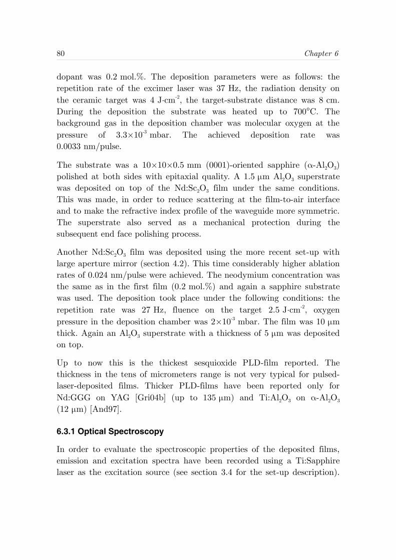
80 Chapter 6
dopant was 0.2 mol.%. The deposition parameters were as follows: therepetition rate of the excimer laser was 37 Hz, the radiation density onthe ceramic target was 4 J⋅cm-2, the target-substrate distance was 8 cm.During the deposition the substrate was heated up to 700°C. Thebackground gas in the deposition chamber was molecular oxygen at thepressure of 3.3×10⁻³ mbar. The achieved deposition rate was0.0033 nm/pulse.
The substrate was a 10×10×0.5 mm (0001)-oriented sapphire (α-Al2O3)polished at both sides with epitaxial quality. A 1.5 μm Al2O3 superstratewas deposited on top of the Nd:Sc2O3 film under the same conditions.This was made, in order to reduce scattering at the film-to-air interfaceand to make the refractive index profile of the waveguide more symmetric.The superstrate also served as a mechanical protection during thesubsequent end face polishing process.
Another Nd:Sc2O3 film was deposited using the more recent set-up withlarge aperture mirror (section 4.2). This time considerably higher ablationrates of 0.024 nm/pulse were achieved. The neodymium concentration wasthe same as in the first film (0.2 mol.%) and again a sapphire substratewas used. The deposition took place under the following conditions: therepetition rate was 27 Hz, fluence on the target 2.5 J⋅cm-2, oxygenpressure in the deposition chamber was 2×10⁻³ mbar. The film was 10 μmthick. Again an Al2O3 superstrate with a thickness of 5 μm was depositedon top.
Up to now this is the thickest sesquioxide PLD-film reported. Thethickness in the tens of micrometers range is not very typical for pulsed-laser-deposited films. Thicker PLD-films have been reported only forNd:GGG on YAG [Gri04b] (up to 135 μm) and Ti:Al2O3 on α-Al2O3
(12 μm) [And97].
6.3.1 Optical Spectroscopy
In order to evaluate the spectroscopic properties of the deposited films,emission and excitation spectra have been recorded using a Ti:Sapphirelaser as the excitation source (see section 3.4 for the set-up description).
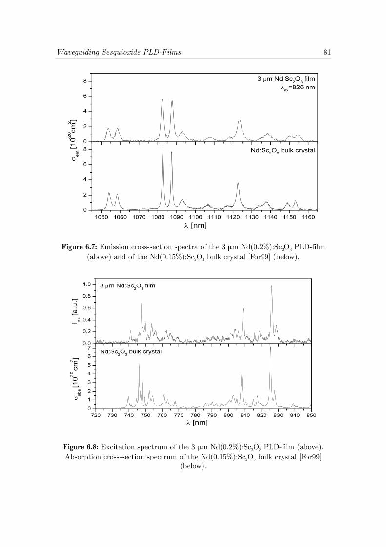
Waveguiding Sesquioxide PLD-Films 81
Figure 6.7: Emission cross-section spectra of the 3 μm Nd(0.2%):Sc2O3 PLD-film(above) and of the Nd(0.15%):Sc2O3 bulk crystal [For99] (below).
Figure 6.8: Excitation spectrum of the 3 μm Nd(0.2%):Sc2O3 PLD-film (above).Absorption cross-section spectrum of the Nd(0.15%):Sc2O3 bulk crystal [For99]
(below).
1050 1060 1070 1080 1090 1100 1110 1120 1130 1140 1150 11600
2
4
6
8
σe
m [
10-2
0 cm2 ]
λ [nm]
λex=826 nm
0
2
4
6
8 3 μm Nd:Sc2O3 film
Nd:Sc2O3 bulk crystal
0.0
0.2
0.4
0.6
0.8
1.0
I ex [a
.u.]
720 730 740 750 760 770 780 790 800 810 820 830 840 8500
1
2
3
4
5
6
7
λ [nm]
3 μm Nd:Sc2O3 film
σa
bs [1
0-20 c
m2 ]
Nd:Sc2O3 bulk crystal
82 Chapter 6
Figure 6.7 shows the spectrum of the stimulated emission cross-section forthe 4F3/2→
4I11/2(Nd3+) transition (λex=826 nm), calculated using theFüchtbauer-Ladenburg equation 3.16 (βij=0.445 and τ=303 μs used). Thistransition is most often utilized for laser action in Nd-based materials,and in the case of the scandia lasing can be achieved either at 1082 nm orat 1087 nm. However laser operation was also demonstrated for the4F3/2→
4I9/2 transition at 966 nm and for the 4F3/2→4I13/2 transition at
1486 nm [For99, For99a].
The emission spectrum of the Nd:Sc2O3 film resembles the one of the bulkcrystal closely. However, some broadening is observed, which leads to thefact, that the peak cross-section values are only about 68% of thecorresponding bulk values.
It was not possible to measure an absorption spectrum of Nd-dopants byconventional methods. The signal was too weak due to the quite low Nd3+
concentration in the film. Therefore the excitation spectrum(λem=1082 nm) in the range of 720-850 nm has been measured for the3 μm thick Nd:Sc2O3 film (figure 6.8), in order to estimate the bestwavelength for pumping. The 826 nm line is the most beneficial and couldbe used for pumping with a Ti:Sapphire laser, but also the 808 nm line,where commercial laser diodes are available, can be utilized. The spectrafor the 10 μm Nd:Sc2O3 PLD-film are almost identical to the onespresented in figures 6.7 and 6.8 for the 3 μm Nd:Sc2O3 film.
6.3.2 Lifetime Measurements
The luminescence decay curves for the 4F3/2→4I9/2 transition (966 nm) of
Nd3+ in the 3 μm Nd:Sc2O3 film and in the ceramic target used as areference are presented in figure 6.9. The excitation wavelength was826 nm. The measurements have been done at the set-up described insection 3.4. It can be seen that the decay has a nonexponential behavior.This is caused by nonlinear processes (up-conversion, cross-relaxation andenergy migration) taking place in spite of the low neodymiumconcentration. A similar effect was observed by Fornasiero forneodymium-doped bulk sesquioxide crystals [For99]. Therefore only thelater part of the decay curve (t→∞) was used to estimate the exponential
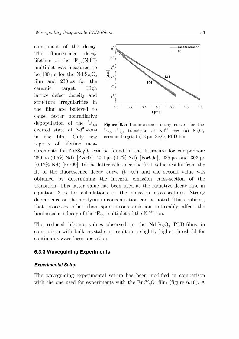
Waveguiding Sesquioxide PLD-Films 83
component of the decay.The fluorescence decaylifetime of the 4F3/2(Nd3+)multiplet was measured tobe 180 μs for the Nd:Sc2O3
film and 230 μs for theceramic target. Highlattice defect density andstructure irregularities inthe film are believed tocause faster nonradiativedepopulation of the 4F3/2
excited state of Nd3+-ionsin the film. Only fewreports of lifetime mea-surements for Nd:Sc2O3 can be found in the literature for comparison:260 μs (0.5% Nd) [Zve67], 224 μs (0.7% Nd) [For99a], 285 μs and 303 μs(0.12% Nd) [For99]. In the latter reference the first value results from thefit of the fluorescence decay curve (t→∞) and the second value wasobtained by determining the integral emission cross-section of thetransition. This latter value has been used as the radiative decay rate inequation 3.16 for calculations of the emission cross-sections. Strongdependence on the neodymium concentration can be noted. This confirms,that processes other than spontaneous emission noticeably affect theluminescence decay of the 4F3/2 multiplet of the Nd3+-ion.
The reduced lifetime values observed in the Nd:Sc2O3 PLD-films incomparison with bulk crystal can result in a slightly higher threshold forcontinuous-wave laser operation.
6.3.3 Waveguiding Experiments
Experimental Setup
The waveguiding experimental set-up has been modified in comparisonwith the one used for experiments with the Eu:Y2O3 film (figure 6.10). A
Figure 6.9: Luminescence decay curves for the4F3/2→
4I9/2 transition of Nd3+ for: (a) Sc2O3
ceramic target; (b) 3 μm Sc2O3 PLD-film.
0.0 0.2 0.4 0.6 0.8 1.0 1.2
e-5
e-4
e-3
e-2
e-1
e0 measurement fit
(b)
I [a.
u.]
t [ms]
(a)
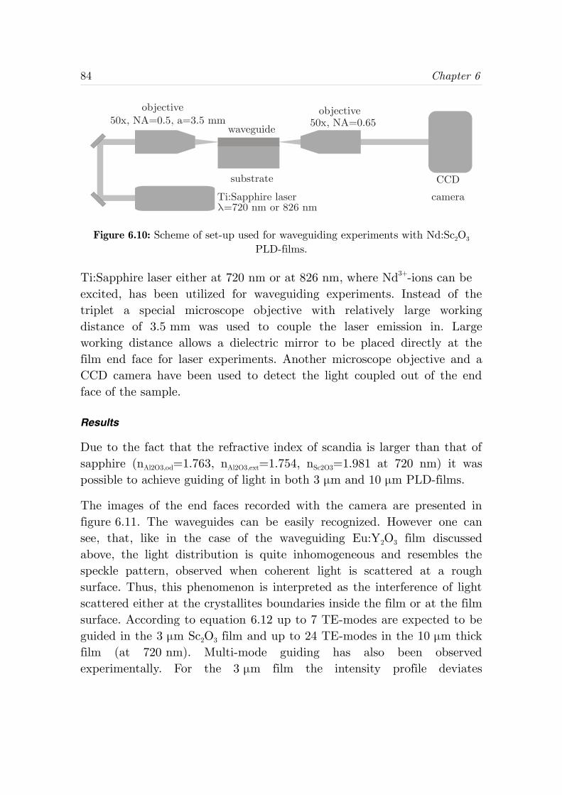
84 Chapter 6
Ti:Sapphire laser either at 720 nm or at 826 nm, where Nd3+-ions can beexcited, has been utilized for waveguiding experiments. Instead of thetriplet a special microscope objective with relatively large workingdistance of 3.5 mm was used to couple the laser emission in. Largeworking distance allows a dielectric mirror to be placed directly at thefilm end face for laser experiments. Another microscope objective and aCCD camera have been used to detect the light coupled out of the endface of the sample.
Results
Due to the fact that the refractive index of scandia is larger than that ofsapphire (nAl2O3,od=1.763, nAl2O3,ext=1.754, nSc2O3=1.981 at 720 nm) it waspossible to achieve guiding of light in both 3 μm and 10 μm PLD-films.
The images of the end faces recorded with the camera are presented infigure 6.11. The waveguides can be easily recognized. However one cansee, that, like in the case of the waveguiding Eu:Y2O3 film discussedabove, the light distribution is quite inhomogeneous and resembles thespeckle pattern, observed when coherent light is scattered at a roughsurface. Thus, this phenomenon is interpreted as the interference of lightscattered either at the crystallites boundaries inside the film or at the filmsurface. According to equation 6.12 up to 7 TE-modes are expected to beguided in the 3 μm Sc2O3 film and up to 24 TE-modes in the 10 μm thickfilm (at 720 nm). Multi-mode guiding has also been observedexperimentally. For the 3 μm film the intensity profile deviates
Figure 6.10: Scheme of set-up used for waveguiding experiments with Nd:Sc2O3
PLD-films.
waveguide
substrate
50x, NA=0.65
Ti:Sapphire laser
objective
λ=720 nm or 826 nm
objective
CCD
50x, NA=0.5, a=3.5 mm
camera
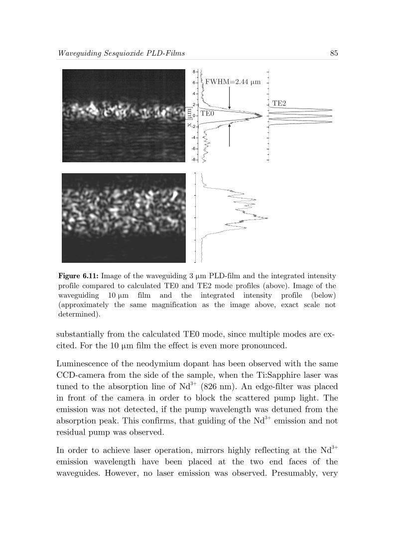
Waveguiding Sesquioxide PLD-Films 85
substantially from the calculated TE0 mode, since multiple modes are ex-cited. For the 10 μm film the effect is even more pronounced.
Luminescence of the neodymium dopant has been observed with the sameCCD-camera from the side of the sample, when the Ti:Sapphire laser wastuned to the absorption line of Nd3+ (826 nm). An edge-filter was placedin front of the camera in order to block the scattered pump light. Theemission was not detected, if the pump wavelength was detuned from theabsorption peak. This confirms, that guiding of the Nd3+ emission and notresidual pump was observed.
In order to achieve laser operation, mirrors highly reflecting at the Nd3+
emission wavelength have been placed at the two end faces of thewaveguides. However, no laser emission was observed. Presumably, very
Figure 6.11: Image of the waveguiding 3 μm PLD-film and the integrated intensityprofile compared to calculated TE0 and TE2 mode profiles (above). Image of thewaveguiding 10 μm film and the integrated intensity profile (below)(approximately the same magnification as the image above, exact scale notdetermined).
TE0
FWHM=2.44 μm
TE2
x [μ
m]
86 Chapter 6
high losses in the waveguides (as discussed below) hinder the laseroperation. Thus, further optimization of the deposition process is stillrequired to fabricate films with lower propagation losses.
6.3.4 Propagation Losses
In order for the laser operation to be achieved in a waveguide laser, thegain in the waveguide must compensate for losses, which can be separatedinto two groups: (a) coupling losses, which result from the finitetransmission coefficient of resonator mirrors and imperfect coupling fromand into the waveguide; (b) propagations losses, resulting from scatteringand absorption in the medium itself. Whereas the former depends mostlyon the laser cavity design and geometry, the latter to a greater extentdepends on the properties of the waveguide itself. Thus, the propagationloss of the waveguide is one of the most important parameters, if laseroperation is considered.
Since Sc2O3 is fully transparent in the visible and near infrared spectralrange, the absorption for the Nd:Sc2O3 waveguides discussed here isdetermined only by absorption of the dopant and therefore easy tocontrol. The scattering losses on the contrary are difficult to measure andtheir origin is often not obvious.
The standard technique for measurements of propagation losses in fibersis to shorten the fiber step-by-step and to measure the intensity of thetransmitted light for each fiber length. However, since this is a destructivetechnique, it has not found wide application in the waveguide field. Incase laser operation in the waveguide is achieved, the Findlay-Claymethod [Fin66] based on the analysis of lasing characteristics can beapplied. In the case of non-lasing waveguides the usual way is to observethe intensity of the guided or scattered light along the propagationdirection.
For both 3 μm and 10 μm thick Nd:Sc2O3 waveguides the scatteringpropagation losses have been determined in the following way: theradiation of a Ti:Sapphire laser was coupled into the waveguide(λ=826 nm) and the decrease of the excited Nd3+ luminescence along the
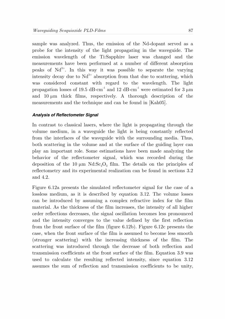
Waveguiding Sesquioxide PLD-Films 87
sample was analyzed. Thus, the emission of the Nd-dopant served as aprobe for the intensity of the light propagating in the waveguide. Theemission wavelength of the Ti:Sapphire laser was changed and themeasurements have been performed at a number of different absorptionpeaks of Nd3+. In this way it was possible to separate the varyingintensity decay due to Nd3+ absorption from that due to scattering, whichwas considered constant with regard to the wavelength. The lightpropagation losses of 19.5 dB·cm-1 and 12 dB·cm-1 were estimated for 3 μmand 10 μm thick films, respectively. A thorough description of themeasurements and the technique and can be found in [Kah05].
Analysis of Reflectometer Signal
In contrast to classical lasers, where the light is propagating through thevolume medium, in a waveguide the light is being constantly reflectedfrom the interfaces of the waveguide with the surrounding media. Thus,both scattering in the volume and at the surface of the guiding layer canplay an important role. Some estimations have been made analyzing thebehavior of the reflectometer signal, which was recorded during thedeposition of the 10 μm Nd:Sc2O3 film. The details on the principles ofreflectometry and its experimental realization can be found in sections 3.2and 4.2.
Figure 6.12a presents the simulated reflectometer signal for the case of alossless medium, as it is described by equation 3.12. The volume lossescan be introduced by assuming a complex refractive index for the filmmaterial. As the thickness of the film increases, the intensity of all higherorder reflections decreases, the signal oscillation becomes less pronouncedand the intensity converges to the value defined by the first reflectionfrom the front surface of the film (figure 6.12b). Figure 6.12c presents thecase, when the front surface of the film is assumed to become less smooth(stronger scattering) with the increasing thickness of the film. Thescattering was introduced through the decrease of both reflection andtransmission coefficients at the front surface of the film. Equation 3.9 wasused to calculate the resulting reflected intensity, since equation 3.12assumes the sum of reflection and transmission coefficients to be unity,
88 Chapter 6
which is not the case here.The first five terms of theinfinite series were used,which was proven to providesufficient precision. In thismodel the reflection andtransmission coefficientswere assumed to decreaselinearly with the increasingfilm thickness. The modelwith the surface-relatedlosses was found to reflectthe behavior of theexperimental result (figure6.12d) more adequately. Asimilar reflectometer signalbehavior was observedduring the deposition of the3 μm waveguide.
Thus, presumably thescattering effects at thesurface seem to play themajor role for the Nd:Sc2O3
waveguides discussed here.A possible reason is scattering at the crystallite boundaries, howevermeasurements in the integrating sphere (section 3.3) have not revealedany dependency of the scattered light intensity on the crystallitedimensions. It is believed, that droplets and particulates at the surface ofthe film can cause the scattering of the light. Apart from the depositionparameters, like laser fluence or gas pressure, which can influence theparticulate density, one of the critical points can be the use of ceramictargets for the deposition. Since a ceramic is not completely dense,particulates in the micrometer range can be torn out during the ablationand adhere at the substrate without being evaporated. Even if a bulkcrystal is used as the target, additional steps, like surface polishing, can
Figure 6.12: Simulated reflectometer signalcurves for: (a) “no losses” model; (b) scatteringin film volume; (c) scattering at film surface.(d) Reflectometer signal recordedexperimentally during deposition of the 10 μmNd:Sc2O3 PLD-film.
0 1 2 3 4 5 6 7 8 9 100.2
0.3
0.4
0.5
I refle
c [V]
d [mm]
0
2
4
6
8
100
2
4
6
8
10
R [%
]
0
2
4
6
8
10
d
c
a
"surface loss" simulation
measured reflectometer signal
"no loss" simulation
"volume loss" simulation b
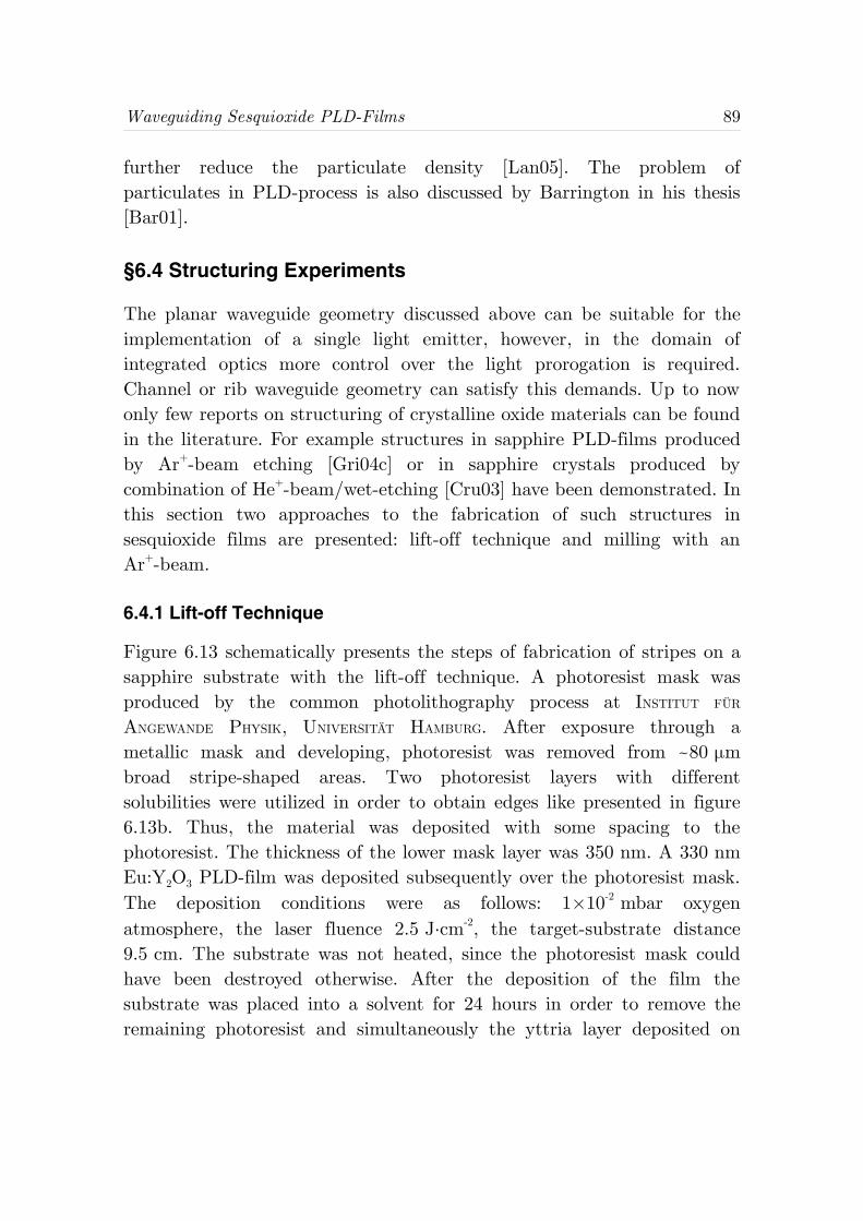
Waveguiding Sesquioxide PLD-Films 89
further reduce the particulate density [Lan05]. The problem ofparticulates in PLD-process is also discussed by Barrington in his thesis[Bar01].
§6.4 Structuring Experiments
The planar waveguide geometry discussed above can be suitable for theimplementation of a single light emitter, however, in the domain ofintegrated optics more control over the light prorogation is required.Channel or rib waveguide geometry can satisfy this demands. Up to nowonly few reports on structuring of crystalline oxide materials can be foundin the literature. For example structures in sapphire PLD-films producedby Ar+-beam etching [Gri04c] or in sapphire crystals produced bycombination of He+-beam/wet-etching [Cru03] have been demonstrated. Inthis section two approaches to the fabrication of such structures insesquioxide films are presented: lift-off technique and milling with anAr+-beam.
6.4.1 Lift-off Technique
Figure 6.13 schematically presents the steps of fabrication of stripes on asapphire substrate with the lift-off technique. A photoresist mask wasproduced by the common photolithography process at INSTITUT FÜR
ANGEWANDE PHYSIK, UNIVERSITÄT HAMBURG. After exposure through ametallic mask and developing, photoresist was removed from ~80 μmbroad stripe-shaped areas. Two photoresist layers with differentsolubilities were utilized in order to obtain edges like presented in figure6.13b. Thus, the material was deposited with some spacing to thephotoresist. The thickness of the lower mask layer was 350 nm. A 330 nmEu:Y2O3 PLD-film was deposited subsequently over the photoresist mask.The deposition conditions were as follows: 1×10⁻² mbar oxygenatmosphere, the laser fluence 2.5 J⋅cm-2, the target-substrate distance9.5 cm. The substrate was not heated, since the photoresist mask couldhave been destroyed otherwise. After the deposition of the film thesubstrate was placed into a solvent for 24 hours in order to remove theremaining photoresist and simultaneously the yttria layer deposited on
90 Chapter 6
Figure 6.13: Scheme of the lift-offtechnique: (a) two layers of photoresistare deposited; (b) photoresist isexposed through a mask and developed;(c) Y2O3 is deposited by PLD process;(d) photoresist is removed togetherwith Y2O3 on it.
Figure 6.14: Scheme of the Ar+-beametching process: (a) Y2O3 PLD-film isdeposited, (b) photoresist is depositedon top; (c) photoresist is exposedthrough a mask and developed; (d)Y2O3 is etched with Ar+-beam; (e)photoresist is removed.
Figure 6.15: SEM image of theEu:Y2O3 stripes on sapphire substrateproduced by the lift-off technique.
Figure 6.16: SEM image of step in theEu:Y2O3 PLD-film produced byAr+-beam etching.
a
b
c
d
b
c
d
e
a
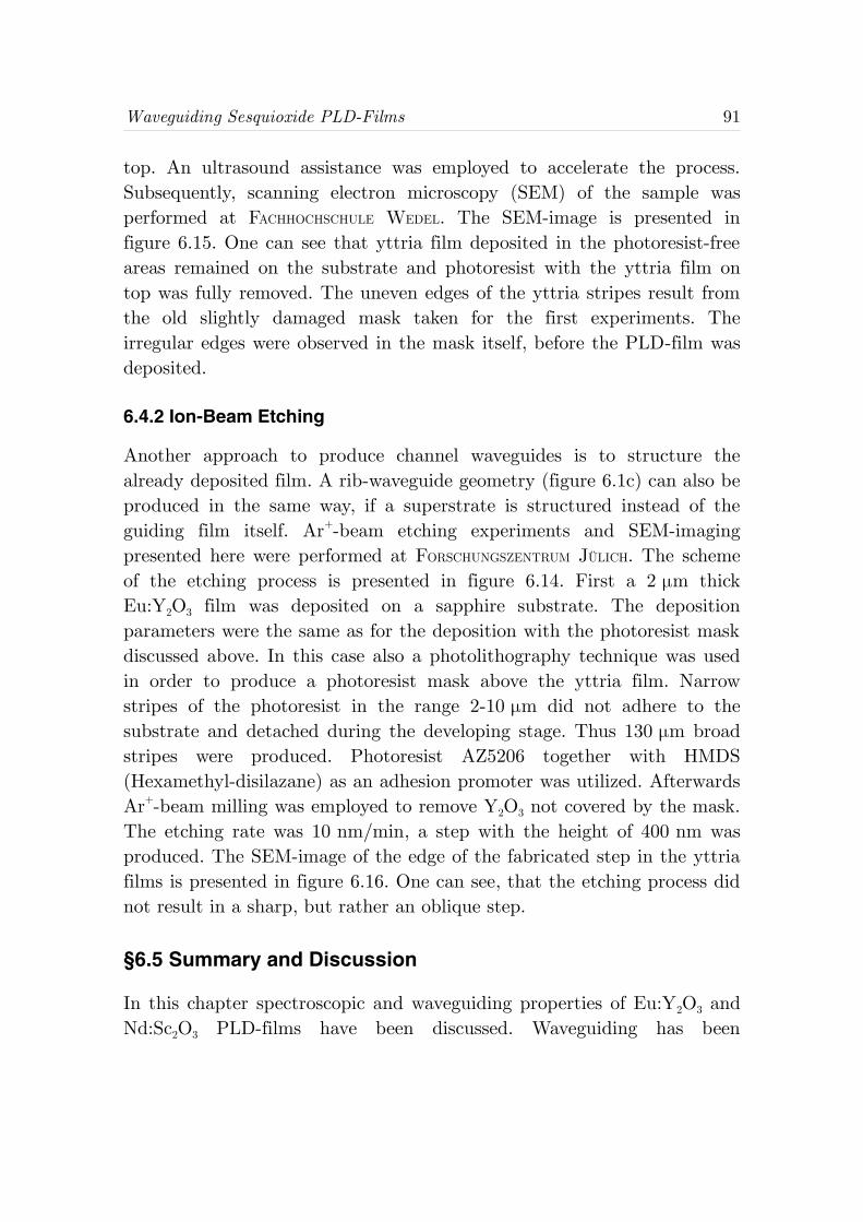
Waveguiding Sesquioxide PLD-Films 91
top. An ultrasound assistance was employed to accelerate the process.Subsequently, scanning electron microscopy (SEM) of the sample wasperformed at FACHHOCHSCHULE WEDEL. The SEM-image is presented infigure 6.15. One can see that yttria film deposited in the photoresist-freeareas remained on the substrate and photoresist with the yttria film ontop was fully removed. The uneven edges of the yttria stripes result fromthe old slightly damaged mask taken for the first experiments. Theirregular edges were observed in the mask itself, before the PLD-film wasdeposited.
6.4.2 Ion-Beam Etching
Another approach to produce channel waveguides is to structure thealready deposited film. A rib-waveguide geometry (figure 6.1c) can also beproduced in the same way, if a superstrate is structured instead of theguiding film itself. Ar+-beam etching experiments and SEM-imagingpresented here were performed at FORSCHUNGSZENTRUM JÜLICH. The schemeof the etching process is presented in figure 6.14. First a 2 μm thickEu:Y2O3 film was deposited on a sapphire substrate. The depositionparameters were the same as for the deposition with the photoresist maskdiscussed above. In this case also a photolithography technique was usedin order to produce a photoresist mask above the yttria film. Narrowstripes of the photoresist in the range 2-10 μm did not adhere to thesubstrate and detached during the developing stage. Thus 130 μm broadstripes were produced. Photoresist AZ5206 together with HMDS(Hexamethyl-disilazane) as an adhesion promoter was utilized. AfterwardsAr+-beam milling was employed to remove Y2O3 not covered by the mask.The etching rate was 10 nm/min, a step with the height of 400 nm wasproduced. The SEM-image of the edge of the fabricated step in the yttriafilms is presented in figure 6.16. One can see, that the etching process didnot result in a sharp, but rather an oblique step.
§6.5 Summary and Discussion
In this chapter spectroscopic and waveguiding properties of Eu:Y2O3 andNd:Sc2O3 PLD-films have been discussed. Waveguiding has been
92 Chapter 6
demonstrated in a 1.2 μm thick Eu:Y2O3 film as well as in 3 μm and10 μm thick Nd:Sc2O3 films. The 10 μm film is up to now the thickestsesquioxide film produced by pulsed laser deposition.
Spectroscopic investigations have revealed, that emission and excitationspectra of the rare-earth (RE) dopants (Eu3+, Nd3+) in PLD sesquioxidefilms resemble closely the corresponding bulk crystal spectra. Somedeviations are observed in the UV-region (charge-transfer absorption bandexpands to longer wavelengths). Irregularities of the crystalline lattice inthe PLD-films lead to slight inhomogeneous broadening of the RE-ionspectra and, consequently, to lower peak cross-sections. For Nd:Sc2O3 peakemission cross-sections have been estimated to decrease by about 30%with respect to the bulk. The fluorescence decay lifetime of 4F3/2(Nd3+) ina Sc2O3 film is 180 μs, which is about 60% compared to the value for abulk crystal found in the literature. The reduced fluorescence lifetime andpeak emission cross-sections can cause somewhat higher threshold forlaser operation. However the effect is not dramatic and spectroscopicproperties of the Nd:Sc2O3 PLD-films look promising for the realization ofa waveguide laser or amplifier.
The propagation losses for Nd:Sc2O3 films have been analyzed. For 3 μmand for 10 μm thick films the propagation losses are 19.5 dB·cm-1 and12 dB·cm-1, respectively. This is much higher than the loss values obtainedfor other neodymium-doped waveguides (e.g. [Gri04a]). It is believed thatparticulates at the film surface could result in scattering of thepropagating light.
First experiments on structuring the deposited PLD-film have beenperformed employing the lift-off technique and Ar+-beam etching.Structuring of the deposited films is required for the realization of two-dimensional guiding, in order to be able to control the propagation oflight more precisely. Further research is still required before a channel orrib waveguide can be produced.
Chapter 7. Ytterbium-Doped PLD-Films
In this chapter spectroscopic properties of ytterbium-doped PLD-films arediscussed. These films are considered in the context of their possibleapplication as an active medium for thin disk lasers. The first sectionintroduces the concept of the thin disk laser and discusses the advantagesof Yb-doped materials. subsequently the experimental results arepresented, which include investigations of ytterbia (Yb2O3), ytterbium-doped scandia (Yb:Sc2O3) and lutetia (Yb:Lu2O3), as well as anytterbium-doped yttrium-aluminum garnet (Yb:YAG) films. Also possibleapplication of PLD for fabrication of microcavities is discussed.
The employed experimental techniques include emission and excitationspectroscopy and fluorescence lifetime measurements. The knowledge ofexcitation and emission spectra is necessary for material, which issupposed to be utilized as an active medium. Since they help to choosethe wavelength most favourable for pumping and estimate the possiblelasing wavelength. Additionally, the crystalline quality of the films can beevaluated through the analysis of the spectrum broadening. Since peakemission cross-sections and the fluorescence lifetime influence thethreshold for the laser operation, it is quite important to estimate themfor a possible laser material. The quantum efficiency of the dopantemission can also be estimated through the fluorescence lifetime.
§7.1 Introduction
7.1.1 Thin Disk Laser Concept
Historically, the domain of high power lasers used for material processingwas dominated by gas lasers, and in particular by CO2-lasers. It is simpleand robust, however its emission in the far infrared region (10.6 μm)
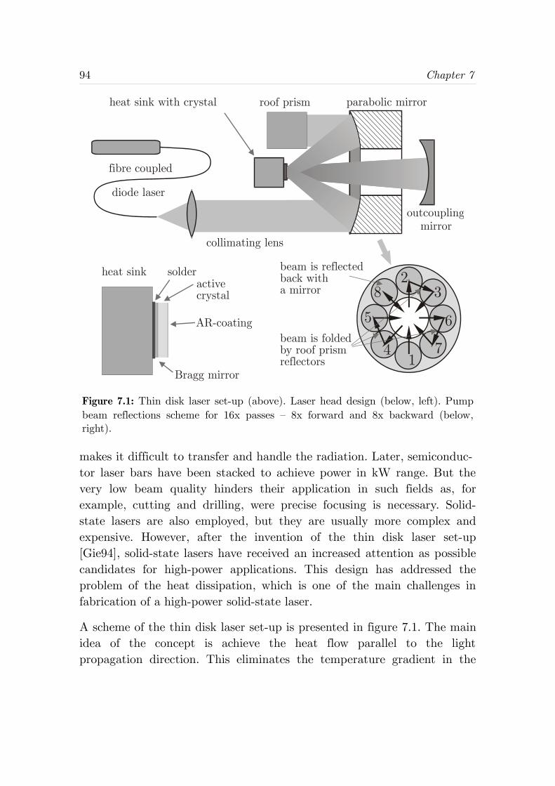
94 Chapter 7
makes it difficult to transfer and handle the radiation. Later, semiconduc-tor laser bars have been stacked to achieve power in kW range. But thevery low beam quality hinders their application in such fields as, forexample, cutting and drilling, were precise focusing is necessary. Solid-state lasers are also employed, but they are usually more complex andexpensive. However, after the invention of the thin disk laser set-up[Gie94], solid-state lasers have received an increased attention as possiblecandidates for high-power applications. This design has addressed theproblem of the heat dissipation, which is one of the main challenges infabrication of a high-power solid-state laser.
A scheme of the thin disk laser set-up is presented in figure 7.1. The mainidea of the concept is achieve the heat flow parallel to the lightpropagation direction. This eliminates the temperature gradient in the
1
23
4
5 6
7
8
fibre coupled
collimating lens
roof prism parabolic mirrorheat sink with crystal
outcouplingmirror
heat sink solder
Bragg mirror
AR-coating
diode laser
beam is foldedby roof prismreflectors
active crystal
beam is reflectedback with a mirror
Figure 7.1: Thin disk laser set-up (above). Laser head design (below, left). Pumpbeam reflections scheme for 16x passes – 8x forward and 8x backward (below,right).
Ytterbium-Doped PLD-Films 95
lateral direction, accordingly eliminating the thermal lens effect, whichoften limits the achievable output of a solid-state laser.
Additionally, thin active crystals (disks) and large laser mode diametersare utilized, thus even further improving the heat flow and the reducingthermal load. Nowadays, disks with the thickness down to 100 μm areused. However, this raises the problem of low absorption of the pumplight in the thin active medium. The typically used solution is to fold thepump beam and make it pass the crystal several times (as presented infigure 7.1). Sometimes also side pumping is employed. In this case thelight of the laser diode is focused into the active crystal, so that it isguided inside of the crystal due to the total internal reflection.
Why Pulsed Laser Deposition?
The typical way of fabrication of active media for a thin disk laser is tocut a disk out of a grown bulk crystal and polish it to the necessarythickness and quality. Sometimes it is subsequently bonded onto anundoped substrate for mechanical stability. On the one side the high-reflective dielectric Bragg mirror (HR) for both pump and laserwavelengths is deposited, the other side is usually anti-reflex (AR) coated.Afterwards the mirrored side of the crystal is soldered onto a heat sink.
However, some difficulties may arise during fabrication and handling ofsuch thin crystals (a few 100 μm), as well as during bonding them onto aheat sink. An alternative technique is a deposition of the active materialdirectly onto an undoped substrate. Following this route, Ubizskii et al.produced highly Yb-doped epitaxial YAG films by liquid-phase epitaxy(LPE), which subsequently showed continuous-wave laser action in a thindisk set-up [Ubi04]. However, unidentified absorption bands and lifetimereduction have been observed in some films, possibly due tocontamination from the flux. The pulsed laser deposition can be an evenmore favorable technique. In principle, it allows fabrication of high qualitycrystalline films with high peak emission and absorption cross-sections ofdopants. Another important quality of PLD is that, due to the nature ofthe process, it minimizes the possibility of contamination of the depositedfilms. In the contrast to LPE, where impurities can be incorporated from
96 Chapter 7
the flux, or to classical crystal growth methods, where impurities arepresent in the crucible material, in the PLD process the material istransferred directly from a target onto a substrate in vacuum or suitableatmosphere. The only limiting factor in this case is the purity of thesource materials. As it will be discussed below impurities are animportant issue for highly Yb-doped materials.
Alternating the materials used for evaporation, also the dielectric coatings(Bragg mirror and anti-reflection coating) could be fabricated by pulsedlaser deposition. Pulsed-laser-deposited films typically reveal thecrystalline character with the density approaching that of a bulk crystal.This ensures high refractive index and mechanical stability of the films.The fact, that the active media for thin disk laser together with allcoatings can be produced in one technological process, makes pulsed laserdeposition a very interesting technique for this application. Up to now, noresearch in this area have been noticed. All investigations of activePLD-films were carried out with respect to their possible applications asactive media for waveguide lasers or amplifiers. The PLD-films reportedin the literature typically have the thickness of a few micrometers, whichis not enough for thin disk laser applications. However, in the course ofthese work a Nd:Sc2O3 waveguiding PLD-film with the thickness of 10 μmhave been successfully fabricated (see section 6.3). Also some examples ofthick PLD-films can be found in the literature: up to 12 μm Ti:Sapphire[And97a, And97b], up to 135 μm Nd:GGG [Gri04b]. Thus, the filmthicknesses, that are necessary for a thin disk laser, seems to beachievable with the pulsed laser deposition.
7.1.2 Microcavities
Another possible application for pulsed-laser-deposited, layered structurescould be fabrication of compact devices such as, for example, Fabri-Perotmicrocavities. A microcavity consists of two Bragg mirrors (interchanginghigh and low refractive index layers with the optical thickness of a quarterdesign wavelength) and a cavity with optical thickness multiple to a halfof the design wavelength. Otherwise a microcavity can be considered aone-dimensional photonic crystal (periodic structure) with a defect
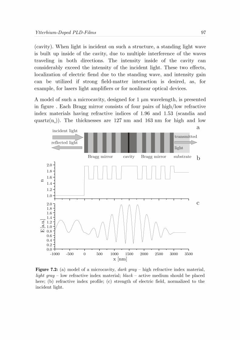
Ytterbium-Doped PLD-Films 97
(cavity). When light is incident on such a structure, a standing light waveis built up inside of the cavity, due to multiple interference of the wavestraveling in both directions. The intensity inside of the cavity canconsiderably exceed the intensity of the incident light. These two effects,localization of electric fiend due to the standing wave, and intensity gaincan be utilized if strong field-matter interaction is desired, as, forexample, for lasers light amplifiers or for nonlinear optical devices.
A model of such a microcavity, designed for 1 μm wavelength, is presentedin figure . Each Bragg mirror consists of four pairs of high/low refractiveindex materials having refractive indices of 1.96 and 1.53 (scandia andquartz(no)). The thicknesses are 127 nm and 163 nm for high and low
Figure 7.2: (a) model of a microcavity, dark gray – high refractive index material,light gray – low refractive index material; black – active medium should be placedhere; (b) refractive index profile; (c) strength of electric field, normalized to theincident light.
incident light
reflected lighttransmitted
light
Bragg mirror Bragg mirrorcavity
a
b
c
substrate
-1000 -500 0 500 1000 1500 2000 2500 3000 35000.00.20.40.60.81.01.21.41.61.82.0
E[a
.u.]
x [nm]
1.01.21.41.61.82.0
n
98 Chapter 7
index layers, respectively. Scandia has also been taken as the cavitymaterial. The thickness of the cavity is 508 nm, thus the optical lengthcorresponds to one design wavelength. The distribution of the amplitudeof the electric field E (figure c) has been calculated using the transfer-matrix method (TMM). It is normalized to the amplitude of the incidentlight. The varying amplitude in the region to the left of the structure iscaused by the interference with the reflected light. For the presented case,the field strength in the cavity is about two times higher than that of theincident light. For the intensity the effect is larger, since it is proportionalto the square of the electrical field. In order to achieve stronger effect, thereflectivity of the mirrors should be improved. Either more pairs ofhigh/low index layers or materials with higher refractive index contrastshould be used. In the discussed case reflectivity of both Bragg mirrors isonly about 70% at the design wavelength.
The first theoretical investigations of microcavity effect was done byPurcell [Pur46]. But the first microchip laser was demonstrated muchlater by De Martini [DeM88]. Details on microcavity effects andmicrocavity lasers can be found for example in a review by G. Björk[Bjö96]. In recent time also enhancement of nonlinear light-matterinteraction in microcavities received much attention, e.g. Bosco et al.[Bos04] have experimentally demonstrated second harmonic generation(SHG) in a one-dimensional AlGaAs/Al2O3 photonic structure. Themicrocavity effect is also utilized in vertical cavity semiconductor lasers[Tro04].
However, further research is still required in order to achieve the accuracyin the control of the pulsed laser deposition process, which is necessary todeposit such complex structures.
7.1.3 Ytterbium-Doped Materials
Originally, Nd-doped materials have been widely used as an activemedium for high-power lasers. The Nd3+-ion has high absorption andemission cross-sections in many materials and laser operation with itsfour-level scheme for the 4F3/2→
4I11/2 transition is easy to realize. Also
Ytterbium-Doped PLD-Films 99
suitable high-power laser diodes as pump source are commerciallyavailable. All this make Nd-doped materials a favorable choice.
However, the invention of the thin disk laser set-up stimulated anincreasing interest to the Yb-doped oxide materials. Due to a smallerquantum defect compared to the widely used Nd-doped materials, theheat dissipation is reduced, thus even further minimizing thermallyinduced problems. The very simple energy level structure of the Yb3+-ionalso eliminates the possibility of the depopulation of the upper laser leveldue to cross-relaxation and up-conversion processes and nonradiativedecay. This is an important advantage at high doping concentrations andpump rates used in a thin disk laser. Due to relatively broad emissionlines, Yb-doped materials are also suitable for mode-locked operationregimes.
The most widely used host material for Yb3+-ions is yttrium aluminumgarnet (YAG), which is also a classical host material for the Nd3+-dopant.This is due to favorable spectroscopic properties of Yb:YAG, developedgrowth technology of YAG crystals, and low cost of source materials. It ismechanically stable and reveals high thermal conductivity. For example, aYb:YAG thin disk laser with output power of 650 W using one disk or1070 W using four disks has been demonstrated [Ste00]. Also a mode-locked Yb:YAG thin disk laser has been used recently to demonstrate amulti-watt RGB laser source [Bru04].
Apart from YAG, the sesquioxides (e.g. Sc2O3, Y2O3, Lu2O3) are verypromising host materials for high-power laser applications [Pet02b]. Theirthermal conductivity is even higher than that of YAG (see table 2.1). Alsovery high absorption and emission cross-sections of trivalent rare-earthions in these materials make them an interesting alternative. Effectivemode-locked laser operation has been also demonstrated recently usingYb:Sc2O3 [Klo04] and Yb:Lu2O3 [Grib04] single crystals. Details on thespectroscopic and lasing properties of Yb-doped sesquioxides can be foundin [Mix99] and [Pet01].
Lutetia is possibly the most interesting among the sesquioxides as a hostmaterial for Yb3+-ions. Lu3+ and Yb3+ ions in the sixfold coordination have
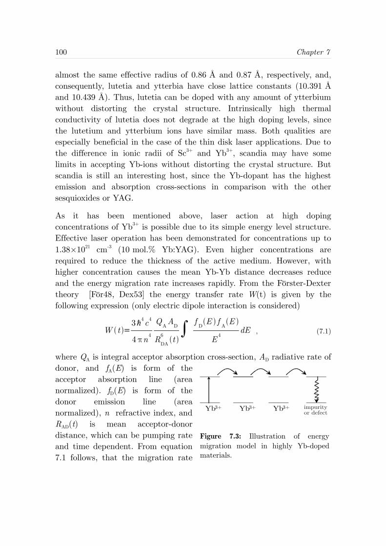
100 Chapter 7
almost the same effective radius of 0.86 Å and 0.87 Å, respectively, and,consequently, lutetia and ytterbia have close lattice constants (10.391 Åand 10.439 Å). Thus, lutetia can be doped with any amount of ytterbiumwithout distorting the crystal structure. Intrinsically high thermalconductivity of lutetia does not degrade at the high doping levels, sincethe lutetium and ytterbium ions have similar mass. Both qualities areespecially beneficial in the case of the thin disk laser applications. Due tothe difference in ionic radii of Sc3+ and Yb3+, scandia may have somelimits in accepting Yb-ions without distorting the crystal structure. Butscandia is still an interesting host, since the Yb-dopant has the highestemission and absorption cross-sections in comparison with the othersesquioxides or YAG.
As it has been mentioned above, laser action at high dopingconcentrations of Yb3+ is possible due to its simple energy level structure.Effective laser operation has been demonstrated for concentrations up to1.38×1021 cm-3 (10 mol.% Yb:YAG). Even higher concentrations arerequired to reduce the thickness of the active medium. However, withhigher concentration causes the mean Yb-Yb distance decreases reduceand the energy migration rate increases rapidly. From the Förster-Dextertheory [För48, Dex53] the energy transfer rate W(t) is given by thefollowing expression (only electric dipole interaction is considered)
W t =3ℏ4c4
4πn4
QAA
D
RDA
6t ∫ f
DE f
AE
E 4dE , (7.1)
where QA is integral acceptor absorption cross-section, AD radiative rate ofdonor, and fA(E) is form of theacceptor absorption line (areanormalized). fD(E) is form of thedonor emission line (areanormalized), n refractive index, andRAD(t) is mean acceptor-donordistance, which can be pumping rateand time dependent. From equation7.1 follows, that the migration rate
Figure 7.3: Illustration of energymigration model in highly Yb-dopedmaterials.
Yb3+ Yb3+ Yb3+ impurity or defect
Ytterbium-Doped PLD-Films 101
increases inversely proportional to the sixth power of the interionicdistance. Fast migration rates lead to the situation, when the excitation israpidly transferred from ion to ion and can be finally transferred to animpurity or a defect (see figure 7.3), which can be radiatively ornonradiatively deexcited. It has been shown that impurities in the ppmrange can cause significant quantum efficiency degradation at high Yb-concentrations [Pet05]. Degradation of the efficiency at high pumpingrates in Yb:YAG crystals have been reported as well [Lar05].
§7.2 Characterization of Yb-Doped PLD-films
7.2.1 Ytterbia Films
Since the thickness of the active medium in the thin disk laser set-up is aconcern, ytterbia (Yb2O3) can be a possible candidate. Due to the veryhigh Yb3+ density, it would result in the thinest possible design for a givenabsorption among all Yb-doped materials.
Two series of ytterbia films with different thicknesses in the range of20 nm – 500 nm were deposited on sapphire and quartz substrates1. TheX-ray diffraction analysis of the films were performed in order toinvestigate the crystalline structure of the films. These results as well asthe fabrication conditions are discussed in detail in section 5.1. The filmsdeposited both on sapphire and on quartz substrates are crystalline andhighly textured in <111>-direction. Room temperature spectroscopicmeasurements were performed under continuous IR excitation using aTi:Sapphire laser and under pulsed IR excitation with an OPO. In bothcases no Yb3+-emission could be detected. Emission measurements of theytterbia films under UV excitation have been performed at theSuperLumi experimental set-up. The mentioned experimental set-ups aredescribed in section 3.4.
Figure 7.4 shows the emission spectra of the 500 nm thick Yb2O3 film on aquartz substrate under 220 nm excitation. The spectra reveal the well-known Yb3+ (4F5/2→
4F7/2) emission in the 975 nm – 990 nm spectral region
1 Y01, Y02, Y04 and Y07-Y09 (appendix A).
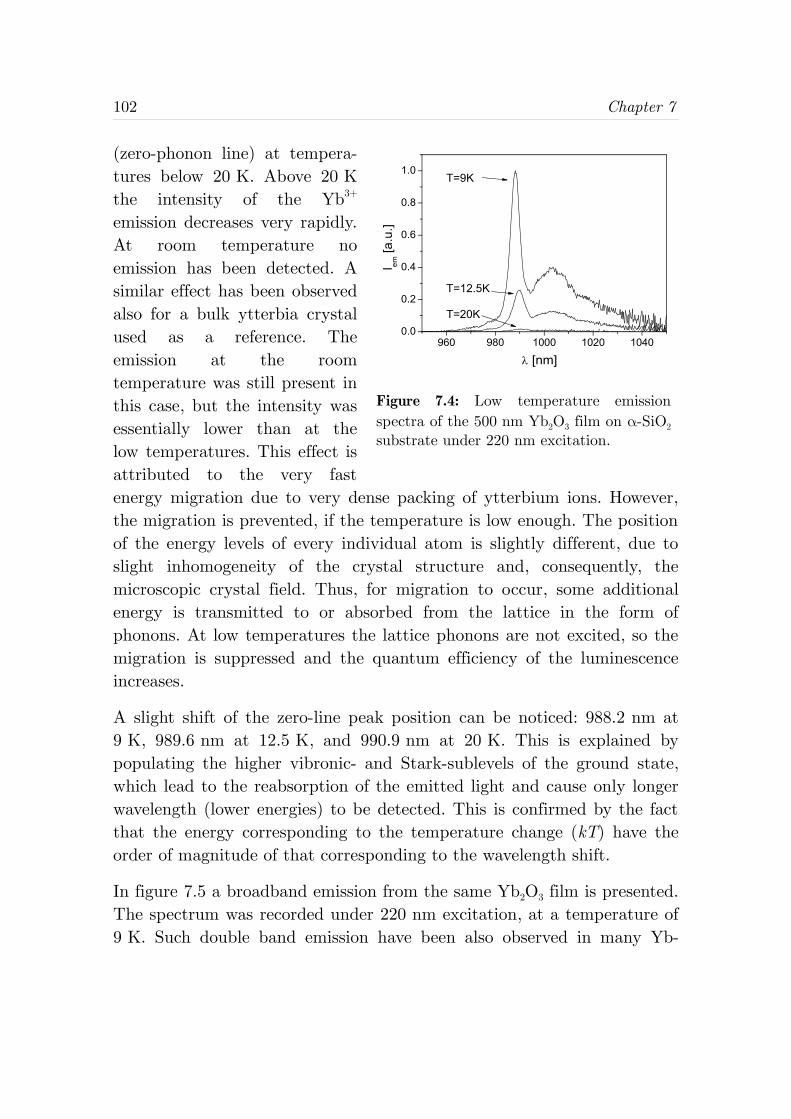
102 Chapter 7
(zero-phonon line) at tempera-tures below 20 K. Above 20 Kthe intensity of the Yb3+
emission decreases very rapidly.At room temperature noemission has been detected. Asimilar effect has been observedalso for a bulk ytterbia crystalused as a reference. Theemission at the roomtemperature was still present inthis case, but the intensity wasessentially lower than at thelow temperatures. This effect isattributed to the very fastenergy migration due to very dense packing of ytterbium ions. However,the migration is prevented, if the temperature is low enough. The positionof the energy levels of every individual atom is slightly different, due toslight inhomogeneity of the crystal structure and, consequently, themicroscopic crystal field. Thus, for migration to occur, some additionalenergy is transmitted to or absorbed from the lattice in the form ofphonons. At low temperatures the lattice phonons are not excited, so themigration is suppressed and the quantum efficiency of the luminescenceincreases.
A slight shift of the zero-line peak position can be noticed: 988.2 nm at9 K, 989.6 nm at 12.5 K, and 990.9 nm at 20 K. This is explained bypopulating the higher vibronic- and Stark-sublevels of the ground state,which lead to the reabsorption of the emitted light and cause only longerwavelength (lower energies) to be detected. This is confirmed by the factthat the energy corresponding to the temperature change (kT) have theorder of magnitude of that corresponding to the wavelength shift.
In figure 7.5 a broadband emission from the same Yb2O3 film is presented.The spectrum was recorded under 220 nm excitation, at a temperature of9 K. Such double band emission have been also observed in many Yb-
Figure 7.4: Low temperature emissionspectra of the 500 nm Yb2O3 film on α-SiO2
substrate under 220 nm excitation.
960 980 1000 1020 10400.0
0.2
0.4
0.6
0.8
1.0
T=20K
T=12.5K
I em [a
.u.]
λ [nm]
T=9K
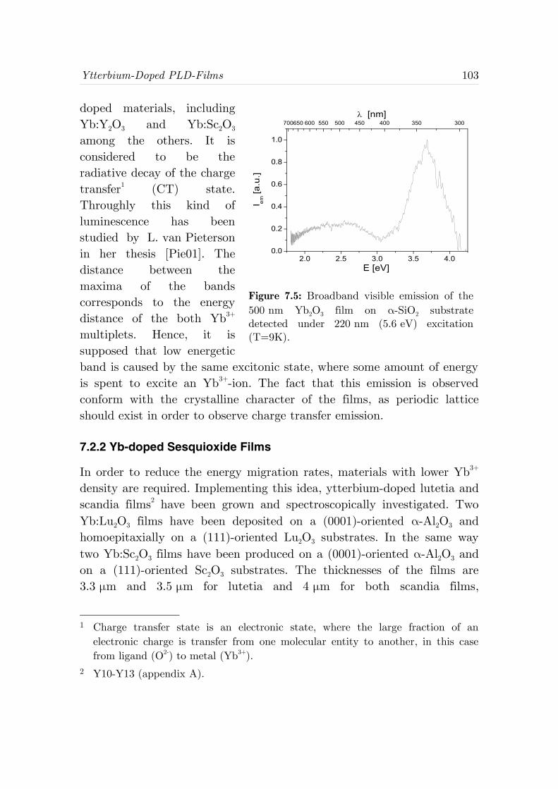
Ytterbium-Doped PLD-Films 103
doped materials, includingYb:Y2O3 and Yb:Sc2O3
among the others. It isconsidered to be theradiative decay of the chargetransfer1 (CT) state.Throughly this kind ofluminescence has beenstudied by L. van Pietersonin her thesis [Pie01]. Thedistance between themaxima of the bandscorresponds to the energydistance of the both Yb3+
multiplets. Hence, it issupposed that low energeticband is caused by the same excitonic state, where some amount of energyis spent to excite an Yb3+-ion. The fact that this emission is observedconform with the crystalline character of the films, as periodic latticeshould exist in order to observe charge transfer emission.
7.2.2 Yb-doped Sesquioxide Films
In order to reduce the energy migration rates, materials with lower Yb3+
density are required. Implementing this idea, ytterbium-doped lutetia andscandia films2 have been grown and spectroscopically investigated. TwoYb:Lu2O3 films have been deposited on a (0001)-oriented α-Al2O3 andhomoepitaxially on a (111)-oriented Lu2O3 substrates. In the same waytwo Yb:Sc2O3 films have been produced on a (0001)-oriented α-Al2O3 andon a (111)-oriented Sc2O3 substrates. The thicknesses of the films are3.3 μm and 3.5 μm for lutetia and 4 μm for both scandia films,
1 Charge transfer state is an electronic state, where the large fraction of anelectronic charge is transfer from one molecular entity to another, in this casefrom ligand (O2-) to metal (Yb3+).
2 Y10-Y13 (appendix A).
Figure 7.5: Broadband visible emission of the500 nm Yb2O3 film on α-SiO2 substratedetected under 220 nm (5.6 eV) excitation(T=9K).
2.0 2.5 3.0 3.5 4.00.0
0.2
0.4
0.6
0.8
1.0
700650 600 550 500 450 400 350 300λ [nm]
I em [a
.u.]
E [eV]
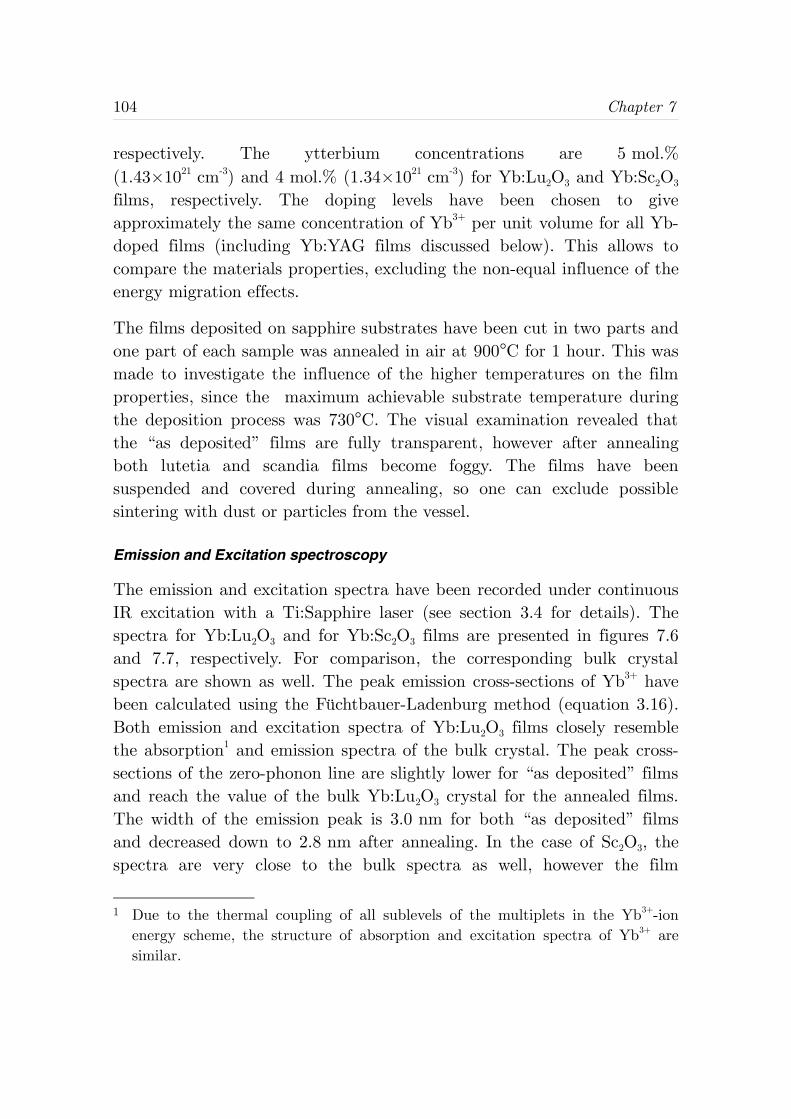
104 Chapter 7
respectively. The ytterbium concentrations are 5 mol.%(1.43×1021 cm-3) and 4 mol.% (1.34×1021 cm-3) for Yb:Lu2O3 and Yb:Sc2O3
films, respectively. The doping levels have been chosen to giveapproximately the same concentration of Yb3+ per unit volume for all Yb-doped films (including Yb:YAG films discussed below). This allows tocompare the materials properties, excluding the non-equal influence of theenergy migration effects.
The films deposited on sapphire substrates have been cut in two parts andone part of each sample was annealed in air at 900°C for 1 hour. This wasmade to investigate the influence of the higher temperatures on the filmproperties, since the maximum achievable substrate temperature duringthe deposition process was 730°C. The visual examination revealed thatthe “as deposited” films are fully transparent, however after annealingboth lutetia and scandia films become foggy. The films have beensuspended and covered during annealing, so one can exclude possiblesintering with dust or particles from the vessel.
Emission and Excitation spectroscopy
The emission and excitation spectra have been recorded under continuousIR excitation with a Ti:Sapphire laser (see section 3.4 for details). Thespectra for Yb:Lu2O3 and for Yb:Sc2O3 films are presented in figures 7.6and 7.7, respectively. For comparison, the corresponding bulk crystalspectra are shown as well. The peak emission cross-sections of Yb3+ havebeen calculated using the Füchtbauer-Ladenburg method (equation 3.16).Both emission and excitation spectra of Yb:Lu2O3 films closely resemblethe absorption1 and emission spectra of the bulk crystal. The peak cross-sections of the zero-phonon line are slightly lower for “as deposited” filmsand reach the value of the bulk Yb:Lu2O3 crystal for the annealed films.The width of the emission peak is 3.0 nm for both “as deposited” filmsand decreased down to 2.8 nm after annealing. In the case of Sc2O3, thespectra are very close to the bulk spectra as well, however the film
1 Due to the thermal coupling of all sublevels of the multiplets in the Yb3+-ionenergy scheme, the structure of absorption and excitation spectra of Yb3+ aresimilar.
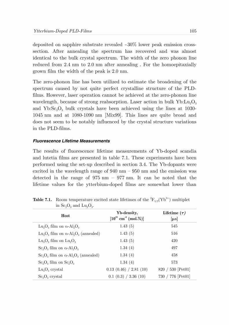
Ytterbium-Doped PLD-Films 105
deposited on sapphire substrate revealed ~30% lower peak emission cross-section. After annealing the spectrum has recovered and was almostidentical to the bulk crystal spectrum. The width of the zero phonon linereduced from 2.4 nm to 2.0 nm after annealing . For the homoepitaxiallygrown film the width of the peak is 2.0 nm.
The zero-phonon line has been utilized to estimate the broadening of thespectrum caused by not quite perfect crystalline structure of the PLD-films. However, laser operation cannot be achieved at the zero-phonon linewavelength, because of strong reabsorption. Laser action in bulk Yb:Lu2O3
and Yb:Sc2O3 bulk crystals have been achieved using the lines at 1030-1045 nm and at 1080-1090 nm [Mix99]. This lines are quite broad anddoes not seem to be notably influenced by the crystal structure variationsin the PLD-films.
Fluorescence Lifetime Measurements
The results of fluorescence lifetime measurements of Yb-doped scandiaand lutetia films are presented in table 7.1. These experiments have beenperformed using the set-up described in section 3.4. The Yb-dopants wereexcited in the wavelength range of 940 nm – 950 nm and the emission wasdetected in the range of 975 nm – 977 nm. It can be noted that thelifetime values for the ytterbium-doped films are somewhat lower than
Table 7.1. Room temperature excited state lifetimes of the 2F5/2(Yb3+) multiplet in Sc2O3 and Lu2O3.
HostYb-density,
[1021 cm-3 (mol.%)]Lifetime (τ)
[μs]
Lu2O3 film on α-Al2O3 1.43 (5) 545
Lu2O3 film on α-Al2O3 (annealed) 1.43 (5) 516
Lu2O3 film on Lu2O3 1.43 (5) 420
Sc2O3 film on α-Al2O3 1.34 (4) 497
Sc2O3 film on α-Al2O3 (annealed) 1.34 (4) 458
Sc2O3 film on Sc2O3 1.34 (4) 573
Lu2O3 crystal 0.13 (0.46) / 2.81 (10) 820 / 530 [Pet01]
Sc2O3 crystal 0.1 (0.3) / 3.36 (10) 730 / 776 [Pet01]
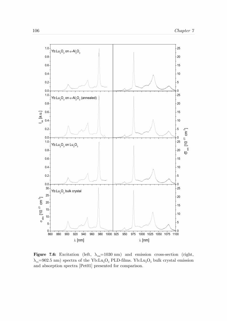
106 Chapter 7
Figure 7.6: Excitation (left, λem=1030 nm) and emission cross-section (right,λex=902.5 nm) spectra of the Yb:Lu2O3 PLD-films. Yb:Lu2O3 bulk crystal emissionand absorption spectra [Pet01] presented for comparison.
0.0
0.2
0.4
0.6
0.8
1.0
0
5
10
15
20
25
Yb:Lu2O3 bulk crystal
Yb:Lu2O3 on Lu2O3
Yb:Lu2O3 on α-Al2O3 (annealed)
Yb:Lu2O3 on α-Al2O3
0.0
0.2
0.4
0.6
0.8
1.0
σab
s [10
-21 c
m2 ]
I ex [a
.u.]
0
5
10
15
20
25
σem
[10
-21 c
m2 ]
0.0
0.2
0.4
0.6
0.8
1.0
0
5
10
15
20
25
860 880 900 920 940 960 980 10000
5
10
15
20
25
30
λ [nm]925 950 975 1000 1025 1050 1075 1100
0
5
10
15
20
25
λ [nm]
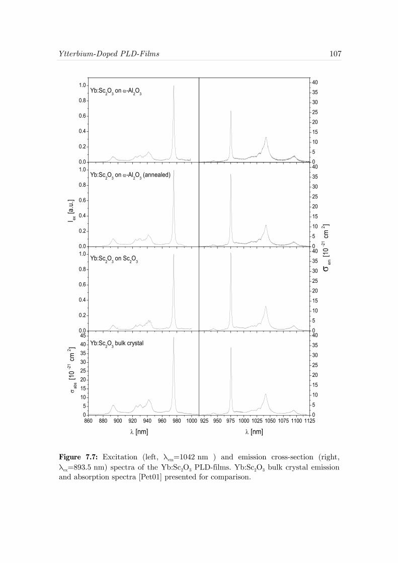
Ytterbium-Doped PLD-Films 107
Figure 7.7: Excitation (left, λem=1042 nm ) and emission cross-section (right,λex=893.5 nm) spectra of the Yb:Sc2O3 PLD-films. Yb:Sc2O3 bulk crystal emissionand absorption spectra [Pet01] presented for comparison.
0.0
0.2
0.4
0.6
0.8
1.0
0
5
10
15
20
25
30
35
40
Yb:Sc2O3 bulk crystal
Yb:Sc2O3 on Sc2O3
Yb:Sc2O3 on α-Al2O3 (annealed)
Yb:Sc2O3 on α-Al2O3
0.0
0.2
0.4
0.6
0.8
1.0
I ex [a
.u.]
0
5
10
15
20
25
30
35
40
σem
[10
-21 c
m2 ]
0.0
0.2
0.4
0.6
0.8
1.0
0
5
10
15
20
25
30
35
40
860 880 900 920 940 960 980 100005
1015202530354045
σab
s [10
-21 c
m2 ]
λ [nm]925 950 975 1000 1025 1050 1075 1100 1125
0
5
10
15
20
25
30
35
40
λ [nm]
108 Chapter 7
that of the corresponding bulk crystal. This indicates that quantumefficiency of the Yb3+ luminescence is reduced, presumably due to higherdensity of crystal lattice defects. The quantum efficiency can be estimatedusing equation 3.18 and was found to be in the range of 51%-66% for theYb:Lu2O3 films and 68%-78% for Yb:Sc2O3 films. The fluorescence decaylifetimes for the low-doped bulk crystals have been taken as the radiativelifetimes. This assumption can be made, since at such low concentrationsthe migration rate to the defects or impurities is negligible and otherdeexcitation channels are not present in the Yb3+-ion. These lifetimesvalues have been also used in equation 3.16 for calculations of emissioncross-sections.
The lifetime drop for the annealed lutetia and scandia films in thecomparison with the “as deposited” films should be mentioned. Howeverup to now no explanation for this effect have been found. Since improvedcrystallinity, as it follows from the sharper spectral lines, and higher peakcross-sections, should also result in lower defect density and longerlifetimes. One of the possible explanations can be increased migrationrate, due to the reduced inhomogeneous broadening and better overlap ofthe energy levels of individual Yb3+-ions.
7.2.3 Yb-doped YAG Films
Currently, Yb-doped yttrium-aluminum garnet is the most widely usedhost material for thin disk lasers. This section presents the results ofspectroscopic investigations of Yb-doped YAG PLD films.
Two Yb:YAG have been deposited on a (0001)-oriented α-Al2O3 substrateand homoepitaxially on a (100)-oriented YAG substrate1. Subsequentlyboth samples have been cut in two parts and one half of each sample hasbeen annealed in the air at 1100°C during 1 hour. Again, as in the case ofsesquioxide films, the annealed samples have been found to be foggy.Crystalline structure investigation and deposition parameters of the YAGfilms are discussed in section 5.2. Briefly, the XRD analysis showed that
1 Y14-Y15 (appendix A).

Ytterbium-Doped PLD-Films 109
the “as deposited” films are amorphous and the annealed samples showedpolycrystalline behavior.
Emission and Excitation spectroscopy
Both excitation and emission spectra of “as deposited” films do not showthe typical Yb:YAG spectra (figure 7.8). The zero-phonon line can beeasily identified, however it is broadened and the broad band emission isobserved instead of the expected side bands. The position of the zerophonon line and the intensity distribution has been found to resemble theabsorption1 and emission spectra of Yb:Y2O3 more closely than those ofYb:YAG. The annealed films on the contrary reveal the well-known,almost undistorted Yb:YAG spectra. Thus it can be concluded that thedeposition temperature of 700°C was not high enough for the YAG latticeto build up and the deposited films are amorphous or, possibly,nanocrystallites of Yb:Y2O3 are formed. It seems, that temperatureshigher than 700°C is required for YAG lattice to beformed. The resultsconfirming this fact are observed, when amorphous 100 nm Eu:Y2O3 filmson sapphire substrates have been annealed at the different temperatures[Bär05]. Up 1000°C typical Eu:Y2O3 spectrum was observed, but for thetemperatures over 1000°C also Eu:YAG lines appear in the spectrum. Inthis case YAG was formed due to mutual indiffusion of Y2O3 and Al2O3.Similar effect have been observed by C. Grivas et al. for Nd-dopedgadolinium-gallium garnet (GGG) films deposited at 650°C. The emissionspectra of Nd3+ was noticeably broadened [Gri04a], in spite of the factthat the x-ray diffraction analysis have shown epitaxial growth of theNd:GGG films on YAG substrates [Gri04b].
Fluorescence Lifetime Measurements
The result of the fluorescence lifetime measurements of the 2F5/2 multipletof Yb3+-ion in the Yb:YAG films are presented in table 7.2. Yb3+-ions wereexcited at the wavelength of 940-950 nm and emission at 975 nm or
1 Due to the thermal coupling of all sublevels of the multiplets in the Yb3+-ionenergy scheme, the structure of absorption and excitation spectra of Yb3+ aresimilar.
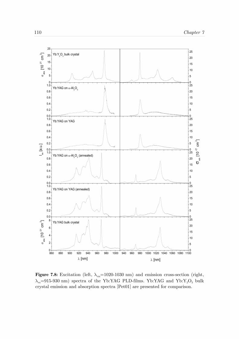
110 Chapter 7
Figure 7.8: Excitation (left, λem=1020-1030 nm) and emission cross-section (right,λex=915-930 nm) spectra of the Yb:YAG PLD-films. Yb:YAG and Yb:Y2O3 bulkcrystal emission and absorption spectra [Pet01] are presented for comparison.
0
5
10
15
20
25
σab
s [10
-21 c
m2 ]
σab
s [10
-21 c
m2 ]
0
5
10
15
20
25
Yb:YAG on YAG (annealed)
Yb:YAG on α-Al2O
3 (annealed)
Yb:YAG bulk crystal
Yb:YAG on YAG
Yb:YAG on α-Al2O
3
Yb:Y2O
3 bulk crystal
0.0
0.2
0.4
0.6
0.8
1.0
I ex [a
.u.]
0
5
10
15
20
25
σem
[10
-21 c
m2 ]
0.0
0.2
0.4
0.6
0.8
1.0
0
5
10
15
20
25
0.0
0.2
0.4
0.6
0.8
1.0
0
5
10
15
20
25
0.0
0.2
0.4
0.6
0.8
1.0
0
5
10
15
20
25
860 880 900 920 940 960 980 10000
2
4
6
8
940 960 980 1000 1020 1040 1060 1080 11000
5
10
15
20
25
λ [nm] λ [nm]
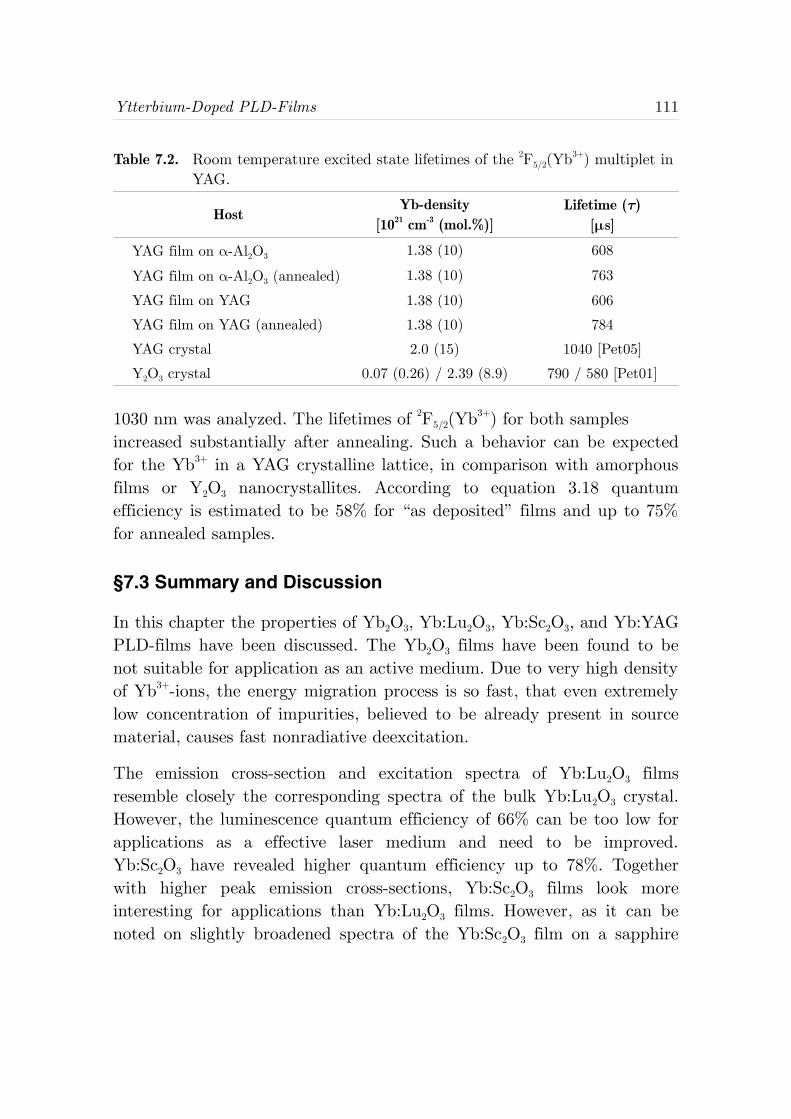
Ytterbium-Doped PLD-Films 111
1030 nm was analyzed. The lifetimes of 2F5/2(Yb3+) for both samplesincreased substantially after annealing. Such a behavior can be expectedfor the Yb3+ in a YAG crystalline lattice, in comparison with amorphousfilms or Y2O3 nanocrystallites. According to equation 3.18 quantumefficiency is estimated to be 58% for “as deposited” films and up to 75%for annealed samples.
§7.3 Summary and Discussion
In this chapter the properties of Yb2O3, Yb:Lu2O3, Yb:Sc2O3, and Yb:YAGPLD-films have been discussed. The Yb2O3 films have been found to benot suitable for application as an active medium. Due to very high densityof Yb3+-ions, the energy migration process is so fast, that even extremelylow concentration of impurities, believed to be already present in sourcematerial, causes fast nonradiative deexcitation.
The emission cross-section and excitation spectra of Yb:Lu2O3 filmsresemble closely the corresponding spectra of the bulk Yb:Lu2O3 crystal.However, the luminescence quantum efficiency of 66% can be too low forapplications as a effective laser medium and need to be improved.Yb:Sc2O3 have revealed higher quantum efficiency up to 78%. Togetherwith higher peak emission cross-sections, Yb:Sc2O3 films look moreinteresting for applications than Yb:Lu2O3 films. However, as it can benoted on slightly broadened spectra of the Yb:Sc2O3 film on a sapphire
Table 7.2. Room temperature excited state lifetimes of the 2F5/2(Yb3+) multiplet inYAG.
HostYb-density
[1021 cm-3 (mol.%)]Lifetime (τ)
[μs]
YAG film on α-Al2O3 1.38 (10) 608
YAG film on α-Al2O3 (annealed) 1.38 (10) 763
YAG film on YAG 1.38 (10) 606
YAG film on YAG (annealed) 1.38 (10) 784
YAG crystal 2.0 (15) 1040 [Pet05]
Y2O3 crystal 0.07 (0.26) / 2.39 (8.9) 790 / 580 [Pet01]
112 Chapter 7
substrate, deposition parameters still need some optimization. Though,since the annealing at the temperature of 900°C eliminated thisbroadening effect, it does not seem to be a fundamental problem.
The “as deposited” Yb:YAG films revealed very poor spectroscopicproperties. The films deposited at 700°C did not reveal spectracharacteristic for Yb:YAG. After annealing at 1200°C typical Yb:YAGspectra and improved lifetimes have been observed. The quantumefficiency of the luminescence was found to be up to 75% for the annealedfilms. It can be concluded that the higher substrate temperatures arerequired for the deposition of the crystalline Yb:YAG films directly.
The effect of the annealing is found to be quite contradictory. On the oneside it eliminates the spectral broadening. On the other side, in the caseof the Yb-doped sesquioxide films, it caused degraded lifetimes of theexcited state of Yb3+. The fact, that all annealed films become partlyscattering (foggy), is another drawback of the annealing. Presumablyrecrystallization at the surface can be a reason for this effect. Quitesimilar destruction of the surface structure was observed after annealingof bulk sesquioxides crystals.
The influence of the substrate on the spectroscopic properties of the filmhas been noticed for the case of Yb:Sc2O3 film. The spectra of the filmdeposited on the sapphire substrate was slightly broadened. This effectcannot be explained by poorer crystallinity of the film in comparison withthe homoepitaxially grown film, since the XRD analysis shows crystallinesin the range of hundreds of nanometers. In the case of Lu2O3 the substratehave not influenced the spectroscopic properties of the deposited films.Spectra of the homoepitaxially deposited Yb:Lu2O3 film have been slightlybroadened, as well as the spectra of the film deposited on a sapphiresubstrate.
Chapter 8. Conclusions
The subject of this thesis was the characterization of rare-earth-dopedoxide films fabricated by pulsed laser deposition and the analysis of theirpossible application as active media, e.g for waveguide or thin disk lasers.The experimental results of the film preparation, the XRD analysis, thecharacterization of the waveguiding films, and the properties of the Yb-doped films were summarized at the end of chapters 4-7, respectively.This chapter resumes the results of this thesis and gives an outlook forfuture research.
§8.1 Summary of Results
Crystalline sesquioxide (scandia, yttria, ytterbia, and lutetia) PLD-filmshave been successfully grown in the course of this work. In case of scandiathe properties of the films depending on the deposition parameters havebeen investigated in more detail.
As follows from the XRD investigations of the sesquioxide films in theframework of this thesis as well as from the results of previous works inthe solid-state laser group at University of Hamburg [Bur02, Bär04,Rab04], higher crystalline quality is achieved for scandia PLD-filmscompared to lutetia or yttria films deposited under similar conditions.This effect is due to the low mass of the scandium ion and, consequently,the high mobility on the substrate surface, which results in a moreeffective lattice formation. For the 500 nm Sc2O3 films on sapphiresubstrates a lower limit for the crystallite dimensions was estimated to beabout 330 nm. The real dimensions cannot be determined, since theresolution limit of the diffractometer was reached. In case of lutetia acomparable crystalline quality is achieved only for homoepitaxially grownPLD-films. The films deposited on sapphire substrates reveal crystallites
114 Chapter 8
sizes in the range of several tens of nanometers. The ytterbia films onsapphire substrates behave similarly.
The spectroscopic investigations on the Yb-doped scandia and lutetiafilms reveal, that their emission and excitation spectra resemble closelythose of bulk crystals. Lower crystalline quality of lutetia films comparedto scandia ones causes stronger broadening of the Yb-dopant emission andexcitation spectra. In case of the Nd-doped scandia films the spectra areslightly broadened and the peak cross-sections reach about 70% of thoseof the bulk crystal values. The Eu-doped yttria film show bulk-likespectra.
Both for the Nd- and the Yb-doped films a decrease in the lifetime of theexcited states compared to the corresponding bulk crystal is observed.This effect is due to the higher lattice defect density and the localsymmetry distortion in the film structure compared to the bulk crystal.However, these negative effects are not dramatic and the spectroscopicproperties of the Yb-doped films can be considered promising forapplications as active media.
The ytterbia films show very poor spectroscopic properties, whichpresumably results from impurities present in the source material. TheYb:YAG PLD-films grown under conditions similar to that used for thesesquioxide films have been proven to be amorphous. This was confirmedby spectroscopic and XRD measurements. After annealing at 1200°C thefilms show polycrystalline behavior and their spectroscopic properties arebulk-like. Thus, a substrate temperature of 700°C was found to be too lowfor the deposition of crystalline Yb:YAG films. The post-annealingexperiments at 900°C with the Yd-doped scandia and lutetia filmsdelivered somewhat contradictory results. On the one hand the residualbroadening of the spectra was reduced, on the other the excited statelifetimes decreased slightly. The latter effect is not yet fully understood.In addition, the annealed films have also become strongly scattering.
As a step towards the realization of a waveguide laser and active elementsfor integrated optical devices, the characterization of the Nd-dopedscandia films was performed. The 3 μm and 10 μm thick waveguiding
Conclusions 115
films have revealed relatively high light propagation losses of 19.5 dB·cm-1
and 12 dB·cm-1, respectively. This is considered the main reason for thefailure of laser experiments with these waveguides. The analysis of thescattering behavior revealed, that particulates at the film surface mostprobably cause the high propagation losses.
§8.2 Resumé and Outlook
The results of this thesis show, that scandia films of high crystallinequality can be produced by pulsed laser deposition. The spectroscopicproperties of the rare-earth-doped lutetia, scandia, yttria, and YAGPLD-films are close but not identical to those of the corresponding bulkcrystals. Further optimization of the deposition conditions should beperformed to obtain higher quality films. However, the film properties aresuitable for applications as active media.
In the course of this work some technical limitations have been found toinfluence the achievable quality of the PLD-films. Thus, the maximumsubstrate temperature available with the used set-up was not high enoughand deposition at higher substrate temperatures can improvespectroscopic properties of the films. In order to achieve laser operation inthe PLD-waveguides, the propagation losses should be reduced. The useof dense, crystalline targets instead of ceramic ones should reduce thenumber of particulates and, consequently, the scattering losses.
Some further experimental techniques can be utilized to characterize thefabricated films. Recently, experiments using RHEED (Reflection HighEnergy Electron Diffraction) have been started in order to investigate thefilm growth process in situ. Additionally, AFM (Atomic ForceMicroscopy) will be employed to analyze the roughness of the film surface.Thus, optimal deposition parameters can be determined for the depositionof smooth, weakly scattering films.
The range of available wavelengths can be expanded using other rare-earth ions (Er3+, Tm3+, Ho3+, Pr3+, etc) as dopants, which will make suchPLD-films interesting for telecommunication, sensing, or displayapplications.
116 Chapter 8
Further research is still necessary before devices based on rare-earth-doped oxide films can be produced. For realization of integrated opticaldevices, the techniques for structuring of oxide materials have to bedeveloped. The application of oxide PLD-films as an active medium in thethin disk laser set-up seem to be currently limited by their thickness. Thefabrication of coatings or photonic structures, like Bragg mirrors ormicrocavities, can be a promising application for oxide PLD-films as well.
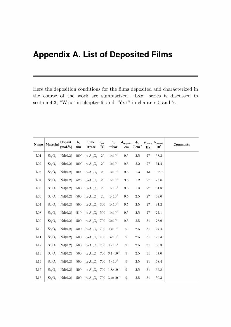
Appendix A. List of Deposited Films
Here the deposition conditions for the films deposited and characterized inthe course of the work are summarized. “Lxx” series is discussed insection 4.3; “Wxx” in chapter 6; and “Yxx” in chapters 5 and 7.
Name MaterialDopant(mol.%)
h,nm
Sub-strate
Tsub,°C
PO2,mbar
dtarg-sub,cm
Φ,J⋅cm-2
νlaser,Hz
Npulses,103 Comments
L01 Sc2O3 Nd(0.2) 1000 α-Al2O3 20 1×10⁻³ 9.5 2.5 27 38.3
L02 Sc2O3 Nd(0.2) 1000 α-Al2O3 20 1×10⁻³ 9.5 2.2 27 61.4
L03 Sc2O3 Nd(0.2) 1000 α-Al2O3 20 1×10⁻³ 9.5 1.3 43 158.7
L04 Sc2O3 Nd(0.2) 525 α-Al2O3 20 1×10⁻³ 9.5 1.2 27 76.8
L05 Sc2O3 Nd(0.2) 500 α-Al2O3 20 1×10⁻³ 9.5 1.8 27 51.8
L06 Sc2O3 Nd(0.2) 500 α-Al2O3 20 1×10⁻³ 9.5 2.5 27 39.0
L07 Sc2O3 Nd(0.2) 500 α-Al2O3 300 1×10⁻³ 9.5 2.5 27 31.2
L08 Sc2O3 Nd(0.2) 510 α-Al2O3 500 1×10⁻³ 9.5 2.5 27 27.1
L09 Sc2O3 Nd(0.2) 500 α-Al2O3 700 3×10⁻⁴ 9.5 2.5 31 28.9
L10 Sc2O3 Nd(0.2) 500 α-Al2O3 700 1×10⁻³ 9 2.5 31 27.4
L11 Sc2O3 Nd(0.2) 500 α-Al2O3 700 3×10⁻³ 9 2.5 31 26.4
L12 Sc2O3 Nd(0.2) 500 α-Al2O3 700 1×10⁻² 9 2.5 31 50.3
L13 Sc2O3 Nd(0.2) 500 α-Al2O3 700 3.1×10⁻² 9 2.5 31 47.0
L14 Sc2O3 Nd(0.2) 500 α-Al2O3 700 1×10⁻¹ 9 2.5 31 68.4
L15 Sc2O3 Nd(0.2) 500 α-Al2O3 700 1.8×10⁻² 9 2.5 31 36.8
L16 Sc2O3 Nd(0.2) 500 α-Al2O3 700 3.4×10⁻² 9 2.5 31 50.3
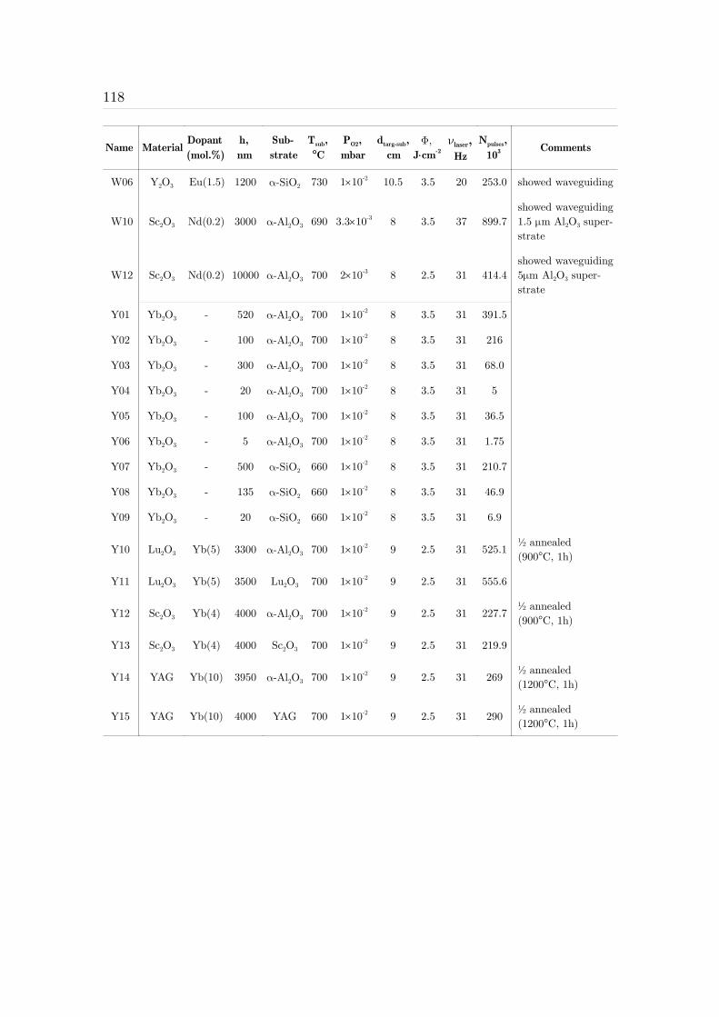
118
Name MaterialDopant(mol.%)
h,nm
Sub-strate
Tsub,°C
PO2,mbar
dtarg-sub,cm
Φ,J⋅cm-2
νlaser,Hz
Npulses,103 Comments
W06 Y2O3 Eu(1.5) 1200 α-SiO2 730 1×10⁻² 10.5 3.5 20 253.0 showed waveguiding
W10 Sc2O3 Nd(0.2) 3000 α-Al2O3 690 3.3×10⁻³ 8 3.5 37 899.7showed waveguiding1.5 μm Al2O3 super-strate
W12 Sc2O3 Nd(0.2) 10000 α-Al2O3 700 2×10⁻³ 8 2.5 31 414.4showed waveguiding5μm Al2O3 super-strate
Y01 Yb2O3 - 520 α-Al2O3 700 1×10⁻² 8 3.5 31 391.5
Y02 Yb2O3 - 100 α-Al2O3 700 1×10⁻² 8 3.5 31 216
Y03 Yb2O3 - 300 α-Al2O3 700 1×10⁻² 8 3.5 31 68.0
Y04 Yb2O3 - 20 α-Al2O3 700 1×10⁻² 8 3.5 31 5
Y05 Yb2O3 - 100 α-Al2O3 700 1×10⁻² 8 3.5 31 36.5
Y06 Yb2O3 - 5 α-Al2O3 700 1×10⁻² 8 3.5 31 1.75
Y07 Yb2O3 - 500 α-SiO2 660 1×10⁻² 8 3.5 31 210.7
Y08 Yb2O3 - 135 α-SiO2 660 1×10⁻² 8 3.5 31 46.9
Y09 Yb2O3 - 20 α-SiO2 660 1×10⁻² 8 3.5 31 6.9
Y10 Lu2O3 Yb(5) 3300 α-Al2O3 700 1×10⁻² 9 2.5 31 525.1½ annealed(900°C, 1h)
Y11 Lu2O3 Yb(5) 3500 Lu2O3 700 1×10⁻² 9 2.5 31 555.6
Y12 Sc2O3 Yb(4) 4000 α-Al2O3 700 1×10⁻² 9 2.5 31 227.7½ annealed(900°C, 1h)
Y13 Sc2O3 Yb(4) 4000 Sc2O3 700 1×10⁻² 9 2.5 31 219.9
Y14 YAG Yb(10) 3950 α-Al2O3 700 1×10⁻² 9 2.5 31 269½ annealed(1200°C, 1h)
Y15 YAG Yb(10) 4000 YAG 700 1×10⁻² 9 2.5 31 290½ annealed(1200°C, 1h)
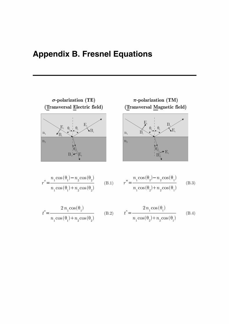
Appendix B. Fresnel Equations
σ-polarization (TE)(Transversal Electric field)
EiEr
Et
Bin1
n2
Br
Bt
θ1 θ1
θ2
rσ=n
1cos θ
1n
2cos θ
2
n1cos θ
1n
2cos θ
2
(B.1)
tσ=2n
1cosθ
1
n1cos θ
1n
2cos θ
2
(B.2)
π-polarization (TM)(Transversal Magnetic field)
Ei
Er
Et
Bin1
n2
Br
Bt
θ1 θ1
θ2
r=n
1cos θ
2n
2cosθ
1
n1cos θ
2n
2cosθ
1
(B.3)
tπ=2n
1cos θ
1
n1cosθ
2n
2cos θ
1
(B.4)
120
Bibliography
[Abr78] V. N. Abramov and A. I. Kuznetsnov, Fundamental absorption ofY2O3 and YAlO3, Sov. Phys. Solid State, 20 (3) (1978) 399.
[And97] A. A. Anderson, R.W. Eason, L. M. B. Hickey, M. Jelinek, C. Grivas, D. S. Gill, and N. A. Vainos, Ti:Sapphire planar waveguidelaser grown by pulsed laser deposition, Opt. Lett., 22 (1997) 1556-8.
[And97a] A. A. Anderson, R. W. Eason, M. Jelinek, C. Grivas, D. Lane, K. Rogers, L. M. B. Hickey, and C. Fotakis, Growth of Ti:sapphiresingle crystal thin films by pulsed laser deposition, Thin Solid Films,300 (1997) 68-71.
[And97b] A. A. Anderson, R. W. Eason, L. M. B. Hickey, M. Jelinek, C.Grivas, D. S. Gill, and N. A. Vainos, Ti:sapphire planar waveguidelaser grown by pulsed laser deposition, Opt. Lett., 22 (1997) 1556-8.
[And98] A. A. Anderson, Crystalline Planar Waveguide Lasers Fabricated byPulsed Laser Deposition. PhD Thesis, University of Southampton,1998.
[Ata00] P. A. Atanasov, R. I. Tomov, J. Perriere, R. W. Eason, N. Vainos, A. Klini, A. Zherikhin, and E. Millon, Growth of Nd: potassiumgadolinium tungstate thin-film waveguides by pulsed laser deposition,Appl. Phys. Lett., 76 (2000) 2490.
[Aul82] B. F. Aull and H. P. Jenssen, Vibronic Interactions in Nd:YAGResulting in Nonreciprocity of Absorption and Stimulated EmissionCross Sections, IEEE J. of Quant. Electr., 18 (1982) 925.
[Bar01] S. J. Barrington, Planar Waveguide Devices Fabricated by PulsedLaser Deposition. PhD Thesis, University of Southampton, 2001.
[Bär04] S. Bär, Crystalline Rare-Earth-doped Sesquioxide PLD-Films on α-Alumina (preparation and characterization). Dissertation, Institut für Laser-Physik, Universität Hamburg, 2004.
[Bär05] S. Bär, unpublished results (Institut für Laser-Physik, UniversitätHamburg, 2005).
121
[Bar57] C. Barta, F. Petru and B. Hajek, Über die Darstellung desEinkristalls von Scandiumoxyd, Die Naturwissenschaften, 45 (1957)36.
[Bäu00] D. Bäuerle, Laser Processing and Chemistry (Springer-Verlag, Berlin,Heidelberg, New York, 2000).
[Bjö96] G. Björk, Microcavity Lasers and QED (in Laser Sources andApplications: Proceedings of the Forty Seventh Scottish UniversitiesSummer School in Physics, St. Andrews /ed. by A. Miller and D. M.Finlayson), Institute of Physics, Bristol, 1996.
[Bon00] C. L. Bonner, Mult-Wat, Diode-Pumped Planar Waveguide Lasers.PhD Thesis, University of Southampton, 2000.
[Bos04] A. Bosco, M. Centini, L. Sciscione, C. Sibilia, E. Fazio, M. Bertolotti,A. Fiore, A. Convertino, L. Cerri, and M. Scalora, Nonlinear type-IIsecond-harmonic generation in AlGaAs/Al2O3 one-dimentionalphotonic crystal, Appl. Phys. Lett., 84 (2004) 16.
[Bru04] F. Brunner, E. Innerhofer, S. V. Marchese, T. Südmeyer, R. Paschotta, T. Usami, H. Ito, S. Kurimura, K. Kitamura, G. Arisholm, and U. Keller, Powerful red-green-blue laser sourcepumped with a mode-locked thin disk laser, Opt. Lett., 29 (2004) 1921-3.
[Bur02] P. Burmester, Optisch aktive, kristalline, Selten Erd-dotierte Y2O3-PLD-Schichten auf α-Al2O3. Dissertation, Institut für Laser-Physik, Universität Hamburg, 2002.
[Cha63] N. C. Chang, Fluorescence and Stimulated Emisson from TrivalentEuropium in YttriumOxide, J. Appl. Phys., 34 (1963) 3500.
[Cha72] D. J. Channin,J. M. Hammer, J. P. Wittke, Dispersion and loss innew thin-film optical waveguides, IEEE J. Quantum Elect., 8 (1972) 6.
[Cha92] I. Chartier, B. Ferrand, D. Pelenc, S. J. Field, D. C. Hanna, A. C. Large, D. P. Shepherdund A. C. Tropper, Growth and low-threshold laser oscillation of an epitaxially grown Nd:YAG waveguide,Opt. Lett., 17 (1992) 810.
122
[Chi99] W. Y. Ching and Y.-N. Xu, Nonscalability and nontransferability inthe electronic properties of the Y-Al-O system, Phys. Rev. B, 59 (1999) 12815-21.
[Chr94] D. B. Chrisey and G. K. Hubler, Pulsed Laser Deposition of ThinFilms (John Wiley & Sons, Inc., New York, 1994).
[Cru03] A. Crunteanu, G. Jänchen, P. Hoffmann, M. Pollnau, C. Buchal, A. Petraru, R. W. Eason, and D. P. Shepherd, Three-dimentionalstructuring of sapphire by sequential He+ ion-beam implantation andwet chemical etching, Appl. Phys. A, 76 (2003) 1109-12.
[Cul78] B. D. Cullity, Elements of X-ray Diffraction (Addison-Wesley,London, 1978).
[DeM88] F. De Martini and G. R. Jacobovitz, Anomalous sponteneous-stimulated-decay phase transition and zero-threshold laser action in a microscopic cavity, Phys. Rev. Lett., 60 (1988) 1711-4.
[Dex53] D. L. Dexter, A Theory of Sensitzed Luminescence in Solids, J. Chem. Phys., 21 (1953) 836-50.
[Dij87] D. Dijkamp, T. Venkatesan, X. D. Wu, S. A. Shaheen, N. Jisrawi, Y. H. Min-Lee, W. L. McLean, and M. Croft., Preparation of Y-Ba-Cu oxide superconductorthin films using pulsed laserevaporation from high Tc bulk material, Appl. Phys. Lett., 51 (1987)619.
[Dri04] A. Driessen, D. H. Geuzebroek, H. J. W. M. Hoekstra, H. Kelderman,E. J. Klein, D. J. W. Klunder, C. G. H. Roeloffzen, F. S. Tan, E.Krioukov, C. Otto, H. Gersen, N. F. van Hulst, and L. Kuipers,Microresonators as building blocks for VLSI Photonics (invitedLecture) (in AIP Conference Proceedings Vol. 709. Proceedings ofInternational School of Quantum Electronics, Erice-Sicily, 2003),2004, pp. 1-18.
[Ehl05] S. Ehlert, Herstellung und Charakterzsierung ultradünner PLD-Sesquioxidschichten auf Quartz. Diplomarbeit, Institut für Laser-Physik, Universität Hamburg, 2005.
123
[Eza96] M. Ezaki, M. Obara, H. Kumagai, and K. Toyoda, Characterizationof Nd:Y3Al5O12 thin films grown on varoius subsrates by pulsed laserdeposition, Appl. Phys. Lett., 69 (1996) 2977-9.
[Fin66] D. Findley and R. Clay, The measurements of internal losses in 4-level lasers, Phys. Lett., 20 (1966) 3.
[För48] T. Förster, Zwischenmolekulare Energiewanderung und Fluoreszenzen,Annalen der Physik, 2 (1948) 55-75.
[For99] L. Fornasiero, Nd3+ und Tm3+-dotierte Sesquioxide. Dissertation,Institut für Laser-Physik, Universität Hamburg, 1999.
[For99a] L. Fornasiero, E. Mix, V. Peters, E. Heumann, K. Petermann, and G. Huber, Efficient Laser Operation of Nd:Sc2O3 at 966 nm, 1082nm, and 1486 nm (in OSA Trends in Optics and Photonics. Vol.26.Advanced Solid-State Lasers. /ed. by M. M. Fejer, H. Inejeyan, andU. Keller), Opt. Soc. America, Washington, DC, USA, 1999.
[Fre90] R. H. French, Electronic Structure of α-Al2O3 , with Comparison toAlON and AlN, J. Am. Chem. Soc., 73 (1990) 477-89.
[Ger04] H. Gersen, D. J. W. Klunder, J. P. Korterik, A. Driessen, N. F. van Hulst, and L. Kuipers, Propagation of a femtosecond pulsein a microresonator visualized in time, Opt. Lett., 29 (2004) 1291-3.
[Gie94] A. Giesen, H. Hügel, A. Voss, K. Wittig, U. Brauch, and H. Opower,Scalable Concept for Diode-Pumped High-Power Solid-State Lasers,Appl. Phys. B, 58 (1994) 365-72.
[Gil96] D. S. Gill, A. A. Anderson, R. W. Eason, T. J. Warburton, and D. P. Shepherd, Laser operation of an Nd:Gd3Ga5O12 thin-film opticalwaveguide fabricated by pulsed laser deposition, Appl. Phys. Lett., 69(1996) 10-12.
[Gri04a] C. Grivas, T. C. May-Smith, D. P. Shepherd, R. W. Eason, Laseroperation of a low loss (0.1 dB/cm) Nd:Gd3Ga5O12 thick (40μm)planar waveguide grown by pulsed laser deposition, Opt. Commun.,229 (2004) 355-61.
124
[Gri04b] C. Grivas, T. C. May-Smith, D. P. Shepherd, R. W. Eason, On thegrowth and lasing characteristics of thick Nd:GGG waveguiding filmsfabricated by pulsed laser deposition, Appl. Phys. A, 79 (2004) 1203-06.
[Gri04c] C. Grivas, T. C. May-Smith, D. P. Shepherd, R. W. Eason, M. Pollnau, and M. Jelinek, Broadband single-transverse-modefluorescence sources based on ribs fabricated in pulsed laser depositedTi:sapphire waveguides, Appl. Phys. A, 79 (2004) 1195-98.
[Grib04] U. Griebner, V. Petrov, K. Petermann, and V. Peters, Passivelymode-locked Yb:Lu2O3 laser, Opt. Express, 12 (2004) 3125-30.
[Gup91] A. Gupta, B. W. Hussey, A. Kussmaul, and A. Segmuller, Defectformation caused by a transient decrease in the ambient oxygenconcentration during growth of YBa2Cu3O7-x films, Appl. Phys. Lett.,57 (1991) 2365-7.
[Hic98] L. M. B. Hickey, Ti:sapphire waveguide laser by thermal diffusion oftitanium into sapphire. PhD Thesis, University of Southampton,1998.
[Hoe66] H. R. Hoekstra, Phase relationships in the rare-earth sesquioxides,Inorg. Chem., 5 (1966) 754.
[Hos64] R. H. Hoskins and B. H. Soffer, Stimulated Emission from Y2O3:Nd3+,Appl. Phys. Lett., 4 (1964) 22.
[Ibr04] T. A. Ibrahim, K. Amarnath, L. C. Kuo, R. Grover, V. Van, and P.-T. Ho, Photonic logic NOR gate based on two symmetric microringresonators, Opt. Lett., 29 (2004) 1579-81.
[Kah05] A. Kahn, Verlustmessungen an Nd3+ dotierten planaren Wellenleiternand deren Charakterisierung für Laseranwendungen. Diplomarbeit,Universität Hamburg, 2005.
[Kik03] P. G. Kik and A. Polman, Cooperative upconversion as the gain-limiting factor in Er doped miniature Al2O3 optical waveguideamplifiers, J. Appl. Phys., 93 (2003) 5008-12.
125
[Kle05] D. O. Klenov, L. F. Edge, D. G. Schlom,and S. Stemmer, Extendeddefects in epitaxial Sc2O3 films grown on (111) Si, Appl. Phys. Lett.,86 (2005) 51901-3.
[Klo04] P. Klopp, V. Petrov, U. Griebner, K. Petermann, V. Peters, and G.Erbert, Highly efficient mode-locked Yb:Sc2O3 laser, Opt. Lett., 29 (2004) 391-3.
[Kor01] M. B. Korzenski, P. Lecoeur, B. Mercey, P. Camy, and J. L. Doualan,Low propagation losses of an Er:Y2O3 planar waveguide grown byalternate-target pulsed laser deposition, Appl. Phys. Lett., 78 (2001)1210.
[Kuz04] Y. Kuzminykh, S. Bär, H. Scheife, G. Huber, V. Apostolopoulos, andM. Pollnau, Waveguiding thin Y2O3 films grown on sapphiresubstrates (in Europhysics Conference Abstracts Volume 28C.Proceedings of the 1st EPS-QEOD Europhoton Conference), 2004,Fib10128 (ThC25).
[Kuz06] Y. Kuzminykh, A. Kahn, and G. Huber, Nd3+ doped Sc2O3
waveguiding film produced by pulsed laser deposition, Opt. Mater., 28 (2006) 883-7.
[Lan04] J. Lancok, C. Garapon, C. Martinet, J. Mugnier, and R. Brenier,Influence of the PLD parameters on the crystalline phases andflourescence of Eu:Y2O3 planar waveguides, Appl. Phys. A, 79 (2004)1263-65.
[Lan05] J. Lancok, C. Garapon, M. Jelinek, J. Mugnier, and R. Brenier,Optical and structural properties of Pr:GGG crystalline thin filmwaveguides grown by pulsed-laser deposition, Appl. Phys. A, 81 (2005)1477-83.
[Lar05] M. Larionov, K. Schuhmann, J. Speiser, C. Stolzenburg and A.Giesen, Nonlinear decay of the excited state in Yb:YAG (in AdvancedSolid-State Photonics 2005 Technical Digest on CD-ROM), 2005,TuB49.
[Lee86] D. H. Lee, Electromagnetic Principles of Integrated Optics (JohnWiley & Sons, New York, 1986).
126
[Lev62] R. A. Lefever, Flame Fusion Growth of C-Type Rare-Earth Oxides,Rev. Sci. Instr., 33 (1962) 1470.
[Mac01] J. I. Mackenzie, C. Li, D. P. Shepherd, H. E. Meissner, and S. C.Mitchell, Longitudinally diode-pumped Nd:YAG double-clad planarwaveguide laser, Opt. Lett., 26 (2001) 10.
[Mix99] E. Mix, Kristallzüchtung, Spektroskopie und Lasereingenschaften Yb-dotierter Sesquioxide. Dissertation, Institut für Laser-Physik,Universität Hamburg, 1999.
[Möl86] T. Möller, P. Gürtler, E. Roick, and G. Zimmerer, The experimentalstation SUPERLUMI: a unique setup for time- and spectrally resolvedluminescence under state selective excitation with synchrotronradiation, Nucl. Instrum. Meth. Phys. Res. A, 246 (1986) 461-4.
[NDL] NASA Database of Laser Materials.
[Neg03] E. Negodine, Inter- and intraconfigurational luminescence ofLiYF4:Er3+ under selective VUV excitation. Dissertation, UniversitätHamburg, 2003.
[Pay92] S. A. Payne, L. L. Chase, L. K. Smith, W. L. Kway, and W. F.Krupke, Infrared Cross-Section Measurements for Crystals Dopedwith Er3+,Tm3+ and Ho3+, IEEE J. of Quant. Electr., 28 (1992) 2619.
[Pet01] V. Peters, Growth and Spectroscopy of Ytterbium-Doped Sesquioxides.Dissertation, Institut für Laser-Physik, Universität Hamburg, 2001.
[Pet02a] V. Peters, A. Bolz, K. Petermann, and G. Huber, Growth of high-melting sesquioxides by the heat-exchanger method, J. Cryst. Growth, 237-9 (2002) 879-83.
[Pet02b] K. Petermann, L. Fornasiero, E. Mix and V. Peters, High meltingsesquioxides: crystal growth, spectroscopy, and laser experiments, Opt. Mater., 19 (2002) 67-71.
[Pet05] K. Petermann, D. Fagundes-Peters, J. Johannsen, M. Mond, V. Peters, J. J. Romero, S. Kutovoi, J. Speiser, A. Giesen, Highly Yb-doped oxides for thin-disk lasers, J. Cryst. Growth, 275 (2005) 135-40.
127
[Pie01] L. van Pieterson, Charge Transfer and 4f n ↔ 4f n-15d Luminescence ofLanthanide Ions. Proefschrift, Universiteit Utrecht, 2001.
[Pur46] E. M. Purcell, Spontaneous Emission Probabilities at RadioFrequencies, Phys. Rev., 69 (1946) 681.
[Rab04] L. Rabisch, Ultradünne, Eu-dotierte, thermisch aufgedampfteSesquioxid-Schichten auf α-Al2O3-Substraten. Dissertation, Institut für Laser-Physik, Universität Hamburg, 2004.
[Rot60] R. S. Roth and S. J. Schneider, Phase equilibria in the systemsinvolving the rare-earth oxides, J. Res. Nat. Bur. Stand., 64A (1960) 309.
[Sae93a] K. L. Sanger, Pulsed laser deposition: Part I – A review of processcharacteristics and capabilities, Proc. of Adv. Mat., 2 (1993) 1-24.
[Sae93b] K. L. Sanger, Pulsed laser deposition: Part II – A review of processmechanisms, Proc. of Adv. Mat., 3 (1993) 63-82.
[Sco90] K. Scott, J. M. Huntley, W. A. Phillips, J. Clarke, and J. E. Field,Influence of oxygen pressure on laser ablation of YBa2Cu3O7-x, Appl.Phys. Lett., 57 (1990) 922-4.
[Smi65] H. M. Smith and A. F. Turner, Vacuum deposited thin films using aruby laser, Appl. Optics, 4 (1965) 147-8.
[Son98] J. Sonsky, J. Lancok, M. Jelinek, J. Oswald, and V. Studniska,Growth of active Nd-doped YAP thin-film waveguides by laserablation, Appl. Phys. A, 66 (1998) 583-6.
[Ste00] C. Stewen, M. Larionov, A. Giesen, K. Contag, Yb:YAG thin disklaser with 1kW output power (in OSA Trends in Optics andPhotonics. Vol. 34. Advanced Solid-State Lasers. /ed. by H. Inejeyan,U. Keller, C. Marschall), Opt. Soc. America, Washington, DC, USA,2000.
[Tom86] T. Tomiki, J. Tamashiro, Y. Tanahara, A. Yamada, H. Fukutani, T. Miyahara, H. Kato, S. Shin, and M. Ishigame, Optical Spectra ofY2O3 Single Crystals in VUV, J. Phys. Soc. Jpn., 55 (1986) 4543.
128
[Tro04] A. C. Tropper, H. D. Foreman, A. Garnache. K.G: Wilcox, and S. H. Hoogland, Vertical-external-cavity semiconductor lasers, J Phys. D: Appl. Phys., 37 (2004) R75-R85.
[Ubi04] S. B. Ubizskii, A. O. Matkovskii, S. S. Melnyk, I. M. Syvorotka, V. Müller, V. Peters, K. Petermann, A. Beyertt, and A. Giesen,Optical properties of epitaxial YAG:Yb films, phys. stat. sol. (a), 201 (2004) 791-7.
[Via00] B. Viana, O. Pons-y-Mall, N. Degory, E. Antic-Fidaneev, E. Millun,J. Perriere, C. Beloue, Optical properties of rare earth doped yttriumoxide waveguides (in Conference Digest. 2000 Conference on Lasersand Electro-Optics Europe), 2000, p.384.
[Vog05] A. Vogel, J. Noack, G. Hüttman, and G. Paltauf, Mechanisms offemtosecond laser nanosurgery of cells and tissues, Appl. Phys. B, 81 (2005) 1015-47.
[Xu91] Y.-N. Xu and W. Y. Ching, Self-consistent band structures, chargedistributions, and optical-absorption spectra in MgO, α-Al2O3, andMgAl2O4, Phys. Rev. B, 43 (1991) 4461.
[Xu97] Y.-N. Xu, Z.-q. Gu, and W. Y. Ching, Electronic, structural, andoptical properties of crystalline yttria, Phys. Rev. B, 56 (1997) 14993-15000.
[Xu99] Y.-N. Xu and W. Y. Ching, Electronic structure of yttrium aluminumgarnet (Y3Al5O12), Phys. Rev. B, 59 (1999) 10530-35.
[Yar89] A. Yariv, Quantum Electronics (John Wiley & Sons, New York,1989).
[Zel98] D. E. Zelmon, D. L. Small, and R. Page, Refractive-indexmeasurements of undoped yttrium aluminum garnet from 0.4 to 5.0 μm, Appl. Optics, 37 (1998) 4933-5.
[Zve67] G. M. Zverev, G. Ya. Kolodnyi, I. Smirnov, Optical Spectra of Nd3+
Single Crystals of Scandium and Yttrium Oxides, Opt. Spectrosc.(USSR), 32 (1967) 325-7.
129
Acknowledgments
This thesis results from more than three years of research at the Institute ofLaser Physics in Hamburg. It would not be possible without the help, assistanceand support of many people.
First of all I would like to thank my supervisor Prof. Dr. Günter Huber for theopportunity of the interesting PhD studies in the “Solid State Lasers” groupand support in accomplishing of this thesis. Also a lot of thanks to all membersof the group for the wonderful spirit both at work and at leisure time. Specialthanks goes to Dr. Sebastian Bär, Dr. Hanno Scheife, and Dr. Klaus Petermannfor proofreading of this thesis and for the numerous discussions, advices, andexplanations – whether related to the physics or concerning the “deutscheSprache, Behörden, Gesetze, ...”.
Many greetings to all my former and current 'neighbours', who shared the officewith me – Dr. Bert Neubert, Dr. Eugen Osiac, Dr. Takugo Ishii, BjörnMichaelsen, and René Hartke. I enjoyed your company.
A lot of experiments have been made together with my colleagues. So, a bigthanks to Friedjof Tellkamp, who helped to recondition the PLD-machine after“it happened again”, Stefan Ehlert, together with whom the first everPLD-films were grown, Andreas Kahn, who 'guided' the waveguide experiments,Dr. Katja Rademaker, who suggested to make stripes, not films, Dr. VolkerPeters, who teached me the 'real' crystal growth, Dr. Lutz Rabisch, for beingready to help anytime, and Bilge Ileri, for the 'last minute' measurements.
The technical assistance of Silke Frömmig, Robert Fischer, and Stephan Garbershelped to make many things faster and easier.
In the course of this work a number of collaborations arose. They excited manynew ideas and allowed to realize the experiments, which would not be possibleotherwise. So, many thanks to ...
... Dr. Gregory Stryganyuk and Prof. Dr. Georg Zimmerer at SuperLumi fora lot of opportunities to use the station, for assistance in the measurementsand helpful discussions.
130
... Michael Pfeifers, Christian Krug, and Prof. Dr. Christoph Platte atFachhochschule Wedel for the multiple possibilities to use their X-raydiffractometer.
... Dr. Vasilis Apostolopoulos and Dr. Marcus Pollnau at the EPF deLausanne for the introduction into the field of waveguides.
... Klaudia Hagemann, Manfred Spiwek, and Horst Schulte-Schrepping atHasyLab for providing the X-ray machine for crystal orientation.
... Thomas Lipinsky at the Forschungszentrum Jülich for the Ar+-beametching experiments.
... Jan Podbielski at the Institut für Angewandte Physik for the fabricationof the photoresist mask for the lift-off experiments.
Last but not least, I would like to thank my friends, family, and especially Lena,who supported me outside of the work and helped to make all this possible.
This work was financially supported through the Graduiertenkollegno. 463 “Spektroskopie an lokalisierten atomaren Systemen” funded by theDeutsche Forschungsgemeinschaft.