Embed Size (px)
Citation preview
File: ASPDAC2001_Sakai_差し替え版.docName: Satoshi SAKAIDANI
Time Date: 00/09/08 23:27Number of Words: 1119
Page:
Flexible Processor Based on Full-Adder / D-Flip-Flop Merged Module
Satoshi SAKAIDANI, Naoto MIYAMOTO, and Tadahiro OHMI1
Department of Electronic Engineering, Graduate School of Engineering, Tohoku University,05 Aza-Aoba, Aramaki, Aoba-ku, Sendai 980-8579, Japan
Phone/Fax: +81-22-217-7124/+81-22-263-9395, e-mail: [email protected] New Industry Creation Hatchery Center, Tohoku University, Aza-Aoba, Aramaki, Aoba-ku, Sendai 980-8579, Japan
Abstract– Flexible processor based on full-adder / D-flip-flopmerged module (FDMM) has been designed and fabricated. Thedeveloped FDMM has unique ability to perform both logic and flip-flop functions with a small transistor counts by merging commonpart of both circuit. We have also developed a context memory blockto reconfigure the hardware dynamically. The flexible processor mayfill a gap between hardware performance and software programma-bility to jump into a novel computing such as software / hardwaresynthesis; “software accelerator”.
I. INTRODUCTION
Flexible hardware architecture for a specific task on demand isone of the most important issues to bring out a novel-computingparadigm in the era of system LSI. This is because it can fill awide gap between hardware performance and software program-mability [1]. The gap has been shown, for instance, as a differencebetween application-specific LSI (ASIC) with intensive perfor-mance and field programmable gate array (FPGA) with intensiveprogrammability. Moreover, in conventional FPGA, customizablemodules are composed of large combinational logic part and op-tional flip-flop part to perform any functions by utilizing its vastprogrammability. Therefore, developing an original type of cus-tomizable module that has both ASIC’s and FPGA’s merit, whicheliminates redundant programmability preserving necessary speci-fic functionalities for performance, is most promising in order torealize a flexible processor. This is our focus.
We have developed an original flexible module, full-adder /D-flip-flop merged module (FDMM), and fabricated a chip in-cluding 4 x 4 array of FDMMs with 0.6µm CMOS technology.Utilizing our circuitry concept, we are aiming to apply this tosome signal processing schemes used in some multi-media appli-cations, and finally to realize a “software accelerator” for a soft-ware / hardware synthesis.
In this paper, we propose the developed FDMM and introducethe fabricated chip design and system architecture of flexibleprocessor based on FDMM in detail.
II. FULL-ADDER / D-FLIP-FLOP MERGED MODULE (FDMM)A schematic and operation of FDMM are shown in Fig. 1.
This module is composed of main functional block (shaded) andsub-control part. This module can be operated in multi-mode.When a control signal “sel” = 1, the module acts as a full-addercircuit (Logic MODE); and when “sel” = 0, it acts as a D-flip-flopcircuit (Flip-flop MODE). Note that FDMM has an ability toperform both logic and flip-flop functions with a small transistorcounts by merging common part of full-adder and D-flip-flopcircuit in contrast with traditional logic modules in FPGAs, these
are preparing both logic and flip-flop inside. It is a characteristicfeature of this study.
From the viewpoint of logic functionality, full-adder can real-ize sufficient logic functions such as 3-XOR, 3-Majority, 2-AND,2-OR, 2-XOR, 2-XNOR, etc. It is suitable essentially for arith-metic operation based on AND/OR signal processing that is fre-quently used in multi-media applications besides.
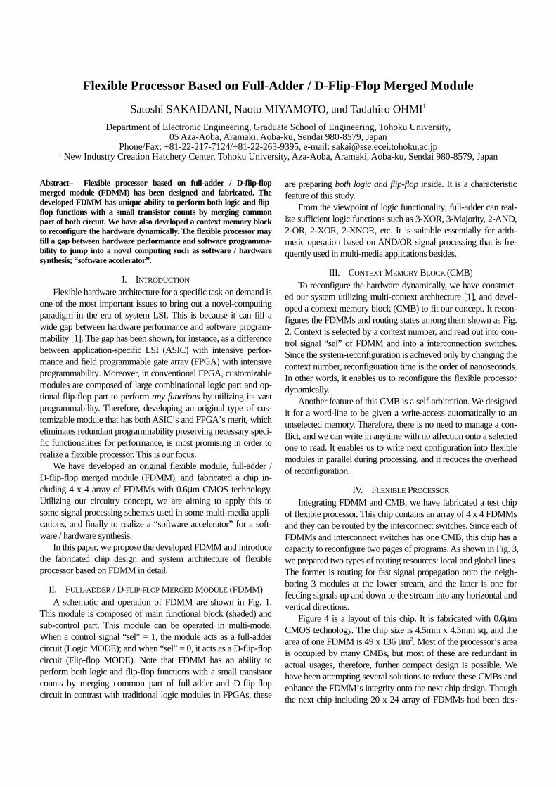
III. CONTEXT MEMORY BLOCK (CMB)To reconfigure the hardware dynamically, we have construct-
ed our system utilizing multi-context architecture [1], and devel-oped a context memory block (CMB) to fit our concept. It recon-figures the FDMMs and routing states among them shown as Fig.2. Context is selected by a context number, and read out into con-trol signal “sel” of FDMM and into a interconnection switches.Since the system-reconfiguration is achieved only by changing thecontext number, reconfiguration time is the order of nanoseconds.In other words, it enables us to reconfigure the flexible processordynamically.
Another feature of this CMB is a self-arbitration. We designedit for a word-line to be given a write-access automatically to anunselected memory. Therefore, there is no need to manage a con-flict, and we can write in anytime with no affection onto a selectedone to read. It enables us to write next configuration into flexiblemodules in parallel during processing, and it reduces the overheadof reconfiguration.
IV. FLEXIBLE PROCESSOR
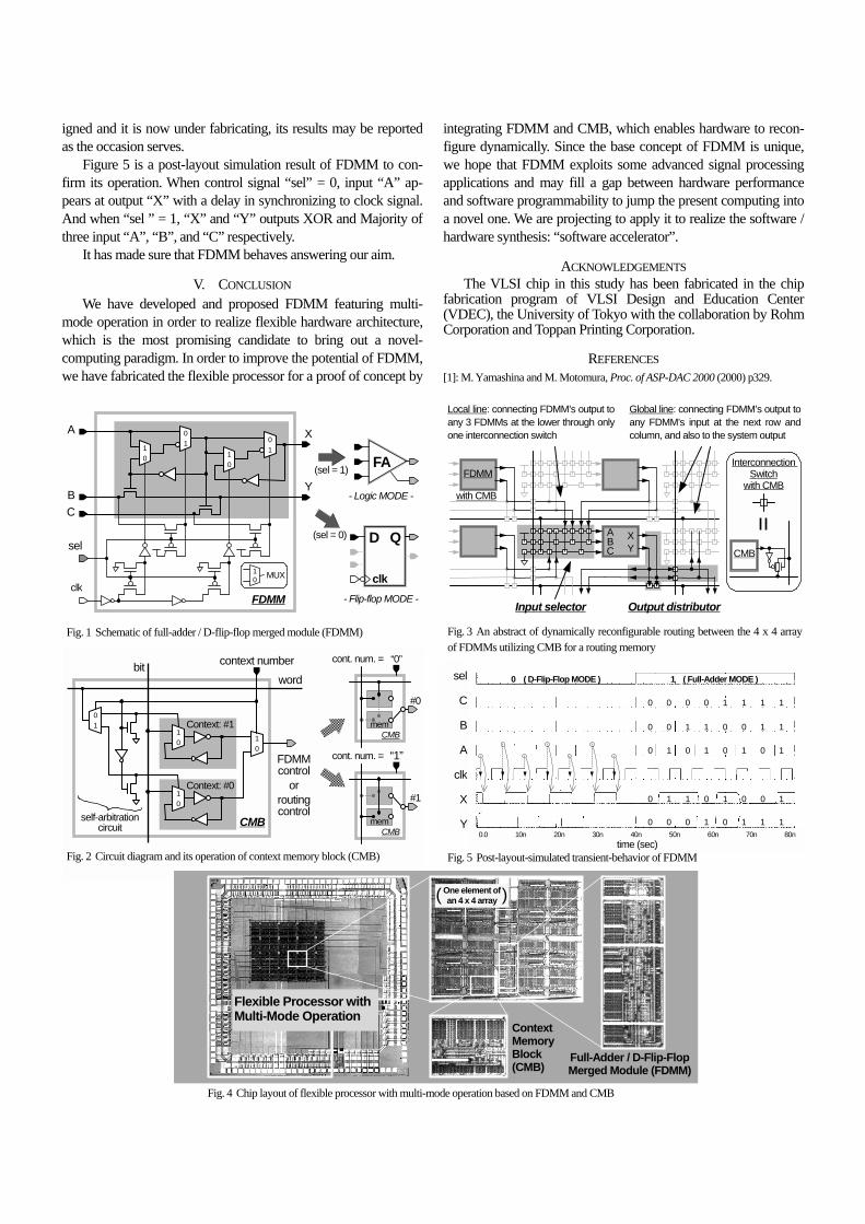
Integrating FDMM and CMB, we have fabricated a test chipof flexible processor. This chip contains an array of 4 x 4 FDMMsand they can be routed by the interconnect switches. Since each ofFDMMs and interconnect switches has one CMB, this chip has acapacity to reconfigure two pages of programs. As shown in Fig. 3,we prepared two types of routing resources: local and global lines.The former is routing for fast signal propagation onto the neigh-boring 3 modules at the lower stream, and the latter is one forfeeding signals up and down to the stream into any horizontal andvertical directions.
Figure 4 is a layout of this chip. It is fabricated with 0.6µmCMOS technology. The chip size is 4.5mm x 4.5mm sq, and thearea of one FDMM is 49 x 136 µm2. Most of the processor’s areais occupied by many CMBs, but most of these are redundant inactual usages, therefore, further compact design is possible. Wehave been attempting several solutions to reduce these CMBs andenhance the FDMM’s integrity onto the next chip design. Thoughthe next chip including 20 x 24 array of FDMMs had been des-
File: ASPDAC2001_Sakai_差し替え版.docName: Satoshi SAKAIDANI
Time Date: 00/09/08 23:27Number of Words: 1119
Page:
igned and it is now under fabricating, its results may be reportedas the occasion serves.
Figure 5 is a post-layout simulation result of FDMM to con-firm its operation. When control signal “sel” = 0, input “A” ap-pears at output “X” with a delay in synchronizing to clock signal.And when “sel ” = 1, “X” and “Y” outputs XOR and Majority ofthree input “A”, “B”, and “C” respectively.
It has made sure that FDMM behaves answering our aim.
V. CONCLUSION
We have developed and proposed FDMM featuring multi-mode operation in order to realize flexible hardware architecture,which is the most promising candidate to bring out a novel-computing paradigm. In order to improve the potential of FDMM,we have fabricated the flexible processor for a proof of concept by
integrating FDMM and CMB, which enables hardware to recon-figure dynamically. Since the base concept of FDMM is unique,we hope that FDMM exploits some advanced signal processingapplications and may fill a gap between hardware performanceand software programmability to jump the present computing intoa novel one. We are projecting to apply it to realize the software /hardware synthesis: “software accelerator”.
ACKNOWLEDGEMENTSThe VLSI chip in this study has been fabricated in the chip
fabrication program of VLSI Design and Education Center(VDEC), the University of Tokyo with the collaboration by RohmCorporation and Toppan Printing Corporation.
REFERENCES[1]: M. Yamashina and M. Motomura, Proc. of ASP-DAC 2000 (2000) p329.
Fig. 2 Circuit diagram and its operation of context memory block (CMB)
CMB
10 1
0
01
context number
10
Context: #1
Context: #0
bitword
#0
“0”
#1
“1”
mem
mem
CMB
CMBself-arbitration
circuit
FDMMcontrol
orroutingcontrol
cont. num. =
cont. num. =
Fig. 1 Schematic of full-adder / D-flip-flop merged module (FDMM)
(sel = 1)
FDMMclk
10
A
BC
sel
X
Y
10 MUX
01
10
01
FA
(sel = 0) D Q
clk
- Logic MODE -
- Flip-flop MODE -
Fig. 4 Chip layout of flexible processor with multi-mode operation based on FDMM and CMB
Fig. 3 An abstract of dynamically reconfigurable routing between the 4 x 4 arrayof FDMMs utilizing CMB for a routing memory
ABC
XY
with CMB
Input selector Output distributor
Global line: connecting FDMM’s output toany FDMM’s input at the next row andcolumn, and also to the system output
Local line: connecting FDMM’s output toany 3 FDMMs at the lower through onlyone interconnection switch
FDMM
CMB
InterconnectionSwitch
with CMB
sel
C
B
A
clk
X
Y0.0 10n 20n 30n 40n 50n 60n 70n 80n
time (sec)
0 ( D-Flip-Flop MODE ) 1 ( Full-Adder MODE )
0 1 1 0 1 0 0 1
0 0 0 1 0 1 1 1
0 1 0 1 0 1 0 1
0 0 1 1 0 0 1 1
0 0 0 0 1 1 1 1
Fig. 5 Post-layout-simulated transient-behavior of FDMM
One element ofan 4 x 4 array( )
Flexible Processor withMulti-Mode Operation
Full-Adder / D-Flip-FlopMerged Module (FDMM)
ContextMemoryBlock(CMB)